JP5868437B2 - Method for producing silicon wafer for solar cell - Google Patents
Method for producing silicon wafer for solar cell Download PDFInfo
- Publication number
- JP5868437B2 JP5868437B2 JP2014009159A JP2014009159A JP5868437B2 JP 5868437 B2 JP5868437 B2 JP 5868437B2 JP 2014009159 A JP2014009159 A JP 2014009159A JP 2014009159 A JP2014009159 A JP 2014009159A JP 5868437 B2 JP5868437 B2 JP 5868437B2
- Authority
- JP
- Japan
- Prior art keywords
- weight
- silicon wafer
- acid
- etching
- hydrofluoric acid
- Prior art date
- Legal status (The legal status is an assumption and is not a legal conclusion. Google has not performed a legal analysis and makes no representation as to the accuracy of the status listed.)
- Expired - Fee Related
Links
- 229910052710 silicon Inorganic materials 0.000 title claims description 115
- 239000010703 silicon Substances 0.000 title claims description 115
- XUIMIQQOPSSXEZ-UHFFFAOYSA-N Silicon Chemical compound [Si] XUIMIQQOPSSXEZ-UHFFFAOYSA-N 0.000 title claims description 114
- 238000004519 manufacturing process Methods 0.000 title claims description 16
- KRHYYFGTRYWZRS-UHFFFAOYSA-N Fluorane Chemical compound F KRHYYFGTRYWZRS-UHFFFAOYSA-N 0.000 claims description 107
- 238000005530 etching Methods 0.000 claims description 98
- QAOWNCQODCNURD-UHFFFAOYSA-N Sulfuric acid Chemical compound OS(O)(=O)=O QAOWNCQODCNURD-UHFFFAOYSA-N 0.000 claims description 78
- GRYLNZFGIOXLOG-UHFFFAOYSA-N Nitric acid Chemical compound O[N+]([O-])=O GRYLNZFGIOXLOG-UHFFFAOYSA-N 0.000 claims description 44
- 229910017604 nitric acid Inorganic materials 0.000 claims description 44
- 239000006061 abrasive grain Substances 0.000 claims description 33
- 239000000203 mixture Substances 0.000 claims description 32
- 229910021420 polycrystalline silicon Inorganic materials 0.000 claims description 23
- 239000002253 acid Substances 0.000 claims description 22
- XLYOFNOQVPJJNP-UHFFFAOYSA-N water Substances O XLYOFNOQVPJJNP-UHFFFAOYSA-N 0.000 claims description 16
- 229920005989 resin Polymers 0.000 claims description 9
- 239000011347 resin Substances 0.000 claims description 9
- 239000000126 substance Substances 0.000 claims description 9
- 238000010586 diagram Methods 0.000 claims description 7
- 235000012431 wafers Nutrition 0.000 description 112
- 239000000243 solution Substances 0.000 description 51
- 238000000034 method Methods 0.000 description 39
- 239000007864 aqueous solution Substances 0.000 description 28
- 239000010410 layer Substances 0.000 description 22
- 239000013078 crystal Substances 0.000 description 15
- QPJSUIGXIBEQAC-UHFFFAOYSA-N n-(2,4-dichloro-5-propan-2-yloxyphenyl)acetamide Chemical compound CC(C)OC1=CC(NC(C)=O)=C(Cl)C=C1Cl QPJSUIGXIBEQAC-UHFFFAOYSA-N 0.000 description 15
- 239000011162 core material Substances 0.000 description 12
- 239000007788 liquid Substances 0.000 description 9
- 238000006243 chemical reaction Methods 0.000 description 8
- 229910000831 Steel Inorganic materials 0.000 description 7
- 230000000052 comparative effect Effects 0.000 description 7
- 229910003460 diamond Inorganic materials 0.000 description 7
- 239000010432 diamond Substances 0.000 description 7
- 239000010959 steel Substances 0.000 description 7
- 239000002245 particle Substances 0.000 description 6
- 229910052751 metal Inorganic materials 0.000 description 5
- 239000002184 metal Substances 0.000 description 5
- 238000002156 mixing Methods 0.000 description 5
- 238000002310 reflectometry Methods 0.000 description 5
- PXHVJJICTQNCMI-UHFFFAOYSA-N Nickel Chemical compound [Ni] PXHVJJICTQNCMI-UHFFFAOYSA-N 0.000 description 4
- 238000005219 brazing Methods 0.000 description 4
- 230000001771 impaired effect Effects 0.000 description 4
- 230000001788 irregular Effects 0.000 description 4
- 239000000463 material Substances 0.000 description 4
- 238000007747 plating Methods 0.000 description 4
- 239000000843 powder Substances 0.000 description 4
- 229910000851 Alloy steel Inorganic materials 0.000 description 3
- 150000007513 acids Chemical class 0.000 description 3
- -1 aliphatic sulfonic acids Chemical class 0.000 description 3
- 150000001768 cations Chemical class 0.000 description 3
- 238000005520 cutting process Methods 0.000 description 3
- 238000003384 imaging method Methods 0.000 description 3
- VLTRZXGMWDSKGL-UHFFFAOYSA-N perchloric acid Chemical compound OCl(=O)(=O)=O VLTRZXGMWDSKGL-UHFFFAOYSA-N 0.000 description 3
- 101000982538 Homo sapiens Inositol polyphosphate 5-phosphatase OCRL Proteins 0.000 description 2
- 102100026724 Inositol polyphosphate 5-phosphatase OCRL Human genes 0.000 description 2
- NBIIXXVUZAFLBC-UHFFFAOYSA-N Phosphoric acid Chemical compound OP(O)(O)=O NBIIXXVUZAFLBC-UHFFFAOYSA-N 0.000 description 2
- 229910004298 SiO 2 Inorganic materials 0.000 description 2
- VYPSYNLAJGMNEJ-UHFFFAOYSA-N Silicium dioxide Chemical compound O=[Si]=O VYPSYNLAJGMNEJ-UHFFFAOYSA-N 0.000 description 2
- 229910000639 Spring steel Inorganic materials 0.000 description 2
- 239000000853 adhesive Substances 0.000 description 2
- 230000001070 adhesive effect Effects 0.000 description 2
- 230000007423 decrease Effects 0.000 description 2
- 238000004070 electrodeposition Methods 0.000 description 2
- 238000007373 indentation Methods 0.000 description 2
- 238000001000 micrograph Methods 0.000 description 2
- 229910021421 monocrystalline silicon Inorganic materials 0.000 description 2
- 229910052759 nickel Inorganic materials 0.000 description 2
- 235000011007 phosphoric acid Nutrition 0.000 description 2
- NROKBHXJSPEDAR-UHFFFAOYSA-M potassium fluoride Chemical compound [F-].[K+] NROKBHXJSPEDAR-UHFFFAOYSA-M 0.000 description 2
- FGIUAXJPYTZDNR-UHFFFAOYSA-N potassium nitrate Chemical compound [K+].[O-][N+]([O-])=O FGIUAXJPYTZDNR-UHFFFAOYSA-N 0.000 description 2
- 238000003825 pressing Methods 0.000 description 2
- HBMJWWWQQXIZIP-UHFFFAOYSA-N silicon carbide Chemical compound [Si+]#[C-] HBMJWWWQQXIZIP-UHFFFAOYSA-N 0.000 description 2
- 229910010271 silicon carbide Inorganic materials 0.000 description 2
- PUZPDOWCWNUUKD-UHFFFAOYSA-M sodium fluoride Chemical compound [F-].[Na+] PUZPDOWCWNUUKD-UHFFFAOYSA-M 0.000 description 2
- VWDWKYIASSYTQR-UHFFFAOYSA-N sodium nitrate Chemical compound [Na+].[O-][N+]([O-])=O VWDWKYIASSYTQR-UHFFFAOYSA-N 0.000 description 2
- LPXPTNMVRIOKMN-UHFFFAOYSA-M sodium nitrite Chemical compound [Na+].[O-]N=O LPXPTNMVRIOKMN-UHFFFAOYSA-M 0.000 description 2
- PCTMTFRHKVHKIS-BMFZQQSSSA-N (1s,3r,4e,6e,8e,10e,12e,14e,16e,18s,19r,20r,21s,25r,27r,30r,31r,33s,35r,37s,38r)-3-[(2r,3s,4s,5s,6r)-4-amino-3,5-dihydroxy-6-methyloxan-2-yl]oxy-19,25,27,30,31,33,35,37-octahydroxy-18,20,21-trimethyl-23-oxo-22,39-dioxabicyclo[33.3.1]nonatriaconta-4,6,8,10 Chemical compound C1C=C2C[C@@H](OS(O)(=O)=O)CC[C@]2(C)[C@@H]2[C@@H]1[C@@H]1CC[C@H]([C@H](C)CCCC(C)C)[C@@]1(C)CC2.O[C@H]1[C@@H](N)[C@H](O)[C@@H](C)O[C@H]1O[C@H]1/C=C/C=C/C=C/C=C/C=C/C=C/C=C/[C@H](C)[C@@H](O)[C@@H](C)[C@H](C)OC(=O)C[C@H](O)C[C@H](O)CC[C@@H](O)[C@H](O)C[C@H](O)C[C@](O)(C[C@H](O)[C@H]2C(O)=O)O[C@H]2C1 PCTMTFRHKVHKIS-BMFZQQSSSA-N 0.000 description 1
- PAWQVTBBRAZDMG-UHFFFAOYSA-N 2-(3-bromo-2-fluorophenyl)acetic acid Chemical compound OC(=O)CC1=CC=CC(Br)=C1F PAWQVTBBRAZDMG-UHFFFAOYSA-N 0.000 description 1
- KXGFMDJXCMQABM-UHFFFAOYSA-N 2-methoxy-6-methylphenol Chemical compound [CH]OC1=CC=CC([CH])=C1O KXGFMDJXCMQABM-UHFFFAOYSA-N 0.000 description 1
- DDFHBQSCUXNBSA-UHFFFAOYSA-N 5-(5-carboxythiophen-2-yl)thiophene-2-carboxylic acid Chemical compound S1C(C(=O)O)=CC=C1C1=CC=C(C(O)=O)S1 DDFHBQSCUXNBSA-UHFFFAOYSA-N 0.000 description 1
- RSWGJHLUYNHPMX-UHFFFAOYSA-N Abietic-Saeure Natural products C12CCC(C(C)C)=CC2=CCC2C1(C)CCCC2(C)C(O)=O RSWGJHLUYNHPMX-UHFFFAOYSA-N 0.000 description 1
- 229910000967 As alloy Inorganic materials 0.000 description 1
- 229910001369 Brass Inorganic materials 0.000 description 1
- OKTJSMMVPCPJKN-UHFFFAOYSA-N Carbon Chemical compound [C] OKTJSMMVPCPJKN-UHFFFAOYSA-N 0.000 description 1
- 229910000677 High-carbon steel Inorganic materials 0.000 description 1
- 229910001240 Maraging steel Inorganic materials 0.000 description 1
- KHPCPRHQVVSZAH-HUOMCSJISA-N Rosin Natural products O(C/C=C/c1ccccc1)[C@H]1[C@H](O)[C@@H](O)[C@@H](O)[C@@H](CO)O1 KHPCPRHQVVSZAH-HUOMCSJISA-N 0.000 description 1
- AZFNGPAYDKGCRB-XCPIVNJJSA-M [(1s,2s)-2-amino-1,2-diphenylethyl]-(4-methylphenyl)sulfonylazanide;chlororuthenium(1+);1-methyl-4-propan-2-ylbenzene Chemical compound [Ru+]Cl.CC(C)C1=CC=C(C)C=C1.C1=CC(C)=CC=C1S(=O)(=O)[N-][C@@H](C=1C=CC=CC=1)[C@@H](N)C1=CC=CC=C1 AZFNGPAYDKGCRB-XCPIVNJJSA-M 0.000 description 1
- 230000002378 acidificating effect Effects 0.000 description 1
- 239000004840 adhesive resin Substances 0.000 description 1
- 229920006223 adhesive resin Polymers 0.000 description 1
- 150000007933 aliphatic carboxylic acids Chemical class 0.000 description 1
- 229910045601 alloy Inorganic materials 0.000 description 1
- 239000000956 alloy Substances 0.000 description 1
- WUOACPNHFRMFPN-UHFFFAOYSA-N alpha-terpineol Chemical compound CC1=CCC(C(C)(C)O)CC1 WUOACPNHFRMFPN-UHFFFAOYSA-N 0.000 description 1
- 229910052782 aluminium Inorganic materials 0.000 description 1
- XAGFODPZIPBFFR-UHFFFAOYSA-N aluminium Chemical compound [Al] XAGFODPZIPBFFR-UHFFFAOYSA-N 0.000 description 1
- PNEYBMLMFCGWSK-UHFFFAOYSA-N aluminium oxide Inorganic materials [O-2].[O-2].[O-2].[Al+3].[Al+3] PNEYBMLMFCGWSK-UHFFFAOYSA-N 0.000 description 1
- 229910000147 aluminium phosphate Inorganic materials 0.000 description 1
- 150000001412 amines Chemical class 0.000 description 1
- CAMXVZOXBADHNJ-UHFFFAOYSA-N ammonium nitrite Chemical compound [NH4+].[O-]N=O CAMXVZOXBADHNJ-UHFFFAOYSA-N 0.000 description 1
- 238000005280 amorphization Methods 0.000 description 1
- 150000001450 anions Chemical class 0.000 description 1
- 239000010951 brass Substances 0.000 description 1
- 229910052799 carbon Inorganic materials 0.000 description 1
- 238000003486 chemical etching Methods 0.000 description 1
- 239000010960 cold rolled steel Substances 0.000 description 1
- 229910052802 copper Inorganic materials 0.000 description 1
- 230000006378 damage Effects 0.000 description 1
- 230000007547 defect Effects 0.000 description 1
- SQIFACVGCPWBQZ-UHFFFAOYSA-N delta-terpineol Natural products CC(C)(O)C1CCC(=C)CC1 SQIFACVGCPWBQZ-UHFFFAOYSA-N 0.000 description 1
- 230000000694 effects Effects 0.000 description 1
- 230000007613 environmental effect Effects 0.000 description 1
- 230000003628 erosive effect Effects 0.000 description 1
- 239000000945 filler Substances 0.000 description 1
- 150000004673 fluoride salts Chemical class 0.000 description 1
- 230000004907 flux Effects 0.000 description 1
- 238000000227 grinding Methods 0.000 description 1
- 238000007654 immersion Methods 0.000 description 1
- 239000012535 impurity Substances 0.000 description 1
- 230000001678 irradiating effect Effects 0.000 description 1
- 230000031700 light absorption Effects 0.000 description 1
- 238000005259 measurement Methods 0.000 description 1
- 238000002844 melting Methods 0.000 description 1
- 230000008018 melting Effects 0.000 description 1
- 239000011259 mixed solution Substances 0.000 description 1
- 150000002823 nitrates Chemical class 0.000 description 1
- 150000002826 nitrites Chemical class 0.000 description 1
- 239000003921 oil Substances 0.000 description 1
- 150000007524 organic acids Chemical class 0.000 description 1
- 235000005985 organic acids Nutrition 0.000 description 1
- 239000007800 oxidant agent Substances 0.000 description 1
- 238000007254 oxidation reaction Methods 0.000 description 1
- VLTRZXGMWDSKGL-UHFFFAOYSA-M perchlorate Inorganic materials [O-]Cl(=O)(=O)=O VLTRZXGMWDSKGL-UHFFFAOYSA-M 0.000 description 1
- 230000002093 peripheral effect Effects 0.000 description 1
- 239000005011 phenolic resin Substances 0.000 description 1
- 229920001568 phenolic resin Polymers 0.000 description 1
- 235000003270 potassium fluoride Nutrition 0.000 description 1
- 239000011698 potassium fluoride Substances 0.000 description 1
- 235000010333 potassium nitrate Nutrition 0.000 description 1
- 239000004323 potassium nitrate Substances 0.000 description 1
- 235000010289 potassium nitrite Nutrition 0.000 description 1
- 239000004304 potassium nitrite Substances 0.000 description 1
- 239000002994 raw material Substances 0.000 description 1
- 150000003376 silicon Chemical class 0.000 description 1
- 239000000377 silicon dioxide Substances 0.000 description 1
- 239000002002 slurry Substances 0.000 description 1
- 235000013024 sodium fluoride Nutrition 0.000 description 1
- 239000011775 sodium fluoride Substances 0.000 description 1
- 235000010344 sodium nitrate Nutrition 0.000 description 1
- 239000004317 sodium nitrate Substances 0.000 description 1
- 235000010288 sodium nitrite Nutrition 0.000 description 1
- 229910000679 solder Inorganic materials 0.000 description 1
- 229910001220 stainless steel Inorganic materials 0.000 description 1
- 239000002344 surface layer Substances 0.000 description 1
- 230000003746 surface roughness Effects 0.000 description 1
- 238000004381 surface treatment Methods 0.000 description 1
- 239000000725 suspension Substances 0.000 description 1
- 229940116411 terpineol Drugs 0.000 description 1
- KHPCPRHQVVSZAH-UHFFFAOYSA-N trans-cinnamyl beta-D-glucopyranoside Natural products OC1C(O)C(O)C(CO)OC1OCC=CC1=CC=CC=C1 KHPCPRHQVVSZAH-UHFFFAOYSA-N 0.000 description 1
- 238000005406 washing Methods 0.000 description 1
Images


Classifications
-
- H—ELECTRICITY
- H01—ELECTRIC ELEMENTS
- H01L—SEMICONDUCTOR DEVICES NOT COVERED BY CLASS H10
- H01L31/00—Semiconductor devices sensitive to infrared radiation, light, electromagnetic radiation of shorter wavelength or corpuscular radiation and specially adapted either for the conversion of the energy of such radiation into electrical energy or for the control of electrical energy by such radiation; Processes or apparatus specially adapted for the manufacture or treatment thereof or of parts thereof; Details thereof
- H01L31/02—Details
- H01L31/0236—Special surface textures
- H01L31/02363—Special surface textures of the semiconductor body itself, e.g. textured active layers
-
- B—PERFORMING OPERATIONS; TRANSPORTING
- B24—GRINDING; POLISHING
- B24B—MACHINES, DEVICES, OR PROCESSES FOR GRINDING OR POLISHING; DRESSING OR CONDITIONING OF ABRADING SURFACES; FEEDING OF GRINDING, POLISHING, OR LAPPING AGENTS
- B24B27/00—Other grinding machines or devices
- B24B27/06—Grinders for cutting-off
- B24B27/0633—Grinders for cutting-off using a cutting wire
-
- H—ELECTRICITY
- H01—ELECTRIC ELEMENTS
- H01L—SEMICONDUCTOR DEVICES NOT COVERED BY CLASS H10
- H01L31/00—Semiconductor devices sensitive to infrared radiation, light, electromagnetic radiation of shorter wavelength or corpuscular radiation and specially adapted either for the conversion of the energy of such radiation into electrical energy or for the control of electrical energy by such radiation; Processes or apparatus specially adapted for the manufacture or treatment thereof or of parts thereof; Details thereof
- H01L31/18—Processes or apparatus specially adapted for the manufacture or treatment of these devices or of parts thereof
- H01L31/1804—Processes or apparatus specially adapted for the manufacture or treatment of these devices or of parts thereof comprising only elements of Group IV of the Periodic System
- H01L31/182—Special manufacturing methods for polycrystalline Si, e.g. Si ribbon, poly Si ingots, thin films of polycrystalline Si
-
- Y—GENERAL TAGGING OF NEW TECHNOLOGICAL DEVELOPMENTS; GENERAL TAGGING OF CROSS-SECTIONAL TECHNOLOGIES SPANNING OVER SEVERAL SECTIONS OF THE IPC; TECHNICAL SUBJECTS COVERED BY FORMER USPC CROSS-REFERENCE ART COLLECTIONS [XRACs] AND DIGESTS
- Y02—TECHNOLOGIES OR APPLICATIONS FOR MITIGATION OR ADAPTATION AGAINST CLIMATE CHANGE
- Y02E—REDUCTION OF GREENHOUSE GAS [GHG] EMISSIONS, RELATED TO ENERGY GENERATION, TRANSMISSION OR DISTRIBUTION
- Y02E10/00—Energy generation through renewable energy sources
- Y02E10/50—Photovoltaic [PV] energy
- Y02E10/546—Polycrystalline silicon PV cells
-
- Y—GENERAL TAGGING OF NEW TECHNOLOGICAL DEVELOPMENTS; GENERAL TAGGING OF CROSS-SECTIONAL TECHNOLOGIES SPANNING OVER SEVERAL SECTIONS OF THE IPC; TECHNICAL SUBJECTS COVERED BY FORMER USPC CROSS-REFERENCE ART COLLECTIONS [XRACs] AND DIGESTS
- Y02—TECHNOLOGIES OR APPLICATIONS FOR MITIGATION OR ADAPTATION AGAINST CLIMATE CHANGE
- Y02P—CLIMATE CHANGE MITIGATION TECHNOLOGIES IN THE PRODUCTION OR PROCESSING OF GOODS
- Y02P70/00—Climate change mitigation technologies in the production process for final industrial or consumer products
- Y02P70/50—Manufacturing or production processes characterised by the final manufactured product
Description
本発明は、固定砥粒方式でシリコンインゴットをスライスして得られる太陽電池用シリコンウエハーの製造方法に関する。 The present invention relates to a manufacturing method of the silicon wafer hard for a solar cell which is obtained by slicing a silicon ingot with a fixed abrasive grain system.
エネルギー資源の枯渇の問題や環境問題の点から、太陽電池が新しいエネルギー源として実用化が進んできている。これに用いられる太陽電池セルとしては、シリコンウエハーの受光面に不純物を拡散することによってpn接合を形成し、受光面と受光面の反対側の裏面にそれぞれ電極を形成したものが主流となっている。 In view of the problem of depletion of energy resources and environmental problems, solar cells have been put into practical use as a new energy source. As a solar cell used for this, a pn junction is formed by diffusing impurities on the light receiving surface of a silicon wafer, and electrodes are formed on the light receiving surface and the back surface opposite to the light receiving surface, respectively. Yes.
このような太陽電池セル等を用いた太陽電池に用いられるシリコンウエハーはシリコンインゴットをスライスしたのちその表面を処理したものである。 A silicon wafer used for a solar battery using such a solar battery cell is obtained by slicing a silicon ingot and then processing the surface thereof.
シリコンインゴットのスライスには一般にワイヤーソーが用いられる。ワイヤーソーの方式としては、ワイヤーに砥粒の懸濁液(スラリー)を供給しながらシリコンインゴットに押し当てつつ走行させる遊離砥粒方式(例えば、特許文献1参照)と、芯線の表面に砥粒を接着固定したソーワイヤーを用いてシリコンインゴットに押し当てつつ走行させる固定砥粒方式(例えば、特許文献2、3参照)が挙げられる。
A wire saw is generally used for slicing a silicon ingot. As a wire saw system, a free abrasive grain system (for example, refer to Patent Document 1) that travels while pressing against a silicon ingot while supplying a suspension (slurry) of abrasive grains to the wire, and abrasive grains on the surface of the core wire The fixed abrasive method (for example, refer
固定砥粒方式のワイヤーソーに用いられるソーワイヤーとしては、砥粒を接着剤樹脂で芯線表面に固定したレジンボンドワイヤー(例えば、特許文献4参照)や、砥粒を芯線表面に電着させてメッキ層を介して固定した電着ワイヤー(例えば、特許文献5参照)などが挙げられる。 As a saw wire used for a fixed abrasive grain type wire saw, a resin bond wire (for example, refer to Patent Document 4) in which abrasive grains are fixed to the core wire surface with an adhesive resin, or abrasive particles are electrodeposited on the core wire surface. Examples thereof include an electrodeposited wire fixed through a plating layer (see, for example, Patent Document 5).
シリコンインゴットをスライスして得られたスライス片は表面を整えるためエッチングによる表面処理がなされる。エッチングにより、スライスによるスライス片表面の加工変質層が除去されるとともに表面に微細な凹凸が形成される。この凹凸によりウエハー表面で光が多重反射し、反射率が低下するとともに光の吸収が増し、その結果、入射光を効率的に利用できることになる。 The slice piece obtained by slicing the silicon ingot is subjected to a surface treatment by etching to prepare the surface. By etching, a work-affected layer on the surface of the slice piece due to slicing is removed and fine irregularities are formed on the surface. This unevenness causes multiple reflection of light on the wafer surface, resulting in a decrease in reflectivity and an increase in light absorption. As a result, incident light can be used efficiently.
しかし、機械的、熱的な作用を伴うスライス加工により、シリコンウエハーには材質的に変化した表面層、つまり、結晶構造の破壊や乱れ、多結晶化、非晶質化、さらに微視的には積層欠陥の発生などを伴う加工変質層ができ、その部分に歪や応力が残留することになる。 However, due to the slicing process with mechanical and thermal action, the silicon wafer has a surface layer that has changed in terms of material, that is, destruction and disorder of the crystal structure, polycrystallization, amorphization, and more microscopically. Will cause a work-affected layer accompanied by the occurrence of stacking faults, and strain and stress will remain in that layer.
遊離砥粒方式は、スライス片表面のスライスによる加工変質層の厚さが大略10〜20μmと比較的厚いので、エッチングが歪や残留応力の大きい部分から生じやすいことを考慮すると、エッチングによる効果が得られやすい。すなわち、エッチングにより加工変質層を除去することにより凹凸が形成される。 In the free abrasive method, the thickness of the work-affected layer due to slicing on the surface of the slice piece is relatively thick, approximately 10 to 20 μm, so that the effect of etching is effective considering that etching is likely to occur from a portion with large strain or residual stress. Easy to obtain. That is, unevenness is formed by removing the work-affected layer by etching.
固定砥粒方式では、スライスによるインゴットの切断ロスが遊離砥粒方式に比べて比較的小さいので原料歩留まりが向上するという大きなメリットがある一方で、固定砥粒方式ではスライスされたスライス片は表面の加工変質層の厚さが10μm未満と比較的薄いので、エッチングにより反射率を低下させるに充分な凹凸が形成されにくいという問題が指摘されてきた。 In the fixed abrasive method, the ingot cutting loss due to slicing is relatively small compared to the free abrasive method, so there is a great merit that the raw material yield is improved. Since the thickness of the work-affected layer is relatively thin, less than 10 μm, a problem has been pointed out that it is difficult to form unevenness enough to reduce the reflectance by etching.
さらに、多結晶シリコンからなるスライス片をエッチングして形成された表面凹凸は、露出している結晶粒の結晶方位が一定していないので、結晶面による溶解速度の違いが原因して、ウエハー表面に明るさの異なった光沢ムラ(結晶粒コントラスト差)を生ずるという問題がある。これは太陽電池セルにした場合の外観不良の原因となる。 Furthermore, the surface irregularities formed by etching slices made of polycrystalline silicon are not uniform in the crystal orientation of the exposed crystal grains. However, there is a problem that uneven brightness (difference in crystal grain contrast) with different brightness occurs. This causes the appearance defect when the solar battery cell is used.
しかし、シリコンインゴットとしては従来単結晶シリコンからなるものが一般に用いられてきたのに対し、近年では、多結晶シリコンの性能の向上もあって製造コストの点で多結晶シリコンの使用が増えている。 However, conventional silicon ingots made of single-crystal silicon have been generally used, but in recent years, the use of polycrystalline silicon has increased in terms of manufacturing cost due to the improvement in performance of polycrystalline silicon. .
エッチングについては、単結晶シリコンからなるスライス片に対してフッ酸、硝酸、硫酸を含むエッチング液によるエッチングが開示されている(例えば、特許文献6、7、8、9参照)。また、多結晶シリコンからなるスライス片に対してフッ酸、硝酸の混合液によるエッチングが開示されている。(例えば、特許文献10参照)。しかし、多結晶シリコンからなるスライス片、特に固定砥粒方式でスライスされたスライス片のエッチングに関して充分に反射率を低下させかつウエハー表面に結晶粒の大きさや形の違いによる光沢ムラを生じさせないエッチング方法は見つかっていないのが現状である。 As for etching, etching using an etching solution containing hydrofluoric acid, nitric acid, and sulfuric acid is disclosed for slice pieces made of single crystal silicon (see, for example, Patent Documents 6, 7, 8, and 9). In addition, etching using a mixed solution of hydrofluoric acid and nitric acid is disclosed for slice pieces made of polycrystalline silicon. (For example, refer to Patent Document 10). However, etching of slices made of polycrystalline silicon, especially slices sliced by the fixed abrasive method, reduces the reflectivity sufficiently and does not cause uneven gloss on the wafer surface due to the difference in crystal grain size and shape. At present, no method has been found.
本発明は、上記の実状に鑑みて為されたものであり、多結晶シリコンインゴットを固定砥粒方式でスライスして得られるスライス片を用いて得られた低反射率で光沢ムラの少ない太陽電池用シリコンウエハーの製造方法を提供しようとする。 The present invention has been made in view of the above situation, and is a solar cell with low reflectance and less gloss unevenness obtained by using a slice piece obtained by slicing a polycrystalline silicon ingot by a fixed abrasive method. It seeks to provide a manufacturing method of use silicon wafer hard.
本願発明者らは、固定砥粒方式のワイヤーソーでスライスされた多結晶シリコンスライス片をある特定のエッチング液でエッチングすることにより、低反射率で光沢ムラの少ない太陽電池用シリコンウエハーが得られることを見出し本願発明に至った。すなわち、本発明は、固定砥粒方式のワイヤーソーでスライスされた多結晶シリコンスライス片をフッ酸、硝酸及び硫酸からなる混酸を特定の比率で含むエッチング液でエッチングする太陽電池用シリコンウエハーの製造方法である。 The inventors of the present application can obtain a silicon wafer for solar cells with low reflectance and less gloss unevenness by etching a polycrystalline silicon slice piece sliced with a fixed abrasive grain type wire saw with a specific etching solution. As a result, the present invention was reached. That is, the present invention provides a method for manufacturing a silicon wafer for a solar cell in which a polycrystalline silicon slice piece sliced with a fixed abrasive grain type wire saw is etched with an etching solution containing a mixed acid composed of hydrofluoric acid, nitric acid and sulfuric acid in a specific ratio. Is the method.
すなわち、本発明の要旨とするところは、多結晶シリコンのスライス片を混酸を主成分とするエッチング液でエッチングする太陽電池用シリコンウエハーの製造方法であって、
前記スライス片が固定砥粒方式のワイヤーソーでスライスされたスライス片であり、
前記混酸が、化学式HFで表わされるフッ酸、化学式HNO3で表わされる硝酸及び化学式H2SO4で表わされる硫酸からなり、
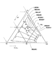
前記混酸の組成範囲が、これらの組成を重量%で表わす三角図において、
前記フッ酸が2.82重量%、前記硝酸が0.18重量%、前記硫酸が97重量%である点Aと、
前記フッ酸が0.18重量%、前記硝酸が2.82重量%、前記硫酸が97重量%である点Bと、
前記フッ酸が8.47重量%、前記硝酸が0.53重量%、前記硫酸が91重量%である点Cと、
前記フッ酸が0.53重量%、前記硝酸が8.47重量%、前記硫酸が91重量%である点Dと
をこの順で結ぶ4本の線分で囲まれた領域内にあり、
前記エッチング液の水の濃度が0〜10.5重量%である
太陽電池用シリコンウエハーの製造方法であることにある。
That is, the gist of the present invention is a method for producing a silicon wafer for solar cells, in which a slice of polycrystalline silicon is etched with an etchant containing a mixed acid as a main component,
The slice piece is a slice piece sliced with a fixed abrasive grain type wire saw,
The mixed acid comprises hydrofluoric acid represented by the chemical formula HF, nitric acid represented by the chemical formula HNO 3 and sulfuric acid represented by the chemical formula H 2 SO 4 ;
In the triangular diagram in which the composition range of the mixed acid represents these compositions in weight%,
Point A, in which the hydrofluoric acid is 2.82% by weight, the nitric acid is 0.18% by weight, and the sulfuric acid is 97% by weight;
Point B where the hydrofluoric acid is 0.18% by weight, the nitric acid is 2.82% by weight, and the sulfuric acid is 97% by weight;
Point C, where the hydrofluoric acid is 8.47 wt%, the nitric acid is 0.53% wt, and the sulfuric acid is 91 wt%;
The hydrofluoric acid is in a region surrounded by four line segments connecting the point D in which the hydrofluoric acid is 0.53% by weight, the nitric acid is 8.47% by weight, and the sulfuric acid is 91% by weight in this order;
It is in the manufacturing method of the silicon wafer for solar cells whose density | concentration of the water of the said etching liquid is 0 to 10.5 weight%.
前記太陽電池用シリコンウエハーの製造方法においては、前記スライス片がレジンボンドワイヤーソーでスライスされた多結晶シリコンウエハーである場合に特に低反射率で光沢ムラの少ない太陽電池用シリコンウエハーが得られる。
また、前記太陽電池用シリコンウエハーの製造方法により、表面に複数の略椀底形状の凹孔が全面にわたって形成されてなる凹凸を有し、前記凹孔の開口径が2〜15μmであり、かつ、各前記凹孔の内壁に開口径が0.1〜1.5μmの1または複数個の微孔が形成された、太陽電池用シリコンウエハーが得られる。
さらに、本発明の要旨とするところは、固定砥粒方式のワイヤーソーでスライスされた多結晶シリコンのスライス片のエッチングに用いるエッチング液であって、混酸を主成分とし、
前記混酸が、化学式HFで表わされるフッ酸、化学式HNO3で表わされる硝酸及び化学式H2SO4で表わされる硫酸からなり、
前記混酸の組成範囲が、これらの組成を重量%で表わす三角図において、
前記フッ酸が2.82重量%、前記硝酸が0.18重量%、前記硫酸が97重量%である点Aと、
前記フッ酸が0.18重量%、前記硝酸が2.82重量%、前記硫酸が97重量%である点Bと、
前記フッ酸が8.47重量%、前記硝酸が0.53重量%、前記硫酸が91重量%である点Cと、
前記フッ酸が0.53重量%、前記硝酸が8.47重量%、前記硫酸が91重量%である点Dと
をこの順で結ぶ4本の線分で囲まれた領域内にあり、
前記エッチング液の水の濃度が0〜10.5重量%であるエッチング液であることにある。前記エッチングする際のエッチング液の温度は0〜45℃である。
In the method for producing a silicon wafer for a solar cell, a silicon wafer for a solar cell with a low reflectance and less gloss unevenness can be obtained particularly when the slice piece is a polycrystalline silicon wafer sliced with a resin bond wire saw.
Further, according to the method for manufacturing a silicon wafer for a solar cell, the surface has a plurality of substantially bowl-shaped concave holes formed over the entire surface, the opening diameter of the concave holes is 2 to 15 μm, and A silicon wafer for solar cells is obtained in which one or a plurality of micropores having an opening diameter of 0.1 to 1.5 μm are formed on the inner wall of each concave hole.
Further, the gist of the present invention is an etching solution used for etching a slice piece of polycrystalline silicon sliced with a fixed abrasive grain type wire saw, having a mixed acid as a main component,
The mixed acid comprises hydrofluoric acid represented by the chemical formula HF, nitric acid represented by the chemical formula HNO 3 and sulfuric acid represented by the chemical formula H 2 SO 4 ;
In the triangular diagram in which the composition range of the mixed acid represents these compositions in weight%,
Point A, in which the hydrofluoric acid is 2.82% by weight, the nitric acid is 0.18% by weight, and the sulfuric acid is 97% by weight;
Point B where the hydrofluoric acid is 0.18% by weight, the nitric acid is 2.82% by weight, and the sulfuric acid is 97% by weight;
Point C, where the hydrofluoric acid is 8.47 wt%, the nitric acid is 0.53% wt, and the sulfuric acid is 91 wt%;
The hydrofluoric acid is in a region surrounded by four line segments connecting the point D in which the hydrofluoric acid is 0.53% by weight, the nitric acid is 8.47% by weight, and the sulfuric acid is 91% by weight in this order;
It exists in the etching liquid whose density | concentration of the water of the said etching liquid is 0 to 10.5 weight%. The temperature of the etching solution during the etching is 0 to 45 ° C.
前記エッチング液においては、前記固定砥粒方式のワイヤーソーに用いるソーワイヤーがレジンボンドソーワイヤーであり得る。 In the etching solution, a saw wire used in the fixed abrasive grain type wire saw may be a resin bond saw wire.
本発明によれば多結晶シリコンインゴットを固定砥粒方式でスライスして得られるスライス片を用いて得られた低反射率で光沢ムラの少ない太陽電池用シリコンウエハーの製造方法が提供される。 Manufacturing method of the silicon wafer hard for small solar gloss unevenness is provided with a low reflectance obtained using the slices obtained by slicing a polycrystalline silicon ingot according to the present invention with the fixed abrasive grain system .
太陽電池用シリコンウエハーは、多結晶シリコンインゴットを固定砥粒方式でスライスして得られるスライス片をエッチング液でエッチングして得られる。
A silicon wafer for solar cells is obtained by etching a slice piece obtained by slicing a polycrystalline silicon ingot by a fixed abrasive method with an etching solution.
固定砥粒方式は、芯線表面に砥粒を接着固定したソーワイヤーを用いてインゴットをスライスする方式であり、芯線表面に砥粒を接着固定する態様としては、溶融金属方式、電着方式、レジンボンド方式が挙げられる。 The fixed abrasive method is a method of slicing an ingot using a saw wire in which abrasive grains are bonded and fixed to the surface of the core wire. As an aspect of bonding and fixing the abrasive particles to the surface of the core wire, a molten metal method, an electrodeposition method, a resin Bond method is mentioned.
溶融金属方式は芯線表面に半田合金等の低融点金属(ろう材)を介して砥粒を固定する方式であり、特開2010−201602に記載の方式が例示される。 The molten metal method is a method in which abrasive grains are fixed to the surface of the core wire via a low melting point metal (brazing material) such as a solder alloy, and a method described in JP 2010-201602 A is exemplified.
電着方式は、砥粒を混合したメッキ液を用いて芯線表面にメッキ層を形成することにより、芯線表面にメッキ層を介して砥粒を固定する方式であり、特開2003−340729に記載の方式が例示される。 The electrodeposition method is a method in which a plating layer is formed on the surface of the core wire by using a plating solution mixed with abrasive particles, thereby fixing the abrasive particles on the surface of the core wire via the plating layer, as described in JP-A-2003-340729. This method is exemplified.
レジンボンド方式は芯線表面に砥粒を樹脂接着剤を介して固定する方式である。 The resin bond method is a method in which abrasive grains are fixed to the surface of the core wire through a resin adhesive.
固定砥粒方式において用いられる芯線としては鋼線が好ましく用いられる。線径は特に限定されないが0.3〜0.05mmのものが好ましい。鋼線には、高炭素鋼や中炭素低合金鋼などの熱処理バネ鋼による線材、硬鋼線、ピアノ線やステンレス線、冷間圧延鋼線やオイルテンパー線などの加工バネ鋼による線材、低合金鋼、中合金鋼や高合金鋼、マルエージング鋼などの高靭性・高疲労強度の鋼線材が挙げられる。 A steel wire is preferably used as the core wire used in the fixed abrasive system. The wire diameter is not particularly limited, but is preferably 0.3 to 0.05 mm. Steel wire includes heat-treated spring steel wire such as high carbon steel and medium carbon low alloy steel, hard steel wire, piano wire and stainless steel wire, cold rolled steel wire and oil tempered wire wire made of spring steel, low Examples include steel wires with high toughness and high fatigue strength such as alloy steel, medium alloy steel, high alloy steel, and maraging steel.
固定砥粒方式において用いられる砥粒としては特に限定されないが、ダイヤモンド砥粒、立方晶系BN砥粒、アルミナ砥粒、炭化珪素砥粒などが例示される。ダイヤモンド砥粒がニッケル被覆されたものであってもよい。なかでも、粒径5〜15μmのダイヤモンド砥粒を用いることが好ましい Although it does not specifically limit as an abrasive grain used in a fixed abrasive system, A diamond abrasive grain, cubic-type BN abrasive grain, an alumina abrasive grain, a silicon carbide abrasive grain etc. are illustrated. The diamond abrasive grains may be nickel-coated. Among them, it is preferable to use diamond abrasive grains having a particle diameter of 5 to 15 μm.
本発明においては、多結晶シリコンインゴットを固定砥粒方式でスライスして得られるスライス片をエッチング液を用いてエッチングすることにより、太陽電池用シリコンウエハーが製造される。 In the present invention, a silicon wafer for a solar cell is manufactured by etching a slice piece obtained by slicing a polycrystalline silicon ingot by a fixed abrasive method using an etching solution.
本発明において用いられるエッチング液は、フッ酸(HF)、硝酸(HNO3)及び硫酸(H2SO4)からなる混酸を主成分とする。このエッチング液はさらに水を含むことができる。 The etching solution used in the present invention contains a mixed acid composed of hydrofluoric acid (HF), nitric acid (HNO 3 ), and sulfuric acid (H 2 SO 4 ) as a main component. This etchant may further contain water.
また、このエッチング液は脂肪族カルボン酸、脂肪族スルホン酸、脂肪族リン酸などの有機酸や、過塩素酸、過塩素酸塩、過クロム酸、過クロム酸塩などの酸化剤を助剤として含んでいてもよい。また、硝酸ナトリウム、硝酸カリウム、硝酸アンモニウムなどの硝酸塩、亜硝酸ナトリウム、亜硝酸カリウム、亜硝酸アンモニウムなどの亜硝酸塩、フッ化ナトリウム、フッ化カリウム、フッ化アンモニウムなどのフッ化物塩を含んでいてもよい。 This etchant also aids organic acids such as aliphatic carboxylic acids, aliphatic sulfonic acids and aliphatic phosphoric acids, and oxidizing agents such as perchloric acid, perchlorate, perchromic acid and perchromate. May be included. Further, nitrates such as sodium nitrate, potassium nitrate and ammonium nitrate, nitrites such as sodium nitrite, potassium nitrite and ammonium nitrite, and fluoride salts such as sodium fluoride, potassium fluoride and ammonium fluoride may be contained.
本発明において用いられるエッチング液におけるフッ酸、硝酸、硫酸からなる混酸の、これらの酸の合計重量に対するそれぞれの酸の配合比率は、図1に示す三角図における点
A(HF:2.82重量%、HNO3:0.18重量%、H2SO4:97重量%)、
B(HF:0.18重量%、HNO3:2.82重量%、H2SO4:97重量%)、
C(HF:8.47重量%、HNO3:0.53重量%、H2SO4:91重量%)、
D(HF:0.53重量%、HNO3:8.47重量%、H2SO4:91重量%)
を結ぶ線分で囲まれた範囲内にある。
In the etching solution used in the present invention, the mixing ratio of each acid of the mixed acid composed of hydrofluoric acid, nitric acid, and sulfuric acid with respect to the total weight of these acids is point A (HF: 2.82 weight in the triangular diagram shown in FIG. %, HNO 3 : 0.18 wt%, H 2 SO 4 : 97 wt%),
B (HF: 0.18 wt%, HNO 3: 2.82 wt%,
C (HF: 8.47% by weight, HNO 3 : 0.53% by weight, H 2 SO 4 : 91% by weight),
D (HF: 0.53% by weight, HNO 3 : 8.47% by weight, H 2 SO 4 : 91% by weight)
It is in the range surrounded by the line segment connecting.
エッチング液の水分濃度(水を含む全成分を含めたエッチング液中の重量濃度、すなわち、水の含有比率)は0〜10.5重量%である。水分濃度がこれより高いと小凹(小さな窪み)が形成され難くなり、反射率が十分に下がらずに、かつ、ウエハーの結晶粒コントラスト差が顕著になる。エッチング液の水分濃度は10重量%以下であることがエッチング工程の安定性のうえでさらに好ましい。 The moisture concentration of the etching solution (weight concentration in the etching solution including all components including water, that is, the content ratio of water) is 0 to 10.5% by weight. If the moisture concentration is higher than this, it becomes difficult to form small concaves (small dents), the reflectance is not sufficiently lowered, and the crystal grain contrast difference of the wafer becomes remarkable. In view of stability of the etching process, the moisture concentration of the etching solution is more preferably 10% by weight or less.
エッチングは、多結晶シリコンインゴットを固定砥粒方式でスライスして得られるスライス片をエッチング液に浸漬することにより行われ、その後このスライス片を水洗する。浸漬における液温は0〜45℃、時間は1〜30分であることが好ましい。液温がこの範囲を下回ると、エッチングの進行が不十分であり、凹凸が形成されるまでの時間がかかり過ぎる。液温がこの範囲を上回ると、凹凸が、特に小凹が形成され難くなり、反射率が十分に下がらずに、かつ、結晶粒コントラスト差が顕著になり光沢にコントラスト差が出て商品価値が落ちる。従って、液温は5〜40℃であることがさらに好ましい。 Etching is performed by immersing a slice piece obtained by slicing a polycrystalline silicon ingot by a fixed abrasive method in an etching solution, and then washing the slice piece with water. It is preferable that the liquid temperature in immersion is 0 to 45 ° C. and the time is 1 to 30 minutes. When the liquid temperature falls below this range, the etching proceeds insufficiently and it takes too much time until the irregularities are formed. If the liquid temperature exceeds this range, it will be difficult to form irregularities, especially small depressions, the reflectivity will not be lowered sufficiently, and the difference in crystal grain contrast will be significant, resulting in a contrast difference in gloss and commercial value. drop down. Therefore, the liquid temperature is more preferably 5 to 40 ° C.
このエッチング液において、フッ酸、硝酸、硫酸の組成比率が図1に示す三角図における点ABCDを結ぶ線分で囲まれた範囲外であると、エッチング速度が遅くなりすぎて、エッチング反応が進まないため、凹凸が形成されるまでの時間がかかり過ぎる。あるいは、小凹が形成され難くなり、反射率が十分に下がらずに、かつ結晶粒コントラストが顕著になる。 In this etching solution, if the composition ratio of hydrofluoric acid, nitric acid, and sulfuric acid is outside the range surrounded by the line segment connecting the points ABCD in the triangular diagram shown in FIG. 1, the etching rate becomes too slow and the etching reaction proceeds. Therefore, it takes too much time until the irregularities are formed. Alternatively, it becomes difficult to form small concaves, the reflectance is not sufficiently lowered, and the crystal grain contrast becomes remarkable.
また、このエッチング液において、フッ酸の濃度/(フッ酸の濃度+硝酸の濃度)の値は0.059〜0.94であることが好ましい。この範囲外ではエッチング速度が下がるとともに、小凹が形成されにくくなり、反射率が上がり、また結晶粒コントラスト差が顕著になることがある。 In this etching solution, the concentration of hydrofluoric acid / (concentration of hydrofluoric acid + concentration of nitric acid) is preferably 0.059 to 0.94. Outside this range, the etching rate decreases, small cavities are hardly formed, the reflectivity increases, and the crystal grain contrast difference may become significant.
また、このエッチング液において、硫酸濃度は91〜97重量%である。硫酸濃度がこの範囲を上回るとエッチング速度が遅くなりすぎて、エッチング反応が進まないため、凹凸が形成されるまでの時間がかかり過ぎる。範囲を下回ると小凹が形成され難くなり、反射率が十分に下がらずに、かつ、結晶粒コントラスト差が顕著になる。 In this etching solution, the sulfuric acid concentration is 91 to 97% by weight. If the sulfuric acid concentration exceeds this range, the etching rate becomes too slow and the etching reaction does not proceed, so it takes too much time for the unevenness to be formed. Below the range as small concave is hardly formed, without fall reflectance enough, and the crystal grains contrast difference becomes remarkable.
また、本発明において用いられるエッチング液におけるフッ酸、硝酸、硫酸の、これらの酸の合計重量に対するそれぞれの酸の配合比率は、図1に示す三角図における点
A´(HF:2.62重量%、HNO3:0.88重量%、H2SO4:96.5重量%)、
B´(HF:0.88重量%、HNO3:2.62重量%、H2SO4:96.5重量%)、
C´(HF:6.75重量%、HNO3:2.25重量%、H2SO4:91重量%)、
D´(HF:2.25重量%、HNO3:6.75重量%、H2SO4:91重量%)
を結ぶ線分で囲まれた範囲内にあることが低反射率で結晶粒コントラスト差に起因する光沢ムラの少ない太陽電池用シリコンウエハーを得るうえでさらに好ましい。
Further, the blending ratio of each of the hydrofluoric acid, nitric acid, and sulfuric acid in the etching solution used in the present invention with respect to the total weight of these acids is point A ′ (HF: 2.62 wt. %, HNO 3 : 0.88 wt%, H 2 SO 4 : 96.5 wt%),
B ′ (HF: 0.88 wt%, HNO 3 : 2.62 wt%, H 2 SO 4 : 96.5 wt%),
C ′ (HF: 6.75 wt%, HNO 3 : 2.25 wt%, H 2 SO 4 : 91 wt%),
D ′ (HF: 2.25 wt%, HNO 3 : 6.75 wt%, H 2 SO 4 : 91 wt%)
It is more preferable to obtain a silicon wafer for a solar cell having a low reflectivity and less gloss unevenness due to a difference in crystal grain contrast.
また、本発明において用いられるエッチング液におけるフッ酸、硝酸、硫酸の、これらの酸の合計重量に対するそれぞれの酸の配合比率は、図1に示す三角図における点
A´´(HF:1.98重量%、HNO3:1.52重量%、H2SO4:96.5重量%)、
B´´(HF:1.44重量%、HNO3:2.06重量%、H2SO4:96.5重量%)、
C´´(HF:5.09重量%、HNO3:3.91重量%、H2SO4:91重量%)、
D´´(HF:3.71重量%、HNO3:5.29重量%、H2SO4:91重量%)
を結ぶ線分で囲まれた範囲内にあることが低反射率で光沢ムラの少ない太陽電池用シリコンウエハーを得るうえで最も好ましい。
Further, the blending ratio of each of the hydrofluoric acid, nitric acid, and sulfuric acid in the etching solution used in the present invention with respect to the total weight of these acids is indicated by a point A ″ (HF: 1.98) in the triangular diagram shown in FIG. Wt%, HNO 3 : 1.52 wt%, H 2 SO 4 : 96.5 wt%),
B ″ (HF: 1.44 wt%, HNO 3 : 2.06 wt%, H 2 SO 4 : 96.5 wt%),
C ″ (HF: 5.09 wt%, HNO 3 : 3.91 wt%, H 2 SO 4 : 91 wt%),
D ″ (HF: 3.71 wt%, HNO 3 : 5.29 wt%, H 2 SO 4 : 91 wt%)
It is most preferable to obtain a silicon wafer for solar cells with low reflectance and less gloss unevenness within the range surrounded by the line segments connecting the two.
本発明において用いられるエッチング液は、例えば、濃度40〜55wt%、あるいはそれより高濃度のフッ酸の水溶液と、濃度59〜75wt%、あるいはそれより高濃度の硝酸の水溶液と、好ましくは濃度95〜98wt%の硫酸(濃度x%の酸は酸x重量部と水(100−x)重量部の混合物をいう)とを混合して得ることができる。 The etching solution used in the present invention is, for example, an aqueous solution of hydrofluoric acid having a concentration of 40 to 55 wt% or higher, an aqueous solution of nitric acid having a concentration of 59 to 75 wt% or higher, preferably a concentration of 95. 98 wt% of sulfuric acid (acid concentration x% refers to a mixture of acid x parts by weight of water (100-x) parts by weight) and can be a obtained by mixing.
このような配合比率のエッチング液により多結晶シリコンインゴットを固定砥粒方式でスライスして得られるスライス片をエッチングすると、図2(a)に示すように、加工変質層が除去されてシリコンの結晶粒がこのスライス片の表面に露出することによりスライス片の表面に凹凸が形成されるとともに、この表面がさらにエッチングされて椀底形状の窪みが形成され、また、この窪みに起因する凹凸よりさらに微細な凹凸が椀底形状の窪みの内面に形成される。これにより、表面の反射率が小さい太陽電池用シリコンウエハーが得られる。また、光沢ムラの少ない太陽電池用シリコンウエハーが得られる。 When a slice piece obtained by slicing a polycrystalline silicon ingot by the fixed abrasive method is etched with an etching solution having such a blending ratio, the work-affected layer is removed as shown in FIG. As the grains are exposed on the surface of the slice piece, irregularities are formed on the surface of the slice piece, and the surface is further etched to form a basal-shaped depression, and moreover than the irregularities caused by the depression. Fine irregularities are formed on the inner surface of the bowl-shaped depression. Thereby, the silicon wafer for solar cells with a small surface reflectance is obtained. Moreover, the silicon wafer for solar cells with little gloss unevenness is obtained.
図2(a)は、本発明により得られた太陽電池用シリコンウエハーの表面の凹凸状態の走査型電子顕微鏡撮像であり、図2(b)は、遊離砥粒方式で多結晶シリコンインゴットをスライスして得られたスライス片を従来のフッ酸および硝酸のみ混合エッチング液でエッチングして得られた太陽電池用シリコンウエハーの表面の凹凸状態の走査型電子顕微鏡撮像である。 FIG. 2 (a) is a scanning electron microscope image of the surface of the silicon wafer for solar cells obtained by the present invention, and FIG. 2 (b) is a slice of a polycrystalline silicon ingot by the free abrasive grain method. It is a scanning electron microscope image of the uneven | corrugated state of the surface of the silicon wafer for solar cells obtained by etching the slice piece obtained by making only the conventional hydrofluoric acid and nitric acid mixed etching liquid.
図2(a)に示す本発明により得られた太陽電池用シリコンウエハーは、表面に底部が曲面状の複数の凹孔が全面にわたって形成されてなる凹凸を有している。この凹孔の開口径は2〜15μmであり、かつ、この凹孔の内壁に開口径が0.1〜1.5μmの1または複数個の微孔が形成されている。すなわち、本発明の太陽電池用シリコンウエハーは、表面に複数の凹孔が全面にわたって形成されてなる凹凸を有し、この凹孔の開口径が2〜15μmであり、かつ、この凹孔の内壁に開口径が0.1〜1.5μmの1または複数個の微孔が形成された形状を実質的に有する。このような凹凸の性状は、走査型共焦点レーザー顕微鏡、あるいは特許第3810749号公報に記載の形状測定装置などによって確認することができる。 The silicon wafer for solar cells obtained by the present invention shown in FIG. 2 (a) has irregularities formed by forming a plurality of concave holes having a curved bottom surface on the entire surface. The opening diameter of the concave hole is 2 to 15 μm, and one or a plurality of micro holes having an opening diameter of 0.1 to 1.5 μm are formed on the inner wall of the concave hole. That is, the silicon wafer for solar cells of the present invention has irregularities formed by forming a plurality of concave holes over the entire surface, the opening diameter of the concave holes is 2 to 15 μm, and the inner wall of the concave holes Substantially has a shape in which one or a plurality of micropores having an opening diameter of 0.1 to 1.5 μm are formed. Such unevenness can be confirmed by a scanning confocal laser microscope or a shape measuring apparatus described in Japanese Patent No. 3810748.
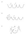
図3は、太陽電池用シリコンウエハーの表面の凹凸状態をウエハーの厚さ方向の切断面で示す模式図であり、図3(a)は図2(b)に示された太陽電池用シリコンウエハーの表面の凹凸状態、図3(b)は図2(a)に示された太陽電池用シリコンウエハーの表面の凹凸状態、図3(c)は図3(b)の部分拡大模式図である。図3(b)と図3(c)で示されるように本発明の太陽電池用シリコンウエハーは、拡大すると略椀の窪みの形状の大きな窪み(略椀底形状の凹孔)2に起因する大周期の凹凸(略椀底形状あるいは略椀底形状が重なった形状)に、エッチング液による浸食に起因する小さな窪み(微孔)3に起因する小周期の凹凸が重なった状態の凹凸を有する。大きな窪み2の上縁の径d1は2〜15μm、深さh1は2〜15μm、であり、小さな窪み3の上縁の径d2は0.1〜1.5μm、深さh2は0.1〜1.5μmである。また、互いに隣りあう大きな窪み2同士の、上縁の間隔pは0〜10μmである。また、1個の大きな窪み2の内面に複数個の小さな窪みが存在している。これに対して、図2(b)の顕微鏡撮像で示された、遊離砥粒方式で多結晶シリコンインゴットをスライスして得られたスライス片をエッチングして得られた太陽電池用シリコンウエハーの表面においては、大きな窪み2の内面に、図3(b)における小さな窪み3に相当する小さな窪みがほとんどない。また反射率は30%であり、本願エッチング液を用いた図2(a)と比較して十分に低い表面状態は形成され得なかった。
FIG. 3 is a schematic diagram showing the uneven state of the surface of the silicon wafer for solar cells by a cut surface in the thickness direction of the wafer. FIG. 3A is a silicon wafer for solar cells shown in FIG. 3B is a partially enlarged schematic view of FIG. 3B. FIG. 3B is a partially enlarged schematic view of the surface of the silicon wafer for solar cells shown in FIG. 2A. . As shown in FIGS. 3 (b) and 3 (c) , the silicon wafer for solar cells of the present invention, when enlarged, results from a large depression (substantially bowl-shaped recess) 2 having a substantially bowl-shaped depression. It has an irregularity in a state in which the irregularities of a small period caused by small depressions (micropores) 3 caused by erosion by the etching solution are superimposed on the irregularities of a large cycle (substantially basal shape or a shape in which the substantially basal shape overlaps). . The diameter d1 of the upper edge of the
なお、「全面にわたって」は、隣り合う凹孔のそれぞれの上縁部の間の間隔すなわちpが0〜10μmであるように凹孔がウエハーの表面に存在していることを意味する。また、隣り合う凹孔同士が互いに入りこんで重なってもよい。 “Over the entire surface” means that the concave holes are present on the surface of the wafer so that the distance between the upper edge portions of adjacent concave holes, that is, p is 0 to 10 μm. Moreover, adjacent concave holes may enter and overlap each other.
大きな窪み2は椀の窪みの形状に類似して、窪みの最深部からウエハーの面方向に垂直に立てた直線を対称の中心線として、あるいは窪みの最深部からウエハーの面方向に垂直に立てた平面を対称面として、略対称的な形状を有している。これはエッチングにより5μm程度の薄い加工変質層が除去されたうえにさらにエッチングがウエハーの厚さ方向に進行してこのような対称的な形状の窪みが形成されたことを示している。このような対称的な形状の窪みにより、ウエハー表面は不規則な反射光が生じにくく、光沢ムラの少ないウエハーを得ることができる。すなわち、本発明のエッチング液を用いたエッチングは、加工変質層の有無に依らずにエッチング行うことができる。従って、ウエハー表面には厚さ方向に関して対称的な形状の椀底形状の窪みが形成される。
The
本発明のエッチング液は加工変質層が除去されたあとのシリコンにあらためてこのような大きな窪み2と小さな窪み3とをともに形成できるエッチング液である。換言すれば、本発明のエッチング液は加工変質層の有無にかかわらずウエハー表面に大きな窪み2と小さな窪み3とをともに形成できるエッチング液である。
The etching solution of the present invention is an etching solution that can form both such a
これに対して、遊離砥粒方式で多結晶シリコンインゴットからスライスされたスライス片は、加工変質層が厚いので、エッチングによりこの加工変質層を除去するだけで表面に結晶粒に起因する凹凸が生ずることとなる。加工変質層の除去はフッ酸や硝酸を用いた従来のエッチング液を用いて比較的容易に行うことができる。しかし、このようにして得られた窪みは結晶粒の結晶方位に起因するので形状が不規則でウエハーの厚さ方向に関して非対称的な形状を有している。このため、ウエハー表面は不規則な反射光が生じやすく、光沢ムラの残ったウエハーが得られることとなる。このように、従来のエッチング液は加工変質層の除去の過程で凹凸を形成するものであり、加工変質層が除去されたあとのシリコンにあらためて凹凸を形成するものではない。また、従来のエッチング液では加工変質層が除去されたあとのシリコンにさらに小さな窪み3を形成するほどのエッチングを行うことが難しい。 On the other hand, since the sliced piece sliced from the polycrystalline silicon ingot by the free abrasive grain method has a thick work-affected layer, unevenness due to crystal grains is generated on the surface only by removing the work-affected layer by etching. It will be. The process-affected layer can be removed relatively easily using a conventional etching solution using hydrofluoric acid or nitric acid. However, the depressions obtained in this way are due to the crystal orientation of the crystal grains, and therefore have irregular shapes and asymmetric shapes with respect to the thickness direction of the wafer. For this reason, irregular reflected light tends to be generated on the wafer surface, and a wafer having gloss unevenness can be obtained. As described above, the conventional etching solution forms unevenness in the process of removing the work-affected layer, and does not form unevenness on the silicon after the work-affected layer is removed. In addition, it is difficult to perform etching to the extent that a smaller recess 3 is formed in silicon after the work-affected layer is removed with a conventional etching solution.
フッ酸、硝酸およびリン酸などを主成分とした酸性のエッチング液中で化学エッチングを行なうことによって、結晶面の不揃いな多結晶シリコンウエハーに関しても、10μmあるいはそれ以上の厚さの加工変質層をエッチング除去して凹凸を得る方法が開示されている(例えば、特開平10−303443号公報、特許第4766880号公報など)。
これは、以下の反応が進行するためとされている。
HNO3 + H2O + HNO2 → 2HNO2 + 2OH- + 2h+ (正孔)
Si + 4h+ → Si4+
Si4+ + 2OH- → SiO2 + H2
SiO2 +6HF → H2SiF6 + H2O
By performing chemical etching in an acidic etching solution mainly composed of hydrofluoric acid, nitric acid, phosphoric acid, etc., a work-affected layer having a thickness of 10 μm or more can be formed even for a polycrystalline silicon wafer having irregular crystal faces. A method for obtaining unevenness by etching removal is disclosed (for example, Japanese Patent Laid-Open No. 10-303443, Japanese Patent No. 4766880, etc.).
This is because the following reaction proceeds.
HNO 3 + H 2 O + HNO 2 →
Si + 4h + → Si 4+
Si 4+ + 2OH - → SiO 2 +
SiO 2 + 6HF → H 2 SiF 6 + H 2 O
従って、シリコンを酸化する硝酸とシリカ酸化物を溶解するフッ酸の割合に応じて、反応速度が変更できたり、凹凸の形状や大きさも変化するが、より安定した制御には、硫酸を系内に加えることが好ましい。この理由は以下のとおりである。 Therefore, depending on the ratio of nitric acid that oxidizes silicon and hydrofluoric acid that dissolves silica oxide, the reaction rate can be changed, and the shape and size of the unevenness can also be changed. It is preferable to add to. The reason for this is as follows.
つまり、シリコンの酸化反応は、上式の様に濃硝酸だけでも少しは反応するが、濃硫酸を加えると硫酸が酸で硝酸が塩基の酸・塩基反応が起こる。その結果,「-O-SO2-OH」アニオンと「H2O(+)-NO2」カチオンが形成され、「H2O(+)-NO2」カチオンから水が抜けて「(+)NO2」カチオン(ニトロニウム・カチオン)が系の中に多くなる。つまりは、下記反応式において平衡は濃硫酸を入れないときより右に偏ることになり、反応が速くなり、シリコン片の表面の凹凸形状を支配することになる。
2H2SO4 + HNO3 ⇔ NO2 + + H3O+ + 2HSO4 ー
このような現象に鑑み、本発明において、シリコン片の表面に良好な凹凸形状を形成するための酸の濃度、なかでも硫酸の濃度が見出された。
That is, the oxidation reaction of silicon reacts a little with concentrated nitric acid as shown above, but when concentrated sulfuric acid is added, an acid / base reaction in which sulfuric acid is an acid and nitric acid is a base occurs. As a result, the “—O—SO 2 —OH” anion and the “H 2 O (+)-NO 2 ” cation are formed, and the water is released from the “H 2 O (+)-NO 2 ” cation to “(+ ) NO 2 ”cation (nitronium cation) increases in the system. In other words, in the following reaction formula, the equilibrium is biased to the right as compared with when concentrated sulfuric acid is not added, the reaction becomes faster, and the surface roughness of the silicon piece is governed.
2H 2 SO 4 + HNO 3 ⇔ NO 2 + + H 3 O + +
In view of such a phenomenon, in the present invention, the concentration of acid for forming a good uneven shape on the surface of the silicon piece, in particular, the concentration of sulfuric acid was found.
以下に本発明の実施例を述べるが、本発明はこの実施例に限定されるものではない。 Examples of the present invention will be described below, but the present invention is not limited to these examples.
実施例、比較例におけるシリコンウエハーの反射率の測定は、島津製作所製紫外可視近赤外分光光度計Solidspec−3700と積分球BIS−3700を用いて行った。波長600nmの値の、9個所測定の平均値を求めて反射率とした。 In Examples and Comparative Examples, the reflectance of silicon wafers was measured using an ultraviolet-visible near-infrared spectrophotometer Solidspec-3700 and an integrating sphere BIS-3700 manufactured by Shimadzu Corporation. The average value of nine measurements at a wavelength of 600 nm was determined and used as the reflectance.
実施例1
<シリコンインゴット>
GET社製多結晶シリコンインゴットを用いた。
<ソーワイヤー>
株式会社TKX社製レジンボンドソーワイヤー(品番:MW−100−8−16)を用いた。
(レジンボンドソーワイヤー用の接着剤組成物・・・フェノール樹脂組成物
砥粒・・・ダイヤモンド砥粒:砥石径8−16μm(10.5μm±1μm)
ワイヤー・・・φ100μm鋼線)
<スライス工程>
周面に溝を切ったプーリーにソーワイヤーを巻回してループを形成する切断装置に装着し、600m/分の速度で走行させスライス片を得た。
<エッチング液>
フッ酸水溶液(濃度47wt%)・・・6.2重量%
硝酸水溶液(濃度67wt%)・・・5.0重量%
濃度95wt%の硫酸・・・88.8重量%
この組成は図1に実施例1の点として表示されている。
<エッチング>
スライス片を10℃のエッチング液に20分間浸漬後水洗してシリコンウエハーを得た。
<シリコンウエハーの特性>
得られたシリコンウエハーの反射率は18.6%であった。d1は3〜12μm(平均5.4μm)、d2は0.1〜1μmであった。図4(a)に示す表面状態の撮像のように、シリコンウエハーの表面に光沢ムラは殆んど認められなかった。なお、図2(a)は実施例1のシリコンウエハーの表面の凹凸の状態の顕微鏡撮像である。
Example 1
<Silicon ingot>
A polycrystalline silicon ingot manufactured by GET was used.
<Saw wire>
A resin bond saw wire (product number: MW-100-8-16) manufactured by TKX Corporation was used.
(Adhesive composition for resin bond saw wire: phenolic resin composition abrasive grains: diamond abrasive grains: grinding wheel diameter 8-16 μm (10.5 μm ± 1 μm)
Wire ... φ100μm steel wire)
<Slicing process>
A saw wire was wound around a pulley having a groove cut on its peripheral surface and attached to a cutting device for forming a loop. The slice was obtained by running at a speed of 600 m / min.
<Etching solution>
Hydrofluoric acid aqueous solution (concentration 47 wt%) ... 6.2 wt%
Nitric acid aqueous solution (concentration 67 wt%) ... 5.0 wt%
Sulfuric acid with a concentration of 95 wt% ... 88.8 wt%
This composition is displayed as the point of Example 1 in FIG.
<Etching>
The slice piece was immersed in an etching solution at 10 ° C. for 20 minutes and then washed with water to obtain a silicon wafer.
<Characteristics of silicon wafer>
The reflectance of the obtained silicon wafer was 18.6%. d1 was 3 to 12 μm (average 5.4 μm), and d2 was 0.1 to 1 μm. As in the imaging of the surface state shown in FIG. 4A, almost no gloss unevenness was observed on the surface of the silicon wafer. FIG. 2A is a microscopic image of the unevenness of the surface of the silicon wafer of Example 1. FIG.
実施例2
エッチング液の組成を
フッ酸水溶液(濃度47wt%)・・・6.3重量%
硝酸水溶液(濃度67wt%)・・・4.2重量%
濃度95wt%の硫酸・・・89.5重量%
とした他は実施例1と同様にしてシリコンウエハーを得た。
この組成は図1に実施例2の点として表示されている。
<シリコンウエハーの特性>
得られたシリコンウエハーの反射率は18.0%であった。d1は3〜10μm(平均4.8μm)、d2は0.1〜1μmであった。シリコンウエハーの表面に光沢ムラは全くといっていいほど認められなかった。
Example 2
The composition of the etching solution is hydrofluoric acid aqueous solution (concentration 47 wt%) ... 6.3 wt%
Nitric acid aqueous solution (concentration 67 wt%) ... 4.2 wt%
Sulfuric acid with a concentration of 95 wt% ... 89.5 wt%
A silicon wafer was obtained in the same manner as in Example 1 except that
This composition is displayed as the point of Example 2 in FIG.
<Characteristics of silicon wafer>
The reflectance of the obtained silicon wafer was 18.0%. d1 was 3 to 10 μm (average 4.8 μm), and d2 was 0.1 to 1 μm. There was almost no gloss unevenness on the surface of the silicon wafer.
実施例3
エッチング液の組成を
フッ酸水溶液(濃度47wt%)・・・6.6重量%
硝酸水溶液(濃度67wt%)・・・3.4重量%
濃度95wt%の硫酸・・・90重量%
とした他は実施例1と同様にしてシリコンウエハーを得た。
この組成は図1に実施例3の点として表示されている。
<シリコンウエハーの特性>
得られたシリコンウエハーの反射率は20.8%であった。d1は2〜8μm(平均3.9μm)、d2は0.1〜1μmであった。シリコンウエハーの表面に光沢ムラは全くといっていいほど認められなかった。
Example 3
The composition of the etching solution is a hydrofluoric acid aqueous solution (concentration 47 wt%)... 6.6 wt%
Nitric acid aqueous solution (concentration 67wt%) ... 3.4wt%
Sulfuric acid with a concentration of 95 wt.
A silicon wafer was obtained in the same manner as in Example 1 except that
This composition is displayed as the point of Example 3 in FIG.
<Characteristics of silicon wafer>
The reflectance of the obtained silicon wafer was 20.8%. d1 was 2 to 8 μm (average 3.9 μm), and d2 was 0.1 to 1 μm. There was almost no gloss unevenness on the surface of the silicon wafer.
実施例4
エッチング液の組成を
フッ酸水溶液(濃度47wt%)・・・6重量%
硝酸水溶液(濃度67wt%)・・・6重量%
濃度95wt%の硫酸・・・88重量%
とした他は実施例1と同様にしてシリコンウエハーを得た。
この組成は図1に実施例4の点として表示されている。
<シリコンウエハーの特性>
得られたシリコンウエハーの反射率は21.0%であった。d1は3〜10μm(平均3.9μm)、d2は0.1〜0.5μmであった。シリコンウエハーの表面に光沢ムラは若干認められたが、商品価値を損ねる程度ではなかった。
Example 4
The composition of the etching solution is a hydrofluoric acid aqueous solution (concentration 47 wt%) ... 6 wt%
Nitric acid aqueous solution (concentration 67 wt%) ... 6 wt%
Sulfuric acid with a concentration of 95 wt.
A silicon wafer was obtained in the same manner as in Example 1 except that
This composition is displayed as the point of Example 4 in FIG.
<Characteristics of silicon wafer>
The reflectance of the obtained silicon wafer was 21.0%. d1 was 3 to 10 μm (average 3.9 μm), and d2 was 0.1 to 0.5 μm. Although some uneven gloss was observed on the surface of the silicon wafer, it did not impair the commercial value.
実施例5
ソーワイヤーとして、特開2010−201602の実施例1に記載の方法により得られた、溶融金属方式によるソーワイヤーを用いたほかは実施例1と同様にしてシリコンウエハーを得た。
<ソーワイヤーの製造方法>
ワイヤーの金属製芯線は、真鍮によって被覆された線径φ100μmのピアノ線とした。
Example 5
A silicon wafer was obtained in the same manner as in Example 1 except that the saw wire obtained by the method described in Example 1 of JP2010-201602A was used as a saw wire.
<Saw wire manufacturing method>
The metal core wire of the wire was a piano wire with a wire diameter of φ100 μm covered with brass.
ろう材として、Sn−3.0%Ag−0.5%Cu(固相線:218℃、液相線:220℃)を用いた。これに、0.2%のアルミニウム(Al)粉末を添加し、溶融した。 As the brazing material, Sn-3.0% Ag-0.5% Cu (solidus: 218 ° C., liquidus: 220 ° C.) was used. To this, 0.2% aluminum (Al) powder was added and melted.
砥粒2としてニッケルが被覆されたダイヤモンドの粉末を用いた。砥粒の粒径は20〜35μmである。これを前述のろう材粉末とダイヤモンド粉末に対して有機アミン系活性ロジンフラックスを、70対30(重量%)の割合で混練し、ターピネオールによって粘度を300Pa・sに調整、これをペーストとしてディスペンサー(シリンジ)に充填した。
As the
ついで、100μmのノズル径をもつディスペンサーを用いて、ピアノ線芯材上に該ペーストを均質に22〜20μmの膜厚で塗布した。それを出力1W、ビーム径600〜1300μm、波長:808nmのレーザー光を照射することにより溶融し、その後自然冷却した。 Subsequently, using a dispenser having a nozzle diameter of 100 μm, the paste was uniformly applied to a piano wire core material with a film thickness of 22 to 20 μm. It was melted by irradiating it with laser light having an output of 1 W, a beam diameter of 600 to 1300 μm, and a wavelength of 808 nm, and then naturally cooled.
溶融状態を判断しながら、ダイヤモンドとろう材との割合は、溶融固化層の厚さが砥粒2の粒径の5〜40%におさまるように設定した。
While judging the melted state, the ratio of diamond to brazing material was set so that the thickness of the melt-solidified layer was 5 to 40% of the grain size of the
<シリコンウエハーの特性>
得られたシリコンウエハーの反射率は22.0%であった。d1は3〜14μm(平均4.0μm)、d2は0.1〜0.5μmであった。シリコンウエハーの表面に光沢ムラは若干認められたが、商品価値を損ねる程度ではなかった。
<Characteristics of silicon wafer>
The reflectance of the obtained silicon wafer was 22.0%. d1 was 3 to 14 μm (average 4.0 μm), and d2 was 0.1 to 0.5 μm. Although some uneven gloss was observed on the surface of the silicon wafer, it did not impair the commercial value.
実施例6
エッチング液の組成を
フッ酸水溶液(濃度47wt%)・・・4.2重量%
硝酸水溶液(濃度69wt%)・・・7.8重量%
濃度95wt%の硫酸・・・88.0重量%
とし、スライス片を25℃のエッチング液に142秒間浸漬後水洗してシリコンウエハーを得た。その他は実施例1と同様である。
この組成は図1に実施例6の点として表示されている。
<シリコンウエハーの特性>
得られたシリコンウエハーの反射率は23.0%であった。d1は2〜12μm(平均4.1μm)、d2は0.4〜1.0μmであった。シリコンウエハーの表面に、光沢ムラは若干認められたが、商品価値を損ねる程度ではなかった。
Example 6
The composition of the etching solution is hydrofluoric acid aqueous solution (concentration 47 wt%) ... 4.2 wt%
Nitric acid aqueous solution (concentration 69 wt%) 7.8 wt%
Sulfuric acid with a concentration of 95 wt% ... 88.0 wt%
Then, the slice piece was immersed in an etching solution at 25 ° C. for 142 seconds and then washed with water to obtain a silicon wafer. Others are the same as in the first embodiment.
This composition is displayed as the point of Example 6 in FIG.
<Characteristics of silicon wafer>
The reflectance of the obtained silicon wafer was 23.0%. d1 was 2 to 12 μm (average 4.1 μm), and d2 was 0.4 to 1.0 μm. Although some uneven gloss was observed on the surface of the silicon wafer, it did not impair the commercial value.
実施例7
エッチング液の組成を
フッ酸水溶液(濃度47wt%)・・・4.6重量%
硝酸水溶液(濃度69wt%)・・・6.9重量%
濃度95wt%の硫酸・・・88.5重量%
とし、スライス片を25℃のエッチング液に142秒間浸漬後水洗してシリコンウエハーを得た。その他は実施例1と同様である。
この組成は図1に実施例7の点として表示されている。
<シリコンウエハーの特性>
得られたシリコンウエハーの反射率は19.4%であった。d1は3〜8μm(平均4.8μm)、d2は0.4〜1.1μmであった。シリコンウエハーの表面に、光沢ムラは若干認められたが、商品価値を損ねる程度ではなかった。
Example 7
The composition of the etching solution is a hydrofluoric acid aqueous solution (concentration 47 wt%) ... 4.6 wt%
Nitric acid aqueous solution (concentration 69 wt%) ... 6.9 wt%
Sulfuric acid with a concentration of 95wt% ... 88.5wt%
Then, the slice piece was immersed in an etching solution at 25 ° C. for 142 seconds and then washed with water to obtain a silicon wafer. Others are the same as in the first embodiment.
This composition is displayed as the point of Example 7 in FIG.
<Characteristics of silicon wafer>
The reflectance of the obtained silicon wafer was 19.4%. d1 was 3 to 8 μm (average 4.8 μm), and d2 was 0.4 to 1.1 μm. Although some uneven gloss was observed on the surface of the silicon wafer, it did not impair the commercial value.
実施例8
エッチング液の組成を
フッ酸水溶液(濃度47wt%)・・・4.95重量%
硝酸水溶液(濃度69wt%)・・・6.05重量%
濃度95wt%の硫酸・・・89.0重量%
とし、スライス片を25℃のエッチング液に142秒間浸漬後水洗してシリコンウエハーを得た。その他は実施例1と同様である。
この組成は図1に実施例8の点として表示されている。
<シリコンウエハーの特性>
得られたシリコンウエハーの反射率は19.4%であった。d1は3〜10μm(平均6.5μm)、d2は0.5〜1.3μmであった。シリコンウエハーの表面に、光沢ムラは若干認められたが、商品価値を損ねる程度ではなかった。
Example 8
The composition of the etching solution is hydrofluoric acid aqueous solution (concentration 47 wt%) ... 4.95 wt%
Nitric acid aqueous solution (concentration 69 wt%) ... 6.05 wt%
Sulfuric acid with a concentration of 95 wt% ... 89.0 wt%
Then, the slice piece was immersed in an etching solution at 25 ° C. for 142 seconds and then washed with water to obtain a silicon wafer. Others are the same as in the first embodiment.
This composition is displayed as the point of Example 8 in FIG.
<Characteristics of silicon wafer>
The reflectance of the obtained silicon wafer was 19.4%. d1 was 3 to 10 μm (average 6.5 μm), and d2 was 0.5 to 1.3 μm. Although some uneven gloss was observed on the surface of the silicon wafer, it did not impair the commercial value.
実施例9
エッチング液の組成を
フッ酸水溶液(濃度47wt%)・・・5.25重量%
硝酸水溶液(濃度69wt%)・・・5.25重量%
濃度95wt%の硫酸・・・89.5重量%
とし、スライス片を25℃のエッチング液に142秒間浸漬後水洗してシリコンウエハーを得た。その他は実施例1と同様である。
この組成は図1に実施例9の点として表示されている。
<シリコンウエハーの特性>
得られたシリコンウエハーの反射率は19.8%であった。d1は3〜11μm(平均5.6μm)、d2は0.5〜1.1μmであった。シシリコンウエハーの表面に、光沢ムラはほぼ無かった。
Example 9
The composition of the etching solution is hydrofluoric acid aqueous solution (concentration 47 wt%) ... 5.25 wt%
Nitric acid aqueous solution (concentration 69 wt%) ... 5.25 wt%
Sulfuric acid with a concentration of 95 wt% ... 89.5 wt%
Then, the slice piece was immersed in an etching solution at 25 ° C. for 142 seconds and then washed with water to obtain a silicon wafer. Others are the same as in the first embodiment.
This composition is displayed as the point of Example 9 in FIG.
<Characteristics of silicon wafer>
The reflectance of the obtained silicon wafer was 19.8%. d1 was 3 to 11 μm (average 5.6 μm), and d2 was 0.5 to 1.1 μm. There was almost no uneven gloss on the surface of the silicon wafer.
比較例1
エッチング液の組成を
フッ酸水溶液(濃度47wt%)・・・4,5重量%
硝酸水溶液(濃度67wt%)・・・9重量%
濃度95wt%の硫酸・・・86.5重量%
とした他は実施例1と同様にしてシリコンウエハーを得た。
この組成は図1に比較例1の点として表示されている。
<シリコンウエハーの特性>
得られたシリコンウエハーの反射率は26.1%であった。d1は3〜15μm(平均5.1μm)、d2は0.1〜1μmであった。シリコンウエハーの表面に商品価値を損ねる程度の光沢ムラが認められた。図4(b)は得られたシリコンウエハーの光沢状態を示す撮像である。
Comparative Example 1
The composition of the etching solution is hydrofluoric acid aqueous solution (concentration 47 wt%) ... 4,5 wt%
Nitric acid aqueous solution (concentration 67 wt%) ... 9 wt%
Sulfuric acid with a concentration of 95 wt% ... 86.5 wt%
A silicon wafer was obtained in the same manner as in Example 1 except that
This composition is displayed as the point of Comparative Example 1 in FIG.
<Characteristics of silicon wafer>
The reflectance of the obtained silicon wafer was 26.1%. d1 was 3 to 15 μm (average 5.1 μm), and d2 was 0.1 to 1 μm. Gloss unevenness to the extent that the commercial value is impaired was observed on the surface of the silicon wafer. FIG. 4B is an image showing the gloss state of the obtained silicon wafer.
比較例2
エッチング液の組成を
フッ酸水溶液(濃度47wt%)・・・3.6重量%
硝酸水溶液(濃度67wt%)・・・16重量%
濃度95wt%の硫酸・・・80.4重量%
とした他は実施例1と同様にしてシリコンウエハーを得た。
<シリコンウエハーの特性>
得られたシリコンウエハーの反射率は27%であった。シリコンウエハーの表面に商品価値を損ねる程度の光沢ムラが認められた。
Comparative Example 2
The composition of the etching solution is a hydrofluoric acid aqueous solution (concentration 47 wt%)... 3.6 wt%
Nitric acid aqueous solution (concentration 67wt%) ... 16wt%
95wt% sulfuric acid concentration 80.4wt%
A silicon wafer was obtained in the same manner as in Example 1 except that
<Characteristics of silicon wafer>
The reflectance of the obtained silicon wafer was 27%. Gloss unevenness to the extent that the commercial value is impaired was observed on the surface of the silicon wafer.
比較例3
エッチング液の組成を
フッ酸水溶液(濃度47wt%)・・・6重量%
硝酸水溶液(濃度67wt%)・・・29重量%
濃度95wt%の硫酸・・・65重量%
とした他は実施例1と同様にしてシリコンウエハーを得た。
<シリコンウエハーの特性>
得られたシリコンウエハーの反射率は30%であった。シリコンウエハーの表面に商品価値を大きく損ねる程度の光沢ムラが認められた。
Comparative Example 3
The composition of the etching solution is a hydrofluoric acid aqueous solution (concentration 47 wt%) ... 6 wt%
Nitric acid aqueous solution (concentration 67 wt%) ... 29 wt%
95% by weight sulfuric acid ... 65% by weight
A silicon wafer was obtained in the same manner as in Example 1 except that
<Characteristics of silicon wafer>
The reflectance of the obtained silicon wafer was 30%. Gloss unevenness to the extent that the commercial value is greatly impaired was observed on the surface of the silicon wafer.
比較例4
<スライス工程>
遊離砥粒方式のマルチワイヤーソー方式を用いて、実施例1に用いたと同様のインゴットをスライスした。
ワイヤー直径 :0.1mm(JFEスチール社製、型式SRH)
砥粒: 炭化ケイ素
(フジミインコーポレーテッド社製、GC#1500、平均粒子径約8μm)
切断速度 :0.35mm/分(インゴット送り速度)
ワイヤー走行速度:600m/分
<エッチング>
エッチング液の組成を
フッ酸水溶液(濃度47wt%)・・・25重量%
硝酸水溶液(濃度67wt%)・・・45重量%
水・・・30重量%
とした他は実施例1と同様のエッチングによりシリコンウエハーを得た。ただし、エッチングは10℃×2分で行った。
<シリコンウエハーの特性>
d1は平均10μmであり、大きな窪み2のみ認められ、小さな窪み3は認められなかった。このため得られたシリコンウエハーの反射率は30.8%と高いままであった。図4(c)はこのシリコンウエハーの光沢状態を示す撮像である。
Comparative Example 4
<Slicing process>
An ingot similar to that used in Example 1 was sliced using a multi-wire saw method of loose abrasive grains.
Wire diameter: 0.1 mm (manufactured by JFE Steel, model SRH)
Abrasive grains: Silicon carbide (manufactured by Fujimi Incorporated, GC # 1500, average particle diameter of about 8 μm)
Cutting speed: 0.35 mm / min (ingot feed speed)
Wire traveling speed: 600m / min <etching>
The composition of the etching solution is hydrofluoric acid aqueous solution (concentration 47 wt%) ... 25 wt%
Nitric acid aqueous solution (concentration 67 wt%) 45% by weight
Water ... 30% by weight
A silicon wafer was obtained by the same etching as in Example 1 except that. However, etching was performed at 10 ° C. × 2 minutes.
<Characteristics of silicon wafer>
d1 was 10 μm on average, and only the
比較例5
エッチング液の組成を
フッ酸水溶液(濃度47wt%)・・・25重量%
硝酸水溶液(濃度67wt%)・・・45重量%
水・・・30重量%
とした他は実施例1と同様にしてシリコンウエハーを得た。ただし、エッチングは10℃×2分で行った。
<シリコンウエハーの特性>
得られたシリコンウエハーの反射率は32.5%と高い値であった。図2(c)はこのシリコンウエハーの表面の凹凸の状態の顕微鏡撮像であり、図4(d)はこのシリコンウエハーの光沢状態を示す撮像である。d1は3〜15μm(平均5.5μm)であったが、小さな窪み3は認められなかった。また、シリコンウエハーの表面に商品価値を損ねる程度の光沢ムラが認められた。
得られたシリコンウエハーの反射率は32.5%であった。
Comparative Example 5
The composition of the etching solution is hydrofluoric acid aqueous solution (concentration 47 wt%) ... 25 wt%
Nitric acid aqueous solution (concentration 67 wt%) 45% by weight
Water ... 30% by weight
A silicon wafer was obtained in the same manner as in Example 1 except that However, etching was performed at 10 ° C. × 2 minutes.
<Characteristics of silicon wafer>
The reflectance of the obtained silicon wafer was as high as 32.5%. FIG. 2C is a microscopic image of the surface irregularity of the silicon wafer, and FIG. 4D is an image showing the glossy state of the silicon wafer. d1 was 3 to 15 μm (average 5.5 μm), but no small depression 3 was observed. Further, gloss unevenness to the extent that the commercial value was impaired was observed on the surface of the silicon wafer.
The reflectance of the obtained silicon wafer was 32.5%.
本発明は、太陽電池用シリコンウエハーや、その他の光電変換素子の製造に広く適用できる有益な技術である。 The present invention is a useful technique that can be widely applied to the manufacture of silicon wafers for solar cells and other photoelectric conversion elements.
2:大きな窪み
3:小さな窪み
2: Large depression 3: Small depression
Claims (3)
前記混酸が、化学式HFで表わされるフッ酸、化学式HNO3で表わされる硝酸及び化学式H2SO4で表わされる硫酸からなり、
前記混酸の組成範囲が、これらの組成を重量%で表わす三角図において、
前記フッ酸が2.82重量%、前記硝酸が0.18重量%、前記硫酸が97重量%である点Aと、
前記フッ酸が0.18重量%、前記硝酸が2.82重量%、前記硫酸が97重量%である点Bと、
前記フッ酸が8.47重量%、前記硝酸が0.53重量%、前記硫酸が91重量%である点Cと、
前記フッ酸が0.53重量%、前記硝酸が8.47重量%、前記硫酸が91重量%である点Dと
をこの順で結ぶ4本の線分で囲まれた領域内にあり、
前記エッチング液の水の濃度が0〜10.5重量%であり、
前記固定砥粒方式のワイヤーソーでスライスして多結晶シリコンのスライス片を得て、該スライス片を前記エッチング液でエッチングすることにより、表面に複数の略椀底形状の凹孔が全面にわたって形成されてなる凹凸を有し、前記凹孔の開口径が2〜15μmであり、かつ、各前記凹孔の内壁に開口径が0.1〜1.5μmの1または複数個の微孔を形成する
太陽電池用シリコンウエハーの製造方法。 A method for producing a silicon wafer for a solar cell, comprising slicing polycrystalline silicon with a fixed-abrasive wire saw to obtain a slice piece, and etching the slice piece with an etchant containing a mixed acid as a main component,
The mixed acid comprises hydrofluoric acid represented by the chemical formula HF, nitric acid represented by the chemical formula HNO 3 and sulfuric acid represented by the chemical formula H 2 SO 4 ;
In the triangular diagram in which the composition range of the mixed acid represents these compositions in weight%,
Point A, in which the hydrofluoric acid is 2.82% by weight, the nitric acid is 0.18% by weight, and the sulfuric acid is 97% by weight;
Point B where the hydrofluoric acid is 0.18% by weight, the nitric acid is 2.82% by weight, and the sulfuric acid is 97% by weight;
Point C, where the hydrofluoric acid is 8.47 wt%, the nitric acid is 0.53% wt, and the sulfuric acid is 91 wt%;
The hydrofluoric acid is in a region surrounded by four line segments connecting the point D in which the hydrofluoric acid is 0.53% by weight, the nitric acid is 8.47% by weight, and the sulfuric acid is 91% by weight;
The water concentration of the etching solution is 0 to 10.5% by weight,
A sliced piece of polycrystalline silicon is obtained by slicing with the fixed abrasive grain type wire saw , and by etching the slice piece with the etching solution, a plurality of substantially bowl-shaped concave holes are formed on the entire surface. 1 or a plurality of micro holes having an opening diameter of 2 to 15 μm and an opening diameter of 0.1 to 1.5 μm are formed on the inner wall of each of the recessed holes. To manufacture a silicon wafer for solar cells.
Priority Applications (6)
| Application Number | Priority Date | Filing Date | Title |
|---|---|---|---|
| JP2014009159A JP5868437B2 (en) | 2013-04-26 | 2014-01-22 | Method for producing silicon wafer for solar cell |
| SG11201508619VA SG11201508619VA (en) | 2013-04-26 | 2014-04-09 | Silicon wafer for solar cells and method for producing same |
| PCT/JP2014/060349 WO2014175072A1 (en) | 2013-04-26 | 2014-04-09 | Silicon wafer for solar cells and method for producing same |
| CN201480023748.1A CN105144351B (en) | 2013-04-26 | 2014-04-09 | Silicon for solar cell wafer and its manufacture method |
| KR1020157022409A KR20160002683A (en) | 2013-04-26 | 2014-04-09 | Silicon wafer for solar cells and method for producing same |
| TW103114268A TW201444955A (en) | 2013-04-26 | 2014-04-18 | Silicon wafer for solar cells and method for producing same |
Applications Claiming Priority (3)
| Application Number | Priority Date | Filing Date | Title |
|---|---|---|---|
| JP2013094163 | 2013-04-26 | ||
| JP2013094163 | 2013-04-26 | ||
| JP2014009159A JP5868437B2 (en) | 2013-04-26 | 2014-01-22 | Method for producing silicon wafer for solar cell |
Publications (3)
| Publication Number | Publication Date |
|---|---|
| JP2014225633A JP2014225633A (en) | 2014-12-04 |
| JP2014225633A5 JP2014225633A5 (en) | 2015-07-16 |
| JP5868437B2 true JP5868437B2 (en) | 2016-02-24 |
Family
ID=51791652
Family Applications (1)
| Application Number | Title | Priority Date | Filing Date |
|---|---|---|---|
| JP2014009159A Expired - Fee Related JP5868437B2 (en) | 2013-04-26 | 2014-01-22 | Method for producing silicon wafer for solar cell |
Country Status (6)
| Country | Link |
|---|---|
| JP (1) | JP5868437B2 (en) |
| KR (1) | KR20160002683A (en) |
| CN (1) | CN105144351B (en) |
| SG (1) | SG11201508619VA (en) |
| TW (1) | TW201444955A (en) |
| WO (1) | WO2014175072A1 (en) |
Families Citing this family (6)
| Publication number | Priority date | Publication date | Assignee | Title |
|---|---|---|---|---|
| JP2014232829A (en) * | 2013-05-30 | 2014-12-11 | 日本化成株式会社 | Method for manufacturing silicon wafer for solar batteries |
| JP6898737B2 (en) * | 2014-12-15 | 2021-07-07 | シャープ株式会社 | Manufacturing method of semiconductor substrate, manufacturing method of photoelectric conversion element and photoelectric conversion element |
| TWI538986B (en) * | 2015-07-15 | 2016-06-21 | 綠能科技股份有限公司 | Etching solution and method of surface roughening of silicon substrate |
| JP6885942B2 (en) * | 2015-11-23 | 2021-06-16 | インテグリス・インコーポレーテッド | Compositions and Methods for Selectively Etching P-Type Doped polysilicon Compared to Silicon Nitride |
| CN108183067A (en) * | 2018-01-05 | 2018-06-19 | 苏州同冠微电子有限公司 | A kind of processing method of semiconductor crystal wafer |
| CN111748806B (en) * | 2020-07-21 | 2022-08-23 | 江苏悦锌达新材料有限公司 | Roughening liquid for polyphenylene sulfide and composite material thereof, preparation method and use method thereof |
Family Cites Families (20)
| Publication number | Priority date | Publication date | Assignee | Title |
|---|---|---|---|---|
| JPH09270400A (en) | 1996-01-31 | 1997-10-14 | Shin Etsu Handotai Co Ltd | Method of manufacturing semiconductor wafer |
| JP4024934B2 (en) | 1998-08-10 | 2007-12-19 | 住友電気工業株式会社 | Wire saw and manufacturing method thereof |
| DE19962136A1 (en) * | 1999-12-22 | 2001-06-28 | Merck Patent Gmbh | Etching mixture used in production of structured surfaces on multi-crystalline, tri-crystalline and monocrystalline silicon surfaces of solar cells contains hydrofluoric acid and mineral acids selected from nitric acid |
| EP1295320A2 (en) | 2000-06-30 | 2003-03-26 | MEMC Electronic Materials, Inc. | Process for etching silicon wafers |
| JP2004063954A (en) | 2002-07-31 | 2004-02-26 | Sumitomo Mitsubishi Silicon Corp | Etching method of silicon wafer, and method of differentiating front and rear faces of silicon wafer using the etching method |
| JP3870896B2 (en) * | 2002-12-11 | 2007-01-24 | 株式会社デンソー | Semiconductor device manufacturing method and semiconductor device manufactured thereby |
| WO2005036629A1 (en) | 2003-10-10 | 2005-04-21 | Mimasu Semiconductor Industry Co., Ltd. | Process for roughening surface of wafer |
| JP4430488B2 (en) | 2004-09-02 | 2010-03-10 | シャープ株式会社 | Solar cell and manufacturing method thereof |
| JP4766880B2 (en) * | 2005-01-18 | 2011-09-07 | シャープ株式会社 | Crystal silicon wafer, crystal silicon solar cell, method for manufacturing crystal silicon wafer, and method for manufacturing crystal silicon solar cell |
| US8222118B2 (en) * | 2008-12-15 | 2012-07-17 | Intel Corporation | Wafer backside grinding with stress relief |
| KR20120135185A (en) * | 2009-09-21 | 2012-12-12 | 바스프 에스이 | Acqueous acidic etching solution and method for texturing the surface of single crystal and polycrystal silicon substrates |
| DE102010012044A1 (en) * | 2010-03-19 | 2011-09-22 | Friedrich-Schiller-Universität Jena | Structured silicon layer for e.g. silicon solar cell, has boundary surface with bent partial surfaces exhibiting nano-structure that is extended into layer upto depth between four hundred nanometer and five micrometer |
| JP2011255475A (en) | 2010-06-11 | 2011-12-22 | Takatori Corp | Fixed abrasive wire |
| JP2012024866A (en) | 2010-07-21 | 2012-02-09 | Sumco Corp | Method of collecting wire saw cutting sludge and device therefor |
| KR101657626B1 (en) * | 2010-10-08 | 2016-09-19 | 주식회사 원익아이피에스 | Method for manufacturing solar cell and solar cell manufactured by the same method |
| JP5677469B2 (en) * | 2011-01-27 | 2015-02-25 | 京セラ株式会社 | Method for manufacturing solar cell element, solar cell element, and solar cell module |
| JP2012169420A (en) * | 2011-02-14 | 2012-09-06 | Sumco Corp | Solar cell wafer manufacturing method, solar cell manufacturing method and solar cell module manufacturing method |
| JP2012222300A (en) * | 2011-04-13 | 2012-11-12 | Panasonic Corp | Silicon substrate including texture formation surface, and manufacturing method of the same |
| JP5780856B2 (en) | 2011-06-30 | 2015-09-16 | 京セラ株式会社 | Multilayer ceramic capacitor |
| JP2013043268A (en) | 2011-08-26 | 2013-03-04 | Sharp Corp | Fixed abrasive grain wire and method of manufacturing semiconductor substrate |
-
2014
- 2014-01-22 JP JP2014009159A patent/JP5868437B2/en not_active Expired - Fee Related
- 2014-04-09 WO PCT/JP2014/060349 patent/WO2014175072A1/en active Application Filing
- 2014-04-09 CN CN201480023748.1A patent/CN105144351B/en not_active Expired - Fee Related
- 2014-04-09 KR KR1020157022409A patent/KR20160002683A/en not_active Application Discontinuation
- 2014-04-09 SG SG11201508619VA patent/SG11201508619VA/en unknown
- 2014-04-18 TW TW103114268A patent/TW201444955A/en unknown
Also Published As
| Publication number | Publication date |
|---|---|
| TW201444955A (en) | 2014-12-01 |
| CN105144351B (en) | 2017-09-26 |
| CN105144351A (en) | 2015-12-09 |
| KR20160002683A (en) | 2016-01-08 |
| WO2014175072A1 (en) | 2014-10-30 |
| SG11201508619VA (en) | 2015-12-30 |
| JP2014225633A (en) | 2014-12-04 |
Similar Documents
| Publication | Publication Date | Title |
|---|---|---|
| JP5868437B2 (en) | Method for producing silicon wafer for solar cell | |
| CN101621026B (en) | Back laser cutting method of glass passivated silicon wafer | |
| TWI494416B (en) | Acidic etching solution and method for texturing the surface of single crystal and polycrystal silicon substrates | |
| US9876128B2 (en) | Texturing monocrystalline silicon substrates | |
| JP2012230929A (en) | Solar cell silicon wafer and manufacturing method thereof | |
| TWI510682B (en) | Modification process for nano-structuring ingot surface, wafer manufacturing method and wafer thereof | |
| US20090042390A1 (en) | Etchant for silicon wafer surface shape control and method for manufacturing silicon wafers using the same | |
| JP5509410B2 (en) | Method for manufacturing silicon substrate for solar cell | |
| CN109290874B (en) | Indium phosphide wafer with olive-shaped pits on back surface, preparation method and etching solution used by same | |
| US20160096248A1 (en) | Ingot and methods for ingot grinding | |
| JPH11171693A (en) | Etching of silicon wafer and etching liquid for silicon wafer | |
| CN109623676B (en) | Hub type diamond ultrathin cutting blade for PCB and application thereof | |
| CN207630298U (en) | A kind of ultra high efficiency multi-wire saw diamond wire | |
| CN103828064B (en) | Wafer used for solar batteries, the production method of wafer used for solar batteries, the production method of solaode and the production method of solar module | |
| CN207578758U (en) | A kind of diamond wire for multi-wire saw | |
| JP2005340643A (en) | Manufacturing method of semiconductor substrate for solar cell | |
| WO2018025539A1 (en) | Method for cutting silicon ingot, method for manufacturing silicon wafer, and silicon wafer | |
| EP2031101A2 (en) | Method for making silicon wafers | |
| WO2013080607A1 (en) | Method for recycling silicon offcuts, and purified product of same | |
| KR102255578B1 (en) | Method for wet two-step surface texturing of silicon wafer produced by kerfless | |
| JP2015145042A (en) | wire tool | |
| JP2014165385A (en) | Silicon substrate having texture structure, and method for manufacturing the same | |
| Coustier et al. | Diamond wire sawing: State of the art and perspectives | |
| JP2007175784A (en) | Wire saw device | |
| JPWO2013180221A1 (en) | Silicon wafer for solar cell and method for producing the same |
Legal Events
| Date | Code | Title | Description |
|---|---|---|---|
| A521 | Request for written amendment filed |
Free format text: JAPANESE INTERMEDIATE CODE: A523 Effective date: 20150528 |
|
| A621 | Written request for application examination |
Free format text: JAPANESE INTERMEDIATE CODE: A621 Effective date: 20150528 |
|
| A871 | Explanation of circumstances concerning accelerated examination |
Free format text: JAPANESE INTERMEDIATE CODE: A871 Effective date: 20150528 |
|
| A975 | Report on accelerated examination |
Free format text: JAPANESE INTERMEDIATE CODE: A971005 Effective date: 20150706 |
|
| A131 | Notification of reasons for refusal |
Free format text: JAPANESE INTERMEDIATE CODE: A131 Effective date: 20150713 |
|
| A521 | Request for written amendment filed |
Free format text: JAPANESE INTERMEDIATE CODE: A523 Effective date: 20150908 |
|
| A131 | Notification of reasons for refusal |
Free format text: JAPANESE INTERMEDIATE CODE: A131 Effective date: 20151112 |
|
| A521 | Request for written amendment filed |
Free format text: JAPANESE INTERMEDIATE CODE: A523 Effective date: 20151130 |
|
| TRDD | Decision of grant or rejection written | ||
| A01 | Written decision to grant a patent or to grant a registration (utility model) |
Free format text: JAPANESE INTERMEDIATE CODE: A01 Effective date: 20151217 |
|
| A61 | First payment of annual fees (during grant procedure) |
Free format text: JAPANESE INTERMEDIATE CODE: A61 Effective date: 20160105 |
|
| R150 | Certificate of patent or registration of utility model |
Ref document number: 5868437 Country of ref document: JP Free format text: JAPANESE INTERMEDIATE CODE: R150 |
|
| LAPS | Cancellation because of no payment of annual fees |