JP5864890B2 - Imaging device - Google Patents
Imaging device Download PDFInfo
- Publication number
- JP5864890B2 JP5864890B2 JP2011098587A JP2011098587A JP5864890B2 JP 5864890 B2 JP5864890 B2 JP 5864890B2 JP 2011098587 A JP2011098587 A JP 2011098587A JP 2011098587 A JP2011098587 A JP 2011098587A JP 5864890 B2 JP5864890 B2 JP 5864890B2
- Authority
- JP
- Japan
- Prior art keywords
- imaging element
- fixing member
- imaging
- opening
- image sensor
- Prior art date
- Legal status (The legal status is an assumption and is not a legal conclusion. Google has not performed a legal analysis and makes no representation as to the accuracy of the status listed.)
- Expired - Fee Related
Links
- 238000003384 imaging method Methods 0.000 title claims description 94
- 239000000853 adhesive Substances 0.000 claims description 38
- 230000001070 adhesive effect Effects 0.000 claims description 38
- 230000003287 optical effect Effects 0.000 claims description 38
- 239000000463 material Substances 0.000 claims description 6
- 238000010586 diagram Methods 0.000 description 4
- 230000002093 peripheral effect Effects 0.000 description 3
- 230000011514 reflex Effects 0.000 description 3
- 239000011347 resin Substances 0.000 description 3
- 229920005989 resin Polymers 0.000 description 3
- XEEYBQQBJWHFJM-UHFFFAOYSA-N Iron Chemical compound [Fe] XEEYBQQBJWHFJM-UHFFFAOYSA-N 0.000 description 2
- 239000011248 coating agent Substances 0.000 description 2
- 238000000576 coating method Methods 0.000 description 2
- 230000000052 comparative effect Effects 0.000 description 2
- 239000000428 dust Substances 0.000 description 2
- 230000000694 effects Effects 0.000 description 2
- 230000004907 flux Effects 0.000 description 2
- 229910052751 metal Inorganic materials 0.000 description 2
- 239000002184 metal Substances 0.000 description 2
- 238000000034 method Methods 0.000 description 2
- 230000004048 modification Effects 0.000 description 2
- 238000012986 modification Methods 0.000 description 2
- 238000000465 moulding Methods 0.000 description 2
- 239000004593 Epoxy Substances 0.000 description 1
- XUIMIQQOPSSXEZ-UHFFFAOYSA-N Silicon Chemical compound [Si] XUIMIQQOPSSXEZ-UHFFFAOYSA-N 0.000 description 1
- NIXOWILDQLNWCW-UHFFFAOYSA-N acrylic acid group Chemical group C(C=C)(=O)O NIXOWILDQLNWCW-UHFFFAOYSA-N 0.000 description 1
- 229910052782 aluminium Inorganic materials 0.000 description 1
- XAGFODPZIPBFFR-UHFFFAOYSA-N aluminium Chemical compound [Al] XAGFODPZIPBFFR-UHFFFAOYSA-N 0.000 description 1
- 239000000919 ceramic Substances 0.000 description 1
- 230000008859 change Effects 0.000 description 1
- 238000006243 chemical reaction Methods 0.000 description 1
- 238000004891 communication Methods 0.000 description 1
- 230000000295 complement effect Effects 0.000 description 1
- 239000004020 conductor Substances 0.000 description 1
- 230000008602 contraction Effects 0.000 description 1
- 238000005520 cutting process Methods 0.000 description 1
- 230000002999 depolarising effect Effects 0.000 description 1
- 229910052742 iron Inorganic materials 0.000 description 1
- 238000007562 laser obscuration time method Methods 0.000 description 1
- 239000004973 liquid crystal related substance Substances 0.000 description 1
- 238000004519 manufacturing process Methods 0.000 description 1
- 239000007769 metal material Substances 0.000 description 1
- 229910044991 metal oxide Inorganic materials 0.000 description 1
- 150000004706 metal oxides Chemical class 0.000 description 1
- 238000003825 pressing Methods 0.000 description 1
- 239000010453 quartz Substances 0.000 description 1
- 239000004065 semiconductor Substances 0.000 description 1
- 229910052710 silicon Inorganic materials 0.000 description 1
- 239000010703 silicon Substances 0.000 description 1
- VYPSYNLAJGMNEJ-UHFFFAOYSA-N silicon dioxide Inorganic materials O=[Si]=O VYPSYNLAJGMNEJ-UHFFFAOYSA-N 0.000 description 1
- 229910000679 solder Inorganic materials 0.000 description 1
- 239000007787 solid Substances 0.000 description 1
- 229910001220 stainless steel Inorganic materials 0.000 description 1
- 239000010935 stainless steel Substances 0.000 description 1
- 239000000758 substrate Substances 0.000 description 1
- 230000009466 transformation Effects 0.000 description 1
Images


Classifications
-
- G—PHYSICS
- G03—PHOTOGRAPHY; CINEMATOGRAPHY; ANALOGOUS TECHNIQUES USING WAVES OTHER THAN OPTICAL WAVES; ELECTROGRAPHY; HOLOGRAPHY
- G03B—APPARATUS OR ARRANGEMENTS FOR TAKING PHOTOGRAPHS OR FOR PROJECTING OR VIEWING THEM; APPARATUS OR ARRANGEMENTS EMPLOYING ANALOGOUS TECHNIQUES USING WAVES OTHER THAN OPTICAL WAVES; ACCESSORIES THEREFOR
- G03B19/00—Cameras
- G03B19/02—Still-picture cameras
- G03B19/12—Reflex cameras with single objective and a movable reflector or a partly-transmitting mirror
-
- H—ELECTRICITY
- H01—ELECTRIC ELEMENTS
- H01L—SEMICONDUCTOR DEVICES NOT COVERED BY CLASS H10
- H01L27/00—Devices consisting of a plurality of semiconductor or other solid-state components formed in or on a common substrate
- H01L27/14—Devices consisting of a plurality of semiconductor or other solid-state components formed in or on a common substrate including semiconductor components sensitive to infrared radiation, light, electromagnetic radiation of shorter wavelength or corpuscular radiation and specially adapted either for the conversion of the energy of such radiation into electrical energy or for the control of electrical energy by such radiation
- H01L27/144—Devices controlled by radiation
- H01L27/146—Imager structures
- H01L27/14601—Structural or functional details thereof
- H01L27/14625—Optical elements or arrangements associated with the device
-
- H—ELECTRICITY
- H04—ELECTRIC COMMUNICATION TECHNIQUE
- H04N—PICTORIAL COMMUNICATION, e.g. TELEVISION
- H04N23/00—Cameras or camera modules comprising electronic image sensors; Control thereof
- H04N23/50—Constructional details
- H04N23/54—Mounting of pick-up tubes, electronic image sensors, deviation or focusing coils
Landscapes
- Physics & Mathematics (AREA)
- General Physics & Mathematics (AREA)
- Studio Devices (AREA)
- Camera Bodies And Camera Details Or Accessories (AREA)
- Solid State Image Pick-Up Elements (AREA)
- Transforming Light Signals Into Electric Signals (AREA)
Description
本発明は、撮像装置に関し、特に撮像素子を前記固定部材に接着固定する撮像装置に関する。 The present invention relates to an imaging apparatus, and more particularly, to an imaging apparatus that bonds and fixes an imaging element to the fixing member.
被写体像を電気信号に変換して撮像するデジタルカメラ等の撮像装置では、撮影光束を撮像素子で受光し、その撮像素子から出力される光電変換信号を画像データに変換して、メモリカード等の記録媒体に記録する。撮像素子としては、CCD(Charge Coupled Device)や、CMOSセンサ(Complementary Metal Oxide Semiconductor)等が用いられる。 In an imaging device such as a digital camera that captures a subject image by converting it into an electrical signal, the imaging light beam is received by the imaging device, a photoelectric conversion signal output from the imaging device is converted into image data, and a memory card, etc. Record on a recording medium. A CCD (Charge Coupled Device), a CMOS sensor (Complementary Metal Oxide Semiconductor), or the like is used as the imaging device.
このような撮像装置においては、複数の光学部品間の相対的位置関係を正確に維持しながら、撮像素子が信頼性高く保持されなければならない。近年の大型の撮像素子を用いたデジタル一眼レフカメラの場合、撮像素子と光学ファインダの相対的位置関係と撮影ピント方向の位置精度が必要である。 In such an imaging apparatus, the imaging element must be held with high reliability while accurately maintaining the relative positional relationship between the plurality of optical components. In the case of a digital single-lens reflex camera using a large image sensor in recent years, the relative positional relationship between the image sensor and the optical viewfinder and the positional accuracy in the photographing focus direction are required.
例えば、特許文献1で示されているように、撮像素子を他の部品もしくは基板等に接着固定して撮像ユニットを形成し、この撮像ユニットを撮像装置に対して保持するというものがある。特許文献1に示される接着方式では、撮像素子を投影する範囲において撮像素子固定部材に接着用の開口部が配置されている。そして、撮像素子固定部材の開口部に接着剤を流し込むことで、撮像素子を固定している。 For example, as disclosed in Patent Document 1, an imaging unit is formed by bonding and fixing an imaging element to another component or a substrate, and the imaging unit is held with respect to the imaging apparatus. In the bonding method disclosed in Patent Document 1, an opening for bonding is arranged in the image sensor fixing member in a range where the image sensor is projected. Then, the imaging element is fixed by pouring an adhesive into the opening of the imaging element fixing member.
また、特許文献2に示される接着方式では、撮像素子を投影する範囲において撮像素子固定部材の開口部が略均等に配置されている。このように、接着用の開口部を略均等に配置することで、カメラの落下衝撃などに耐えうるための十分な強度を得ることができている。
Further, in the bonding method disclosed in
しかしながら、特許文献1に記載の撮像ユニットにおいて、接着用の開口部が撮像素子の中央部分に対応する1か所であり、また、開口部の断面形状は厚み方向でストレートであるために、十分な接着強度が得られない。接着強度は、撮像ユニット重量の約10倍程度であると記載されている。 However, in the imaging unit described in Patent Document 1, the opening for bonding is one location corresponding to the central portion of the imaging device, and the sectional shape of the opening is straight in the thickness direction. High adhesive strength cannot be obtained. The adhesive strength is described to be about 10 times the weight of the imaging unit.
また、特許文献2に記載の撮像ユニットにおいて、接着用の開口部は、撮像素子の背面に略均等に配置されており、十分な強度を得ることができている。しかしながら、撮像素子の背面に対して広範囲で接着固定されていると、高温、低温下に置かれたときに、撮像素子と撮像素子固定部材が異なる部材であるため、線膨張係数の差による熱歪みの影響で撮像素子が大きく変形してしまう。
Further, in the imaging unit described in
そこで、本発明の目的は、撮像素子と撮像素子固定部材の接着固定について十分な接着強度を確保すると同時に、高温、低温下での撮像素子と撮像素子固定部材の線膨張係数の差による撮像素子の変形を低減することである。 SUMMARY OF THE INVENTION Accordingly, an object of the present invention is to secure sufficient adhesive strength for bonding between an image sensor and an image sensor fixing member, and at the same time, an image sensor due to a difference in linear expansion coefficient between the image sensor and the image sensor fixing member at high and low temperatures. It is to reduce the deformation.
上記目的を解決するために、本発明は、撮像素子と、開口部が形成される固定部材と、を備え、前記撮像素子が前記固定部材に位置決めされており、接着剤が前記開口部に流し込まれていることで、前記撮像素子が前記固定部材に接着固定されている撮像装置であって、前記撮像素子および前記固定部材は、線膨張係数が互いに異なる材料で形成されており、前記開口部は、前記撮像素子の長辺方向を略3等分した領域の中央部分に対応する領域に複数個形成されており、前記複数の開口部は、前記撮像素子に対向しない側の開口幅が前記撮像素子に対向する側の開口幅よりも大きくなるように、それぞれ形成されており、前記複数の開口部には、前記撮像素子の光軸方向に対して傾いた傾斜面がそれぞれ形成されており、前記傾斜面の少なくとも一部が硬化した前記接着剤で満たされていることを特徴とする。 In order to solve the above-described object, the present invention includes an imaging device and a fixing member in which an opening is formed, the imaging device is positioned on the fixing member, and an adhesive is poured into the opening. In this case, the imaging device is bonded and fixed to the fixing member. The imaging device and the fixing member are formed of materials having different linear expansion coefficients, and the opening portion. Are formed in a region corresponding to a central portion of a region obtained by dividing the long side direction of the image sensor into approximately three equal parts, and the plurality of openings have an opening width on the side not facing the image sensor. Each of the plurality of openings is formed with an inclined surface inclined with respect to the optical axis direction of the image sensor. , little of before Symbol inclined surface And also wherein the filled Tei Rukoto in the adhesive partially cured.
本発明によれば、撮像素子と撮像素子固定部材の接着固定について十分な接着強度を確保すると同時に、高温、低温下での撮像素子と撮像素子固定部材の線膨張係数の差による撮像素子の変形を低減することが可能である。 According to the present invention, sufficient adhesion strength is secured for the adhesion between the imaging element and the imaging element fixing member, and at the same time, deformation of the imaging element due to a difference in linear expansion coefficient between the imaging element and the imaging element fixing member at high and low temperatures. Can be reduced.
以下に、本発明の好ましい実施の形態を、添付の図面に基づいて詳細に説明する。本実施形態では、撮像装置としてデジタル一眼レフカメラ(以下、カメラという)を取り上げて説明する。各図では、必要に応じてカメラの被写体側を前方Frで示し、撮影者側を後方Rrで示し、撮影者側Frに対して右側をRで示し、左側をLで示している。 Hereinafter, preferred embodiments of the present invention will be described in detail with reference to the accompanying drawings. In the present embodiment, a digital single lens reflex camera (hereinafter referred to as a camera) will be described as an imaging apparatus. In each figure, the subject side of the camera is indicated by front Fr, the photographer side is indicated by rear Rr, the right side with respect to the photographer side Fr is indicated by R, and the left side is indicated by L as necessary.
まず、本発明の実施形態に係るカメラの全体の概略構成について図1および図2を参照して説明する。図1は、本実施形態に係るカメラの外観図であり、撮影レンズユニット(不図示)を外した状態を示している。図1(a)は、カメラを前面側(被写体側)から見た斜視図であり、図1(b)は、カメラを背面側(撮影者側)から見た斜視図である。図2は、カメラの内部の電気的構成を示す図である。 First, an overall schematic configuration of a camera according to an embodiment of the present invention will be described with reference to FIGS. 1 and 2. FIG. 1 is an external view of a camera according to the present embodiment, and shows a state in which a photographing lens unit (not shown) is removed. FIG. 1A is a perspective view of the camera viewed from the front side (subject side), and FIG. 1B is a perspective view of the camera viewed from the back side (photographer side). FIG. 2 is a diagram showing an internal electrical configuration of the camera.
図1(a)に示すように、カメラ本体1の正面には、撮影レンズユニットを着脱可能に固定するマウント部2が設けられている。マウント部2には、カメラ本体1と撮影レンズユニットとの間で制御信号、状態信号およびデータ信号等の通信を可能にし、撮影レンズユニット側に電力を供給するマウント接点3が設けられている。また、カメラ本体1には、マウント部2の近接した位置に、装着された撮影レンズユニットを取り外すときに押下するレンズロック解除ボタン4が設けられている。
As shown in FIG. 1A, on the front surface of the camera body 1, there is provided a
カメラ本体1の内部には、撮影レンズを通過した撮影光束が導かれるミラーボックス20が設けられている。ミラーボックス20内には、撮影光束を所定の方向に反射させるメインミラー(クイックリターンミラー)6が配設されている。図2に示すように、メインミラー6は撮影光束をペンタダハミラー7の方向に導くように撮影光軸に対して45°の角度に保持される状態と、固体撮像素子8(以下、撮像素子という)の方向に導くように撮影光束から退避した位置に保持される状態とに変化する。
Inside the camera body 1, there is provided a
カメラ本体1には撮影者がカメラ本体1を保持するためのグリップ部9が設けられている。グリップ部9には、撮影者がカメラ100に対して撮影を指示するためのレリーズボタン10が設けられている。図2に示すように、レリーズボタン10には、SW1(7a)とSW2(7b)とがあり、レリーズボタン10の第1ストロークでSW1がONになり、第2ストロークでSW2がONになる。
The camera body 1 is provided with a grip portion 9 for a photographer to hold the camera body 1. The grip unit 9 is provided with a
カメラ本体1の上部には、カメラ本体1に対してポップアップするストロボユニット11、フラッシュ取り付け用のシュー溝12およびフラッシュ接点13が設けられている。
A
また、図1(b)に示すように、カメラ本体1の背面には、上述したメインミラー6により反射された撮像光束を撮影者が観察できるファインダ接眼窓14が設けられている。カメラ本体1の背面の中央付近には、画像表示可能なカラー液晶モニタ15が設けられている。
As shown in FIG. 1B, a
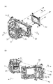
次に、カメラ100の内部の構成について図3を参照して説明する。図3は、カメラの内部の構成を示す斜視図である。図3(a)は、カメラを前面側から見た斜視図であり、図3(b)は、カメラを背面側から見た斜視図である。図3(a)は、構成部品が前面側から撮影光軸に沿って、マウント部2、ミラーボックス20、本体ベース30、撮像ユニット40の順番に配置されている。
Next, the internal configuration of the
カメラ本体1は、本体ベース30を備えている。本体ベース30の被写体側には、上述したミラーボックス20およびシャッタユニット(不図示)がビス等によって取り付けられている。
The camera body 1 includes a
本体ベース30の撮影者側には、後述する撮像ユニット40が配設されている。
An
さらに、撮像ユニット40の周辺の構成について説明する。図3に示すように、カメラ本体の骨格となる本体ベース30の被写体側には、被写体側から順に、ミラーボックス20、シャッタユニット(不図示)が配設される。また、本体ベース30の撮影者側には、撮像ユニット40が配設される。撮像ユニット40は、撮影レンズユニットが取り付けられる基準となるマウント部2の取付面に撮像素子8の撮像面が所定の距離を空けてかつ平行になるように調整されて固定される。
Further, the configuration around the
続いて、図4で撮像ユニット40の構成について詳細に説明する。図4(a)は、撮像ユニット40を前面側から見た斜視図であり、図3(b)は、撮像ユニット40を背面側から見た斜視図である。
Next, the configuration of the
光学ローパスフィルタ410は、水晶からなる1枚の複屈折板であり、その形状は矩形状である。光学ローパスフィルタ410は、撮影有効領域410aの一側方に圧電素子430を配置する周縁部410bを有しており、撮影光軸に対して直交する方向(カメラRL方向)にて非対称である。このようにした光学ローパスフィルタ410の表面には、光学的なコーティングが施されている。
The optical low-
圧電素子430は、単板の矩形の短冊形状を呈し、光学ローパスフィルタ410の周縁部410bにおいて、圧電素子430の長辺が光学ローパスフィルタ410の短辺(側辺)に平行になるように配置されて接着保持される(貼着される)。この圧電素子430は光学ローパスフィルタ410を振動させる振動手段である。すなわち、圧電素子430は、光学ローパスフィルタ410上において四辺のうち一辺に近接して平行に貼着され、一辺に平行な複数の節部を有するように光学ローパスフィルタ410を波状に振動させる。この圧電素子430の駆動により、光学ローパスフィルタ410の表面に付着した塵埃等の異物を除去する機能を備えている。
The
光学ローパスフィルタ保持部材420は光学ローパスフィルタ410を保持する。光学ローパスフィルタ保持部材420は樹脂材料または金属材料で形成され、両面テープ520で撮像素子8に接着固定される。両面テープ520は、撮像素子8に撮影光路外からの余計な光が入射することを防ぐためのマスクの役割を兼ね備えている。
The optical low-pass
圧電素子用フレキシブルプリント基板470は、圧電素子430に接着固定されるとともに、圧電素子430に電圧を印加することができる。圧電素子430は、電圧の印加により光軸と直交する方向(R−L)に主として伸縮振動し、光学ローパスフィルタ410を共振(振動)させる。
The piezoelectric element flexible printed
付勢部材440は、光学ローパスフィルタ410を光軸方向に付勢し、光学ローパスフィルタ保持部材420または撮像素子固定部材510に係止される。付勢部材440は導電性を有する材料で形成されるとともに、ビスにより撮像素子固定部材510に電気的に接続されている。したがって、撮像素子固定部材510は、付勢部材440と接する光学ローパスフィルタ410の表面(光学的なコーティングが施された面)とも電気的に接続される。撮像素子固定部材510はカメラ本体1の接地電位となっている。これにより、光学ローパスフィルタ410の表面も接地電位となり、光学ローパスフィルタ410の表面への塵埃等の静電気的な付着を抑制することができる。
The biasing
光学ローパスフィルタ保持部材420は断面略円形の枠状の弾性部材が二色成型、インサート成型または別体で配置されており、光学ローパスフィルタ410により密着封止される。
The optical low-pass
光学部材460は位相板(偏光解消板)と赤外カットフィルタと光学ローパスフィルタ410に対して屈折方向が90°異なる複屈折板とを貼り合わせている。光学部材460は、光学ローパスフィルタ保持部材420に接着固定される。
The
撮像素子固定部材510は板状に形成され、厚み方向に矩形の開口部700を有している。撮像素子8を撮像素子固定部材510に位置決めした後、撮像素子固定部材510の開口部700に接着剤800を流し込むことで、撮像素子固定部材510と撮像素子8とを接着固定している。撮像素子固定部材510の周囲には、ミラーボックス20にビス固定するための腕部が設けられている。
The imaging
信号処理基板600は、撮像素子8と電気的に接続され、撮像素子8を動作させる回路が実装されている。
The
次に、撮像素子8と撮像素子固定部材510の接着固定について、詳細に説明する。
Next, the adhesion fixing between the
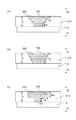
図5は、撮像素子8と撮像素子固定部材510の開口部700を背面から見た図ある。また、図6は、図5のA−A断面図と詳細図である。
FIG. 5 is a view of the
図5に示すように、撮像素子固定部材510には、2つの開口部700が形成されている。開口部700は、撮像素子8の長辺方向における略中央部分に対応する位置にて、撮像素子8の短辺方向に延出して形成される。この開口部700に接着剤800を流し込むことにより、撮像素子8と撮像素子固定部材510は強固に接着固定される。なお、本実施形態では、開口部700を2つ形成する例を説明するが、開口部700は1つであっても、複数形成されていてもよい。
As shown in FIG. 5, two
また、図6の断面図に示すように、開口部700は撮像素子8の裏面と対向しない側に面取り加工を施すことで、面取り部Saが形成されている。すなわち、開口部700は、撮像素子8の裏面と対向しない側に面取り加工を施すことで、撮像素子8の裏面に対向しない側の開口幅が撮像素子8の裏面に対向する側の開口幅よりも大きくなるように形成される。
In addition, as shown in the cross-sectional view of FIG. 6, the chamfered portion Sa is formed by chamfering the
ここで、開口部700の断面について、図7の模式図で詳細に説明する。図7(a)は、本実施形態における開口部700の断面図、図7(b)は、第1の変形例、図7(c)は第2の変形例で、接着剤800を流し込んだ状態または硬化した状態を示している。(a)に示すように、撮像素子固定部材510の厚みをt、開口部700のRr方向側の面取り部をSa、開口部700の光軸に対して平行な面をSbとしている。接着剤800は、撮像素子固定部材510の厚みt内におさまるようにRr側から流し込まれる。接着剤硬化時には、接着界面の範囲がSa+Sb>tとなり、接着界面が長くなるので、厚み方向に垂直な面のみの開口部に比べて接着強度が高くなる。また、Sa面は、Fr方向に撮像素子固定部材510、撮像素子8が配置されており、接着剤800がアンカー構造になっているため、Rr方向の引き剥がし力に対して、接着強度が高くなる。
Here, the cross section of the
図7(b)は、本実施形態の第1の変形例を説明する開口部700の断面図である。Taで示される開口面が光軸に対して全面傾斜しており、図7(a)よりもアンカー効果が強く接着強度が高い。また、接着界面の範囲もTa>tとなる。
FIG. 7B is a cross-sectional view of the
図7(c)は、本実施形態の第2の変形例を説明する開口部700の断面図である。この開口720は、撮像素子に対向しない側に座ぐり加工を施すことで、撮像素子8に対向しない側の開口幅が撮像素子8に対向する側の開口幅よりも大きくなるように形成される。
FIG. 7C is a cross-sectional view of the
図7(c)に図示するように、開口720では、Ua面が撮像素子固定部材510の表面と略平行になっており、アンカー効果が最も高い。また、接着界面の範囲もUa+Ub1+Ub2>tとなり、接着強度は極めて高くなる。
As shown in FIG. 7C, in the opening 720, the Ua surface is substantially parallel to the surface of the image
ただし、図7(b)および(c)は、撮像素子固定部材510が金属部材であると、プレス加工では潰し部が多いため、作成が困難となる。切削加工であれば、形状作成は可能であるが、部品コストが高くなる。したがって、プレス加工のみで作成できる図7(a)のような形状が量産工程では実現しやすい。
However, in FIG. 7B and FIG. 7C, if the imaging
続いて、図5において、撮像素子8に対する開口部700の投影配置に関して詳細に説明する。開口部700の位置は、撮像素子8の裏面に対して、略中央部分に配置することが望ましい。本実施形態では、撮像素子8の裏面の長辺方向(RL方向)で略3等分した領域の中央部分のみに限定して配置している。撮像素子固定部材510は、通常、金属部材であるアルミ、ステンレス、鉄など、またはモールド部品で形成される。これに対して、撮像素子8は、シリコンウエハーから形成されるチップがセラミックなどによりパッケージされる構成である。このため、撮像素子固定部材510と撮像素子8のパッケージの材料が異なると、線膨張係数の差による温度環境下での熱歪み量も異なる。上述したようにデジタル一眼レフカメラでは、撮像素子8のピント方向の位置精度が非常に重要であるため、動作保障されている温度環境下での熱歪みによる撮像素子8の変形などはできる限り低減しておく必要がある。
Next, with reference to FIG. 5, the projection arrangement of the
図8に、撮像素子8と撮像素子固定部材510の線膨張係数の差による熱歪みの影響を示す模式図を示す。図6の断面図で撮像素子8と撮像素子固定部材510、開口部700に特化した模式図である。図8(a)は、本実施形態のように撮像素子8の裏面の略中央部分に開口部700が配置されており、図8(b)は、撮像素子8の裏面の広範囲で略均等に接着用開口部750が配置されている比較例である。
FIG. 8 is a schematic diagram illustrating the influence of thermal strain due to the difference in the linear expansion coefficient between the
この比較例では、撮像素子8に対して、撮像素子固定部材510の線膨張係数が大きい材質で構成されており、雰囲気温度を常温(約23℃)から低温(約−20〜30℃)に推移させた時の状態を示している。例えば、低温下では、撮像素子8、撮像素子固定部材510がそれぞれC1(点線矢印)、C2(実線矢印)の方向に収縮し、その収縮量が異なるために撮像素子8の変形が発生する。このとき、開口部700、つまり接着による連結部が撮像素子8の中央部分に近いほど、変形の影響は少ない(δ1<δ2)。
In this comparative example, the imaging
したがって、開口部700を撮像素子8の略中央に対応する位置に配置させることで、低温、高温での熱歪みによる撮像素子8の変形を低減することが可能である。
Therefore, by disposed at a position corresponding to the
また、本実施形態の開口部700に関して、接着剤800の流し込み作業性についても良好な形状となっている。例えば、使用する接着剤800は、光硬化型のアクリル系、またはエポキシ系の紫外線硬化樹脂であることが望ましい。紫外線硬化樹脂は、速硬化性があり、作業時間を短縮することができる。
In addition, the
図9に撮像ユニット40の背面図を示す。図10は、図9のD−Dにおける断面図と詳細図である。撮像素子8は、撮像素子固定部材510に対して、位置調整した後に開口部700に接着剤800を流し込んで撮像素子固定部材510に接着固定される。その後、信号処理基板600が撮像素子8と半田などにより電気的に接続される。
FIG. 9 shows a rear view of the
図10に示すように、撮像ユニット40の薄型化のため、撮像素子固定部材510と信号処理基板600との隙間は極めて狭くなっている(図中d)。このため、接着剤の流し込み作業において開口部700から接着剤800がはみ出すことは許されない。本実施形態では、開口部700の面取り部Saが形成されているため接着剤800を流し込む側の幅が広いため、接着剤800を流入させやすく、開口部700から接着剤800のはみ出しを防止できる。また、開口部700は撮像素子8の短辺に延出して形成されているため、ディスペンサーなどによる吐出作業も直線動作となり作業効率が良い。さらに、光硬化型接着剤の使用では、接着剤への光照射性が重要であるが、開口部700の照射側の端に面取り部Saが形成されているため、光の照射側の開口幅が広く、接着剤800の厚み方向で照射量が効率よく得られる。
As shown in FIG. 10, the gap between the image
本実施形態の開口部形状での接着固定であれば、撮像ユニット重量の約100倍の接着力を得ることが可能であり、上述したカメラの落下衝撃に対しても十分な精度を保証することが可能である。 If the adhesive fixing in the shape of the opening of the present embodiment, it is possible to obtain an adhesive force about 100 times the weight of the imaging unit, and to ensure sufficient accuracy against the above-described camera drop impact. Is possible.
以上、本発明の好ましい実施形態について説明したが、本発明はこれらの実施形態に限定されず、その要旨の範囲内で種々の変形及び変更が可能である。 As mentioned above, although preferable embodiment of this invention was described, this invention is not limited to these embodiment, A various deformation | transformation and change are possible within the range of the summary.
8 撮像素子
40 撮像ユニット
510 撮像素子固定部材
700 開口部
800 接着剤
8
Claims (6)
前記撮像素子および前記固定部材は、線膨張係数が互いに異なる材料で形成されており、
前記開口部は、前記撮像素子の長辺方向を略3等分した領域の中央部分に対応する領域に複数個形成されており、
前記複数の開口部は、前記撮像素子に対向しない側の開口幅が前記撮像素子に対向する側の開口幅よりも大きくなるように、それぞれ形成されており、
前記複数の開口部には、前記撮像素子の光軸方向に対して傾いた傾斜面がそれぞれ形成されており、
前記傾斜面の少なくとも一部が硬化した前記接着剤で満たされていることを特徴とする撮像装置。 An imaging element; and a fixing member in which an opening is formed, wherein the imaging element is positioned on the fixing member, and adhesive is poured into the opening so that the imaging element is fixed. An imaging device that is adhesively fixed to a member,
The imaging element and the fixing member are formed of materials having different linear expansion coefficients,
A plurality of the openings are formed in a region corresponding to a central portion of a region obtained by dividing the long side direction of the imaging element into approximately three equal parts,
The plurality of openings are each formed such that the opening width on the side not facing the imaging element is larger than the opening width on the side facing the imaging element,
In the plurality of openings, inclined surfaces that are inclined with respect to the optical axis direction of the imaging element are formed, respectively.
At least partially filled with the adhesive cured imaging apparatus characterized by Tei Rukoto before Symbol inclined surface.
前記撮像素子および前記固定部材は、線膨張係数が互いに異なる材料で形成されており、
前記開口部は、前記撮像素子の長辺方向を略3等分した領域の中央部分に対応する位置に複数個形成されており、
前記複数の開口部は、前記撮像素子に対向しない側の開口幅が前記撮像素子に対向する側の開口幅よりも大きくなるように、それぞれ形成されており、
前記複数の開口部には、前記固定部材の表面と略平行な平行面がそれぞれ形成されており、
前記平行面の少なくとも一部が硬化した前記接着剤で満たされていることを特徴とする撮像装置。 An imaging element; and a fixing member in which an opening is formed, wherein the imaging element is positioned on the fixing member, and adhesive is poured into the opening so that the imaging element is fixed. An imaging device that is adhesively fixed to a member,
The imaging element and the fixing member are formed of materials having different linear expansion coefficients,
A plurality of the openings are formed at positions corresponding to a central portion of a region obtained by dividing the long side direction of the imaging element into approximately three equal parts,
The plurality of openings are each formed such that the opening width on the side not facing the imaging element is larger than the opening width on the side facing the imaging element,
The plurality of openings are each formed with a parallel surface substantially parallel to the surface of the fixing member,
At least partially filled with the adhesive cured imaging apparatus characterized by Tei Rukoto before Symbol parallel surfaces.
Priority Applications (3)
| Application Number | Priority Date | Filing Date | Title |
|---|---|---|---|
| JP2011098587A JP5864890B2 (en) | 2011-04-26 | 2011-04-26 | Imaging device |
| CN2012101206197A CN102761686A (en) | 2011-04-26 | 2012-04-23 | Imaging apparatus |
| US13/454,995 US9291881B2 (en) | 2011-04-26 | 2012-04-24 | Imaging apparatus |
Applications Claiming Priority (1)
| Application Number | Priority Date | Filing Date | Title |
|---|---|---|---|
| JP2011098587A JP5864890B2 (en) | 2011-04-26 | 2011-04-26 | Imaging device |
Publications (3)
| Publication Number | Publication Date |
|---|---|
| JP2012230259A JP2012230259A (en) | 2012-11-22 |
| JP2012230259A5 JP2012230259A5 (en) | 2014-06-19 |
| JP5864890B2 true JP5864890B2 (en) | 2016-02-17 |
Family
ID=47056001
Family Applications (1)
| Application Number | Title | Priority Date | Filing Date |
|---|---|---|---|
| JP2011098587A Expired - Fee Related JP5864890B2 (en) | 2011-04-26 | 2011-04-26 | Imaging device |
Country Status (3)
| Country | Link |
|---|---|
| US (1) | US9291881B2 (en) |
| JP (1) | JP5864890B2 (en) |
| CN (1) | CN102761686A (en) |
Families Citing this family (4)
| Publication number | Priority date | Publication date | Assignee | Title |
|---|---|---|---|---|
| JP5864890B2 (en) * | 2011-04-26 | 2016-02-17 | キヤノン株式会社 | Imaging device |
| TWI545424B (en) * | 2013-09-18 | 2016-08-11 | 微太科技股份有限公司 | Camera angle switching device and the method of handling the article |
| JP6524951B2 (en) * | 2016-03-30 | 2019-06-05 | パナソニックIpマネジメント株式会社 | The camera module |
| JP6666044B2 (en) | 2016-04-27 | 2020-03-13 | キヤノン株式会社 | Imaging device |
Family Cites Families (25)
| Publication number | Priority date | Publication date | Assignee | Title |
|---|---|---|---|---|
| US5455386A (en) * | 1994-01-14 | 1995-10-03 | Olin Corporation | Chamfered electronic package component |
| US5837090A (en) * | 1994-12-08 | 1998-11-17 | Raytheon Company | Precision aligning and joining of two articles using a flowable adhesive |
| US6654064B2 (en) * | 1997-05-23 | 2003-11-25 | Canon Kabushiki Kaisha | Image pickup device incorporating a position defining member |
| JP4169938B2 (en) * | 2000-01-28 | 2008-10-22 | Hoya株式会社 | Solid-state image sensor holding block and solid-state image sensor mounting structure |
| US6956615B2 (en) * | 2000-01-28 | 2005-10-18 | Pentax Corporation | Structure for mounting a solid-state imaging device |
| JP4079343B2 (en) * | 2001-06-07 | 2008-04-23 | 株式会社リコー | Image reading apparatus and image forming apparatus |
| JP4477811B2 (en) * | 2002-02-27 | 2010-06-09 | Hoya株式会社 | Mounting plate for solid-state image sensor and mounting method to the mounting plate |
| US7583309B2 (en) * | 2002-06-28 | 2009-09-01 | Kyocera Coproration | Imaging device package camera module and camera module producing method |
| US20040238947A1 (en) * | 2003-05-28 | 2004-12-02 | Intel Corporation | Package and method for attaching an integrated heat spreader |
| JP2006081008A (en) * | 2004-09-10 | 2006-03-23 | Olympus Corp | Optical device |
| JP2006094444A (en) * | 2004-09-27 | 2006-04-06 | Casio Comput Co Ltd | Fixing structure of solid-state imaging device |
| JP4471853B2 (en) | 2005-01-21 | 2010-06-02 | Hoya株式会社 | Digital camera |
| US7829833B2 (en) * | 2005-05-24 | 2010-11-09 | Olympus Imaging Corp. | Arranging and/or supporting an image pickup device in an image pickup apparatus |
| JP4555732B2 (en) * | 2005-05-24 | 2010-10-06 | オリンパスイメージング株式会社 | Imaging device |
| JP4818750B2 (en) * | 2006-02-23 | 2011-11-16 | オリンパスイメージング株式会社 | Imaging device |
| JP4668036B2 (en) * | 2005-11-02 | 2011-04-13 | Hoya株式会社 | Mounting structure for FPC of image sensor |
| US7399930B1 (en) * | 2007-01-16 | 2008-07-15 | International Business Machines Corporation | Method and device for repair of a contact pad of a printed circuit board |
| JP4280779B2 (en) * | 2007-01-31 | 2009-06-17 | キヤノン株式会社 | Imaging device |
| CN100576555C (en) * | 2007-08-09 | 2009-12-30 | 佛山普立华科技有限公司 | Device for image |
| TW200951616A (en) * | 2008-06-05 | 2009-12-16 | Asia Optical Co Inc | Image sensing module |
| CN201289538Y (en) * | 2008-03-31 | 2009-08-12 | 富士能株式会社 | Lens assembling body and photographic device |
| JP4560121B2 (en) * | 2008-12-17 | 2010-10-13 | 株式会社東芝 | Sensor fixing device and camera module |
| US8553131B2 (en) * | 2010-06-03 | 2013-10-08 | Bendix Commercial Vehicle Systems Llc | Six-axis mount |
| JP5093324B2 (en) * | 2010-10-08 | 2012-12-12 | カシオ計算機株式会社 | Solid-state image pickup device unit, manufacturing method thereof, and image pickup apparatus |
| JP5864890B2 (en) * | 2011-04-26 | 2016-02-17 | キヤノン株式会社 | Imaging device |
-
2011
- 2011-04-26 JP JP2011098587A patent/JP5864890B2/en not_active Expired - Fee Related
-
2012
- 2012-04-23 CN CN2012101206197A patent/CN102761686A/en active Pending
- 2012-04-24 US US13/454,995 patent/US9291881B2/en not_active Expired - Fee Related
Also Published As
| Publication number | Publication date |
|---|---|
| US20120273656A1 (en) | 2012-11-01 |
| JP2012230259A (en) | 2012-11-22 |
| US9291881B2 (en) | 2016-03-22 |
| CN102761686A (en) | 2012-10-31 |
Similar Documents
| Publication | Publication Date | Title |
|---|---|---|
| JP5864890B2 (en) | Imaging device | |
| JP5169504B2 (en) | Optical components and optical equipment | |
| JP4818750B2 (en) | Imaging device | |
| JP6639290B2 (en) | Imaging device | |
| JP3989295B2 (en) | Camera and image sensor unit used therefor | |
| JP4300617B2 (en) | Optical device | |
| JP4119703B2 (en) | Camera and image sensor unit used therefor | |
| JP4017908B2 (en) | camera | |
| JP3989293B2 (en) | Camera and image sensor unit used therefor | |
| JP5262135B2 (en) | Optical components and optical equipment | |
| JP2015015529A (en) | Imaging unit and imaging apparatus | |
| JP2004187243A (en) | Image pickup device | |
| JP2017199989A (en) | Imaging apparatus | |
| JP3989296B2 (en) | Camera and image sensor unit | |
| JP5332622B2 (en) | Imaging device | |
| JP2021087032A (en) | Module, electronic viewfinder, and imaging device | |
| JP5233586B2 (en) | Imaging apparatus, optical apparatus, and manufacturing method of imaging apparatus | |
| JP6746466B2 (en) | Electronics | |
| US20230421875A1 (en) | Imaging apparatus | |
| JP2009130615A (en) | Imaging device and optical apparatus | |
| JP5734119B2 (en) | Imaging device | |
| JP5228507B2 (en) | Optical component, imaging device and optical apparatus | |
| JP2003348397A (en) | Camera and imaging device unit to be used therefor | |
| JP3989294B2 (en) | Camera and image sensor unit used therefor | |
| JP2017169176A (en) | Imaging apparatus |
Legal Events
| Date | Code | Title | Description |
|---|---|---|---|
| A521 | Request for written amendment filed |
Free format text: JAPANESE INTERMEDIATE CODE: A523 Effective date: 20140428 |
|
| A621 | Written request for application examination |
Free format text: JAPANESE INTERMEDIATE CODE: A621 Effective date: 20140428 |
|
| A131 | Notification of reasons for refusal |
Free format text: JAPANESE INTERMEDIATE CODE: A131 Effective date: 20150120 |
|
| A977 | Report on retrieval |
Free format text: JAPANESE INTERMEDIATE CODE: A971007 Effective date: 20150121 |
|
| A521 | Request for written amendment filed |
Free format text: JAPANESE INTERMEDIATE CODE: A523 Effective date: 20150323 |
|
| A131 | Notification of reasons for refusal |
Free format text: JAPANESE INTERMEDIATE CODE: A131 Effective date: 20150728 |
|
| A521 | Request for written amendment filed |
Free format text: JAPANESE INTERMEDIATE CODE: A523 Effective date: 20150917 |
|
| A131 | Notification of reasons for refusal |
Free format text: JAPANESE INTERMEDIATE CODE: A131 Effective date: 20151020 |
|
| A521 | Request for written amendment filed |
Free format text: JAPANESE INTERMEDIATE CODE: A523 Effective date: 20151106 |
|
| TRDD | Decision of grant or rejection written | ||
| A01 | Written decision to grant a patent or to grant a registration (utility model) |
Free format text: JAPANESE INTERMEDIATE CODE: A01 Effective date: 20151201 |
|
| A61 | First payment of annual fees (during grant procedure) |
Free format text: JAPANESE INTERMEDIATE CODE: A61 Effective date: 20151225 |
|
| R151 | Written notification of patent or utility model registration |
Ref document number: 5864890 Country of ref document: JP Free format text: JAPANESE INTERMEDIATE CODE: R151 |
|
| LAPS | Cancellation because of no payment of annual fees |