JP5864468B2 - Dielectric waveguide input / output structure - Google Patents
Dielectric waveguide input / output structure Download PDFInfo
- Publication number
- JP5864468B2 JP5864468B2 JP2013071502A JP2013071502A JP5864468B2 JP 5864468 B2 JP5864468 B2 JP 5864468B2 JP 2013071502 A JP2013071502 A JP 2013071502A JP 2013071502 A JP2013071502 A JP 2013071502A JP 5864468 B2 JP5864468 B2 JP 5864468B2
- Authority
- JP
- Japan
- Prior art keywords
- dielectric
- dielectric waveguide
- output structure
- waveguide
- input
- Prior art date
- Legal status (The legal status is an assumption and is not a legal conclusion. Google has not performed a legal analysis and makes no representation as to the accuracy of the status listed.)
- Expired - Fee Related
Links
Images


Classifications
-
- H—ELECTRICITY
- H01—ELECTRIC ELEMENTS
- H01P—WAVEGUIDES; RESONATORS, LINES, OR OTHER DEVICES OF THE WAVEGUIDE TYPE
- H01P5/00—Coupling devices of the waveguide type
- H01P5/08—Coupling devices of the waveguide type for linking dissimilar lines or devices
- H01P5/10—Coupling devices of the waveguide type for linking dissimilar lines or devices for coupling balanced with unbalanced lines or devices
- H01P5/1022—Transitions to dielectric waveguide
-
- H—ELECTRICITY
- H01—ELECTRIC ELEMENTS
- H01P—WAVEGUIDES; RESONATORS, LINES, OR OTHER DEVICES OF THE WAVEGUIDE TYPE
- H01P3/00—Waveguides; Transmission lines of the waveguide type
- H01P3/16—Dielectric waveguides, i.e. without a longitudinal conductor
-
- H—ELECTRICITY
- H01—ELECTRIC ELEMENTS
- H01P—WAVEGUIDES; RESONATORS, LINES, OR OTHER DEVICES OF THE WAVEGUIDE TYPE
- H01P1/00—Auxiliary devices
- H01P1/20—Frequency-selective devices, e.g. filters
- H01P1/2002—Dielectric waveguide filters
-
- H—ELECTRICITY
- H01—ELECTRIC ELEMENTS
- H01P—WAVEGUIDES; RESONATORS, LINES, OR OTHER DEVICES OF THE WAVEGUIDE TYPE
- H01P5/00—Coupling devices of the waveguide type
- H01P5/08—Coupling devices of the waveguide type for linking dissimilar lines or devices
- H01P5/087—Transitions to a dielectric waveguide
Landscapes
- Control Of Motors That Do Not Use Commutators (AREA)
- Waveguides (AREA)
Description
本発明は、誘電体導波管の入出力構造に関し、特に誘電体導波管と同軸線路との変換構造に関する。 The present invention relates to an input / output structure of a dielectric waveguide, and more particularly to a conversion structure between a dielectric waveguide and a coaxial line.
誘電体材料の表面に導体膜を形成して得られる誘電体導波管は、肉厚の導体壁が不要であることと、誘電体材料による電磁波の短縮効果とにより、古くから用いられてきた空洞導波管と比較して導波管装置を大幅に小型化することができる。このような導波管装置は、基板に直接実装できる程に小型であることから、誘電体導波管をマイクロストリップ線路が設けられた実装基板に半田付けして入出力を行なう、誘電体導波管−マイクロストリップ変換構造を用いた入出力構造が利用されてきた(例えば、特許文献1参照)。 Dielectric waveguides obtained by forming a conductor film on the surface of a dielectric material have been used for a long time due to the fact that a thick conductor wall is unnecessary and the effect of shortening electromagnetic waves by the dielectric material. Compared with the hollow waveguide, the waveguide device can be significantly reduced in size. Since such a waveguide device is small enough to be directly mounted on a substrate, a dielectric waveguide is used for input / output by soldering the dielectric waveguide to a mounting substrate provided with a microstrip line. An input / output structure using a wave tube-microstrip conversion structure has been used (see, for example, Patent Document 1).
図9は、従来の誘電体導波管入出力構造である誘電体導波管−マイクロストリップ変換構造を用いた誘電体導波管フィルタの分解透視斜視図を示す。図9に示すように、誘電体導波管フィルタ1は、外周を導体膜で覆われた直方体形状の誘電体ブロックからなる誘電体導波管1a、1b、1c、1d、1eが一連に接続され、
誘電体導波管1aと1bとの間には誘電体が露出する結合窓4aと、
誘電体導波管1bと1cとの間には誘電体が露出する結合窓4bと、
誘電体導波管1cと1dとの間には誘電体が露出する結合窓4cと、
誘電体導波管1dと1eとの間には誘電体が露出する結合窓4dと、
が設けられている。
両端の誘電体導波管1a、1eのそれぞれの下面には、導体膜と電気的に絶縁された島状電極5a、5eが設けられている。
FIG. 9 is an exploded perspective view of a dielectric waveguide filter using a dielectric waveguide-microstrip conversion structure, which is a conventional dielectric waveguide input / output structure. As shown in FIG. 9, the
Between the dielectric waveguides 1a and 1b, a coupling window 4a through which the dielectric is exposed,
Between the dielectric waveguides 1b and 1c, a
Between the dielectric waveguides 1c and 1d, a coupling window 4c through which the dielectric is exposed,
Between the dielectric waveguides 1d and 1e, a
Is provided.
On the lower surfaces of the dielectric waveguides 1a and 1e at both ends, island-
プリント基板8は、表面に島状電極8bと、裏面にマイクロストリップ8aと、島状電極8bとマイクロストリップ8aとを接続するスルーホール8cとが設けられている。
誘電体導波管1a、1eは、誘電体導波管1a、1eの底面に設けられた島状電極5a、5eと、プリント基板8、8の表面に設けられた島状電極8b、8bとがそれぞれ対向するように配置される。
The printed circuit board 8 is provided with an
The dielectric waveguides 1a and 1e include island-
誘電体導波管を同軸線路に接続したい場合に、誘電体導波管の内部に誘電体が充填されているため、導波管内部に構造物を挿入することができないので、空洞導波管で用いられてきたプローブを空洞導波管内部に挿入する、空洞導波管−同軸線路変換構造を用いることが困難である。そのため、図8に示すように、一度、損失の大きいマイクロストリップ線路8aに変換してから、さらに、マイクロストリップ−同軸変換を用いて、コネクタ7に変換する、誘電体誘電体導波管−マイクロストリップ−同軸変換を用いる必要があり、性能の劣化が避けられないという問題があった。また、マイクロストリップ8aは、ある程度以上の長さが必要なため、プリント基板8を小さくすることができず、入出力構造の小型化の阻害要因となっていた。
When it is desired to connect the dielectric waveguide to the coaxial line, the dielectric waveguide is filled with a dielectric, so that a structure cannot be inserted into the waveguide. It is difficult to use a cavity waveguide-coaxial line conversion structure in which the probe used in the above is inserted into the cavity waveguide. Therefore, as shown in FIG. 8, once converted into a
本発明の誘電体導波管入出力構造は、
外周を導体膜で覆われた直方体形状の誘電体の側面にコネクタと他の誘電体導波管と接続するための誘電体が露出する結合窓とを有する誘電体導波管において、
前記誘電体導波管は、
直方体形状の誘電体ブロックと、板状の誘電体板とを厚み方向に積み重ねて、線状の導体箔からなる給電線を挟んだ
ことを特徴とする。
The dielectric waveguide input / output structure of the present invention is
In a dielectric waveguide having a coupling window through which a dielectric for connecting to a connector and another dielectric waveguide is exposed on a side surface of a rectangular parallelepiped dielectric whose outer periphery is covered with a conductor film,
The dielectric waveguide is
It is characterized in that a rectangular parallelepiped dielectric block and a plate-like dielectric plate are stacked in the thickness direction, and a feeder line made of a linear conductor foil is sandwiched therebetween.
本発明の誘電体導波管入出力構造によれば、マイクロストリップに変換することなく、誘電体導波管と同軸線路とを直接変換することができるので、性能の劣化が少ない入出力構造とすることができ、また、マイクロストリップ線路のためのプリント基板が不要なので、入出力構造を小型化することができる。 According to the dielectric waveguide input / output structure of the present invention, since the dielectric waveguide and the coaxial line can be directly converted without being converted into the microstrip, the input / output structure with little deterioration in performance In addition, since the printed circuit board for the microstrip line is unnecessary, the input / output structure can be reduced in size.
(実施例1)
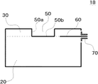
以下、図面を用いて本発明の第1の実施例を説明する。図1は、本発明の誘電体導波管入出力構造を有する誘電体導波管の第1の実施例を詳細に説明するための分解斜視図を示し、図2は、図1のA−A断面図を示す。図1において斜線部は誘電体露出部を示している。
図に示すように誘電体導波管18は、直方体形状の誘電体ブロック20と、略中央に直径φの円形の貫通孔50が設けられた板状の誘電体板30とで、線状の導体箔からなる給電線60を挟んでいる。誘電体導波管18は、貫通孔50の内側の側面50aおよび底面50bとを含む外周を導体膜で被覆されている。給電線60の端部は、誘電体導波管18の側面に設けられた導体膜とは絶縁された島状電極90に接続されている。すなわち、誘電体導波管18は横方向からの給電されている。
誘電体導波管18は、島状電極90に接続されたコネクタ70を介して図示しない外部装置と接続されるとともに、誘電体導波管18の側面に設けられた誘電体が露出する結合窓40を介して別の誘電体導波管と接続される。
Example 1
Hereinafter, a first embodiment of the present invention will be described with reference to the drawings. FIG. 1 is an exploded perspective view for explaining in detail a first embodiment of a dielectric waveguide having a dielectric waveguide input / output structure of the present invention, and FIG. A sectional view is shown. In FIG. 1, the shaded portion indicates the dielectric exposed portion.
As shown in the figure, the
The
誘電体ブロック20と誘電体板30とは接合ガラスを用いて接着され、外装の導体膜、島状電極90および給電線60は、銀ペーストを印刷後に焼結して形成されている。
The
上記した誘電体導波管18は、直接、誘電体導波管を同軸線路に変換することができるので性能の劣化が少なく、マイクロストリップ線路のためのプリント基板が必要ないので、誘電体導波管入出力構造を小型化することができる。
Since the
なお、このような共振器内に凸部を設ける構造は、リエントラント構造と呼ばれ、誘電体導波管の管軸方向の長さを短縮して誘電体導波管の専有面積を小さくすることと、抑制することの難しい3倍高調波を抑制することができること、とが知られているが、貫通孔50がない誘電体導波管18は、横方向からの給電では上手く発振することができない。したがって、貫通孔50を設けることにより、誘電体導波管18を上手く動作させるとともに、導波管長を短縮し、3倍高調波を抑制することができる。また、誘電体導波管18は変換部が外部に露出せず誘電体内にあるので、不要な放射を減らす効果もある。
Such a structure in which a convex portion is provided in the resonator is called a reentrant structure, and the length of the dielectric waveguide in the tube axis direction is shortened to reduce the area occupied by the dielectric waveguide. It is known that the third harmonic that is difficult to suppress can be suppressed, but the
リエントラント構造では、貫通孔50の底面部50aは誘電体が露出していても特性への影響は少ないため、貫通孔50の底面部50aには導体膜がなくてもよい。
また、誘電体ブロック20はTEモードに近いモードで動作し、誘電体板30はTEMモードに近いモードで動作していると考えられ、誘電体ブロック20と誘電体板30とでは動作モードが異なっていると考えられる。したがって、誘電体ブロック20と誘電体板30との間の境界が特性へ与える影響は小さく、誘電体ブロック20と誘電体板30との間に接合ガラスによるギャップがあっても特性への影響は少ない。接合ガラスは、誘電体ブロック20および誘電体板30に近い比誘電率の接合ガラスが好適である。
In the reentrant structure, the
In addition, it is considered that the
また、誘電体ブロック20と誘電体板30との比誘電率を変えても構わない。非誘電率の高い誘電体材料は高価なので、例えば、誘電体板30には誘電体ブロック20より比誘電率の低く安価な誘電体材料とすることにより、誘電体導波管入出力構造の価格を抑えることもできる。
Further, the relative dielectric constant between the
(実施例2)
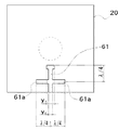
図3は、本発明の誘電体導波管入出力構造を有する誘電体導波管の第2の実施例を詳細に説明するための分解斜視図を示し、図4は、図3の給電線を詳しく説明するための誘電体ブロックの平面図を示す。図3乃至図4において、図1乃至図2で説明したものと同一部分には同じ番号を付して重複する説明を省略する。第2の実施例に係る誘電体導波管19は、第1の実施例に示した誘電体導波管とほぼ同様であるが、給電線60の形状が異なる。
(Example 2)
FIG. 3 is an exploded perspective view for explaining in detail the second embodiment of the dielectric waveguide having the dielectric waveguide input / output structure of the present invention, and FIG. 4 shows the feeder line of FIG. The top view of the dielectric material block for explaining this in detail is shown. 3 to 4, the same parts as those described with reference to FIGS. 1 and 2 are denoted by the same reference numerals, and redundant description is omitted. The
図3に示すように、給電線61の先端の幅y1は、根本部の幅y0より太くなっており(y1>y0)、給電線61の先端と貫通孔50との間の距離はd離れている。また、先端から略四分の一波長離れた両側面には、略四分の一波長の長さのオープンスタブ61aが設けられている。
As shown in FIG. 3, the width y 1 of the front end of the
オープンスタブ61aを設けることにより、2倍高調波を抑制することができ、給電線61の先端部の幅y1を、根本部の幅y0より広くしたことにより、先端を貫通孔から距離を離して耐電力特性を高めるとともに、外部Qを低く抑えて入出力構造を広帯域化することができる。
By providing an
上記した誘電体導波管19は、第1の実施例で示した誘電体導波管の給電線の形状を変えるだけで、2倍高調波を抑制するとともに耐電力特性を高め、広帯域化した入出力構造とすることができる。
The
(実施例3)
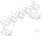
図5は、第2の実施例に示した誘電体導波管を誘電体導波管フィルタに適用した分解透視斜視図を示す。図5に示すように、誘電体導波管フィルタ100は、外周を導体膜で被覆された長方体形の誘電体導波管11〜15が一連に接続され、
誘電体導波管11と12との間には誘電体が露出する結合窓w41と、
誘電体導波管12と13との間には誘電体が露出する結合窓w42と、
誘電体導波管13と14との間には誘電体が露出する結合窓w43と、
誘電体導波管14と15との間には誘電体が露出する結合窓w44と、
が設けられている。
(Example 3)
FIG. 5 shows an exploded perspective view in which the dielectric waveguide shown in the second embodiment is applied to a dielectric waveguide filter. As shown in FIG. 5, the
Between the
Between the
Between the
Between the
Is provided.
両端の誘電体導波管11、15は、直方体形状の誘電体ブロック20と、略中央に直径φの円形の貫通孔50が設けられた板状の誘電体板30とで、線状の導体箔からなる給電線60を挟んでいる。給電線60の端部は、誘電体導波管18の側面に設けられた導体膜とは絶縁された島状電極90に接続されている。
誘電体導波管11、15は、島状電極90に接続されたコネクタ70を介して図示しない外部装置と接続される。
給電線61の先端の幅は、根本部の幅より太くなっており、先端から略四分の一波長離れた両側面には、略四分の一波長の長さのオープンスタブ61aが設けられている。
The
The
The width of the tip of the
上記した誘電体導波管フィルタ100は、直接、誘電体導波管を同軸線路に変換することができる誘電体導波管入出力構造を用いているので、入出力構造での性能の劣化が少なく、また、マイクロストリップ線路のためのプリント基板が必要がないので誘電体導波管フィルタを小型化することができる。
Since the
図6〜8に、図5に示した本発明の第3の実施例である誘電体導波管フィルタ100と、図7に示した従来の誘電体導波管フィルタ1との特性を比較するグラフを示す。
図4は、通過帯域付近の反射損失(S11)と挿入損失(S21)とのグラフであり、図5は、通過帯域の2倍付近の挿入損失(S21)のグラフであり、図6は、通過帯域の3倍付近の挿入損失(S21)のグラフである。
それぞれの図において、横軸は周波数f[GHz]、縦軸は[dB]を示し、誘電体導波管フィルタ100の特性を実線で示し、誘電体導波管フィルタ1の特性を点線で示す。
6 to 8 compare the characteristics of the
4 is a graph of reflection loss (S11) and insertion loss (S21) in the vicinity of the pass band, FIG. 5 is a graph of insertion loss (S21) in the vicinity of twice the pass band, and FIG. It is a graph of insertion loss (S21) near 3 times the pass band.
In each figure, the horizontal axis indicates the frequency f [GHz], the vertical axis indicates [dB], the characteristic of the
なお、それぞれの誘電体導波管フィルタ1、100は、通過帯域の中心周波数f0=2.12[GHz]、帯域幅fw=40[MHz]として設計されている。
誘電体導波管フィルタ100において、
誘電体ブロック20は、a20×b20×L20=24.0mm×8.0mm×15.00mm、
誘電体板30は、 a30×b30×L30=24.0mm×4.1mm×15.00mm、
誘電体導波管12は、a22×b22×L22=24.0mm×8.0mm×20.14mm、
誘電体導波管13は、a23×b23×L23=24.0mm×8.0mm×20.39mm、
誘電体導波管14は、a24×b24×L24=24.0mm×8.0mm×20.14mm、
結合窓41は、w41×h41=6.59mm×3.0mm、
結合窓42は、w42×h42=5.11mm×3.0mm、
結合窓43は、w43×h43=5.11mm×3.0mm、
結合窓44は、w44×h44=6.59mm×3.0mm、
給電線60の先端部の幅y1は、1.6mm、根本部の幅y0は、0.5mm、
貫通孔50は、φ=3.8mm、
貫通孔50と給電線60との距離dは、1.73mm、
であり、
誘電体導波管フィルタ1において、
誘電体導波管1aは、a1×b1×L1=24.0mm×8.0mm×22.86mm、
誘電体導波管1bは、a2×b2×L2=24.0mm×8.0mm×19.78mm、
誘電体導波管1cは、a3×b3×L3=24.0mm×8.0mm×19.91mm、
誘電体導波管1dは、a4×b4×L4=24.0mm×8.0mm×19.78mm、
誘電体導波管1eは、a5×b5×L5=24.0mm×8.0mm×22.86mm、
結合窓4aは、w1×h1=6.59mm×3.0mm、
結合窓4bは、w2×h2=5.11mm×3.0mm、
結合窓4cは、w3×h3=5.11mm×3.0mm、
結合窓4dは、w4×h4=6.59mm×3.0mm、
である。
なお、誘電体ブロック、誘電体板の比誘電率εは、全て、20.0である。
Each of the
In the
The
The
The
The
The
The
The
The
The
The width y 1 of the front end portion of the
The through
The distance d between the through
And
In the
The dielectric waveguide 1a has a 1 × b 1 × L 1 = 24.0 mm × 8.0 mm × 22.86 mm,
The dielectric waveguide 1b has a 2 × b 2 × L 2 = 24.0 mm × 8.0 mm × 19.78 mm,
The dielectric waveguide 1c has a 3 × b 3 × L 3 = 24.0 mm × 8.0 mm × 19.91 mm,
The dielectric waveguide 1d has a 4 × b 4 × L 4 = 24.0 mm × 8.0 mm × 19.78 mm,
Dielectric waveguide 1e has a 5 × b 5 × L 5 = 24.0 mm × 8.0 mm × 22.86 mm,
The coupling window 4a has w 1 × h 1 = 6.59 mm × 3.0 mm,
The
The coupling window 4c has w 3 × h 3 = 5.11 mm × 3.0 mm,
The
It is.
The relative permittivity ε of the dielectric block and the dielectric plate is all 20.0.
図6の結果から、通過帯域付近の挿入損失(S11)および反射損失(S21)は、本発明の誘電体導波管フィルタ100と従来の誘電体導波管フィルタ1とは略同等であることがわかる。
また、図7の結果から、通過帯域の2倍付近の反射損失(S21)は、従来の誘電体導波管フィルタ1より、本発明の誘電体導波管フィルタ100が、小さくなっていることがわかる。
さらに、図8の結果から、通過帯域の3倍付近の反射損失(S21)は、従来の誘電体導波管フィルタ1より、本発明の誘電体導波管フィルタの100が、小さくなっていることがわかる。
From the results of FIG. 6, the insertion loss (S11) and the reflection loss (S21) near the passband are substantially the same as those of the
Further, from the result of FIG. 7, the
Further, from the result of FIG. 8, the reflection loss (S21) in the vicinity of three times the pass band is smaller in the
このように、本発明の誘電体導波管フィルタ100は、マイクロストリップに変換することなく、誘電体導波管と同軸線路とを直接変換することができるので、性能劣化が少ないとすることができるとともに、マイクロストリップ線路のためのプリント基板を省略でき、また、リエントラント構造とすることにより管軸長を短くできるので、誘電体導波管入出力構造を小型化することができる。
As described above, the
また、本発明の誘電体導波管フィルタ100は、オープンスタブを設けることにより2倍高調波を抑制し、リエントラント構造とすることにより、抑制することの難しい3倍高調波をも抑制することができる。その結果、高調波の少ない誘電体導波管フィルタとすることができる。その結果、高調波を抑制するためのローパスフィルタを別途必要としない。
さらにまた、給電線と装荷されたオープンスタブが導波管内部に配置されて、外部に露出していないので、入出力変換部における不要な放射も抑制することができる。
In addition, the
Furthermore, since the open stub loaded with the feeder line is disposed inside the waveguide and is not exposed to the outside, unnecessary radiation in the input / output conversion unit can be suppressed.
給電線は、誘電体導波管の連結方向とは直交する方向に引き出されているが、いずれの方向でも構わない。誘電体ブロックの長手方向に引き出せば、短手方向よりから引き出すよりも寸法の制限が少なくなり、例えば、給電線の先端と貫通孔との間の距離を大きくすることができるので、耐電力特性を高められる。 The feed line is drawn out in a direction orthogonal to the connecting direction of the dielectric waveguides, but may be in any direction. If the dielectric block is pulled out in the longitudinal direction, the size is less restricted than that from the short side direction. For example, the distance between the tip of the feeder line and the through hole can be increased. Can be enhanced.
なお、本発明の誘電体導波管入出力構造は、誘電体導波管フィルタの入出力構造に限るものではなく、外部装置との接続を有する種々の誘電体導波管装置に適用可能である。 The dielectric waveguide input / output structure of the present invention is not limited to the input / output structure of the dielectric waveguide filter, and can be applied to various dielectric waveguide devices having connections with external devices. is there.
1a〜1e、10〜15、18,19 誘電体導波管
20 誘電体ブロック
30 誘電体板
4a〜4d、40〜44 結合窓
50 貫通孔
60、61 給電線
61a オープンスタブ
7、70 コネクタ
8 プリント基板
8a マイクロストリップ
8cスルーホール
5a、5e、8b、90 島状電極
1、100 誘電体導波管フィルタ
1a to 1e, 10 to 15, 18, 19
Claims (4)
前記誘電体導波管は、直方体形状の誘電体ブロックと、板状の誘電体板とで、線状の導体箔からなる給電線を挟み、
前記誘電体板は、主面略中央に貫通孔を有し、
前記貫通孔の内側の側面は導体膜で被覆されている
ことを特徴とする誘電体導波管入出力構造。 In the input / output structure with a dielectric waveguide whose surface is covered with a conductor film,
The dielectric waveguide has a rectangular parallelepiped-shaped dielectric block and a plate-shaped dielectric plate sandwiching a power supply line made of a linear conductor foil,
The dielectric plate has a through hole in the center of the main surface,
A dielectric waveguide input / output structure characterized in that the inner side surface of the through hole is covered with a conductor film.
請求項1に記載の誘電体導波管入出力構造。 The dielectric waveguide input / output structure according to claim 1, wherein the power supply line is provided with open stubs on both side surfaces.
請求項1に記載の誘電体導波管入出力構造。 2. The dielectric waveguide input / output structure according to claim 1, wherein a width of a tip of the feeder line is wide.
Priority Applications (3)
| Application Number | Priority Date | Filing Date | Title |
|---|---|---|---|
| JP2013071502A JP5864468B2 (en) | 2013-03-29 | 2013-03-29 | Dielectric waveguide input / output structure |
| KR1020140035877A KR20140118891A (en) | 2013-03-29 | 2014-03-27 | Input/output structure for dielectric waveguide |
| US14/229,397 US9437913B2 (en) | 2013-03-29 | 2014-03-28 | Dielectric waveguide comprised of a dielectric block and a dielectric plate sandwiching an input/output feeder line |
Applications Claiming Priority (1)
| Application Number | Priority Date | Filing Date | Title |
|---|---|---|---|
| JP2013071502A JP5864468B2 (en) | 2013-03-29 | 2013-03-29 | Dielectric waveguide input / output structure |
Publications (3)
| Publication Number | Publication Date |
|---|---|
| JP2014197725A JP2014197725A (en) | 2014-10-16 |
| JP2014197725A5 JP2014197725A5 (en) | 2015-01-29 |
| JP5864468B2 true JP5864468B2 (en) | 2016-02-17 |
Family
ID=51620199
Family Applications (1)
| Application Number | Title | Priority Date | Filing Date |
|---|---|---|---|
| JP2013071502A Expired - Fee Related JP5864468B2 (en) | 2013-03-29 | 2013-03-29 | Dielectric waveguide input / output structure |
Country Status (3)
| Country | Link |
|---|---|
| US (1) | US9437913B2 (en) |
| JP (1) | JP5864468B2 (en) |
| KR (1) | KR20140118891A (en) |
Families Citing this family (4)
| Publication number | Priority date | Publication date | Assignee | Title |
|---|---|---|---|---|
| KR101689353B1 (en) * | 2015-04-13 | 2016-12-23 | 성균관대학교산학협력단 | On-chip waveguide feeder for silicon millimiter wave ics and feeding method using said feeder, and multiple input and output millimeter wave transceivers using said feeder |
| BR112019011001B1 (en) | 2016-11-29 | 2024-01-30 | Huawei Technologies Co., Ltd | FILTER AND COMMUNICATIONS DEVICE |
| JP2020088863A (en) * | 2018-11-21 | 2020-06-04 | 日本電産株式会社 | Method of producing waveguide-to-coaxial adapter array, method of producing antenna array, and method of producing waveguiding device |
| CN112164845B (en) * | 2020-08-27 | 2022-04-12 | 深圳三星通信技术研究有限公司 | Dielectric filter and cascade filter |
Family Cites Families (8)
| Publication number | Priority date | Publication date | Assignee | Title |
|---|---|---|---|---|
| JP3045046B2 (en) * | 1995-07-05 | 2000-05-22 | 株式会社村田製作所 | Non-radiative dielectric line device |
| JP2998614B2 (en) * | 1995-10-04 | 2000-01-11 | 株式会社村田製作所 | Dielectric line |
| JP3389819B2 (en) * | 1996-06-10 | 2003-03-24 | 株式会社村田製作所 | Dielectric waveguide resonator |
| JPH10224115A (en) * | 1997-02-03 | 1998-08-21 | Murata Mfg Co Ltd | Dielectric filter |
| JP3902062B2 (en) | 2002-04-26 | 2007-04-04 | 東光株式会社 | Input / output structure of dielectric waveguide |
| DE10320620B3 (en) * | 2003-05-08 | 2004-11-04 | Kathrein-Werke Kg | High crossover |
| JP5123154B2 (en) * | 2008-12-12 | 2013-01-16 | 東光株式会社 | Dielectric waveguide-microstrip conversion structure |
| JP5688977B2 (en) | 2011-01-13 | 2015-03-25 | 東光株式会社 | Input / output connection structure of dielectric waveguide |
-
2013
- 2013-03-29 JP JP2013071502A patent/JP5864468B2/en not_active Expired - Fee Related
-
2014
- 2014-03-27 KR KR1020140035877A patent/KR20140118891A/en not_active Application Discontinuation
- 2014-03-28 US US14/229,397 patent/US9437913B2/en active Active
Also Published As
| Publication number | Publication date |
|---|---|
| KR20140118891A (en) | 2014-10-08 |
| US9437913B2 (en) | 2016-09-06 |
| JP2014197725A (en) | 2014-10-16 |
| US20140292438A1 (en) | 2014-10-02 |
Similar Documents
| Publication | Publication Date | Title |
|---|---|---|
| JP4568235B2 (en) | Transmission line converter | |
| JP5688977B2 (en) | Input / output connection structure of dielectric waveguide | |
| US10014564B2 (en) | Dielectric waveguide resonator and filter comprised of a pair of dielectric blocks having opposing surfaces coupled to each other by a probe | |
| JP5375962B2 (en) | Antenna module | |
| US9843085B2 (en) | Directional coupler | |
| JP2006024618A (en) | Wiring board | |
| JP5864468B2 (en) | Dielectric waveguide input / output structure | |
| JP5522055B2 (en) | Waveguide / planar line converter | |
| WO2015118791A1 (en) | High-frequency signal transmission line and electronic device | |
| JP2005260570A (en) | Microstripline waveguide converter | |
| JP6687303B2 (en) | Transducer and antenna device | |
| JP2012191613A (en) | Antenna device | |
| JP4519086B2 (en) | Patch antennas and high frequency devices | |
| JP7149820B2 (en) | waveguide slot antenna | |
| WO2019203045A1 (en) | High frequency line connection structure | |
| JP2012049696A (en) | Electronic component | |
| JP2006081160A (en) | Transmission path converter | |
| JP6135825B2 (en) | Transmission line member | |
| JP4540493B2 (en) | Printed wiring board | |
| JP7120336B2 (en) | High frequency module and method for manufacturing high frequency module | |
| JPH03254209A (en) | Axial slot cylindrical antenna | |
| JP4954151B2 (en) | Connection structure between high-frequency circuit and waveguide section | |
| JP6313812B2 (en) | Power supply device | |
| JP2009171515A (en) | Amplitude equalizer | |
| JP2020088613A (en) | Waveguide slot antenna |
Legal Events
| Date | Code | Title | Description |
|---|---|---|---|
| A621 | Written request for application examination |
Free format text: JAPANESE INTERMEDIATE CODE: A621 Effective date: 20140723 |
|
| A521 | Request for written amendment filed |
Free format text: JAPANESE INTERMEDIATE CODE: A523 Effective date: 20141205 |
|
| A977 | Report on retrieval |
Free format text: JAPANESE INTERMEDIATE CODE: A971007 Effective date: 20150225 |
|
| A131 | Notification of reasons for refusal |
Free format text: JAPANESE INTERMEDIATE CODE: A131 Effective date: 20150310 |
|
| A521 | Request for written amendment filed |
Free format text: JAPANESE INTERMEDIATE CODE: A523 Effective date: 20150417 |
|
| A02 | Decision of refusal |
Free format text: JAPANESE INTERMEDIATE CODE: A02 Effective date: 20150623 |
|
| A521 | Request for written amendment filed |
Free format text: JAPANESE INTERMEDIATE CODE: A523 Effective date: 20150807 |
|
| A521 | Request for written amendment filed |
Free format text: JAPANESE INTERMEDIATE CODE: A523 Effective date: 20150904 |
|
| A911 | Transfer to examiner for re-examination before appeal (zenchi) |
Free format text: JAPANESE INTERMEDIATE CODE: A911 Effective date: 20150909 |
|
| TRDD | Decision of grant or rejection written | ||
| A01 | Written decision to grant a patent or to grant a registration (utility model) |
Free format text: JAPANESE INTERMEDIATE CODE: A01 Effective date: 20151208 |
|
| A61 | First payment of annual fees (during grant procedure) |
Free format text: JAPANESE INTERMEDIATE CODE: A61 Effective date: 20151224 |
|
| R150 | Certificate of patent or registration of utility model |
Ref document number: 5864468 Country of ref document: JP Free format text: JAPANESE INTERMEDIATE CODE: R150 |
|
| S111 | Request for change of ownership or part of ownership |
Free format text: JAPANESE INTERMEDIATE CODE: R313113 |
|
| R350 | Written notification of registration of transfer |
Free format text: JAPANESE INTERMEDIATE CODE: R350 |
|
| LAPS | Cancellation because of no payment of annual fees |