JP5860270B2 - Vibration isolation interposer die - Google Patents
Vibration isolation interposer die Download PDFInfo
- Publication number
- JP5860270B2 JP5860270B2 JP2011255390A JP2011255390A JP5860270B2 JP 5860270 B2 JP5860270 B2 JP 5860270B2 JP 2011255390 A JP2011255390 A JP 2011255390A JP 2011255390 A JP2011255390 A JP 2011255390A JP 5860270 B2 JP5860270 B2 JP 5860270B2
- Authority
- JP
- Japan
- Prior art keywords
- interposer
- protrusions
- chip
- chip mounting
- mounting portion
- Prior art date
- Legal status (The legal status is an assumption and is not a legal conclusion. Google has not performed a legal analysis and makes no representation as to the accuracy of the status listed.)
- Expired - Fee Related
Links
Images


Classifications
-
- B—PERFORMING OPERATIONS; TRANSPORTING
- B81—MICROSTRUCTURAL TECHNOLOGY
- B81B—MICROSTRUCTURAL DEVICES OR SYSTEMS, e.g. MICROMECHANICAL DEVICES
- B81B7/00—Microstructural systems; Auxiliary parts of microstructural devices or systems
- B81B7/0009—Structural features, others than packages, for protecting a device against environmental influences
- B81B7/0016—Protection against shocks or vibrations, e.g. vibration damping
-
- B—PERFORMING OPERATIONS; TRANSPORTING
- B81—MICROSTRUCTURAL TECHNOLOGY
- B81B—MICROSTRUCTURAL DEVICES OR SYSTEMS, e.g. MICROMECHANICAL DEVICES
- B81B2201/00—Specific applications of microelectromechanical systems
- B81B2201/02—Sensors
- B81B2201/0228—Inertial sensors
- B81B2201/025—Inertial sensors not provided for in B81B2201/0235 - B81B2201/0242
-
- B—PERFORMING OPERATIONS; TRANSPORTING
- B81—MICROSTRUCTURAL TECHNOLOGY
- B81B—MICROSTRUCTURAL DEVICES OR SYSTEMS, e.g. MICROMECHANICAL DEVICES
- B81B2207/00—Microstructural systems or auxiliary parts thereof
- B81B2207/07—Interconnects
Landscapes
- Health & Medical Sciences (AREA)
- General Health & Medical Sciences (AREA)
- Toxicology (AREA)
- Engineering & Computer Science (AREA)
- Computer Hardware Design (AREA)
- Microelectronics & Electronic Packaging (AREA)
- Gyroscopes (AREA)
- Structures For Mounting Electric Components On Printed Circuit Boards (AREA)
- Pressure Sensors (AREA)
- Vibration Prevention Devices (AREA)
Description
関連出願の相互参照
[0001]この出願は、2010年11月23日に出願された米国仮出願第61/416,485号の優先権の利益を主張し、この出願の開示は、参照して本明細書に組み込まれる。
Cross-reference of related applications
[0001] This application claims the benefit of priority of US Provisional Application No. 61 / 416,485, filed on November 23, 2010, the disclosure of which is incorporated herein by reference. It is.
[0002]過酷な環境で使用される感知システムは、通常、その環境からの何らかの形の分離を必要とする。例えば、慣性測定ユニット(IMU)は、振動および/または大きな衝撃にさらされることが多い。したがって、一般に、IMUからの振動および/または大きな衝撃を減衰させるために振動絶縁システムが使用される。 [0002] Sensing systems used in harsh environments typically require some form of separation from the environment. For example, inertial measurement units (IMUs) are often exposed to vibrations and / or significant impacts. Therefore, vibration isolation systems are generally used to damp vibrations and / or large impacts from the IMU.
[0003]従来の微小電気機械システム(MEMS)IMUは、IMU筺体を内部構成要素から切り離す振動絶縁装置を含むことができる。この振動絶縁装置は、一般に、広い温度範囲(−55℃から85℃)にわたって相当な量の振動を吸収しかつ減衰させる(例えば、ほぼ決定的に減衰される)ことができるエラストマ材料である。 [0003] A conventional microelectromechanical system (MEMS) IMU can include a vibration isolator that decouples the IMU housing from internal components. This vibration isolator is generally an elastomeric material that can absorb and dampen (eg, substantially deterministically) a significant amount of vibration over a wide temperature range (-55 ° C. to 85 ° C.).
[0004]1つの例では、インターポーザ・チップが提供される。インターポーザ・チップは、ベース部とチップ実装部を含む。インターポーザ・チップは、また、ベース部をチップ実装部に接続する1つまたは複数の屈曲部を含む。さらに、第1の複数の突起がベース部からチップ実装部の方へ伸び、第2の複数の突起がチップ実装部からベース部の方へ延びて、第1の複数の突起によって形成された隙間に入り込んでいる。 [0004] In one example, an interposer chip is provided. The interposer chip includes a base portion and a chip mounting portion. The interposer chip also includes one or more bends that connect the base portion to the chip mounting portion. Further, the first plurality of protrusions extend from the base portion toward the chip mounting portion, and the second plurality of protrusions extend from the chip mounting portion toward the base portion, and are formed by the first plurality of protrusions. I'm stuck in.
[0005]図面は例示の実施形態を図示しているだけであるので範囲を限定するものと考えられるべきでないという理解のもとで、例示の実施形態が、添付の図面を用いて追加の特性および細部とともに説明される。 [0005] With the understanding that the drawings only illustrate exemplary embodiments and should not be considered limiting in scope, the exemplary embodiments may be further characterized with the accompanying drawings. And explained with details.
[0013]慣行に従って、説明される様々な特徴は、一定の拡大比で描かれないで、例示の実施形態に関係がある特定の特徴を強調するように描かれている。
[0014]次の詳細な説明では、詳細な説明の一部を形成し、説明に役立つ特定の実施形態が実例として示されている添付の図面を参照する。しかし、理解されるべきことであるが、他の実施形態が利用されることがあり、また論理的、機械的、および電気的な変更が加えられることがある。さらに、図および明細書に表わされた方法は、個々のステップが実施される順序を限定するものとして解釈されるべきでない。したがって、次の詳細な説明は、限定の意味で理解されるべきでない。
[0013] In accordance with common practice, the various described features are not drawn to scale but are drawn to emphasize specific features relevant to the exemplary embodiments.
[0014] In the following detailed description, reference is made to the accompanying drawings, which form a part hereof, and in which is shown by way of illustration specific embodiments that are useful for the description. However, it should be understood that other embodiments may be utilized and logical, mechanical, and electrical changes may be made. Further, the methods depicted in the figures and specification should not be construed as limiting the order in which the individual steps are performed. The following detailed description is, therefore, not to be taken in a limiting sense.
[0015]以下で説明される実施形態は、センサチップと回路基板の間に取り付け可能な振動絶縁インターポーザ・ダイに関する。インターポーザ・ダイは、回路基板に取り付けるベース部と、チップを取り付けるためのチップ実装部とを含むことができる。いくつかの例では、インターポーザ・ダイは、また、ベース部をチップ実装部に接続しかつそれらの間の相対的な動きを可能にする1つまたは複数の屈曲部を含むことができる。インターポーザ・ダイは、また、ベース部とチップ実装部の間の相対的な動きをスクイーズ膜減衰させることができる。 [0015] The embodiments described below relate to a vibration isolation interposer die that can be mounted between a sensor chip and a circuit board. The interposer die may include a base portion attached to the circuit board and a chip mounting portion for attaching the chip. In some examples, the interposer die may also include one or more bends that connect the base portion to the chip mounting portion and allow relative movement therebetween. The interposer die can also squeeze the relative movement between the base portion and the chip mounting portion.
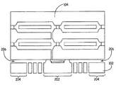
[0016]図1は、振動絶縁インターポーザ・ダイ102を含むシステム100の一例の斜視図である。振動絶縁インターポーザ・ダイ102(また本明細書で「インターポーザ・ダイ」または単に「インターポーザ」とも呼ばれる)は、チップ104(例えば、センサチップ)と基板106(例えば、回路基板)の間に取り付けられるように構成可能であり、基板106にチップ104を物理的に接続するものとして機能することができる。このように、チップ104はインターポーザ102に付けることができ、インターポーザ102は基板106に付けることができる。したがって、インターポーザ102は、半田、陽極結合、または他の材料などの任意の適切なダイアタッチを使用して基板106とチップ104に付けることができる。いくつかの例では、基板106とチップ104の間の電気的接続は、インターポーザ102を通して経路設定されることがある。これらの例では、インターポーザ102は、チップ104および基板106への電気接続と、チップ104と基板106の間の電気接続とを可能にする適切な配線、基板貫通ビア、エッジ相互接続、または他の相互接続、並びに導電性パッドなどであってもよい。インターポーザ102は、シリコン、ガラス、または他の基板などの任意の適切な材料で構成可能である。
FIG. 1 is a perspective view of an example of a
[0017]図2は、慣性測定ユニット(IMU)を一緒に構成することができる図1のインターポーザ102およびチップ104の一例の断面図である。この例では、チップ104は、少なくとも3個の微小電気機械システム(MEMS)ジャイロスコープと少なくとも3個のMEMS加速度計とを含むセンサチップを備えることができ、各ジャイロスコープおよび加速度計は3つの直交軸(例えば、X、Y、およびZ軸)のうちの1つに関して感知するように方向付けされている。チップ104は、インターポーザ102のチップ実装部202に取り付けることができる。インターポーザ102は、また、基板106に取り付けるように構成されたベース部204を含むことができる。
[0017] FIG. 2 is a cross-sectional view of an example of the
[0018]図3A〜3Cは、図1のインターポーザ102の例の上面図である。上で言及されたように、インターポーザ102は、ベース部204とチップ実装部202を含むことができる。インターポーザ102は、また、チップ実装部202をベース部204に接続する1つまたは複数の屈曲部302(例えば、バネ部材)を含むことができる。
[0018] FIGS. 3A-3C are top views of the example of the
[0019]1つまたは複数の屈曲部302は、ベース部204およびチップ実装部202に接続された細長い折畳み部材を含むことができる。それに加えて、1つまたは複数の屈曲部302の構造(例えば、折畳み構造)は、チップ実装部202がベース部204に対して動くことができるようにすることができる。この動きによって、インターポーザ102が、例えば基板106とチップ104の熱膨張係数の差によって生じる応力を吸収することができるようになる。その上、屈曲部302は、望ましい周波数より高い基板106中の周波数が実質的に吸収されてチップ104に伝えられないように設計することができる。1つの例では、インターポーザ102は、ほぼ100Hzより低い周波数がチップ104に伝えられ100Hzより高い周波数はインターポーザ102によって吸収されるように低いロールオフ周波数を持つことができる。いくつかの例では、インターポーザ102は、3つの直交軸のまわりの回転振動を含めて3つの直交軸に沿ったそのような振動を吸収するように設計されることがある。したがって、インターポーザ102は、チップ104に対して振動絶縁装置として働くことができる。
[0019] The one or
[0020]1つの例では、インターポーザ102は、チップ実装部202とベース部204の両方から外へ伸びる複数の突起304、306(例えば、フィン)を含むことができる。例えば、第1の複数の突起304は、互いに対向する面を持つように配置された複数の全体的に平らな構造、例えばフィンなどを備えることができる。さらに、対向面は、互いに接近し、かつチップ実装部202とベース部204の間の相対的な動きによって対向面が互いに近づいたり離れたりするように方向付けされることがある。2つの面によって流体(例えば、気体)が2つの面の間のギャップから押し出されたりギャップに引き込まれたりするようになるので、近づいたり離れたりする対向面のこの動きは、スクイーズ膜減衰を引き起こすことができる。
[0020] In one example, the
[0021]図4Aおよび4Bは、図3Aのインターポーザ102の一部の図であり、特に、複数の突起304、306を図示している。複数の突起は、ベース部204からチップ実装部202の方へ伸びる第1の複数の突起402‐1、402‐2と、チップ実装部202からベース部204の方へ伸びる第2の複数の突起404‐1、404‐2とを含む。図4Bに示されるように、第1および第2の複数の突起402‐1、402‐2、404‐1、404‐2はそれぞれ、全体的に平らなフィンを備える。全体的に平らなフィンは、ベース部204またはチップ実装部202からそれぞれ外へ垂直に伸びる。さらに、一方の側からの突起402‐1、402‐2は、反対方向に伸びる突起404‐1、404‐2の隙間に入り込んでいる。すなわち、ベース部204から伸びる突起402‐1、402‐2は、チップ実装部202から伸びる突起の間に伸び、チップ実装部202から伸びる突起404‐1、404‐2は、ベース部204から伸びる突起の間に伸びている。したがって、突起402‐1の面は、突起404‐1の面に対向している。このようにして、突起402‐1が突起404‐1に近づいたり離れたりするとき、突起402‐1、404‐1の間の流体は、突起間のギャップから押し出されたりギャップに引き込まれたりする。この流体の行動は、突起402‐1、404‐1の動きのスクイーズ膜減衰を引き起こす。このスクイーズ膜減衰は、互いに近づいたり離れたりする方向での突起402‐1、404‐1の動きによって起こるので、突起402‐1、404‐1は主にこの方向で減衰を与えるが、その方向に直交する方向ではほとんどまたは全く減衰を与えないことがある。したがって、インターポーザ102は、複数のサブセットの突起を含み、これらの複数のサブセットは、異なる方向で減衰を与えるように異なる方向に向けられる。例えば、第1のサブセットの突起402‐1は、第1の方向に向けられることがあり、第2のサブセットの突起402‐2は、第1の方向に対して直角の第2の方向に向けられることがある。ベース部204から伸びる第1のサブセットの突起402‐1は、チップ実装部202から伸びる対応する第3のサブセットの突起404‐1を有し、ベース部204から伸びる第2のサブセットの突起402‐2は、チップ実装部202から伸びる対応する第4のサブセットの突起404‐2を有する。したがって、第1のサブセット402‐1および第3のサブセット404‐1は、第1の方向で減衰を与えることができ、第2のサブセット402‐2および第4のサブセット404‐2は、第1の方向に対して直角の第2の方向で減衰を与えることができる。
[0021] FIGS. 4A and 4B are views of a portion of the
[0022]再び図3A〜3Cを参照すると、インターポーザ102は、様々な方向に向けられた突起304、306を含むことができる。例えば、図3Aのインターポーザ102では、突起304、306は矩形(例えば、正方形)のパターンで配置されている。図3Aで、第1の複数の突起304は、チップ実装部202から伸び、第2の複数の突起306は、ベース部204から伸びる。第1の複数の突起304は、第1の方向に伸びる第1のサブセット、第2の方向に伸びる第2のサブセット、第3の方向に伸びる第3のサブセット、および第4の方向に伸びる第4のサブセットを含み、第2の方向は第1の方向に対して直角であり、第3の方向は第1の方向と反対の方向へ延び、さらに第4の方向は第2の方向と反対の方向に延びる。また、第1、第2、第3、および第4の方向は、インターポーザ102によって形成される平面内にある。すなわち第1、第2、第3、および第4のサブセットの平らな表面は、インターポーザ102によって形成される平面に対して全体的に直角に方向付けされる。第2の複数の突起306は、第1のサブセットの隙間の中へ伸びる第5のサブセット、第2のサブセットの隙間の中へ伸びる第6のサブセット、第3のサブセットの隙間の中へ伸びる第7のサブセット、および第4のサブセットの隙間の中へ伸びる第8のサブセットを含む。したがって、第5のサブセットは第3の方向に伸び、第6のサブセットは第4の方向に伸び、第7のサブセットは第1の方向に伸び、第8のサブセットは第2の方向に伸びる。このようにして、インターポーザ102は、インターポーザ102によって形成される平面内の2つの直交方向でスクイーズ膜減衰を与えることができる。
[0022] Referring again to FIGS. 3A-3C, the
[0023]図3Bは、他の例を示し、突起304、306は円形パターンに配置されている。したがって、第1の複数の突起304は、チップ実装部202から半径方向外向きに伸びる。第2の複数の突起306は、ベース部204から半径方向内向きに伸びる。図示のように、第2の複数の突起306は、第1の複数の突起304の隙間の中へ伸びている。4個の屈曲部302が、ベース204をチップ実装部202にフレキシブルに接続するのが示されている。しかし、他の数および/または向きの屈曲部が使用可能である。したがって、ベース部204に対するチップ実装部202の回転、並びにほとんどの方向でのインターポーザ202の面に沿った横方向の動きは、突起304、306によって減衰されることがある。
[0023] FIG. 3B shows another example, where the
[0024]図3Cは、さらに他の例を示し、突起304、306は、円形パターンに配置されて、チップ実装部202から半径方向外向きおよび内向きの動きを減衰させるように方向付けされている。第1の複数の突起304は、チップ実装部202から伸び、ベース部204から伸びる第2の複数の突起306の対応する面に対向する面を持っている。これらの面は、チップ実装部に対して半径方向外向きおよび内向きの動きを減衰させるように方向付けされている。4個の屈曲部302が、ベース部204をチップ実装部202にフレキシブルに接続するのが示されている。しかし、他の数および/または向きの屈曲部が使用可能である。
[0024] FIG. 3C shows yet another example, where the
[0025]突起304、306のパターン、向き、数および形状寸法の特定の例が図3A〜3Cに示されている。しかし、理解されるべきことであるが、突起304、306の他のパターン、向き、数、および形状寸法が使用可能である。1つの例では、突起304、306は、対向面が互いに10ミクロン以下で離れているように配置される。他の例では、突起304、306は、対向面が互いに5ミクロン以下で離れているように配置される。これらの距離は、望ましいスクイーズ膜減衰を達成するために使用可能である。
[0025] A specific example of the pattern, orientation, number and geometry of the
[0026]再び図2を参照すると、インターポーザ102とチップ104の間に形成されるギャップ206は、インターポーザ102によって形成される平面に対して直角の方向でスクイーズ膜減衰を可能にすることができる。すなわち、チップ実装部202に対するベース部204の動き(例えば、図2に示されるように上下に)によって、ギャップ206内の流体(例えば、空気)がギャップ206から押し出されたりギャップに引き込まれたりするようになる。この流体の動きは、インターポーザ102によって形成される平面に対して直角の方向(例えば、z軸)の動きをスクイーズ膜減衰させるように働くことができる。1つの例では、インターポーザ102とセンサチップ104の間のギャップ206は、10ミクロン以下である。他の例では、インターポーザ102とセンサチップ104の間のギャップ206は、5ミクロン以下である。
[0026] Referring again to FIG. 2, the
[0027]再び図3Aを参照すると、1つの例では、ベース部204は、インターポーザ102の周辺部を構成し、チップ実装部202はインターポーザ102の内部領域を構成する。突起304、306は、チップ実装部202とベース部204の間に配置される。1つの例では、突起304、306の間に形成された1つまたは複数の開口(例えば、ギャップ)は、空気にさらされる(例えば、インターポーザ102を取り囲む環境にさらされる)。空気が突起304、306の間でスクイーズ膜減衰に使用される例では、空気は温度につれて比較的ゆっくり変化する(液体またはエラストマに比べて)ので、減衰は温度範囲にわたって比較的一定であることがある。他の例では、チップ実装部がインターポーザの周辺部を構成することがあり、ベース部がインターポーザの内部領域を構成することがある。すなわち、いくつかの例では、チップ104は、インターポーザの周辺部に取り付けられることがあり、インターポーザは、内部領域の基板106に取り付けられることがある。他の例では、チップ実装部およびベース部の他の配置が使用可能である。
Referring back to FIG. 3A, in one example, the
[0028]1つの例では、屈曲部302は、屈曲部302の共振を減衰させるために重合体を含む。いずれにしても、突起304、306は、チップ実装部202とベース部204の間の動き(例えば、振動)を減衰させることができる。
[0028] In one example, the
[0029]1つの例では、インターポーザ102は、半導体プロセスを使用して製作されることがある。例えば、インターポーザ102は、複数の将来インターポーザ・ダイを有するブランクウェーハから始めて形成されることがある。インターポーザ・ダイの各々は、ベース部204とチップ実装部202の間に開口(例えば、ギャップ)を形成するようにエッチングされることがある。このエッチングは、また、突起304、306および屈曲部302を画定することができる。次に、ウェーハは、個々のインターポーザ・ダイを形成するように単体化されることがある。次に、インターポーザ・ダイ102は、他のチップ104(例えば、センサチップ)および/または基板106(例えば、回路基板)に付けられてもよい(例えば、接着される)。
[0029] In one example, the
[0030]1つの例では、インターポーザ102は、インターポーザ102を貫通してチップ104を基板106に電気的に結合する電気相互接続を含むことがある。1つの例では、電気相互接続は、1つまたは複数の配線406を1つまたは複数の屈曲部302上に含むことができる。屈曲部上の配線406は、チップ実装部202上の接続部408(例えば、ダイパッド)をベース部204上の基板貫通ビア(TSV)410と結合することができる。ダイパッド408は、チップ104に結合するように構成されることがあり、TSV410は、インターポーザ102の底部側で基板106に結合するように構成されることがある。配線406は、屈曲部302に関連した動きに耐えるように構成可能である。したがって、チップ104は、インターポーザ102の電気相互接続を通して基板106に電気的に結合可能である。他の例では、インターポーザ102の縁部の垂直相互接続を含めて他の電気相互接続が使用されることがある。
In one example, the
[0031]図5は、振動絶縁インターポーザ・ダイを有するIMU706を含む電子装置700のブロック図である。システム700は、1つまたは複数の記憶装置704に結合された1つまたは複数の処理装置702を含むことができる。1つまたは複数の記憶装置は、1つまたは複数の処理装置702によって実行されたときハイブリッドまたは慣性ナビゲーション解決法を行うようなナビゲーション機能を処理装置702に実現させる命令を含むことができる。1つまたは複数の処理装置702は、また、インターポーザ・ダイ102のようなインターポーザ・ダイを含むことができるIMU104のようなIMU706に結合されることがある。したがって、IMU706のセンサは、基板(例えば、回路基板)からの振動および温度変化から分離されることがある。電子装置700は、また、他の装置と信号の送受信をするための入力および/または出力ポート708を含むことができる。いくつかの例では、電子装置700は、また、衛星ナビゲーションシステム受信機のような他のセンサを含むことができる。1つの例では、電子装置700は、航空機、自動車、携帯電話、または慣性データが望ましい他の装置のようなもっと大きな他の装置に一体化されるように構成されることがある。
[0031] FIG. 5 is a block diagram of an electronic device 700 that includes an
[0032]1つまたは複数の処理装置702は、中央処理装置(CPU)、マイクロコントローラ、マイクロプロセッサ(例えば、ディジタル信号処理装置(DSP))、フィールドプログラマブルゲートアレイ(FPGA)、用途特定集積回路(ASIC)および他の処理装置などであることがある。1つまたは複数の処理装置702および電子装置700が、或る特定の行為を行うように「構成」されることがあり、そのとき、1つまたは複数の記憶装置704は、1つまたは複数の処理装置702によって実行されたときその或る特定の行為をその1つまたは複数の処理装置702に行わせる命令を含んでいる。この命令は、例えば、ナビゲーションシステムの機能を実現することがある。この命令は、プロセッサ読取り可能命令および/またはデータ構造を格納するために使用される任意の適切なプロセッサ読取り可能媒体に格納されることがある。このプロセッサ読取り可能媒体は、1つまたは複数の記憶装置704および/または他の適切な媒体を含むことができる。適切なプロセッサ読取り可能媒体は、磁気または光媒体のような有形の媒体などであることがある。
[0032] One or
[0033]本明細書で特定の実施形態が図示され説明されたが、同じ目的を達成するために計画されるどんな構成でも、示された特定の実施形態の代わりに用いられる可能性があることを、当業者は理解するであろう。したがって、この発明は特許請求の範囲およびその均等物によってのみ限定されることが、明白に意図されている。
[形態1]
ベース部と、
チップ実装部と、
前記ベース部を前記チップ実装部に接続する1つまたは複数の屈曲部と、
前記ベース部から前記チップ実装部の方へ伸びる第1の複数の突起と、
前記チップ実装部から前記ベース部の方へ伸びて、第1の複数の突起によって形成される隙間に入り込んでいる第2の複数の突起と
を備えるインターポーザ・チップ。
[形態2]
形態1に記載のインターポーザ・チップ装置であって、前記第1および第2の複数の突起が、前記ベース部に対する前記チップ実装部の動きをスクイーズ膜減衰させるよう構成されているインターポーザ・チップ装置。
[形態3]
形態1に記載のインターポーザ・チップ装置であって、前記第1および第2の複数の突起は、前記第1の複数の突起の面が前記第2の複数の突起の面に対向するように配置された全体的に平らな構造を含み、
前記第1および第2の複数の突起の前記全体的に平らな構造が、前記インターポーザ・チップによって形成される平面に対して直角であるインターポーザ・チップ装置。
[0033] While specific embodiments have been illustrated and described herein, any configuration planned to accomplish the same purpose may be used in place of the specific embodiments shown. Will be understood by those skilled in the art. Therefore, it is manifestly intended that this invention be limited only by the claims and the equivalents thereof.
[Form 1]
A base part;
A chip mounting part;
One or more bent portions connecting the base portion to the chip mounting portion;
A plurality of first protrusions extending from the base portion toward the chip mounting portion;
An interposer chip comprising: a second plurality of protrusions extending from the chip mounting portion toward the base portion and entering a gap formed by the first plurality of protrusions.
[Form 2]
2. The interposer chip device according to claim 1, wherein the first and second plurality of protrusions are configured to attenuate the movement of the chip mounting portion relative to the base portion by squeezing a film.
[Form 3]
The interposer chip device according to the first aspect, wherein the first and second plurality of protrusions are arranged such that surfaces of the first plurality of protrusions face surfaces of the second plurality of protrusions. Including a generally flat structure
An interposer chip device wherein the generally flat structure of the first and second plurality of protrusions is perpendicular to a plane formed by the interposer chip.
100 振動絶縁インターポーザ・ダイを含むシステム
102 振動絶縁インターポーザ・ダイ
104 チップ
106 基板
202 チップ実装部
204 ベース部
206 ギャップ
302 屈曲部
304、306 突起
402‐1、402‐2 突起
404‐1、404‐2 突起
406 配線
408 接続部
410 基板貫通ビア
700 電子装置
702 処理装置
704 記憶装置
706 IMU
708 入出力ポート
DESCRIPTION OF
708 I / O port
Claims (3)
チップ実装部と、
前記ベース部を前記チップ実装部に接続する1つまたは複数の屈曲部と、
前記ベース部から前記チップ実装部の方へ伸びる第1の複数の突起と、
前記チップ実装部から前記ベース部の方へ伸びて、第1の複数の突起によって形成される隙間に入り込んでいる第2の複数の突起と
を備えるインターポーザ・チップ。 A base part;
A chip mounting part;
One or more bent portions connecting the base portion to the chip mounting portion;
A plurality of first protrusions extending from the base portion toward the chip mounting portion;
An interposer chip comprising: a second plurality of protrusions extending from the chip mounting portion toward the base portion and entering a gap formed by the first plurality of protrusions.
前記第1および第2の複数の突起の前記全体的に平らな構造が、前記インターポーザ・チップによって形成される平面に対して直角であるインターポーザ・チップ装置。 2. The interposer chip device according to claim 1, wherein the first and second plurality of protrusions are arranged such that a surface of the first plurality of protrusions faces a surface of the second plurality of protrusions. Including a generally flat structure arranged,
An interposer chip device wherein the generally flat structure of the first and second plurality of protrusions is perpendicular to a plane formed by the interposer chip.
Applications Claiming Priority (4)
| Application Number | Priority Date | Filing Date | Title |
|---|---|---|---|
| US41648510P | 2010-11-23 | 2010-11-23 | |
| US61/416,485 | 2010-11-23 | ||
| US13/299,485 | 2011-11-18 | ||
| US13/299,485 US9227835B2 (en) | 2010-11-23 | 2011-11-18 | Vibration isolation interposer die |
Publications (2)
| Publication Number | Publication Date |
|---|---|
| JP2012146958A JP2012146958A (en) | 2012-08-02 |
| JP5860270B2 true JP5860270B2 (en) | 2016-02-16 |
Family
ID=44992800
Family Applications (1)
| Application Number | Title | Priority Date | Filing Date |
|---|---|---|---|
| JP2011255390A Expired - Fee Related JP5860270B2 (en) | 2010-11-23 | 2011-11-22 | Vibration isolation interposer die |
Country Status (4)
| Country | Link |
|---|---|
| US (1) | US9227835B2 (en) |
| EP (1) | EP2455329B1 (en) |
| JP (1) | JP5860270B2 (en) |
| CN (1) | CN102530827A (en) |
Families Citing this family (20)
| Publication number | Priority date | Publication date | Assignee | Title |
|---|---|---|---|---|
| US8896074B2 (en) * | 2012-01-26 | 2014-11-25 | The Charles Stark Draper Laboratory, Inc. | MEMS vibration isolation system and method |
| US20130264755A1 (en) * | 2012-04-05 | 2013-10-10 | Honeywell International Inc. | Methods and systems for limiting sensor motion |
| DE102013222966A1 (en) * | 2013-11-12 | 2015-05-28 | Robert Bosch Gmbh | inertial sensor |
| US9425125B2 (en) | 2014-02-20 | 2016-08-23 | Altera Corporation | Silicon-glass hybrid interposer circuitry |
| DE102014210912A1 (en) * | 2014-06-06 | 2015-12-17 | Robert Bosch Gmbh | Interposer for mounting a vertically hybrid integrated component on a component carrier |
| US20160039664A1 (en) * | 2014-08-06 | 2016-02-11 | Honeywell International Inc. | Monolithic integration of stress isolation feautures in a microelectromechanical system (mems) structure |
| US9574959B2 (en) * | 2014-09-02 | 2017-02-21 | Apple Inc. | Various stress free sensor packages using wafer level supporting die and air gap technique |
| US10167189B2 (en) | 2014-09-30 | 2019-01-01 | Analog Devices, Inc. | Stress isolation platform for MEMS devices |
| US10131535B2 (en) * | 2015-05-22 | 2018-11-20 | Honeywell International Inc. | Monolithic fabrication of thermally isolated microelectromechanical system (MEMS) devices |
| US10211757B2 (en) | 2015-08-04 | 2019-02-19 | Mems Drive, Inc. | Multi-directional actuator |
| FR3048781B1 (en) * | 2016-03-11 | 2018-03-16 | Commissariat A L'energie Atomique Et Aux Energies Alternatives | LINEAR ACCELEROMETER AMORTI |
| EP3260821B1 (en) * | 2016-06-21 | 2019-09-11 | ams International AG | Sensor package and method of producing the sensor package |
| US10611628B2 (en) | 2016-12-29 | 2020-04-07 | Epack, Inc. | MEMS isolation platform with three-dimensional vibration and stress isolation |
| GB2560192A (en) * | 2017-03-03 | 2018-09-05 | Atlantic Inertial Systems Ltd | Vibration damping mount |
| US20190169018A1 (en) * | 2017-12-05 | 2019-06-06 | Invensense, Inc. | Stress isolation frame for a sensor |
| US20190241428A1 (en) * | 2018-02-06 | 2019-08-08 | Epack, Inc. | Space-efficient planar interposer for environment-resistant packaging |
| CN108609576B (en) * | 2018-04-09 | 2019-12-31 | 合肥工业大学 | Double-layer vibration isolation structure for vibration isolation of MEMS device and preparation method |
| GB2575694A (en) * | 2018-07-20 | 2020-01-22 | Atlantic Inertial Systems Ltd | Sensor packages |
| US11417611B2 (en) | 2020-02-25 | 2022-08-16 | Analog Devices International Unlimited Company | Devices and methods for reducing stress on circuit components |
| US11981560B2 (en) | 2020-06-09 | 2024-05-14 | Analog Devices, Inc. | Stress-isolated MEMS device comprising substrate having cavity and method of manufacture |
Family Cites Families (22)
| Publication number | Priority date | Publication date | Assignee | Title |
|---|---|---|---|---|
| US4129042A (en) | 1977-11-18 | 1978-12-12 | Signetics Corporation | Semiconductor transducer packaged assembly |
| US4558397A (en) * | 1983-12-19 | 1985-12-10 | Amp Incorporated | Interposer connector for surface mounting a ceramic chip carrier to a printed circuit board |
| GB9009753D0 (en) * | 1990-05-01 | 1990-06-20 | Bt & D Technologies Ltd | Photo detectors |
| US5138430A (en) * | 1991-06-06 | 1992-08-11 | International Business Machines Corporation | High performance versatile thermally enhanced IC chip mounting |
| DE10010975B4 (en) * | 2000-03-07 | 2010-04-08 | Robert Bosch Gmbh | Micromechanical component |
| US6330102B1 (en) * | 2000-03-24 | 2001-12-11 | Onix Microsystems | Apparatus and method for 2-dimensional steered-beam NxM optical switch using single-axis mirror arrays and relay optics |
| EP1292834B1 (en) * | 2000-06-20 | 2005-11-30 | Nanonexus, Inc. | Systems for testing integrated circuits |
| JP2002071353A (en) | 2000-09-01 | 2002-03-08 | Ngk Insulators Ltd | Angular velocity measuring instrument |
| JP2002195834A (en) * | 2000-12-27 | 2002-07-10 | Murata Mfg Co Ltd | Physical quantity detector |
| US6754584B2 (en) * | 2001-02-28 | 2004-06-22 | Enpoint, Llc | Attitude measurement using a single GPS receiver with two closely-spaced antennas |
| US6937479B2 (en) | 2001-08-21 | 2005-08-30 | The Charles Stark Draper Laboratory, Inc. | Sensor isolation system |
| JP4724488B2 (en) * | 2005-02-25 | 2011-07-13 | 日立オートモティブシステムズ株式会社 | Integrated microelectromechanical system |
| US7562573B2 (en) * | 2005-07-21 | 2009-07-21 | Evigia Systems, Inc. | Integrated sensor and circuitry and process therefor |
| DE102006022807A1 (en) | 2006-05-16 | 2007-11-22 | Robert Bosch Gmbh | Chip housing with reduced vibration coupling |
| WO2009031285A1 (en) * | 2007-09-03 | 2009-03-12 | Panasonic Corporation | Inertia force sensor |
| DE102007052367A1 (en) * | 2007-11-02 | 2009-05-07 | Robert Bosch Gmbh | Micromechanical system |
| CN101271124B (en) * | 2008-05-16 | 2010-09-29 | 中国科学院上海微系统与信息技术研究所 | L-beam piezoresistance type micro-accelerometer and production method thereof |
| DE102009000574B4 (en) | 2009-02-03 | 2017-07-27 | Robert Bosch Gmbh | sensor device |
| JP2010223952A (en) | 2009-02-24 | 2010-10-07 | Seiko Epson Corp | Acceleration sensor and electronic apparatus |
| CN101792108B (en) * | 2010-03-16 | 2011-12-21 | 杭州电子科技大学 | Large capacitance micro inertial sensor based on slide-film damping and manufacturing method thereof |
| US8941222B2 (en) * | 2010-11-11 | 2015-01-27 | Advanced Semiconductor Engineering Inc. | Wafer level semiconductor package and manufacturing methods thereof |
| US8896074B2 (en) * | 2012-01-26 | 2014-11-25 | The Charles Stark Draper Laboratory, Inc. | MEMS vibration isolation system and method |
-
2011
- 2011-11-18 US US13/299,485 patent/US9227835B2/en active Active
- 2011-11-22 JP JP2011255390A patent/JP5860270B2/en not_active Expired - Fee Related
- 2011-11-22 EP EP11190205.2A patent/EP2455329B1/en active Active
- 2011-11-23 CN CN2011104568373A patent/CN102530827A/en active Pending
Also Published As
| Publication number | Publication date |
|---|---|
| EP2455329B1 (en) | 2014-09-24 |
| US20120130671A1 (en) | 2012-05-24 |
| US9227835B2 (en) | 2016-01-05 |
| JP2012146958A (en) | 2012-08-02 |
| CN102530827A (en) | 2012-07-04 |
| EP2455329A3 (en) | 2014-01-01 |
| EP2455329A2 (en) | 2012-05-23 |
Similar Documents
| Publication | Publication Date | Title |
|---|---|---|
| JP5860270B2 (en) | Vibration isolation interposer die | |
| US10611628B2 (en) | MEMS isolation platform with three-dimensional vibration and stress isolation | |
| US8896074B2 (en) | MEMS vibration isolation system and method | |
| US10131538B2 (en) | Mechanically isolated MEMS device | |
| JP2018146569A (en) | Vibration damping mount | |
| US9261363B2 (en) | Yaw rate sensor | |
| US11650221B2 (en) | MEMS tri-axial accelerometer with one or more decoupling elements | |
| KR20070046001A (en) | Mems sensor systems and methods | |
| US9140550B2 (en) | Inertial micro-sensor of angular displacements | |
| EP2840375A1 (en) | Device with a micro- or nanoscale structure | |
| JPWO2010032818A1 (en) | MEMS sensor and detection apparatus | |
| US20160229689A1 (en) | Packaged Microchip with Patterned Interposer | |
| JP2007218902A (en) | Discrete stress isolator | |
| TWI471258B (en) | Mikromechanisches system | |
| US9731958B2 (en) | Microelectromechanical system and fabricating process having decoupling structure that includes attaching element for fastening to carrier | |
| US10843917B2 (en) | Micromechanical device having a decoupled micromechanical structure | |
| US9963339B2 (en) | Sensor device | |
| US9123883B2 (en) | Vibration device | |
| JP2014215294A (en) | MEMS element | |
| CN219174214U (en) | Packaging structure, MEMS device and terminal equipment | |
| WO2014030492A1 (en) | Inertial force sensor | |
| CN101880022B (en) | Anti-vibration device and preparation method thereof | |
| KR101496949B1 (en) | Inertial sensor having vibration proof function and fabrication method thereof |
Legal Events
| Date | Code | Title | Description |
|---|---|---|---|
| A621 | Written request for application examination |
Free format text: JAPANESE INTERMEDIATE CODE: A621 Effective date: 20141117 |
|
| A131 | Notification of reasons for refusal |
Free format text: JAPANESE INTERMEDIATE CODE: A131 Effective date: 20150416 |
|
| A601 | Written request for extension of time |
Free format text: JAPANESE INTERMEDIATE CODE: A601 Effective date: 20150716 |
|
| A521 | Written amendment |
Free format text: JAPANESE INTERMEDIATE CODE: A523 Effective date: 20150729 |
|
| TRDD | Decision of grant or rejection written | ||
| A01 | Written decision to grant a patent or to grant a registration (utility model) |
Free format text: JAPANESE INTERMEDIATE CODE: A01 Effective date: 20151119 |
|
| A61 | First payment of annual fees (during grant procedure) |
Free format text: JAPANESE INTERMEDIATE CODE: A61 Effective date: 20151218 |
|
| R150 | Certificate of patent or registration of utility model |
Ref document number: 5860270 Country of ref document: JP Free format text: JAPANESE INTERMEDIATE CODE: R150 |
|
| LAPS | Cancellation because of no payment of annual fees |