JP5834412B2 - Infrared sensor and infrared array sensor - Google Patents
Infrared sensor and infrared array sensor Download PDFInfo
- Publication number
- JP5834412B2 JP5834412B2 JP2011008163A JP2011008163A JP5834412B2 JP 5834412 B2 JP5834412 B2 JP 5834412B2 JP 2011008163 A JP2011008163 A JP 2011008163A JP 2011008163 A JP2011008163 A JP 2011008163A JP 5834412 B2 JP5834412 B2 JP 5834412B2
- Authority
- JP
- Japan
- Prior art keywords
- mosfet
- sensor
- current source
- current
- gate
- Prior art date
- Legal status (The legal status is an assumption and is not a legal conclusion. Google has not performed a legal analysis and makes no representation as to the accuracy of the status listed.)
- Expired - Fee Related
Links
Images

Classifications
-
- G—PHYSICS
- G01—MEASURING; TESTING
- G01J—MEASUREMENT OF INTENSITY, VELOCITY, SPECTRAL CONTENT, POLARISATION, PHASE OR PULSE CHARACTERISTICS OF INFRARED, VISIBLE OR ULTRAVIOLET LIGHT; COLORIMETRY; RADIATION PYROMETRY
- G01J5/00—Radiation pyrometry, e.g. infrared or optical thermometry
- G01J5/10—Radiation pyrometry, e.g. infrared or optical thermometry using electric radiation detectors
- G01J5/20—Radiation pyrometry, e.g. infrared or optical thermometry using electric radiation detectors using resistors, thermistors or semiconductors sensitive to radiation, e.g. photoconductive devices
- G01J5/22—Electrical features thereof
- G01J5/24—Use of specially adapted circuits, e.g. bridge circuits
-
- G—PHYSICS
- G01—MEASURING; TESTING
- G01J—MEASUREMENT OF INTENSITY, VELOCITY, SPECTRAL CONTENT, POLARISATION, PHASE OR PULSE CHARACTERISTICS OF INFRARED, VISIBLE OR ULTRAVIOLET LIGHT; COLORIMETRY; RADIATION PYROMETRY
- G01J5/00—Radiation pyrometry, e.g. infrared or optical thermometry
- G01J2005/0077—Imaging
Landscapes
- Physics & Mathematics (AREA)
- General Physics & Mathematics (AREA)
- Spectroscopy & Molecular Physics (AREA)
- Photometry And Measurement Of Optical Pulse Characteristics (AREA)
- Semiconductor Integrated Circuits (AREA)
Description
本発明は、赤外線センサー及び赤外線アレイセンサーに関し、特に、サブスレッショルド領域で動作するセンサーMOSFET(Metal-Oxide-Semiconductor Field-Effect Transistor)を備えた熱型赤外線センサー及び赤外線アレイセンサーに関する。 The present invention relates to an infrared sensor and an infrared array sensor, and more particularly, to a thermal infrared sensor and an infrared array sensor including a sensor MOSFET (Metal-Oxide-Semiconductor Field-Effect Transistor) that operates in a subthreshold region.
熱型赤外線センサーとして、温度検知部をサブスレッショルド領域で動作させるMOSFETで構成したものがある(例えば特許文献1を参照。)。
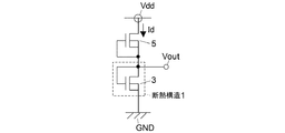
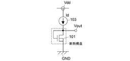
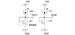
図11は従来の熱型赤外線センサーの構造を説明するための回路図である。
赤外線センサーは、センサーMOSFET101と定電流源103で構成されている。センサーMOSFET101は定電流源103によって与えられる電流Idで定電流駆動され、サブスレッショルド領域で動作しており、センサー出力電圧Voutを出力している。
As a thermal infrared sensor, there is one configured by a MOSFET that operates a temperature detection unit in a sub-threshold region (see, for example, Patent Document 1).
FIG. 11 is a circuit diagram for explaining the structure of a conventional thermal infrared sensor.
The infrared sensor includes a
センサーMOSFET1は、赤外線入射に対する感度向上のため断熱構造体上に形成されている。ここで、断熱構造体とは、センサーMOSFETを基板に対して熱的に分離された構造体であり、一般的には、センサーMOSFET1が形成された薄膜状のメンブレン部を複数本の梁で中空状態に支持する構造となっている。
The
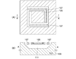
図12は、断熱構造体の一例を説明するための概略図であり、(A)は平面図、(B)は(A)のA−A’位置での断面図である。
断熱構造体はメンブレン部105を二本の梁107で支持した構造となっており、基板109とメンブレン部105との間に空間111が形成されている。図12で示した断熱構造以外にも様々な形状の断熱構造体があり、断熱構造体はこの構造に限定されるものではない。
12A and 12B are schematic views for explaining an example of the heat insulating structure, in which FIG. 12A is a plan view and FIG. 12B is a cross-sectional view taken along the line AA ′ in FIG.
The heat insulating structure has a structure in which the
センサーMOSFET101はメンブレン105中に形成されており、センサーMOSFET101は基板109から熱的に分離されている。
メンブレン部105に赤外線が入射すると、メンブレン部105の温度が上昇し、それに伴い、メンブレン部105に形成されたセンサーMOSFET101の温度も上昇する。センサーMOSFET101に温度変化が生じると、MOSFET101のしきい値電圧が変化し、その変化がセンサー出力電圧Voutの変化として取り出される。つまり、熱型赤外線センサーは、センサーMOSFET101を温度センサーとして利用し、赤外線入射による微小な温度変化を捉えて、赤外線を検出している。
The
When infrared rays are incident on the
ところが、熱型赤外線センサーには、温度検知部をサブスレッショルド領域で動作させるMOSFETで構成した熱型赤外線センサーに限らず、周囲温度の影響によってセンサーの出力電圧のDC(直流電圧)レベルが変化するという問題があった。すなわち、熱型赤外線センサーの基本原理は温度センサーであるため、赤外線入射時以外でも、周囲温度の変化によって、センサーMOSFET101自体の温度が変化するとセンサー出力電圧Voutが変化してしまうという問題があった。また、センサーMOSFET101は、赤外線に対する感度向上のためにしきい値電圧の温度係数を大きくする必要があるが、しきい値電圧の温度係数を大きくすると、周囲温度の影響によるセンサー出力電圧Voutの変化も大きくなるという問題があった。
However, the thermal infrared sensor is not limited to the thermal infrared sensor configured by the MOSFET that operates the temperature detection unit in the subthreshold region, but the DC (direct current voltage) level of the output voltage of the sensor changes due to the influence of the ambient temperature. There was a problem. That is, since the basic principle of the thermal infrared sensor is a temperature sensor, there is a problem that the sensor output voltage Vout changes when the temperature of the
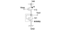
図13は、従来の熱型赤外線センサーの一つで定電流源をP型のMOSFET113で構成した例を説明するための回路図である。
このような構成でも、N型のMOSFETで構成されたセンサーMOSFET101とP型のMOSFETで構成された電流源MOSFET113の温度特性が異なるため、図11に示した構成の場合と同様に、周囲温度の変化によって、センサー出力電圧VoutのDCレベルが変化する。
FIG. 13 is a circuit diagram for explaining an example in which a constant current source is constituted by a P-
Even in such a configuration, since the temperature characteristics of the
この問題の解決策の一つとして、赤外線センサーをペルチェ素子等の電気的な冷却素子によって常に一定の温度に制御する方法がある。しかし、この方法では、冷却素子や温度制御機能を付加することにより、センサー部の構造が複雑化及び大型化し、製造コストが増大するという問題があった。さらに、ペルチェ素子やそれを制御するシステムの消費電力が大きく、システム全体としての消費電力が大きくなるという問題があった。 As a solution to this problem, there is a method in which the infrared sensor is always controlled at a constant temperature by an electric cooling element such as a Peltier element. However, this method has a problem in that the structure of the sensor unit is complicated and enlarged by adding a cooling element and a temperature control function, and the manufacturing cost increases. Furthermore, there is a problem that the power consumption of the Peltier element and the system that controls the Peltier element is large, and the power consumption of the entire system increases.
別の解決策として、参照センサーを配置する方法がある。
図14は、参照センサーを備えた赤外線センサーを説明するための回路図である。
図11に示したセンサーMOSFET101と定電流源103に加えて、参照用センサーMOSFET115と定電流源117が設けられている。参照用センサーMOSFET115はセンサーMOSFET101と同じ構造で形成され、定電流源117は定電流源103と同じ構造で形成されている。参照用センサーMOSFET115は断熱構造体とは異なる位置に形成されている。参照用センサーMOSFET115は定電流源117によって与えられる電流Idで定電流駆動され、サブスレッショルド領域で動作しており、センサー出力電圧Vout2を出力している。センサーMOSFET101のセンサー出力電圧Vout1と参照用センサーMOSFET115のセンサー出力電圧Vout2の差をとることにより、周囲温度の変化に起因する影響を排除できる。
Another solution is to place a reference sensor.
FIG. 14 is a circuit diagram for explaining an infrared sensor including a reference sensor.
In addition to the
この方法を用いれば、冷却素子等を使用する必要はない。しかし、センサー出力電圧Vout1,Vout2のDCレベルは周囲温度の変化にともなって変化する。特に、センサーMOSFET101,115の温度感度が大きく、周囲温度の変化が大きい場所で当該赤外線センサーを使用する場合には、温度変化に起因するセンサー出力電圧Vout1,Vout2のDCレベル変化を考慮して、センサーMOSFET101,115やセンサー出力電圧Vout1,Vout2の差をとる後段回路に与える電源電圧を高くする必要がある。このように、この方法は、センサーの使用環境温度範囲が広くなるにしたがって、センサー出力信号と参照温度センサー出力信号のDCレベル変化が大きくなるため、次段の回路の電源電圧を高くする必要があり、低電圧動作に限界があるという問題があった。また、センサー素子の感度が高くなるほど、センサー出力信号のDCレベル変化が大きくなるため、次段の回路の電源電圧をより高くする必要があり、高感度でかつ低電圧動作させることが難しいという問題があった。
If this method is used, it is not necessary to use a cooling element or the like. However, the DC levels of the sensor output voltages Vout1 and Vout2 change as the ambient temperature changes. In particular, when the infrared sensor is used in a place where the temperature sensitivity of the
本発明は、周囲温度が変化した場合でも、ペルチェ素子等の電気的な冷却素子を使用することなく、熱型赤外線センサーの出力電圧のDCレベル変化を小さくすることを目的とする。 An object of the present invention is to reduce the DC level change of the output voltage of the thermal infrared sensor without using an electrical cooling element such as a Peltier element even when the ambient temperature changes.
本発明にかかる赤外線センサーは、センサーMOSFETと、上記センサーMOSFETに直列接続され、上記センサーMOSFETを定電流駆動させるための定電流源を構成する電流源MOSFETを備え、上記センサーMOSFETと上記電流源MOSFETの間の端子がセンサー出力端子を構成している。上記センサーMOSFETは断熱構造体上に配置され、上記電流源MOSFETは上記断熱構造体の外部に配置されている。上記センサーMOSFET及び上記電流源MOSFETは同じ導電型のMOSFETからなり、かつサブスレッショルド領域で動作される。 An infrared sensor according to the present invention includes a sensor MOSFET and a current source MOSFET that is connected in series to the sensor MOSFET and constitutes a constant current source for driving the sensor MOSFET with a constant current. The sensor MOSFET and the current source MOSFET The terminals between are configured as sensor output terminals. The sensor MOSFET is disposed on the heat insulating structure, and the current source MOSFET is disposed outside the heat insulating structure. The sensor MOSFET and the current source MOSFET are composed of MOSFETs of the same conductivity type, and are operated in the subthreshold region.
周囲温度が変化した場合、本発明の赤外線センサー全体の温度が変化する。センサーMOSFETと電流源MOSFET2は同じ導電型のMOSFETで形成されているので、温度変化に対して両MOSFETの特性がほぼ等しく変化する。一方、赤外線が入射した場合には、断熱構造体部分のみに温度変化が生じるため、断熱構造体上に形成されたセンサーMOSFETのみの特性が変化し、赤外線を検知することが可能である。
When the ambient temperature changes, the temperature of the entire infrared sensor of the present invention changes. Since the sensor MOSFET and the
本発明にかかる赤外線センサーにおいて、上記センサーMOSFETは複数段直列に接続されているようにしてもよい。 In the infrared sensor according to the present invention, the sensor MOSFETs may be connected in series in a plurality of stages.
また、上記センサーMOSFETはゲートとドレインが短絡され、上記電流源MOSFETはゲートとソースが短絡されているようにしてもよい。この態様において、上記センサーMOSFETと上記電流源MOSFETでゲート−ソース間電圧が同一である場合に上記センサーMOSFETのサブスレッショルド領域電流が上記電流源MOSFETのサブスレッショルド領域電流よりも小さくなるように設定される。 The sensor MOSFET may have a gate and a drain short-circuited, and the current source MOSFET may have a gate and a source short-circuited. In this aspect, when the gate-source voltage is the same in the sensor MOSFET and the current source MOSFET, the subthreshold region current of the sensor MOSFET is set to be smaller than the subthreshold region current of the current source MOSFET. The
上記センサーMOSFETはゲートとドレインが短絡され、上記電流源MOSFETはゲートとソースが短絡されている態様において、上記電流源MOSFETと上記センサーMOSFETは、同一構造のペアトランジスタであるか、チャネル不純物濃度以外が同一構造のトランジスタであるか、ゲート不純物濃度以外が同一構造のトランジスタである例を挙げることができる。ただし、本発明において、電流源MOSFETとセンサーMOSFETの構造はこれらの例に限定されない。 In the aspect in which the gate and the drain of the sensor MOSFET are short-circuited and the gate and the source of the current source MOSFET are short-circuited, the current source MOSFET and the sensor MOSFET are a pair transistor having the same structure or other than the channel impurity concentration Are transistors having the same structure, or transistors having the same structure except for the gate impurity concentration. However, in the present invention, the structures of the current source MOSFET and the sensor MOSFET are not limited to these examples.
本発明の赤外線センサーにおいて、上記定電流源は、上記断熱構造体の外部に配置され、サブスレッショルド領域で上記電流源MOSFETが流す電流以上の電流を流すことができるN型の第2電流源MOSFET又はP型の第3電流源MOSFETをさらに備えているようにしてもよい。上記第2電流源MOSFETが配置される場合、上記センサーMOSFET及び上記電流源MOSFETはN型で構成され、上記第2電流源MOSFETは、上記電流源MOSFETの電源側に直列に接続され、ゲートとソースが短絡され、かつバックゲートが上記センサー出力端子に接続される。また、上記第3電流源MOSFETが配置される場合、上記センサーMOSFET及び上記電流源MOSFETはP型で構成され、上記第3電流源MOSFETは、上記電流源MOSFETと上記センサーMOSFETの間に直列に接続され、ゲートとソースが短絡され、かつバックゲートが上記電流源MOSFETの電源側の端子に接続される。 In the infrared sensor according to the present invention, the constant current source is arranged outside the heat insulating structure, and an N-type second current source MOSFET capable of flowing a current greater than or equal to a current flowing through the current source MOSFET in a subthreshold region. Alternatively, a P-type third current source MOSFET may be further provided. When the second current source MOSFET is disposed, the sensor MOSFET and the current source MOSFET are N-type, and the second current source MOSFET is connected in series to the power source side of the current source MOSFET, The source is short-circuited and the back gate is connected to the sensor output terminal. When the third current source MOSFET is disposed, the sensor MOSFET and the current source MOSFET are configured in a P-type, and the third current source MOSFET is connected in series between the current source MOSFET and the sensor MOSFET. Connected, the gate and source are short-circuited, and the back gate is connected to the power supply side terminal of the current source MOSFET.
本発明にかかる赤外線アレイセンサーは、本発明の赤外線センサーがアレイ状に配置され、画素選択を行なうための複数のスイッチを有し、上記定電流源は、アレイ状に配置された上記センサー用MOSFETに対して、同じ行又は列に配列された複数の上記センサー用MOSFETごとに設けられているものである。 An infrared array sensor according to the present invention includes a plurality of switches for performing pixel selection, wherein the infrared sensor of the present invention is arranged in an array, and the constant current source is the sensor MOSFET arranged in the array On the other hand, it is provided for each of the plurality of sensor MOSFETs arranged in the same row or column.
本発明の赤外線センサーは、センサーMOSFETと、センサーMOSFETに直列接続され、センサーMOSFETを定電流駆動させるための定電流源を構成する電流源MOSFETを備え、センサーMOSFETと電流源MOSFETの間の端子がセンサー出力端子を構成し、センサーMOSFETは断熱構造体上に配置され、電流源MOSFETは断熱構造体の外部に配置され、センサーMOSFET及び電流源MOSFETは同じ導電型のMOSFETからなり、かつサブスレッショルド領域で動作されるようにしたので、周囲温度変化に対して、センサーMOSFET及び電流源MOSFETの特性がほぼ等しく変化し、センサー出力電圧のDCレベル変化を小さくすることができる。
さらに、参照センサーを用いる必要がないので、参照センサーを用いる場合に比べて、赤外線センサーの小型化及び回路構成の単純化を図ることができる。
さらに、センサーMOSFET及び電流源MOSFETは一般的なCMOSプロセスを用いて作製できるので、増幅回路や制御回路と同一基板上に形成するのが容易である。
The infrared sensor of the present invention includes a sensor MOSFET and a current source MOSFET that is connected in series to the sensor MOSFET and constitutes a constant current source for driving the sensor MOSFET with a constant current, and a terminal between the sensor MOSFET and the current source MOSFET is provided. It constitutes a sensor output terminal, the sensor MOSFET is arranged on the heat insulation structure, the current source MOSFET is arranged outside the heat insulation structure, the sensor MOSFET and the current source MOSFET are made of MOSFETs of the same conductivity type, and the subthreshold region Therefore, the characteristics of the sensor MOSFET and the current source MOSFET change substantially equally with respect to the ambient temperature change, and the DC level change of the sensor output voltage can be reduced.
Further, since it is not necessary to use a reference sensor, the infrared sensor can be downsized and the circuit configuration can be simplified as compared with the case where a reference sensor is used.
Furthermore, since the sensor MOSFET and the current source MOSFET can be manufactured using a general CMOS process, they can be easily formed on the same substrate as the amplifier circuit and the control circuit.
また、従来の赤外線センサーにおいて、サーモパイルのようにセンサー素子を多段接続構成にして感度を増大する場合に、センサーMOSFET1個あたりの出力電圧を小さくしなければセンサー出力電圧が大きくなり、低電圧動作が難しくなるという問題があった。
これに対し、本発明の赤外線センサーでは、センサーMOSFETと電流源MOSFETはともにサブスレッショルド領域で動作されるので、センサー出力電圧DCレベルを小さくすることができ、センサーMOSFETを多段接続構成として、感度を増大させることが容易となり、かつ低電圧動作が可能となる。
Further, in the conventional infrared sensor, when the sensor element is multi-stage connected like a thermopile to increase the sensitivity, if the output voltage per sensor MOSFET is not reduced, the sensor output voltage increases and low voltage operation is achieved. There was a problem that it became difficult.
On the other hand, in the infrared sensor of the present invention, both the sensor MOSFET and the current source MOSFET are operated in the subthreshold region, so that the sensor output voltage DC level can be reduced, and the sensitivity of the sensor MOSFET is increased by a multistage connection configuration. It is easy to increase and low voltage operation is possible.
また、センサーMOSFETはゲートとドレインが短絡され、電流源MOSFETはゲートとソースが短絡されているようにし、センサーMOSFETと電流源MOSFETでゲート−ソース間電圧が同一である場合にセンサーMOSFETのサブスレッショルド領域電流が電流源MOSFETのサブスレッショルド領域電流よりも小さくなるように設定すれば、センサーMOSFETのゲート及び電流源MOSFETのゲートに電圧を別途供給しなくても、センサーMOSFET及び電流源MOSFETを動作させることができる。
この態様において、電流源MOSFETとセンサーMOSFETは同一構造のペアトランジスタであるようにすれば、電流源MOSFETとセンサーMOSFETは同じ温度特性をもつようになるので、周囲温度の変化によるセンサー出力電圧のDCレベル変化をより効果的に小さくすることができる。
また、電流源MOSFETとセンサーMOSFETは、チャネル不純物濃度以外が同一構造のトランジスタであるか、ゲート不純物濃度以外が同一構造のトランジスタであるようにすれば、センサーMOSFETと電流源MOSFETのしきい値電圧差ΔVth、すなわちセンサー出力電圧のDCレベルを所望の値に制御することができる。例えば、より小さなしきい値電圧差ΔVthを得ることにより、センサーMOSFETをより多段にして高感度の赤外線センサーを形成することができる。また、センサーMOSFETのしきい値を温度感度が高くなる値へ調整することによって高感度の赤外線センサーを形成することができる。
In addition, the gate and drain of the sensor MOSFET are short-circuited, and the gate and source of the current source MOSFET are short-circuited. When the gate-source voltage is the same between the sensor MOSFET and the current source MOSFET, the sub-threshold of the sensor MOSFET is obtained. If the region current is set to be smaller than the subthreshold region current of the current source MOSFET, the sensor MOSFET and the current source MOSFET are operated without separately supplying a voltage to the gate of the sensor MOSFET and the gate of the current source MOSFET. be able to.
In this embodiment, if the current source MOSFET and the sensor MOSFET are a pair transistor having the same structure, the current source MOSFET and the sensor MOSFET have the same temperature characteristic. Therefore, the DC of the sensor output voltage due to a change in ambient temperature. The level change can be reduced more effectively.
Further, if the current source MOSFET and the sensor MOSFET are transistors having the same structure except for the channel impurity concentration, or the transistors having the same structure except for the gate impurity concentration, the threshold voltage of the sensor MOSFET and the current source MOSFET is set. The difference ΔVth, that is, the DC level of the sensor output voltage can be controlled to a desired value. For example, by obtaining a smaller threshold voltage difference ΔVth, it is possible to form a highly sensitive infrared sensor with more sensor MOSFETs. Also, a highly sensitive infrared sensor can be formed by adjusting the threshold value of the sensor MOSFET to a value that increases the temperature sensitivity.
本発明の赤外線センサーにおいて、センサーMOSFET及び電流源MOSFETはN型であり、定電流源は、断熱構造体の外部に配置され、サブスレッショルド領域で電流源MOSFETが流す電流以上の電流を流すことができるN型の第2電流源MOSFETをさらに備え、第2電流源MOSFETは、電流源MOSFETの電源側に直列に接続され、ゲートとソースが短絡され、かつバックゲートがセンサー出力端子に接続されているようにすれば、電源電圧の変化が変化しても、センサー出力電圧の変化として第2電流源MOSFETのバックゲートへとフィードバックが掛かり、定電流源の電流の変化が抑制される。 In the infrared sensor of the present invention, the sensor MOSFET and the current source MOSFET are N-type, and the constant current source is disposed outside the heat insulating structure, and can pass a current greater than the current that the current source MOSFET flows in the subthreshold region. The second current source MOSFET further includes an N-type second current source MOSFET capable of being connected in series to the power source side of the current source MOSFET, the gate and the source are short-circuited, and the back gate is connected to the sensor output terminal. As a result, even if the change in the power supply voltage changes, feedback is applied to the back gate of the second current source MOSFET as a change in the sensor output voltage, and the change in the current of the constant current source is suppressed.
また、センサーMOSFET及び電流源MOSFETはP型であり、定電流源は断熱構造体の外部に配置され、サブスレッショルド領域で電流源MOSFETが流す電流以上の電流を流すことができるP型の第3電流源MOSFETをさらに備え、第3電流源MOSFETは、電流源MOSFETとセンサーMOSFETの間に直列に接続され、ゲートとソースが短絡され、かつバックゲートが電流源MOSFETの電源側の端子に接続されているようにすれば、電源電圧が変化しても、第3電流源MOSFETのバックゲートへとフィードバックが掛かり、定電流源の電流の変化が抑制される。 Further, the sensor MOSFET and the current source MOSFET are P-type, and the constant current source is disposed outside the heat insulating structure, and a P-type third that can flow a current larger than the current that the current source MOSFET flows in the subthreshold region. The third current source MOSFET is further connected in series between the current source MOSFET and the sensor MOSFET, the gate and the source are short-circuited, and the back gate is connected to the power supply side terminal of the current source MOSFET. As a result, even if the power supply voltage changes, feedback is applied to the back gate of the third current source MOSFET, and the change in the current of the constant current source is suppressed.
本発明の赤外線アレイセンサーは、本発明の赤外線センサーがアレイ状に配置され、画素選択を行なうための複数のスイッチを有し、定電流源は、アレイ状に配置されたセンサー用MOSFETに対して、同じ行又は列に配列された複数のセンサー用MOSFETごとに設けられているようにしたので、ペルチェ素子等の電気的な冷却素子が不要となり、低電圧動作も可能となることから、大幅なシステムの小型化、簡易化、低コスト化、低消費電力化を図ることができる。 The infrared array sensor of the present invention has a plurality of switches in which the infrared sensor of the present invention is arranged in an array and performs pixel selection, and the constant current source is connected to the sensor MOSFET arranged in the array. Since it is provided for each of the plurality of sensor MOSFETs arranged in the same row or column, an electric cooling element such as a Peltier element is unnecessary, and low voltage operation is possible. It is possible to reduce the size, simplification, cost and power consumption of the system.
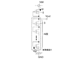
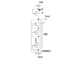
図1は、一実施例を説明するための回路図である。
本実施例の赤外線センサーは、断熱構造体1(図12参照。)上に形成されたセンサーMOSFET3と、断熱構造体1の外部に形成された電流源MOSFET5から構成される。センサーMOSFET3及び電流源MOSFET5は、サブスレッショルド領域で動作している同じ導電型のMOSFETであり、例えばN型のMOSFETで構成されている。
FIG. 1 is a circuit diagram for explaining an embodiment.
The infrared sensor of the present embodiment includes a
センサーMOSFET3はゲートとドレインが短絡されたダイオード接続となっている。電流源MOSFET5はゲートとソースが短絡されている。電流源MOSFET5は、ゲートとソースが短絡されていることで、特別なバイアス電圧を必要とせずに、安定した定電流源を作ることが可能である。
上記のように結線されたセンサーMOSFET3と電流源MOSFET5は、電源VddとグランドGNDの間に直列に接続されている。センサーMOSFET3と電流源MOSFET5の接続ノードの電圧がセンサー出力電圧Voutとして用いられる。
The
The
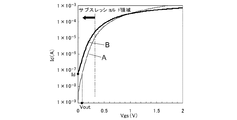
図2は、MOSFETのVgs−Id特性を示す図であり、波形Aはしきい値電圧がVthaのMOSFETをダイオード接続した場合のVgs−Id特性を示し、波形Bはしきい値電圧がVthbのMOSFETの一定Vds(ソース−ドレイン間電圧)時のVgs−Id特性を示す。また、図2中の一点鎖線の左側の領域がおおよそのサブスレッショルド領域である。 FIG. 2 is a diagram showing the Vgs-Id characteristics of a MOSFET. A waveform A shows a Vgs-Id characteristic when a MOSFET having a threshold voltage of Vtha is diode-connected, and a waveform B shows a threshold voltage of Vthb. The Vgs-Id characteristic at the time of constant Vds (source-drain voltage) of MOSFET is shown. In addition, a region on the left side of the alternate long and short dash line in FIG. 2 is an approximate subthreshold region.
例えば、図1のセンサーMOSFET3を図2の波形Aの特性とし、図1の電流源MOSFET5を図2の波形Bの特性とすれば、波形BのVgs=0の点が電流源電流Idとなり、電流源電流Idと波形Aの特性から決まる電圧がセンサー出力電圧Voutとなる。このとき、センサー出力電圧VoutはMOSFET3,5のしきい値電圧差ΔVthとほぼ等しくなる。
For example, if the
また、後述する多段接続構成においては、低電圧動作を可能とするために図1のセンサー出力電圧Vout、つまりしきい値電圧差ΔVthを小さくする必要がある。例えば、センサー出力電圧Vout≒しきい値電圧差ΔVth=50mVを出力させる場合、図1のMOSFET3,5を飽和領域で動作させると、センサーMOSFET3と電流源MOSFET5で互いにVdsが異なるため、このVds差によってセンサー出力電圧Vout>しきい値電圧差ΔVthとなり、目的とする微小なしきい値電圧差ΔVthを出力することができない。
Further, in the multistage connection configuration described later, it is necessary to reduce the sensor output voltage Vout of FIG. 1, that is, the threshold voltage difference ΔVth in order to enable low voltage operation. For example, when outputting the sensor output voltage Vout≈threshold voltage difference ΔVth = 50 mV, if the
本発明においては、図1のセンサーMOSFET3と電流源MOSFET5を共にサブスレッショルド領域で動作させることにより、微小なセンサー出力電圧Vout≒しきい値電圧差ΔVthを出力することが可能である。これは、サブスレッショルド領域でMOSFETに流れる電流は、ソース−ドレイン間電圧Vdsにほとんど依存しないためである。
In the present invention, it is possible to output a minute sensor output voltage Vout≈threshold voltage difference ΔVth by operating both the
また、本発明のセンサーにおいては、同一ゲートバイアス(同一Vgs)時のセンサーMOSFET3のサブスレッショルド領域電流が電流源MOSFET5のサブスレッショルド領域電流以下となるように設計されなければならない。このように設計することにより、図1に示した構成のセンサーにおいて、微小なセンサー出力電圧Vout≒しきい値電圧差ΔVthを出力することが可能である。
The sensor of the present invention must be designed so that the subthreshold region current of the
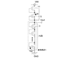
図3は、他の実施例を説明するための回路図である。
この実施例では、センサーMOSFET3がN段直列に接続されている。図1で示した1段構成の場合と同様に、N段のセンサーMOSFET3は全て断熱構造体1上に形成されている。この実施例のように、センサーMOSFET3をN段に接続することによって、赤外線センサーの感度をN倍にすることが可能である。
FIG. 3 is a circuit diagram for explaining another embodiment.
In this embodiment, the
また、このとき、センサー出力電圧VoutのDCレベルも1段の場合と比較してN倍となるため、センサーMOSFET31段あたりのVgsを小さくする必要がある。前述のように、センサーMOSFET3及び電流源MOSFET5をサブスレッショルド領域で動作させ、センサーMOSFET3のしきい値電圧と電流源MOSFET5のしきい値電圧の差ΔVthを小さくすることにより、MOSFET31段あたりのVgs(図1におけるVout)を小さくすることが可能となる。
At this time, since the DC level of the sensor output voltage Vout is also N times that in the case of one stage, it is necessary to reduce Vgs per 31 stages of the sensor MOSFET. As described above, the
例えば、MOSFET31段あたりのVgsが50mV、直列の段数が50段の場合、図3のVoutは2.5Vとなり、電源電圧3Vで駆動が可能である。このとき、感度はMOSFET31段の場合と比較して、50倍となる。 For example, when the Vgs per 31 stages of MOSFET is 50 mV and the number of series stages is 50, Vout in FIG. 3 is 2.5 V, which can be driven with a power supply voltage of 3 V. At this time, the sensitivity is 50 times that of the case of 31 MOSFETs.
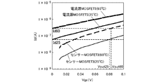
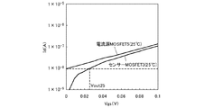
図4は、センサーMOSFETのId−Vgs特性の一例を示す図である。
図11に示した従来の赤外線センサーにおいて、電流源103が温度依存性を持たないように設計されている場合、電流Idは周囲温度に依存せずに一定となる。一方で、センサーMOSFET101は周囲温度が25℃と60℃の場合で、図4のように特性が変化する。周囲温度25℃の場合、センサー出力電圧Vout25は約0.096Vであるのに対し、周囲温度が60℃の場合にはセンサー出力電圧Vout60は約0.044Vとなり、約0.052Vの変化が生じている。これは、図11で示したような1段構成の場合はわずかな変化量であるが、図3で示したような多段構成の場合は影響が大きくなる。例えば、多段構成でN=50段とすると、周囲温度が25℃の場合、センサー出力電圧Voutは約4.8Vとなり、60℃の場合、センサー出力電圧Voutは約2.2Vまで低下する。
FIG. 4 is a diagram illustrating an example of the Id-Vgs characteristics of the sensor MOSFET.
In the conventional infrared sensor shown in FIG. 11, when the
また、周囲温度が低くなれば、反対にセンサー出力電圧Voutは4.8Vより高くなる方向へとシフトする。また、赤外線センサーの使用温度範囲を0〜80℃とすればセンサー出力電圧Voutの変化幅は5V近くになる。また、赤外線センサーの感度向上のために、センサーMOSFET3の温度係数を高く設計すれば、周囲温度の変化によるセンサー出力電圧Voutの変化量はさらに大きくなる。
上述のように、従来技術は、このような周囲温度の変化によるVoutの変化を抑制するために、ペルチェ素子等の冷却素子を用いてセンサーMOSFETの温度を常に一定になるように制御していた。
On the other hand, if the ambient temperature is lowered, the sensor output voltage Vout is shifted to a direction higher than 4.8V. Further, if the operating temperature range of the infrared sensor is 0 to 80 ° C., the change width of the sensor output voltage Vout becomes close to 5V. In addition, if the temperature coefficient of the
As described above, the prior art has controlled the temperature of the sensor MOSFET to be always constant by using a cooling element such as a Peltier element in order to suppress such a change in Vout due to a change in ambient temperature. .
図5は、図1に示した赤外線センサーを構成するセンサーMOSFET3と電流源MOSFET5のId−Vgs特性の一例を示す図である。
周囲温度25℃の場合、電流源MOSFET5が流す電流Id25とセンサーMOSFET3の特性との関係から出力電圧Vout25は約0.080Vである。周囲温度60℃の場合、電流源MOSFET5が流す電流Id60とセンサーMOSFET3の特性との関係から出力電圧Vout2は約0.082Vである。このように、周囲温度が25〜60℃の場合に、センサー出力電圧Voutの変化量は約0.002Vとなり、図11及び図4を参照して説明した従来のセンサーと比較すると、センサー出力電圧Voutの変化量は約1/26に抑制されている。
FIG. 5 is a diagram showing an example of the Id-Vgs characteristics of the
When the ambient temperature is 25 ° C., the output voltage Vout25 is about 0.080 V from the relationship between the current Id25 flowing through the
また、図3に示した多段構成でN=50段の場合を考えると、周囲温度が25℃のときはセンサー出力電圧Voutは約4.0V、周囲温度60℃のときはセンサー出力電圧Voutは約4.1Vとなり、周囲温度変化に対してセンサー出力電圧VoutのDCレベル変化が小さく多段構成の赤外線センサーを実現できる。 Considering the case of N = 50 stages in the multistage configuration shown in FIG. 3, when the ambient temperature is 25 ° C., the sensor output voltage Vout is about 4.0 V, and when the ambient temperature is 60 ° C., the sensor output voltage Vout is Since the voltage level is about 4.1 V, the DC level change of the sensor output voltage Vout is small with respect to the ambient temperature change, so that a multistage infrared sensor can be realized.
本発明の特徴は、センサーMOSFET3と電流源MOSFET5を同じ導電型のMOSFETで構成し、ともにサブスレッショルド領域で動作させることにより、センサーMOSFET3と電流源MOSFET5がほとんど同じ温度特性を持つようにしたことである。これにより、周囲温度が変化した場合においても、ペルチェ素子等の冷却素子を使用することなく、センサー出力電圧Voutをほぼ一定に保つことが可能となる。また、センサー出力電圧Voutの変化が抑制されることにより、電源電圧を低く設定することができ、低電圧動作、低消費電力動作が可能となる。
The feature of the present invention is that the
ところで、周囲温度の変化によるセンサー出力電圧Voutの変化をさらに精度良く抑制するためには、よりセンサーMOSFET3と電流源MOSFET5の温度特性を合わせることが好ましい。このためには、センサーMOSFET3と電流源MOSFET5を同じ導電型のMOSFETで構成することに加えて、構造も同じにする方法がある。つまり、センサーMOSFET3と電流源MOSFET5のサイズ(ゲート長、ゲート幅)を同じにすることにより、センサーMOSFET3と電流源MOSFET5の温度特性がより近くなり、周囲温度の変化によるセンサー出力電圧Voutの変化をさらに精度良く抑制することが可能となる。
By the way, in order to suppress the change of the sensor output voltage Vout due to the change of the ambient temperature with higher accuracy, it is preferable to match the temperature characteristics of the
また、周囲温度の変化によるセンサー出力電圧Voutの変化をさらに精度良く抑制するためには、センサーMOSFET3と電流源MOSFET5のチャネル不純物濃度とプロファイルを同じにする方法がある。つまり、センサーMOSFET3と電流源MOSFET5は、導電型、構造、しきい値電圧が等しい、全く同じ構造のMOSFETで構成される(このような条件の二つのトランジスタをペアトランジスタと呼ぶ)。ただし、結線は図1又は図3に示した状態にする。
In order to suppress the change in the sensor output voltage Vout due to the change in the ambient temperature with higher accuracy, there is a method in which the channel impurity concentrations and profiles of the
図6は図1に示した赤外線センサーを構成するセンサーMOSFET3と電流源MOSFET5をペアトランジスタで構成した場合のセンサーMOSFET3と電流源MOSFET5のId−Vgs特性の一例を示す図である。
FIG. 6 is a diagram showing an example of Id-Vgs characteristics of the
図6に示すように、センサーMOSFET3と電流源MOSFET5を全く同じ構造のペアトランジスタで構成した場合、結線の違いによってセンサー出力電圧Vout25は約25mVという非常に小さな電圧が出力される。このことから、図3に示した多段構成にすることが非常に容易となる。
また、センサーMOSFET3と電流源MOSFET5は全く同じ構造のMOSFETであるため、プロセスばらつきの少ない非常に安定したセンサー出力電圧Voutを作り出すことが可能である。
As shown in FIG. 6, when the
Further, since the
前記のように、センサーMOSFET3と電流源MOSFET5を全く同じ構造のペアトランジスタで構成すれば容易に安定したセンサー出力電圧Voutを作り出すことができるが、センサーMOSFET3と電流源MOSFET5がペアトランジスタでない構成においても本発明のセンサーを実現可能である。例えば、センサーMOSFET3と電流源MOSFET5はチャネル不純物濃度以外は同一構造のトランジスタであってもよい。また、センサーMOSFET3と電流源MOSFET5はゲート不純物濃度以外は同一構造のトランジスタであるようにしてもよい。ただし、センサーMOSFET3と電流源MOSFET5でゲート−ソース間電圧が同一である場合にセンサーMOSFET3のサブスレッショルド領域電流が電流源MOSFET5のサブスレッショルド領域電流以下になるように設定される。
As described above, if the
チャネル不純物濃度やゲート不純物濃度が互いに異なる2つのMOSFETは、しきい値電圧も互いに異なる。すなわち、センサーMOSFET3と電流源MOSFET5で、チャネル不純物濃度やゲート不純物濃度を互いに異ならせることにより、センサーMOSFET3と電流源MOSFET5のしきい値電圧差ΔVthを所望の値に制御することができ、より小さなしきい値電圧差ΔVthを得ることができる。これにより、センサーMOSFET3をさらに多段にして高感度の赤外線センサーを形成することができる。また、センサーMOSFETのしきい値電圧によってセンサーMOSFETの温度感度が異なるので、センサーMOSFETのしきい値電圧を温度感度が高くなる値へ調整することによって高感度の赤外線センサーを形成することができる。
Two MOSFETs having different channel impurity concentrations and different gate impurity concentrations also have different threshold voltages. That is, by making the channel impurity concentration and the gate impurity concentration different between the
ここまで、センサーMOSFET3と電流源MOSFET5はN型のMOSFETの構成で説明してきたが、センサーMOSFETと電流源MOSFETをP型のMOSFETで構成してもよい。
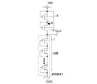
図7は、さらに他の実施例を説明するための回路図である。
この実施例は断熱構造体1上に形成されたN段のセンサーMOSFET7と、断熱構造体1の外部に形成された電流源MOSFET9から構成される。センサーMOSFET7及び電流源MOSFET9は、サブスレッショルド領域で動作しているP型のMOSFETで構成されている。
Up to this point, the
FIG. 7 is a circuit diagram for explaining still another embodiment.
This embodiment includes an N-
各センサーMOSFET7はゲートとドレインが短絡されたダイオード接続となっている。電流源MOSFET9はゲートとソースが短絡されている。センサーMOSFET7と電流源MOSFET9の接続ノードの電圧がセンサー出力電圧Voutとして用いられる。
この実施例でも、図3に示したN型のセンサーMOSFET3及び電流源MOSFET5を備えたセンサーと同様の作用及び効果を得ることができる。
この実施例はN段のセンサーMOSFET7を備えているが、センサーMOSFET7は1段であってもよい。
Each
Also in this embodiment, the same operation and effect as the sensor including the N-
Although this embodiment includes an N-
図8は、さらに他の実施例を説明するための回路図である。
この実施例では、定電流源が電流源MOSFET5と第2電流源MOSFET11の二つのMOSFETで構成されている。第2電流源MOSFET11は電源電圧Vddの変化による電流Idの変化を抑制するためのものである。第2電流源MOSFET11は、電源Vddと電流源MOSFET5の間に直列に接続され、ゲートとソースが短絡され、バックゲートはセンサー出力電圧Voutに接続されている。
FIG. 8 is a circuit diagram for explaining still another embodiment.
In this embodiment, the constant current source is composed of two MOSFETs, a
このように第2電流源MOSFET11を接続することにより、電源電圧Vddの変化により電流Idが変化しても、センサー出力電圧Voutの変化として第2電流源MOSFET11のバックゲートへとフィードバックが掛かり、電流Idの変化が抑制される。第2電流源MOSFET11は、電流源MOSFET5と全く同じ構成のMOSFETとするか、第2電流源MOSFET11で電流Idが制限されてしまわないように電流源MOSFET5よりも電流が多く流れるように設計されている。
By connecting the second
図9は、さらに他の実施例を説明するための回路図である。
この実施例は、P型MOSFETで構成された図7のセンサーに対して、P型の第3電流源MOSFET13をさらに備えている。第3電流源MOSFET13は、センサーMOSFET7と電流源MOSFET9の間に直列に接続され、ゲートとソースが短絡され、バックゲートは電源Vddに接続されている。
FIG. 9 is a circuit diagram for explaining still another embodiment.
In this embodiment, a P-type third
このように第3電流源MOSFET13を接続することにより、電源電圧Vddが変化しても、Voutと第3電流源MOSFET13のバックゲート間電圧へとフィードバックが掛かり、電流Idの変化が抑制される。第3電流源MOSFET13は、電流源MOSFET9と全く同じ構成のMOSFETとするか、電流源MOSFET11で電流Idが制限されてしまわないように電流源MOSFET5よりも電流が多く流れるように設計されている。
By connecting the third
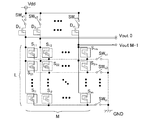
図10は、さらに他の実施例を説明するための回路図であり、本発明を適用した赤外線アレイセンサーの一例を示した図である。
アレイセンサーはL×M個の画素S11〜Slm、定電流源D1〜Dm、列選択スイッチSWa1〜SWam、行選択スイッチSWb1〜SWblから構成されており、出力センサー出力電圧Vout0〜センサー出力電圧VoutM−1が出力される。なお、L=1のラインセンサーの場合には、行選択スイッチ、列選択スイッチは不要である。
FIG. 10 is a circuit diagram for explaining still another embodiment, and is a diagram showing an example of an infrared array sensor to which the present invention is applied.
The array sensor includes L × M pixels S11 to Slm, constant current sources D1 to Dm, column selection switches SWa1 to SWam, and row selection switches SWb1 to SWbl. The output sensor output voltage Vout0 to the sensor output voltage VoutM−. 1 is output. In the case of a line sensor with L = 1, a row selection switch and a column selection switch are not necessary.
各画素S11〜Slmは、上記の実施例で説明したように、断熱構造体とセンサーMOSFETから構成されている。図10では、各画素S11〜SlmでセンサーMOSFETが1段の構成を示しているが、各画素S11〜SlmにおいてセンサーMOSFETは多段であってもよい。例えば、断熱構造体上に形成できる数又は電源電圧で決まる数だけセンサーMOSFETを多段に接続した構成であってもよい。
定電流源は列の数、あるいは行の数だけ形成し、行選択スイッチ、列選択スイッチによって選択された画素に、定電流を供給する。各定電流源D1〜Dmは、電流源MOSFET一つからなる構成を示しているが、図8及び図9を参照して説明したように、電流源MOSFET2つからなる構成としてもよい。
Each pixel S11-Slm is comprised from the heat insulation structure and sensor MOSFET as demonstrated in said Example. In FIG. 10, each pixel S11 to Slm has a single-stage sensor MOSFET. However, each pixel S11 to Slm may have multiple stages of sensor MOSFETs. For example, a configuration in which sensor MOSFETs are connected in multiple stages by the number that can be formed on the heat insulating structure or the number determined by the power supply voltage may be used.
The constant current sources are formed by the number of columns or the number of rows, and supply a constant current to the pixels selected by the row selection switch and the column selection switch. Each of the constant current sources D1 to Dm is configured with one current source MOSFET, but may be configured with two current source MOSFETs as described with reference to FIGS.
各画素から得られたセンサー出力電圧Vout0〜VoutM−1は順次アンプ等の後段回路に送られる。
このような赤外線アレイセンサーでは、特に小型化や低消費電力化が望まれているため、本発明を適用すれば、ペルチェ素子等の電気的な冷却素子が不要となり、低電圧動作も可能となることから、大幅なシステムの小型化、簡易化、低コスト化、低消費電力化が可能となる。
Sensor output voltages Vout0 to VoutM-1 obtained from each pixel are sequentially sent to a subsequent circuit such as an amplifier.
In such an infrared array sensor, since downsizing and low power consumption are particularly desired, if the present invention is applied, an electric cooling element such as a Peltier element becomes unnecessary, and a low voltage operation is also possible. As a result, the system can be greatly reduced in size, simplified, reduced in cost, and reduced in power consumption.
以上、本発明の実施例を説明したが、上記実施例における回路構成等は一例であり、本発明はこれらに限定されるものではなく、特許請求の範囲に記載された本発明の範囲内で種々の変更が可能である。
例えば、上記実施例では、電流源MOSFET5,9,11,13はゲートとソースが短絡されているが、本発明はこれに限定されるものではなく、電流源MOSFETのゲートに所定の電圧を印加して電流源MOSFETを動作させてもよい。
また、上記実施例では、センサーMOSFETを構成するMOSFET3,7はゲートとドレインが短絡されているが、本発明はこれに限定されるものではなく、センサーMOSFETを構成するMOSFETのゲートに所定の電圧を印加してセンサーMOSFETを動作させてもよい。
As mentioned above, although the Example of this invention was described, the circuit structure in the said Example is an example, This invention is not limited to these, In the range of this invention described in the claim Various changes are possible.
For example, in the above embodiment, the gates and sources of the
In the above embodiment, the gates and drains of the
本発明は、例えば生体検知センサーや赤外線カメラ等、赤外線を受光又は放出することで発生する熱によって特性が変化する赤外線センサーを備えた機器に応用される。 The present invention is applied to a device including an infrared sensor whose characteristics change due to heat generated by receiving or emitting infrared rays, such as a living body detection sensor and an infrared camera.
1 断熱構造体
3 N型のセンサーMOSFET
5 N型の電流源MOSFET
7 P型のセンサーMOSFET
9 P型の電流源MOSFET
11 第2電流源MOSFET
13 第3電流源MOSFET
1 Thermal insulation structure 3 N-type sensor MOSFET
5 N-type current source MOSFET
7 P-type sensor MOSFET
9 P-type current source MOSFET
11 Second current source MOSFET
13 Third current source MOSFET
Claims (7)
前記センサーMOSFETと前記電流源MOSFETの間の端子がセンサー出力端子を構成し、
前記センサーMOSFETは断熱構造体上に配置され、
前記電流源MOSFETは前記断熱構造体の外部に配置されており、
前記センサーMOSFET及び前記電流源MOSFETは同じ導電型のMOSFETからなり、かつサブスレッショルド領域で動作され、
前記センサーMOSFETはゲートとドレインが短絡され、前記電流源MOSFETはゲートとソースが短絡されており、
前記センサーMOSFETと前記電流源MOSFETでゲート−ソース間電圧が同一である場合に前記センサーMOSFETのサブスレッショルド領域電流が前記電流源MOSFETのサブスレッショルド領域電流よりも小さくなるように設定されており、
前記センサーMOSFET及び前記電流源MOSFETはN型であり、
前記定電流源は、前記断熱構造体の外部に配置され、サブスレッショルド領域で前記電流源MOSFETが流す電流以上の電流を流すことができるN型の第2電流源MOSFETをさらに備え、
前記第2電流源MOSFETは、前記電流源MOSFETの電源側に直列に接続され、ゲートとソースが短絡され、かつバックゲートが前記センサー出力端子に接続されている赤外線センサー。 A sensor MOSFET and a current source MOSFET connected in series to the sensor MOSFET and constituting a constant current source for driving the sensor MOSFET with a constant current;
A terminal between the sensor MOSFET and the current source MOSFET constitutes a sensor output terminal,
The sensor MOSFET is disposed on a heat insulating structure,
The current source MOSFET is disposed outside the heat insulating structure,
The sensor MOSFET and the current source MOSFET are made of MOSFETs of the same conductivity type and are operated in a subthreshold region,
The sensor MOSFET has a gate and drain short-circuited, and the current source MOSFET has a gate and source short-circuited,
When the gate-source voltage is the same between the sensor MOSFET and the current source MOSFET, the subthreshold region current of the sensor MOSFET is set to be smaller than the subthreshold region current of the current source MOSFET,
The sensor MOSFET and the current source MOSFET are N-type,
The constant current source further includes an N-type second current source MOSFET that is disposed outside the heat insulating structure and can flow a current equal to or greater than a current that the current source MOSFET flows in a subthreshold region,
The second current source MOSFET is an infrared sensor connected in series to the power source side of the current source MOSFET, a gate and a source are short-circuited, and a back gate is connected to the sensor output terminal.
前記センサーMOSFETと前記電流源MOSFETの間の端子がセンサー出力端子を構成し、
前記センサーMOSFETは断熱構造体上に配置され、
前記電流源MOSFETは前記断熱構造体の外部に配置されており、
前記センサーMOSFET及び前記電流源MOSFETは同じ導電型のMOSFETからなり、かつサブスレッショルド領域で動作され、
前記センサーMOSFETはゲートとドレインが短絡され、前記電流源MOSFETはゲートとソースが短絡されており、
前記センサーMOSFETと前記電流源MOSFETでゲート−ソース間電圧が同一である場合に前記センサーMOSFETのサブスレッショルド領域電流が前記電流源MOSFETのサブスレッショルド領域電流よりも小さくなるように設定されており、
前記センサーMOSFET及び前記電流源MOSFETはP型であり、
前記定電流源は前記断熱構造体の外部に配置され、サブスレッショルド領域で前記電流源MOSFETが流す電流以上の電流を流すことができるP型の第3電流源MOSFETをさらに備え、
前記第3電流源MOSFETは、前記電流源MOSFETと前記センサーMOSFETの間に直列に接続され、ゲートとソースが短絡され、かつバックゲートが前記電流源MOSFETの電源側の端子に接続されている赤外線センサー。 A sensor MOSFET and a current source MOSFET connected in series to the sensor MOSFET and constituting a constant current source for driving the sensor MOSFET with a constant current;
A terminal between the sensor MOSFET and the current source MOSFET constitutes a sensor output terminal,
The sensor MOSFET is disposed on a heat insulating structure,
The current source MOSFET is disposed outside the heat insulating structure,
The sensor MOSFET and the current source MOSFET are made of MOSFETs of the same conductivity type and are operated in a subthreshold region,
The sensor MOSFET has a gate and drain short-circuited, and the current source MOSFET has a gate and source short-circuited,
When the gate-source voltage is the same between the sensor MOSFET and the current source MOSFET, the subthreshold region current of the sensor MOSFET is set to be smaller than the subthreshold region current of the current source MOSFET,
The sensor MOSFET and the current source MOSFET are P-type,
The constant current source further includes a P-type third current source MOSFET that is disposed outside the heat insulating structure and can flow a current equal to or greater than a current that the current source MOSFET flows in a subthreshold region,
The third current source MOSFET is connected in series between the current source MOSFET and the sensor MOSFET, a gate and a source are short-circuited, and a back gate is connected to a power supply side terminal of the current source MOSFET sensor.
画素選択を行なうための複数のスイッチを有し、
前記定電流源は、アレイ状に配置された前記センサーMOSFETに対して、同じ行又は列に配列された複数の前記センサーMOSFETごとに設けられていることを特徴とする赤外線アレイセンサー。 The infrared sensor according to any one of claims 1 to 6 is arranged in an array,
A plurality of switches for performing pixel selection;
An infrared array sensor, wherein the constant current source is provided for each of the plurality of sensor MOSFETs arranged in the same row or column with respect to the sensor MOSFETs arranged in an array.
Priority Applications (2)
| Application Number | Priority Date | Filing Date | Title |
|---|---|---|---|
| JP2011008163A JP5834412B2 (en) | 2011-01-18 | 2011-01-18 | Infrared sensor and infrared array sensor |
| US13/350,875 US8759772B2 (en) | 2011-01-18 | 2012-01-16 | Infrared sensor and infrared array sensor |
Applications Claiming Priority (1)
| Application Number | Priority Date | Filing Date | Title |
|---|---|---|---|
| JP2011008163A JP5834412B2 (en) | 2011-01-18 | 2011-01-18 | Infrared sensor and infrared array sensor |
Publications (2)
| Publication Number | Publication Date |
|---|---|
| JP2012149964A JP2012149964A (en) | 2012-08-09 |
| JP5834412B2 true JP5834412B2 (en) | 2015-12-24 |
Family
ID=46490066
Family Applications (1)
| Application Number | Title | Priority Date | Filing Date |
|---|---|---|---|
| JP2011008163A Expired - Fee Related JP5834412B2 (en) | 2011-01-18 | 2011-01-18 | Infrared sensor and infrared array sensor |
Country Status (2)
| Country | Link |
|---|---|
| US (1) | US8759772B2 (en) |
| JP (1) | JP5834412B2 (en) |
Families Citing this family (14)
| Publication number | Priority date | Publication date | Assignee | Title |
|---|---|---|---|---|
| US9360373B2 (en) | 2013-03-12 | 2016-06-07 | Ricoh Company, Ltd. | Infrared sensor of rear surface irradiation type |
| JP6263914B2 (en) | 2013-09-10 | 2018-01-24 | 株式会社リコー | Imaging device, driving method of imaging device, and camera |
| JP6225582B2 (en) | 2013-09-13 | 2017-11-08 | 株式会社リコー | Thermal infrared sensor |
| JP6387743B2 (en) | 2013-12-16 | 2018-09-12 | 株式会社リコー | Semiconductor device and manufacturing method of semiconductor device |
| JP6281297B2 (en) | 2014-01-27 | 2018-02-21 | 株式会社リコー | Phototransistor and semiconductor device |
| JP6354221B2 (en) | 2014-03-12 | 2018-07-11 | 株式会社リコー | Imaging apparatus and electronic apparatus |
| JP2016025261A (en) | 2014-07-23 | 2016-02-08 | 株式会社リコー | Imaging device, imaging device control method, and pixel structure |
| JP2016092178A (en) | 2014-11-04 | 2016-05-23 | 株式会社リコー | Solid state imaging device |
| US9985071B2 (en) * | 2016-04-15 | 2018-05-29 | Qualcomm Incorporated | Active area selection for LIDAR receivers |
| JP7289851B2 (en) * | 2018-04-17 | 2023-06-12 | オブシディアン センサーズ インコーポレイテッド | Readout circuit and method |
| JP7024624B2 (en) | 2018-06-25 | 2022-02-24 | 株式会社リコー | Support frame, spectroscope, spectroscopic analysis unit, and image forming apparatus |
| FR3086405B1 (en) * | 2018-09-24 | 2020-12-25 | St Microelectronics Sa | ELECTRONIC DEVICE CAPABLE OF FORMING A TEMPERATURE SENSOR OR A CURRENT SOURCE DELIVERING A CURRENT INDEPENDENT OF THE TEMPERATURE. |
| US11867570B2 (en) | 2020-03-06 | 2024-01-09 | Stmicroelectronics Sa | Thermal sensor circuit |
| CN120051670A (en) * | 2022-10-25 | 2025-05-27 | 松下知识产权经营株式会社 | Infrared sensor |
Family Cites Families (4)
| Publication number | Priority date | Publication date | Assignee | Title |
|---|---|---|---|---|
| JP2002296121A (en) | 2001-04-02 | 2002-10-09 | Mitsuteru Kimura | Temperature measuring device |
| AU2002345905A1 (en) * | 2001-06-22 | 2003-01-08 | Peregrine Semiconductor Corporation | Integrated photodetector for vcsel feedback control |
| JP2006258562A (en) | 2005-03-16 | 2006-09-28 | Hokkaido Univ | Far infrared sensor |
| JP2007101213A (en) | 2005-09-30 | 2007-04-19 | Ricoh Co Ltd | Semiconductor device, infrared sensor, and method of manufacturing semiconductor device |
-
2011
- 2011-01-18 JP JP2011008163A patent/JP5834412B2/en not_active Expired - Fee Related
-
2012
- 2012-01-16 US US13/350,875 patent/US8759772B2/en not_active Expired - Fee Related
Also Published As
| Publication number | Publication date |
|---|---|
| US20120181430A1 (en) | 2012-07-19 |
| JP2012149964A (en) | 2012-08-09 |
| US8759772B2 (en) | 2014-06-24 |
Similar Documents
| Publication | Publication Date | Title |
|---|---|---|
| JP5834412B2 (en) | Infrared sensor and infrared array sensor | |
| US10539470B2 (en) | Sub-threshold-based semiconductor temperature sensor | |
| JPH11272345A (en) | Reference voltage generation circuit | |
| US8552357B2 (en) | Photoelectric conversion apparatus | |
| US9035252B2 (en) | Detection circuit, sensor device, and electronic apparatus | |
| US20170170090A1 (en) | Power mos transistor die with temperature sensing function and integrated circuit | |
| US8581199B2 (en) | Solid state imaging device | |
| JP5339747B2 (en) | Infrared solid-state imaging device | |
| JP5517411B2 (en) | Infrared sensor and infrared solid-state imaging device | |
| JP2004165911A (en) | Driving method of transistor | |
| JP5121587B2 (en) | Reference voltage circuit | |
| US8692589B2 (en) | Semiconductor element driving circuit and semiconductor device | |
| US9000751B2 (en) | Voltage detecting circuit | |
| US9007049B2 (en) | Current source circuit with temperature compensation | |
| JP2003177828A (en) | Constant current circuit | |
| US20130154604A1 (en) | Reference current generation circuit and reference voltage generation circuit | |
| US8416021B2 (en) | Amplifier circuit | |
| US20150015326A1 (en) | Bulk-modulated current source | |
| CN121620213B (en) | Power device assembly with temperature sensing function | |
| JP7120463B2 (en) | Infrared detection element | |
| US7190205B2 (en) | Variable resistance circuit | |
| JP4524407B2 (en) | Semiconductor device | |
| JP4543193B2 (en) | Semiconductor device | |
| WO2011033663A1 (en) | Infrared imaging element | |
| JP5738954B2 (en) | Solid-state image sensor |
Legal Events
| Date | Code | Title | Description |
|---|---|---|---|
| A621 | Written request for application examination |
Free format text: JAPANESE INTERMEDIATE CODE: A621 Effective date: 20131202 |
|
| A977 | Report on retrieval |
Free format text: JAPANESE INTERMEDIATE CODE: A971007 Effective date: 20140820 |
|
| A131 | Notification of reasons for refusal |
Free format text: JAPANESE INTERMEDIATE CODE: A131 Effective date: 20140930 |
|
| A521 | Request for written amendment filed |
Free format text: JAPANESE INTERMEDIATE CODE: A523 Effective date: 20141112 |
|
| A131 | Notification of reasons for refusal |
Free format text: JAPANESE INTERMEDIATE CODE: A131 Effective date: 20150414 |
|
| A521 | Request for written amendment filed |
Free format text: JAPANESE INTERMEDIATE CODE: A523 Effective date: 20150511 |
|
| RD01 | Notification of change of attorney |
Free format text: JAPANESE INTERMEDIATE CODE: A7421 Effective date: 20150522 |
|
| A521 | Request for written amendment filed |
Free format text: JAPANESE INTERMEDIATE CODE: A821 Effective date: 20150522 |
|
| TRDD | Decision of grant or rejection written | ||
| A01 | Written decision to grant a patent or to grant a registration (utility model) |
Free format text: JAPANESE INTERMEDIATE CODE: A01 Effective date: 20151006 |
|
| A61 | First payment of annual fees (during grant procedure) |
Free format text: JAPANESE INTERMEDIATE CODE: A61 Effective date: 20151019 |
|
| R151 | Written notification of patent or utility model registration |
Ref document number: 5834412 Country of ref document: JP Free format text: JAPANESE INTERMEDIATE CODE: R151 |
|
| LAPS | Cancellation because of no payment of annual fees |