JP5822457B2 - Power supply device and image forming apparatus - Google Patents
Power supply device and image forming apparatus Download PDFInfo
- Publication number
- JP5822457B2 JP5822457B2 JP2010259292A JP2010259292A JP5822457B2 JP 5822457 B2 JP5822457 B2 JP 5822457B2 JP 2010259292 A JP2010259292 A JP 2010259292A JP 2010259292 A JP2010259292 A JP 2010259292A JP 5822457 B2 JP5822457 B2 JP 5822457B2
- Authority
- JP
- Japan
- Prior art keywords
- switching unit
- transformer
- fet
- voltage
- secondary side
- Prior art date
- Legal status (The legal status is an assumption and is not a legal conclusion. Google has not performed a legal analysis and makes no representation as to the accuracy of the status listed.)
- Active
Links
Images


Description
本発明は、同期整流方式のスイッチング電源装置、その電源装置を搭載した画像形成装置に関する。 The present invention relates to a synchronous rectification switching power supply and an image forming apparatus equipped with the power supply.
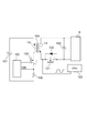
近年、電子機器装置の省電力化に伴い、電源装置の動作の効率化が要求されている。動作の効率化を実現した電源装置の一例として、特許文献1に記載の電源装置が提案されている。このような従来の電源装置の構成例を図8に示す。図8において、1は直流電源、2は主スイッチング素子としての電界効果トランジスタMOS−FET(以下、FETともいう)を制御する制御回路、4は主スイッチング素子としてのFET、5はトランスである。6は第2のスイッチング素子であるFET、7は平滑コンデンサ、8は電圧が供給される負荷、9は出力電圧検出回路、10はFET6に寄生するボディダイオード、11はFET6の駆動回路、12はFET6の電流検出回路である。
In recent years, with the power saving of electronic device apparatuses, there has been a demand for efficient operation of power supply apparatuses. As an example of a power supply device that achieves efficient operation, a power supply device described in Patent Document 1 has been proposed. A configuration example of such a conventional power supply apparatus is shown in FIG. In FIG. 8, 1 is a DC power source, 2 is a control circuit for controlling a field effect transistor MOS-FET (hereinafter also referred to as FET) as a main switching element, 4 is an FET as a main switching element, and 5 is a transformer. 6 is a FET as a second switching element, 7 is a smoothing capacitor, 8 is a load to which a voltage is supplied, 9 is an output voltage detection circuit, 10 is a body diode parasitic to
直流電源1からの入力電圧は、制御回路2および駆動回路3で制御されるFET4を導通する(オンする)ことでトランス5の1次巻線n1に励磁エネルギとして蓄積される。一方、FET4を非導通する(オフする)タイミングでトランス5の1次巻線n1に励磁されたエネルギは2次巻線n2に変換され、ボディダイオード10と電流検知回路12を通して負荷に供給される。電流検知回路12は電流が流れたことを検出すると駆動回路11にオン信号を送出し、FET6をオンする。また、電流検知回路12は自身に流れている電流が所定値以下になると電流が流れ終ったと判断し、今度は駆動回路12にオフ信号を送出してFET6をオフする。ボディダイオード10の順方向電圧による損失に対してFET6による損失は非常に低い。このため、ボディダイオード10に流れる電流をFET6側に切り替えるように制御することで、効率の向上を図っていた。このような方式は同期整流方式と呼ばれており、FET6は同期整流用のFETとも呼ばれる。
The input voltage from the DC power supply 1 is stored as excitation energy in the primary winding n1 of the
しかしながら、上記従来例では次のような課題があった。上記の同期整流方式の場合、動作の効率を向上するために同期整流用のFETのオンオフを検知する回路を設ける構成であり、この検知回路は複雑になる。従って、回路規模が大きくなり、コストアップを招いていた。また、二次巻線に流れる電流をカレントトランスで検知し、検知した電流によってFETのオンオフ制御を行う場合、軽負荷時では二次巻線に流れる電流量が僅かであり、カレントトランスから出力される電流も非常に小さくなってしまいFETのオンオフを正しく制御できない状態になる。FETのオンオフが正しく制御(駆動)されないと、効率の低下、また、消費電力が増大する可能性がある。このような軽負荷時(軽負荷状態)は、動作を待機しているスタンバイ状態や消費電力を低減する省エネモード(スリープモードともいう)を指し、所謂、電子機器におけるデフォルトの状態である。このデフォルトの状態は、電子装置において一日の中でかなりの時間を占める状態であり、FETのオンオフ動作による消費電力の増加や損失が電子機器のトータルの消費電力に大きく影響する。 However, the above conventional example has the following problems. In the case of the synchronous rectification method described above, a circuit for detecting on / off of the FET for synchronous rectification is provided in order to improve the operation efficiency, and this detection circuit becomes complicated. Therefore, the circuit scale is increased, resulting in an increase in cost. In addition, when the current flowing through the secondary winding is detected by a current transformer and the FET is turned on and off using the detected current, the amount of current flowing through the secondary winding is small at light loads and is output from the current transformer. The current that flows becomes very small, and the on / off state of the FET cannot be controlled correctly. If ON / OFF of the FET is not controlled (driven) correctly, efficiency may be reduced and power consumption may be increased. Such a light load (light load state) indicates a standby state waiting for operation or an energy saving mode for reducing power consumption (also referred to as a sleep mode), which is a so-called default state in an electronic device. This default state occupies a considerable amount of time during the day in the electronic device, and an increase or loss in power consumption due to the on / off operation of the FET greatly affects the total power consumption of the electronic device.
従って、本発明は、上記の点に鑑み、同期整流方式のスイッチング電源において、簡単な回路構成で回路規模を小さくし、かつ、負荷の状態によらず同期整流動作を正しく実行して消費電力を低減することを目的とする。 Therefore, in view of the above points, the present invention reduces the circuit scale with a simple circuit configuration in a synchronous rectification type switching power supply, and correctly executes the synchronous rectification operation regardless of the load state, thereby reducing the power consumption. The purpose is to reduce.
上記目的を達成するための本発明の電源装置は、一次側と二次側が絶縁されたトランスと、前記トランスの一次側に入力される直流電圧をスイッチングする第一のスイッチング部と、前記第一スイッチング部に流れる電流を検出し、検出した値が一定になるように前記第一スイッチング部のオン時間を制御し、前記トランスの二次側に発生する電圧に応じて前記第一スイッチング部のオフ時間を制御する第一制御部と、前記前記トランスの二次側に接続され、前記第一スイッチング部がオフしている期間にオンする第二スイッチング部とを備えた電源装置において、前記トランスの二次側に発生する電圧に応じて前記第二スイッチング部をオンし、前記トランスの二次側から出力される電圧を所定値にするために前記第二スイッチング部のオンする時間を一定時間に設定する第二制御部を有することを特徴とする。 In order to achieve the above object, a power supply apparatus according to the present invention includes a transformer having a primary side and a secondary side insulated , a first switching unit that switches a DC voltage input to the primary side of the transformer, and the first The current flowing through the switching unit is detected, the on-time of the first switching unit is controlled so that the detected value is constant, and the first switching unit is turned off according to the voltage generated on the secondary side of the transformer. A power supply device comprising: a first control unit that controls time; and a second switching unit that is connected to a secondary side of the transformer and is turned on during a period in which the first switching unit is off. The second switching unit is turned on according to the voltage generated on the secondary side, and the second switching unit is turned on in order to set the voltage output from the secondary side of the transformer to a predetermined value. And having a second control unit for setting a time for a predetermined time.
また、本発明の画像形成装置は、記録材に画像を形成するための画像形成部と、
前記画像形成部の動作を制御する制御部と、前記制御部に電圧を供給する電源と、を備え、前記電源は、一次側と二次側が絶縁されたトランスと、前記トランスの一次側に入力される直流電圧をスイッチングする第一のスイッチング部と、前記第一スイッチング部に流れる電流を検出し、検出した値が一定になるように前記第一スイッチング部のオン時間を制御し、前記トランスの二次側に発生する電圧に応じて前記第一スイッチング部のオフ時間を制御する第一制御部と、前記前記トランスの二次側に接続され、前記第一スイッチング部がオフしている期間にオンする第二スイッチング部と、前記トランスの二次側に発生する電圧に応じて前記第二スイッチング部をオンし、前記トランスの二次側から出力される電圧を所定値にするために前記第二スイッチング部のオンする時間を一定時間に設定する第二制御部を有することを特徴とする。
An image forming apparatus of the present invention includes an image forming unit for forming an image on a recording material,
A control unit that controls the operation of the image forming unit; and a power source that supplies a voltage to the control unit, the power source being input to a primary side of the transformer, and a transformer having an insulated primary side and a secondary side Detecting a current flowing through the first switching unit and a first switching unit that switches the DC voltage to be controlled, and controlling an on-time of the first switching unit so that the detected value becomes constant, A first control unit that controls an off time of the first switching unit according to a voltage generated on the secondary side, and a period that is connected to the secondary side of the transformer and the first switching unit is off. To turn on the second switching unit according to the voltage generated on the secondary side of the transformer and the second switching unit that is turned on, and to set the voltage output from the secondary side of the transformer to a predetermined value And having a second control unit for setting the time for turning on the serial second switching unit to a predetermined time.
以上説明したように、本発明によれば、簡単な回路構成で回路規模を小さくし、かつ、負荷の状態によらず同期整流動作を正しく実行して消費電力を低減することが可能になる。 As described above, according to the present invention, the circuit scale can be reduced with a simple circuit configuration, and the synchronous rectification operation can be correctly executed regardless of the load state to reduce the power consumption.
次に、上述した課題を解決するための本発明の具体的な構成について、以下に実施例に基づき説明する。なお、以下に示す実施例は一例であって、この発明の技術的範囲をそれらのみに限定する趣旨のものではない。 Next, specific configurations of the present invention for solving the above-described problems will be described based on examples. In addition, the Example shown below is an example, Comprising: It is not the meaning which limits the technical scope of this invention only to them.
実施例1について以下に説明する。
図1は本発明の実施例1に係る電源装置の回路図であり、図2はその動作波形の一部を示した図である。以下、図1と図2を基にして、本実施例1の詳細説明を行う。
Example 1 will be described below.
FIG. 1 is a circuit diagram of a power supply device according to Embodiment 1 of the present invention, and FIG. 2 is a diagram showing a part of its operation waveform. Hereinafter, the first embodiment will be described in detail with reference to FIGS. 1 and 2.
101は直流電圧電源であり、コンセント(商用電源)から供給されてダイオードブリッジ(不図示)で全波整流されたAC電圧をコンデンサ(不図示)で平滑することで直流電圧が得られる。102は制御部としての制御ICであり、第一のスイッチング素子としてのMOS−FET103(以下、FETという)のオンオフ動作を制御する。104は一次側と二次側の絶縁を取りつつ一次側のエネルギを二次側に変換するトランスであり、一次巻線のインダクタンスをLp、二次巻線のインダクタンスはLsである。105はFET103の電流を検知する電流検知用の抵抗、120は二次側の平滑コンデンサ、121は第二のスイッチング素子としてのMOS−FET(以下、FETという)であり、二次側の電圧を整流する同期整流用のFETである。122は同じく二次側電圧を整流するためのダイオード(ボディダイオードともいう)、123は電子機器の動作を制御する制御IC(CPU)である。なお、8は電圧が出力される負荷である。
電源装置が起動する際は、不図示の起動回路により制御IC102がFET103の駆動を開始する(オンする)。FET103がオンされるとトランス104の一次側、および、電流検知抵抗105に電流が流れるとともに、トランス104の一次巻き線に流れるピーク電流をIpとした場合、以下の式1で示されるエネルギE1が蓄積される。
E1=1/2Lp×Ip2 ・・・(式1)
このピーク電流Ipは電流検知抵抗によって電圧に変換され、制御IC102により一定値に制御される。このため入力電圧が変化してもトランス104に蓄積されるエネルギは略同じ値になる。例えば、100V系の電圧が入力される場合、入力電圧がAC85Vの時はピーク電流の傾きが立つ(単位時間あたりの変化量が大きい)ためFET103の駆動時間(オン時間ともいう)が短くなる。一方、入力電圧がAC140V時では電流の傾きが緩やかになる(単位時間あたりの変化量が小さい)ためFET103のオン時間は長くなる。このように入力電圧が異なっていても電流の流れている時間が異なるだけでピーク電流値は同じである。
When the power supply device is activated, the
E1 = 1/2 Lp × Ip 2 (Formula 1)
This peak current Ip is converted into a voltage by the current detection resistor, and is controlled to a constant value by the
一方、二次巻線に蓄積されるエネルギE2は、二次巻線に発生するピーク電流をIsとすると、以下の式2で示される。
E2=1/2Ls×Is2 ・・・(式2)
フライバック方式の電源の場合は、トランスの一次側で発生したエネルギと二次側に変換するエネルギが等しいため、トランス104の二次巻線に流れる電流は、入力電圧によらずに一定時間流れることになる。本実施例1においては、トランスの一次側の電流のピーク値に基づいて出力を制御する方式が前提となる。
On the other hand, the energy E2 accumulated in the secondary winding is expressed by the following equation 2 where Is is the peak current generated in the secondary winding.
E2 = 1 / 2Ls × Is 2 (Formula 2)
In the case of a flyback power supply, the energy generated on the primary side of the transformer is equal to the energy converted to the secondary side, so that the current flowing in the secondary winding of the
入力電圧が一定の場合、FET103のオン時間も一定であり、また、トランスの二次側の電流のオン時間も一定になる。そして、負荷8の状態の変化(負荷が大きい/小さい)に対応するため、オフ時間を変化させて周波数を可変する。つまり負荷の状態が変化したとしても、トランスの二次側に電流が流れている時間は一定となる。
When the input voltage is constant, the on time of the
図1の電源装置において、負荷8に対する出力電圧が大きい場合、例えば、24Vを出力している場合(重負荷時ともいう)は、二次側の電解コンデンサ120の出力側の電圧を検知してトランス104の一次側にフィードバックして、FET103の駆動を制御することに負荷に対して一定の電圧(24V)が出力するように制御される。なお、出力電圧が大きい場合とは、電子装置が動作を実行している状態であり、通常出力モードとも呼ばれる。
In the power supply device of FIG. 1, when the output voltage to the
一方、図2は、出力電圧が小さい場合、例えば、3.3Vを出力している場合(軽負荷時ともいう)の動作波形を示している。図2において、201はFET103に流れる電流波形、202はFET103のドレイン−ソース間の電圧波形、203はトランスの二次側の電流波形、204は同期整流用のFET121のドレイン−ソース間の電圧波形を示したものである。このように、FET121のドレイン−ソース間の電圧の立ち下がりとトランスの二次側の電流の流れ始めは同じタイミングになる。この立ち下りのタイミングを制御IC123で検出して、IC123がFET121ゲート端子をハイレベルにしてFET121を駆動する(オンする)。
On the other hand, FIG. 2 shows an operation waveform when the output voltage is small, for example, when 3.3 V is output (also referred to as a light load). In FIG. 2, 201 is a current waveform flowing through the
具体的には、ダイオード122のカソード端子に入力される電圧をIC123で検知して、その電圧の立下りタイミングを検知して、検知したタイミングでFET121を駆動するように制御する。
Specifically, the voltage input to the cathode terminal of the
また、FET121をオフするタイミングについては、本実施例1の方式がピーク電流を固定する方式を前提としているため、前述したようにオフ時間も固定となり、この時間を制御IC123に予め記憶させておく。IC123に予め記憶した一定時間経過後(オフ時間経過後)、FET121のゲート端子をローレベルにしてFET121をオフする。このオフ時間は予め設定された一定時間であり、本実施例では4μsに設定している。なお、このオフ時間は使用する回路や素子の特性に応じて適宜設定すればよい。
As for the timing of turning off the
なお、上記のIC123への電力は、トランス104の二次側からの電圧を降圧するDC/DCコンバータ(不図示)から供給されているものとする。
It is assumed that the power to the
また、出力電圧が小さい場合(軽負荷時)とは、電子装置が動作を実行せず、待機している状態であり、低電圧出力モードとも呼ばれる。 In addition, when the output voltage is small (when the load is light), the electronic device does not execute an operation and is on standby, and is also called a low voltage output mode.
以上、説明したように、同期整流方式の電源でトランスの一次側のピーク電流を固定する方式において、トランスの二次巻線の出力電圧の立ち下りを検出して、二次側の同期整流用FETの駆動を開始し、予め記憶した時間経過後に同期整流用のFETの駆動を停止するように制御する。これにより負荷の状態(大きさ)に関わらず安定して二次側の同期整流用のFETを正しく動作することができる。 As described above, in the method of fixing the peak current on the primary side of the transformer with the power supply of the synchronous rectification method, the falling of the output voltage of the secondary winding of the transformer is detected, and the synchronous rectification on the secondary side The driving of the FET is started, and the driving of the FET for synchronous rectification is controlled to stop after the prestored time has elapsed. As a result, the synchronous rectification FET on the secondary side can be operated correctly regardless of the state (size) of the load.
なお、本実施例1では二次側の整流用ダイオード122をFET121と個別に設ける構成したが、同期整流用のFETが備えるボディダイオードを利用することも可能である。
In the first embodiment, the secondary-
次に、実施例2について説明する。前述の実施例1では、トランスの一次側のピーク電流を固定する方式で、トランスの二次巻線の出力の立ち下りを検出して、二次側の同期整流用のFETの駆動を制御した。本実施例では、この実施例1の構成におけるトランスのインダクタンスのばらつきによる効率の低下を軽減する方式を提案する。 Next, Example 2 will be described. In the first embodiment, the transformer primary winding peak current is fixed, and the output of the secondary winding of the transformer is detected to control the driving of the secondary side synchronous rectification FET. . The present embodiment proposes a method for reducing the reduction in efficiency due to variations in transformer inductance in the configuration of the first embodiment.
実施例1で説明した構成では、例えば、トランスの一次側および二次側インダクタンスのばらつきや一次側の電流の検出回路である抵抗のばらつき等により、制御ICに記憶した時間と実際に二次側のFET121に電流が流れる時間に差が生じる可能性がある。特に、負荷がより大きい(重負荷ともいう)場合は、トランスの一次側に電流が流れ始めても、トランスの二次側のFET121を駆動し続けてしまう可能性がある。このような場合、一次側のFET6を再びオンする時、つまり、二次側巻線の巻き始め側に電圧が発生した時に、二次側のFET121が駆動し続けている状態になる。この状態では、二次側の電解コンデンサ120のマイナス側が逆方向にバイアスされて、二次側の電解コンデンサ120を劣化させる可能性がある。更には、電源の効率を低下させてしまう可能性もある。
In the configuration described in the first embodiment, for example, the time stored in the control IC and the actual secondary side due to variations in the primary and secondary inductances of the transformer, variations in resistance that is a primary-side current detection circuit, and the like. There is a possibility that a difference occurs in the time during which current flows in the
上記の記憶した時間と実際の時間に差が生じた時における、一次側の電流と二次側の電流の関係を図3に示す。301aは軽負荷時におけるトランスの一次側の電流,302bはトランスの二次側の電流を示しており、破線の区間がオフ時間となる。一方、302aが重負荷時におけるトランスの一次側の電流、302bが二次側の電流を示しており、二次側の電流がマイナス側に流れる期間(塗りつぶした三角形の領域)がトランスの一次側のFETと二次側のFETの駆動タイミングの重複期間である。この重複期間が生じると効率が低下する。なお同期整流方式ではなく、ダイオード整流方式であれば整流動作を終えた時点で自動的にオフするためこのような重複期間は略存在しない(ダイオードの逆回復時間は除く)。
FIG. 3 shows the relationship between the primary side current and the secondary side current when there is a difference between the stored time and the actual time.
本実施例では、上記のようにトランスの一次側のFETと二次側のFETの駆動タイミングが重複しないようにするために、負荷が大きい重負荷状態では同期整流動作を行わずにダイオード整流とし、オフ時間が十分に確保できる軽負荷状態で同期整流動作を行うように制御する。これにより、重負荷時における効率の低下を回避することができる。なお、オフ時間が十分に確保できている軽負荷の場合には、制御ICに記憶した時間と実際にトランスの二次側のFETを駆動する時間に多少の差が生じても、トランスの一次側のFETが再びオンするまでの時間に余裕があり、上記のような効率の低下に陥ることはない。 In this embodiment, in order to prevent the drive timing of the primary FET and secondary FET of the transformer from overlapping as described above, diode rectification is performed without performing synchronous rectification operation in a heavy load state where the load is large. Control is performed so that the synchronous rectification operation is performed in a light load state in which a sufficient off time can be secured. Thereby, the fall of the efficiency at the time of heavy load can be avoided. In the case of a light load with sufficient off-time, even if there is a slight difference between the time stored in the control IC and the time for actually driving the secondary side FET of the transformer, There is room in the time until the FET on the side is turned on again, and the above efficiency is not lowered.
なお、オフ時間が確保できる軽負荷状態とは、電子機器では動作を待機している待機状態(例えば、スタンバイ状態やスリープ状態(省電力状態)、実施例1で説明した出力電圧が3.3Vの状態)である。一方、電子機器が動作状態であれば軽負荷状態に比べて負荷が大きい重負荷状態(実施例1で説明した出力電圧が24Vの状態)になる。電子機器では待機状態の時間の方が、動作状態(稼動している状態)に比べて長いため、電子機器のトータル消費電力を低下するには、この待機状態における消費電力を低下することが重要である。 Note that the light load state in which the off time can be secured is a standby state in which the electronic device is waiting for operation (for example, a standby state or a sleep state (power saving state)), and the output voltage described in the first embodiment is 3.3V. State). On the other hand, if the electronic device is in an operating state, a heavy load state (a state in which the output voltage described in the first embodiment is 24 V) is greater than a light load state. In electronic devices, the standby time is longer than the operating state (operating state), so reducing the power consumption in this standby state is important to reduce the total power consumption of the electronic device. It is.
以下に、本実施例の動作について説明する。回路構成については実施例1(図1)の回路構成と略同様であるが、図4に示すように、二次側に整流用のダイオード124を追加している点が異なる。本実施例において実施例1と異なる動作は、トランスの二次側のFET121の駆動動作である。電子機器は、当然のことながら稼動状態のときに重負荷状態となり、機器が停止しているスタンバイ状態や機器の消費電力を下げたスリープ状態の時に軽負荷状態になる。本実施例では、電子機器の状態(モード)に応じてトランスの二次側のFETの動作を制御することを特徴とする。具体的には、重負荷状態においてはFET121を駆動させずに、ダイオード124によってダイオード整流動作に切り換える点が特徴である。
Hereinafter, the operation of this embodiment will be described. The circuit configuration is substantially the same as that of the first embodiment (FIG. 1) except that a rectifying
図5のフロチャートに基づき具体的な動作について説明する。まず、ステップ401において、電子機器が稼動状態であるか否かを検知する。例えば、電子機器が動作を開始したときを稼動状態、それ以外を非稼動状態と定義することができる。例えば、動作を開始したタイミングで、装置が稼動状態に入ったと判断すればよい。電子機器が稼動状態の場合(S401がYesの場合)、重負荷状態であると判断し、制御IC123は同期整流用のFET121の動作(制御)は行わず、整流動作はダイオード122で行うようにする。つまり、制御IC123はFET121を駆動しないようにする。FET121の駆動制御を行わない場合、トランスの二次側の電圧は自動的にダイオード124で整流されるように動作する。この場合は、トランスの一次側に電流が流れている期間、二次巻線の巻き始め側を正極とする電圧が発生するが、ダイオード124でブロックされるため、負荷8側に電流は流れない。そして、一次側の電流が流れ終わった時点で今度は二次巻線の巻き終わり側を正極とする電圧が発生し、負荷8(および電解コンデンサ120)からダイオード124→トランス104の二次巻線というルートで電流が流れる。この時はダイオード124の順方向と電流の方向が同一であるためダイオード124で電流がブロックされることはない。一方、ステップ401がNoの場合、つまり電子機器がスタンバイ状態、または、スリープ状態に遷移した場合は、ステップ402において二次巻線の出力の立ち下がりエッジが来るまで待機する。立ち下がりエッジを検出すると(S402がYesの場合)、ステップ403において、FET121のゲート端子をハイレベルにして、FET121をオンさせる。次にステップ404においてタイマをセットする。このとき設定するタイマ値は実施例1で説明したトランスに二次側に電流が流れている時間と同じ値かもしくは若干小さめの値とする。若干小さめに設定する理由は、仮に二次側に電流が流れる時間よりも実際流れる時間がばらつき等で大きくなった場合に、二次側の平滑コンデンサ120から電流を逆流させてしまう可能性があり、エネルギを無駄に浪費してしまう可能性があるからである。ステップ405では、タイマがゼロになるまで待機し、タイマがゼロになった時点で、ステップ406にてFET121のゲート端子をローレベルに設定し、FET121をオフさせる。
A specific operation will be described based on the flowchart of FIG. First, in step 401, it is detected whether or not the electronic device is in an operating state. For example, the time when the electronic device starts operating can be defined as an operating state, and the other time can be defined as a non-operating state. For example, it may be determined that the apparatus has entered the operating state at the timing when the operation is started. When the electronic device is in an operating state (when S401 is Yes), it is determined that the electronic device is in a heavy load state, and the
以上説明したように、電子機器が稼動状態である重負荷時は、同期整流方式ではなくダイオード整流方式とし、電子機器がスタンバイ状態、あるいは、スリープ状態の時に二次巻線の出力電圧の立ち下りを検出して同期整流用のFETの駆動を制御する。これにより、一次側のFETと二次側のFETの駆動タイミングが重複せずに駆動制御することができ、消費電力を抑えた同期整流動作が可能になる。 As explained above, the diode rectification method is used instead of the synchronous rectification method when the electronic device is operating, and the output voltage of the secondary winding falls when the electronic device is in the standby state or sleep state. Is detected to control the driving of the synchronous rectification FET. As a result, the drive control of the primary-side FET and the secondary-side FET can be controlled without overlapping, and a synchronous rectification operation with reduced power consumption becomes possible.
なお、スリープ状態における更なる低消費電力化を図るため、スリープ状態で出力電圧を下げる電源装置に適用する場合は。電源の切り替え信号を基にしてダイオード整流と同期整流の切り替えを行うことができる。 When applied to a power supply device that lowers the output voltage in the sleep state in order to further reduce power consumption in the sleep state. Switching between diode rectification and synchronous rectification can be performed based on a power supply switching signal.
次に実施例3について説明する。前述の実施例1、実施例2では、トランスの二次側のFETの駆動を電子機器の制御部(CPU)で制御していた。本実施例は、制御部ではなく駆動回路を用いて二次側のFETの駆動を制御する構成を特徴とする。 Next, Example 3 will be described. In the above-described first and second embodiments, the driving of the FET on the secondary side of the transformer is controlled by the control unit (CPU) of the electronic device. The present embodiment is characterized in that the drive of the secondary side FET is controlled using a drive circuit instead of the control unit.
以下、図6の回路図と図7の動作波形に基づき本実施例の構成について説明する。なお、図6において、実施例1(図1)と同じ構成要素については同一符号を付け、その説明は省略する。 The configuration of this embodiment will be described below based on the circuit diagram of FIG. 6 and the operation waveforms of FIG. In FIG. 6, the same components as those in the first embodiment (FIG. 1) are denoted by the same reference numerals, and the description thereof is omitted.
図6において、130は補助巻線であってトランスの二次側のFET121のゲート端子に電圧を供給するためのものである。C131はコンデンサであり、一端が補助巻線130の巻き終わり側に接続され、他端が二次側のFET121のゲート端子に接続されている。132は抵抗であり、一端が二次側のFET121のゲート端子に接続してあり、他端が補助巻線130の巻き始め側と二次側の出力のグランド側に接続してある。また、抵抗132と並列にダイオード133が、そのカソード側を二次側のFET121のゲート端子に接続されている。このような回路構成で、一次側のFET103がオフすると、補助巻線130の巻き終わり側を正極とする電圧が一定期間発生し、コンデンサ131を通して二次側のFET121のゲート端子に電圧が供給され始める。コンデンサ131と抵抗132は微分回路を形成しており、二次側のFET121に供給される電圧は徐々に減衰する。ダイオード133は二次側のFET121のゲート−ソース間の電圧が耐圧を超えないようにするために接続している。
6, 130 is an auxiliary winding for supplying a voltage to the gate terminal of the
図7はFET121のゲート端子に印加される電圧波形を示したものである。なお、縦軸は電圧値(V)示し、横軸は時間(t)を示している。電圧の減衰曲線が二次側のFET121のオン電圧であるVthを下回るタイミングが二次側のFET121のオン期間になる。このオン期間が所定値になるようにコンデンサ131と抵抗132の値を調整する。このようにオン期間を所定値にして同期整流動作が可能になる。
FIG. 7 shows a voltage waveform applied to the gate terminal of the
以上、説明したように、トランスに補助巻線を追加し、補助巻線の出力をコンデンサと抵抗による微分回路を通して二次側のFETのゲート端子に供給する。これにより、二次側のFETを一定時間オンすることができ、実施例1と同様に安定して正確な同期整流動作を実現することができる。 As described above, the auxiliary winding is added to the transformer, and the output of the auxiliary winding is supplied to the gate terminal of the secondary-side FET through the differentiation circuit using the capacitor and the resistor. As a result, the secondary FET can be turned on for a certain period of time, and a stable and accurate synchronous rectification operation can be realized as in the first embodiment.
なお、本実施例のようにハード的な回路を構成して同期整流用のFETを駆動制御した場合でも、実施例1や2と同様な動作を実現することが可能である。例えば、二次側のFETがオフするタイミングを二次側の電流がゼロになるタイミングよりも前(短く)設定し、二次側のFETのオフ直前でダイオード整流に切り替えるように制御すれば、各素子がばらついたとしても一次側のFETと二次側のFETの駆動タイミングを重複しないよう制御できる。 Even when the hardware circuit is configured and the synchronous rectification FET is driven and controlled as in the present embodiment, the same operation as in the first and second embodiments can be realized. For example, if the timing at which the secondary side FET is turned off is set before (shorter) than the timing at which the secondary side current becomes zero, and control is performed to switch to diode rectification immediately before the secondary side FET is turned off, Even if each element varies, the drive timing of the primary side FET and the secondary side FET can be controlled so as not to overlap.
また、実施例2の構成と同様に、整流用のダイオードを追加して、重負荷時においてダイオード整流に切り換える構成にすることも可能である。 Similarly to the configuration of the second embodiment, it is possible to add a rectifying diode and switch to diode rectification at heavy load.
<電源装置の適用例の説明>
次に、上記で説明した実施例1〜実施例3の電源装置を適用した装置の一例を図9に基づき説明する。上記の実施例1乃至実施例3で説明した電源装置を例えばレーザビームプリンタ、複写機、ファクシミリ等の画像形成装置における低電圧電源として適用することができる。画像形成装置における制御部としてのコントローラへの電力供給、また、用紙を搬送する搬送ローラの駆動部としてのモータへの電力供給のための電源として適用可能である。
<Description of application example of power supply device>
Next, an example of a device to which the power supply device according to the first to third embodiments described above is applied will be described with reference to FIG. The power supply apparatus described in the first to third embodiments can be applied as a low voltage power supply in an image forming apparatus such as a laser beam printer, a copying machine, or a facsimile. The present invention can be applied as a power source for supplying power to a controller as a control unit in an image forming apparatus and supplying power to a motor as a driving unit of a conveyance roller that conveys a sheet.
図9Aに画像形成装置の一例であるレーザビームプリンタの概略構成を示す。レーザビームプリンタ200は、画像形成部210として潜像が形成される像担持体としての感光ドラム211、感光ドラムに形成された潜像をトナーで現像する現像部212を備えている。そして感光ドラム211に現像されたトナー像をカセット216から供給された記録媒体としてのシート(不図示)に転写して、シートに転写したトナー像を定着器214で定着してトレイ215に排出する。また、図9Bに画像形成装置の制御部としてのコントローラと駆動部としてのモータへの電源からの電力供給ラインを示す。前述の電流共振電源は、このような画像形成動作を制御するCPU310有するコントローラへ300の電力供給、また、画像形成のための駆動部としてのモータ312、313に電力を供給する低圧電源として適用できる。供給する電力としては、コントローラ300へは3.3V、モータへは24Vを供給する。例えばモータ312はシートを搬送する搬送ローラを駆動するモータ、モータ313は定着器214を駆動するモータである。
FIG. 9A shows a schematic configuration of a laser beam printer which is an example of an image forming apparatus. The
このように画像形成装置の低電圧電源として適用した場合、画像形成動作を実行している状態の画像形成動作時は、モータに対して24Vを出力する状態であり、画像形成動作を実行せずに、動作を待機している省電力時は、コントローラに3.3Vを出力している状態である。 When applied as a low voltage power source for an image forming apparatus in this way, during the image forming operation in a state where the image forming operation is being executed, 24 V is output to the motor, and the image forming operation is not executed. In addition, during power saving while waiting for operation, 3.3V is being output to the controller.
なお、上記実施例1乃至3で説明した電源装置は、ここで説明した画像形成装置に限らず他の電子機器の低電圧電源としても適用可能である。 The power supply apparatus described in the first to third embodiments can be applied not only to the image forming apparatus described here but also as a low-voltage power supply for other electronic devices.
Claims (6)
前記トランスの二次側に発生する電圧に応じて前記第二スイッチング部をオンし、前記トランスの二次側から出力される電圧を所定値にするために前記第二スイッチング部のオンする時間を一定時間に設定する第二制御部
を有することを特徴とする電源装置。 A transformer primary side and the secondary side is insulated, a first switching unit for switching a DC voltage input to the primary side of the transformer to detect current flowing through the first switching unit, the detected value is constant A first control unit that controls the on-time of the first switching unit to control the off-time of the first switching unit according to the voltage generated on the secondary side of the transformer; In the power supply device including the second switching unit that is connected to the secondary side and is turned on during the period in which the first switching unit is turned off.
The second switching unit is turned on according to the voltage generated on the secondary side of the transformer, and the second switching unit is turned on in order to set the voltage output from the secondary side of the transformer to a predetermined value. A power supply apparatus comprising a second control unit for setting a predetermined time .
前記第二制御部は、前記第二スイッチング部がオンしてから前記一定時間経過したタイミングで前記第二スイッチング部をオフすることを特徴とする請求項1に記載の電源装置。2. The power supply device according to claim 1, wherein the second control unit turns off the second switching unit at a timing when the predetermined time has elapsed since the second switching unit was turned on.
前記第二制御部は、前記MOS−FETのドレイン端子とソース端子の間の電圧の立下りのタイミングに応じて前記第二スイッチング部をオンすることを特徴とする請求項1または2に記載の電源装置。 The second switching unit Ri MOS-FET der,
The said 2nd control part turns ON said 2nd switching part according to the timing of the fall of the voltage between the drain terminal of said MOS-FET, and a source terminal, The Claim 2 characterized by the above-mentioned. Power supply.
前記画像形成部の動作を制御する画像形成制御部と、
前記画像形成制御部に電圧を供給する電源と、を備え、
前記電源は、
一次側と二次側が絶縁されたトランスと、
前記トランスの一次側に入力される直流電圧をスイッチングする第一のスイッチング部と、
前記第一スイッチング部に流れる電流を検出し、検出した値が一定になるように前記第一スイッチング部のオン時間を制御し、前記トランスの二次側に発生する電圧に応じて前記第一スイッチング部のオフ時間を制御する第一制御部と、前記前記トランスの二次側に接続され、前記第一スイッチング部がオフしている期間にオンする第二スイッチング部と、前記トランスの二次側に発生する電圧に応じて前記第二スイッチング部をオンし、前記トランスの二次側から出力される電圧を所定値にするために前記第二スイッチング部のオンする時間を一定時間に設定する第二制御部
を有することを特徴とする画像形成装置。 An image forming unit for forming an image on a recording material;
An image forming control unit for controlling the operation of the image forming unit;
A power supply for supplying a voltage to the image formation control unit,
The power supply is
A transformer primary and secondary sides are insulated,
A first switching unit that switches a DC voltage input to a primary side of the transformer;
The first switching unit is detected according to the voltage generated on the secondary side of the transformer by detecting the current flowing through the first switching unit and controlling the on-time of the first switching unit so that the detected value is constant. A first control unit that controls an off time of the unit, a second switching unit that is connected to a secondary side of the transformer and that is turned on while the first switching unit is off, and a secondary side of the transformer The second switching unit is turned on in accordance with the voltage generated at the second, and the second switching unit is turned on for a predetermined time in order to set the voltage output from the secondary side of the transformer to a predetermined value . An image forming apparatus having two control units.
前記第二制御部は、前記第二スイッチング部がオンしてから前記一定時間経過したタイミングで前記第二スイッチング部をオフすることを特徴とする請求項4に記載の画像形成装置。The image forming apparatus according to claim 4, wherein the second control unit turns off the second switching unit at a timing when the predetermined time has elapsed since the second switching unit was turned on.
前記第二制御部は、前記MOS−FETのドレイン端子とソース端子の間の電圧の立下りのタイミングに応じて前記第二スイッチング部をオンすることを特徴とする請求項4または5に記載の画像形成装置。The said 2nd control part turns ON said 2nd switching part according to the fall timing of the voltage between the drain terminal of said MOS-FET, and a source terminal, The Claim 4 or 5 characterized by the above-mentioned. Image forming apparatus.
Priority Applications (3)
| Application Number | Priority Date | Filing Date | Title |
|---|---|---|---|
| JP2010259292A JP5822457B2 (en) | 2010-11-19 | 2010-11-19 | Power supply device and image forming apparatus |
| US12/969,283 US8472833B2 (en) | 2009-12-21 | 2010-12-15 | Power supply and image forming apparatus |
| CN201010597990.3A CN102104337B (en) | 2009-12-21 | 2010-12-15 | Power supply and image processing system |
Applications Claiming Priority (1)
| Application Number | Priority Date | Filing Date | Title |
|---|---|---|---|
| JP2010259292A JP5822457B2 (en) | 2010-11-19 | 2010-11-19 | Power supply device and image forming apparatus |
Publications (3)
| Publication Number | Publication Date |
|---|---|
| JP2012114978A JP2012114978A (en) | 2012-06-14 |
| JP2012114978A5 JP2012114978A5 (en) | 2014-01-09 |
| JP5822457B2 true JP5822457B2 (en) | 2015-11-24 |
Family
ID=46498576
Family Applications (1)
| Application Number | Title | Priority Date | Filing Date |
|---|---|---|---|
| JP2010259292A Active JP5822457B2 (en) | 2009-12-21 | 2010-11-19 | Power supply device and image forming apparatus |
Country Status (1)
| Country | Link |
|---|---|
| JP (1) | JP5822457B2 (en) |
Families Citing this family (2)
| Publication number | Priority date | Publication date | Assignee | Title |
|---|---|---|---|---|
| JP5826158B2 (en) * | 2012-12-26 | 2015-12-02 | 京セラドキュメントソリューションズ株式会社 | Power supply device and image forming apparatus provided with the same |
| JP6050725B2 (en) * | 2013-06-18 | 2016-12-21 | 株式会社沖データ | High voltage generator, high voltage power supply and image forming apparatus |
Family Cites Families (5)
| Publication number | Priority date | Publication date | Assignee | Title |
|---|---|---|---|---|
| JPH07115766A (en) * | 1993-10-15 | 1995-05-02 | Shindengen Electric Mfg Co Ltd | Rectifying circuit for switching power source |
| JP4329113B2 (en) * | 2001-03-30 | 2009-09-09 | Tdkラムダ株式会社 | Switching power supply |
| DE10339470A1 (en) * | 2003-08-27 | 2005-03-31 | Friwo Mobile Power Gmbh | Control circuit for a switching power supply |
| JP2007185059A (en) * | 2006-01-10 | 2007-07-19 | Tech No Hirabayashi:Kk | Regenerative synchronous rectifier circuit |
| JP5115317B2 (en) * | 2008-05-12 | 2013-01-09 | ミツミ電機株式会社 | Switching power supply |
-
2010
- 2010-11-19 JP JP2010259292A patent/JP5822457B2/en active Active
Also Published As
| Publication number | Publication date |
|---|---|
| JP2012114978A (en) | 2012-06-14 |
Similar Documents
| Publication | Publication Date | Title |
|---|---|---|
| US8472833B2 (en) | Power supply and image forming apparatus | |
| JP6700772B2 (en) | Power supply device and image forming apparatus | |
| US9966865B2 (en) | Power supply apparatus and image forming apparatus | |
| JP6168746B2 (en) | Switching power supply and image forming apparatus provided with switching power supply | |
| JP5729989B2 (en) | Switching power supply and image forming apparatus equipped with switching power supply | |
| US10630161B2 (en) | Power supply apparatus and image forming apparatus | |
| JP5701292B2 (en) | Current resonance power supply | |
| US10389259B2 (en) | Power supply apparatus and image forming apparatus switching a capacitance value of a resonance capacitor at a time of a continuous operation and an intermittent operation | |
| US9093913B2 (en) | Switching power supply with detection of the AC input voltage | |
| JP6579827B2 (en) | Power supply device and image forming apparatus | |
| JP7166843B2 (en) | Power supply and image forming apparatus | |
| JP5693048B2 (en) | Current resonance power supply | |
| JP6242370B2 (en) | Power supply device and image forming apparatus | |
| US20120140530A1 (en) | Switching power supply apparatus and image forming apparatus | |
| JP5692998B2 (en) | Power supply | |
| JP5822457B2 (en) | Power supply device and image forming apparatus | |
| JP7224888B2 (en) | Power supply and image forming apparatus | |
| JP2013251979A (en) | Power supply device and image formation apparatus | |
| JP6147007B2 (en) | Power supply device and image forming apparatus | |
| US11556087B2 (en) | Power supply apparatus and image forming apparatus controlling a switching frequency based on a feedback voltage | |
| JP2007174727A (en) | Synchronous rectifying circuit | |
| JP6032908B2 (en) | Power supply device and image forming apparatus having power supply device | |
| US20120188798A1 (en) | Switching power source and image forming apparatus having switching power source | |
| JP2007047368A (en) | Image forming apparatus | |
| JP6316013B2 (en) | Power supply device and image forming apparatus |
Legal Events
| Date | Code | Title | Description |
|---|---|---|---|
| A521 | Written amendment |
Free format text: JAPANESE INTERMEDIATE CODE: A523 Effective date: 20131119 |
|
| A621 | Written request for application examination |
Free format text: JAPANESE INTERMEDIATE CODE: A621 Effective date: 20131119 |
|
| A977 | Report on retrieval |
Free format text: JAPANESE INTERMEDIATE CODE: A971007 Effective date: 20140925 |
|
| A131 | Notification of reasons for refusal |
Free format text: JAPANESE INTERMEDIATE CODE: A131 Effective date: 20141202 |
|
| A521 | Written amendment |
Free format text: JAPANESE INTERMEDIATE CODE: A523 Effective date: 20150202 |
|
| TRDD | Decision of grant or rejection written | ||
| A01 | Written decision to grant a patent or to grant a registration (utility model) |
Free format text: JAPANESE INTERMEDIATE CODE: A01 Effective date: 20150908 |
|
| A61 | First payment of annual fees (during grant procedure) |
Free format text: JAPANESE INTERMEDIATE CODE: A61 Effective date: 20151006 |
|
| R151 | Written notification of patent or utility model registration |
Ref document number: 5822457 Country of ref document: JP Free format text: JAPANESE INTERMEDIATE CODE: R151 |