JP5803532B2 - Infrared optical system, infrared imaging device - Google Patents
Infrared optical system, infrared imaging device Download PDFInfo
- Publication number
- JP5803532B2 JP5803532B2 JP2011220408A JP2011220408A JP5803532B2 JP 5803532 B2 JP5803532 B2 JP 5803532B2 JP 2011220408 A JP2011220408 A JP 2011220408A JP 2011220408 A JP2011220408 A JP 2011220408A JP 5803532 B2 JP5803532 B2 JP 5803532B2
- Authority
- JP
- Japan
- Prior art keywords
- lens
- infrared
- optical system
- image
- aperture stop
- Prior art date
- Legal status (The legal status is an assumption and is not a legal conclusion. Google has not performed a legal analysis and makes no representation as to the accuracy of the status listed.)
- Expired - Fee Related
Links
- 230000003287 optical effect Effects 0.000 title claims description 137
- 238000003331 infrared imaging Methods 0.000 title claims description 23
- 239000000463 material Substances 0.000 claims description 36
- 239000011347 resin Substances 0.000 claims description 33
- 229920005989 resin Polymers 0.000 claims description 33
- 229910052710 silicon Inorganic materials 0.000 claims description 30
- 239000010703 silicon Substances 0.000 claims description 30
- 239000004698 Polyethylene Substances 0.000 claims description 29
- -1 polyethylene Polymers 0.000 claims description 29
- 229920000573 polyethylene Polymers 0.000 claims description 29
- 230000005499 meniscus Effects 0.000 claims description 27
- 238000012545 processing Methods 0.000 claims description 25
- 238000001514 detection method Methods 0.000 claims description 24
- 229910010272 inorganic material Inorganic materials 0.000 claims description 13
- 239000011147 inorganic material Substances 0.000 claims description 13
- 230000015572 biosynthetic process Effects 0.000 claims description 4
- 238000002834 transmittance Methods 0.000 description 40
- XUIMIQQOPSSXEZ-UHFFFAOYSA-N Silicon Chemical compound [Si] XUIMIQQOPSSXEZ-UHFFFAOYSA-N 0.000 description 29
- 230000004075 alteration Effects 0.000 description 25
- 238000010586 diagram Methods 0.000 description 19
- 238000005516 engineering process Methods 0.000 description 15
- 239000006059 cover glass Substances 0.000 description 12
- 229910052732 germanium Inorganic materials 0.000 description 11
- GNPVGFCGXDBREM-UHFFFAOYSA-N germanium atom Chemical compound [Ge] GNPVGFCGXDBREM-UHFFFAOYSA-N 0.000 description 11
- 239000005083 Zinc sulfide Substances 0.000 description 8
- 230000007423 decrease Effects 0.000 description 8
- 229910052984 zinc sulfide Inorganic materials 0.000 description 8
- 230000006866 deterioration Effects 0.000 description 7
- 238000000034 method Methods 0.000 description 7
- 230000008569 process Effects 0.000 description 7
- 125000006850 spacer group Chemical group 0.000 description 7
- 230000008859 change Effects 0.000 description 6
- 238000012937 correction Methods 0.000 description 6
- 239000006185 dispersion Substances 0.000 description 6
- 238000003384 imaging method Methods 0.000 description 6
- 238000004904 shortening Methods 0.000 description 6
- 239000004705 High-molecular-weight polyethylene Substances 0.000 description 4
- 238000009826 distribution Methods 0.000 description 4
- 230000002093 peripheral effect Effects 0.000 description 4
- 238000010521 absorption reaction Methods 0.000 description 3
- 239000000470 constituent Substances 0.000 description 3
- 239000011521 glass Substances 0.000 description 3
- 238000000465 moulding Methods 0.000 description 3
- 238000005498 polishing Methods 0.000 description 3
- DRDVZXDWVBGGMH-UHFFFAOYSA-N zinc;sulfide Chemical compound [S-2].[Zn+2] DRDVZXDWVBGGMH-UHFFFAOYSA-N 0.000 description 3
- PFNQVRZLDWYSCW-UHFFFAOYSA-N (fluoren-9-ylideneamino) n-naphthalen-1-ylcarbamate Chemical compound C12=CC=CC=C2C2=CC=CC=C2C1=NOC(=O)NC1=CC=CC2=CC=CC=C12 PFNQVRZLDWYSCW-UHFFFAOYSA-N 0.000 description 2
- 239000005387 chalcogenide glass Substances 0.000 description 2
- 239000002178 crystalline material Substances 0.000 description 2
- 238000001746 injection moulding Methods 0.000 description 2
- 238000004519 manufacturing process Methods 0.000 description 2
- 238000005259 measurement Methods 0.000 description 2
- 230000004048 modification Effects 0.000 description 2
- 238000012986 modification Methods 0.000 description 2
- 230000004297 night vision Effects 0.000 description 2
- 230000005855 radiation Effects 0.000 description 2
- 230000009467 reduction Effects 0.000 description 2
- 230000035945 sensitivity Effects 0.000 description 2
- 239000007787 solid Substances 0.000 description 2
- 238000012546 transfer Methods 0.000 description 2
- 241000282412 Homo Species 0.000 description 1
- 241001465754 Metazoa Species 0.000 description 1
- 230000005678 Seebeck effect Effects 0.000 description 1
- 238000003705 background correction Methods 0.000 description 1
- 238000004364 calculation method Methods 0.000 description 1
- 239000006229 carbon black Substances 0.000 description 1
- 229910052798 chalcogen Inorganic materials 0.000 description 1
- 150000001787 chalcogens Chemical class 0.000 description 1
- 239000011248 coating agent Substances 0.000 description 1
- 238000000576 coating method Methods 0.000 description 1
- 230000007547 defect Effects 0.000 description 1
- 229910052500 inorganic mineral Inorganic materials 0.000 description 1
- 230000007246 mechanism Effects 0.000 description 1
- 239000007769 metal material Substances 0.000 description 1
- 239000011707 mineral Substances 0.000 description 1
- 230000000737 periodic effect Effects 0.000 description 1
- 230000035699 permeability Effects 0.000 description 1
- 230000000704 physical effect Effects 0.000 description 1
- 238000012887 quadratic function Methods 0.000 description 1
- 238000003860 storage Methods 0.000 description 1
- 238000001931 thermography Methods 0.000 description 1
- 230000004304 visual acuity Effects 0.000 description 1
Images


Classifications
-
- G—PHYSICS
- G02—OPTICS
- G02B—OPTICAL ELEMENTS, SYSTEMS OR APPARATUS
- G02B13/00—Optical objectives specially designed for the purposes specified below
- G02B13/18—Optical objectives specially designed for the purposes specified below with lenses having one or more non-spherical faces, e.g. for reducing geometrical aberration
-
- G—PHYSICS
- G02—OPTICS
- G02B—OPTICAL ELEMENTS, SYSTEMS OR APPARATUS
- G02B13/00—Optical objectives specially designed for the purposes specified below
- G02B13/14—Optical objectives specially designed for the purposes specified below for use with infrared or ultraviolet radiation
Landscapes
- Physics & Mathematics (AREA)
- General Physics & Mathematics (AREA)
- Optics & Photonics (AREA)
- Health & Medical Sciences (AREA)
- Toxicology (AREA)
- Lenses (AREA)
Description
本技術は、例えばサーモグラフィやナイトビジョン等のように赤外線についての撮像画像を得るシステムにおいて用いられる赤外線光学系と、当該赤外線光学系を用いた赤外線撮像装置とに関する。 The present technology relates to an infrared optical system used in a system for obtaining a captured image of infrared rays, such as thermography and night vision, and an infrared imaging device using the infrared optical system.
遠赤外光は、8μm〜12μmの波長帯の光であり、人間や動物などから熱、すなわち赤外線として発せられる。このことから、暗所での撮影や温度分布の観測などに用いられている。 Far-infrared light is light having a wavelength band of 8 μm to 12 μm, and is emitted from humans or animals as heat, that is, infrared rays. For this reason, it is used for photographing in dark places and observing temperature distribution.
遠赤外光を集光する光学系には、通常の可視光に用いられるようなガラスレンズはその透過率の低さから使用することができず、赤外光をよく通す材料としてゲルマニウム(Ge)が用いられることが多い。ゲルマニウムは、屈折率が4程度と高いため、表面反射率は高いものの、吸収がほとんどないことから、適当な反射防止膜をコーティングすることによって90%以上の透過率を得ることができる。 For optical systems that collect far-infrared light, glass lenses such as those used for normal visible light cannot be used because of their low transmittance. Germanium (Ge ) Is often used. Since germanium has a high refractive index of about 4 and has a high surface reflectance, it has almost no absorption. Therefore, a transmittance of 90% or more can be obtained by coating an appropriate antireflection film.
しかしながら、ゲルマニウムは希少鉱物のため極めて高価である。
そこで、ゲルマニウムに比して透過率は低下するものの、比較的安価なレンズ材料として、例えばシリコン(Si)、硫化亜鉛(ZnS)、セレン化亜鉛(ZnSe)、さらにはカルコゲンとゲルマニウムなどを化合したカルコゲナイドガラスといった無機結晶性材料が用いられている。
However, germanium is extremely expensive because it is a rare mineral.
Therefore, although the transmittance is lower than that of germanium, for example, silicon (Si), zinc sulfide (ZnS), zinc selenide (ZnSe), and chalcogen and germanium are combined as relatively inexpensive lens materials. Inorganic crystalline materials such as chalcogenide glass are used.
但し、これらの材料は安価ではあるが、Geと同様に硬度が高いという難点を有する。すなわち、高硬度であるがゆえ、その加工に長時間を要するなどして、コストの削減が困難となる場合がある。特に、非球面形状に研磨する場合には、精密な設備を用いた長時間の作業が必要であり、高コスト化は避けられないものとなる。
硫化亜鉛(ZnS)とカルコゲナイドガラスはプレス成形も検討されているが、遠赤外用レンズおよび光学系の低価格供給には至っていないのが現状である。
However, although these materials are inexpensive, they have a drawback of high hardness like Ge. That is, because of the high hardness, it may be difficult to reduce the cost because the processing takes a long time. In particular, when polishing to an aspherical shape, a long time operation using precise equipment is required, and cost increase is inevitable.
Zinc sulfide (ZnS) and chalcogenide glass are also being studied for press molding, but the current situation is that they have not yet been supplied at a low price for far-infrared lenses and optical systems.
なお、赤外線光学系の前例としては、例えば上記特許文献1〜3を挙げることができる。
例えば上記特許文献1には、Geレンズ3枚を用いた光学系が開示されている。当該光学系では、画角30度以上で非常によい光学特性を示している。
また、特許文献1ではレンズ形状を球面にすることで、加工コストも抑制している。
しかしながら、材料であるGeが非常に高価なものであり、安価なデバイスには結びつかない。
In addition, as a precedent example of an infrared optical system, the said patent documents 1-3 can be mentioned, for example.
For example,
In
However, the material Ge is very expensive and does not lead to an inexpensive device.
また、特許文献2,3では、Geと比較して材料コストが安価なZnSを用いているが、Geより屈折率が低いことで増加する収差を抑制するために、非球面形状を採用している。このため、加工の難度や加工時間の面で、低コスト化が困難となる。
さらに、ZnSは色収差が比較的大きいため、特許文献2,3では回折構造を用いて色補正を行っているが、この点でも加工の難度や加工時間を要するものとなり、低コスト化が困難となる。
In
Furthermore, since ZnS has a relatively large chromatic aberration, in
本技術は上記のような問題点に鑑み為されたもので、遠赤外線領域である8μm〜12μmで良好な光学特性を有し、なおかつ低コストで実現可能な赤外線光学系及び赤外線撮像装置を提供することをその課題とする。
このとき、遠赤外線デバイスの用途を広げていくためには、広画角化が望まれ、また撮像の感度を考慮すると光学系は少ない枚数のレンズで構成されていることが望ましい。具体的に、画角については少なくも25度を超えることが望ましく、また光学系のレンズ枚数は少なくとも3枚に抑えることが望ましい。
The present technology has been made in view of the above problems, and provides an infrared optical system and an infrared imaging device that have good optical characteristics in the far infrared region of 8 μm to 12 μm and can be realized at low cost. The task is to do.
At this time, in order to expand the applications of far-infrared devices, it is desired to widen the angle of view, and considering the sensitivity of imaging, the optical system is preferably configured with a small number of lenses. Specifically, it is desirable that the angle of view exceeds at least 25 degrees, and it is desirable that the number of lenses in the optical system be limited to at least three.
本技術では上記課題の解決のため、赤外線光学系として以下のように構成することとした。
つまり、本技術の赤外線光学系は、物体側から像面側にかけて配置された第1レンズ、第2レンズ、第3レンズの3枚のレンズで構成される。
そして、前記第1レンズ及び前記第3レンズが、無機材料で構成された正の屈折力を有する球面レンズとされる。
また、前記第2レンズが、樹脂材料で構成されたメニスカス形状の両面非球面レンズとされる。
さらに、前記第1レンズから前記第3レンズの間に開口絞りが設けられているものである。
In the present technology, in order to solve the above-described problems, the infrared optical system is configured as follows.
That is, the infrared optical system of the present technology is configured by three lenses of the first lens, the second lens, and the third lens that are arranged from the object side to the image plane side.
The first lens and the third lens are spherical lenses made of an inorganic material and having a positive refractive power.
The second lens is a meniscus double-sided aspheric lens made of a resin material.
Furthermore, an aperture stop is provided between the first lens and the third lens.
また本技術では赤外線撮像装置として以下のように構成することとした。
すなわち、本技術の赤外線撮像装置は、前記本技術の赤外線光学系を備えると共に、前記赤外線光学系により集光された赤外光を検出する赤外線検出部と、前記赤外線検出部により得られた赤外線検出信号に基づき赤外線撮像画像信号を得る画像信号取得部とを備えるものである。
Further, in the present technology, the infrared imaging device is configured as follows.
That is, the infrared imaging device of the present technology includes the infrared optical system of the present technology, an infrared detection unit that detects infrared light collected by the infrared optical system, and an infrared ray obtained by the infrared detection unit. And an image signal acquisition unit that obtains an infrared imaged image signal based on the detection signal.
ここで、低コスト化を実現するには、使用するレンズ枚数を減らし、加工の難しい非球面形状を有する面を削減することが有効である。
また一方で、透過光量を確保するためには、前述のように使用レンズ枚数の削減や、レンズ厚を薄くすることが望ましい。
また、良好な光学特性の実現のためには、各種収差が適正に抑制される必要がある。収差補正にあたっては非球面を用いることが有効である。
上記のように本技術の光学系は、物体側より順に配された第1レンズ、第2レンズ、第3レンズの3枚のレンズで構成され、第1レンズと第3レンズは無機材料からなる正のパワーをもつ球面レンズであり、第2レンズは樹脂材料からなるメニスカス形状の両面非球面レンズとされる。
ここで、第1,第3レンズを構成する無機材料は、硝種によらず、非球面形状にする場合に加工コストがかかる。このため本技術では、これら第1,第3レンズについては、凸レンズとして機能させるための面形状に球面形状のみを使用する球面レンズを用い、それにより加工コストを抑えるものとしている。
但し、球面レンズ2枚のみでは、Fナンバーが小さく、画角が広くなるような光学系では収差を補正しきれない。そこで、第2レンズに樹脂材料による非球面レンズ用いることによって、収差を補正している。樹脂レンズであれば、射出成型やプレス成形などを使用することにより、低コストで非球面形状を実現することが可能となる。
また、樹脂材料によれば、第2レンズの薄型化も容易であり、従って高透過率(対遠赤外光)の実現も容易である。
Here, in order to realize cost reduction, it is effective to reduce the number of lenses to be used and to reduce the surface having an aspheric shape that is difficult to process.
On the other hand, in order to ensure the amount of transmitted light, it is desirable to reduce the number of lenses used and reduce the lens thickness as described above.
In order to realize good optical characteristics, various aberrations need to be appropriately suppressed. For aberration correction, it is effective to use an aspherical surface.
As described above, the optical system of the present technology is configured by the three lenses of the first lens, the second lens, and the third lens arranged in order from the object side, and the first lens and the third lens are made of an inorganic material. The spherical lens has a positive power, and the second lens is a meniscus double-sided aspheric lens made of a resin material.
Here, the inorganic material constituting the first and third lenses requires a processing cost in the case of an aspherical shape regardless of the glass type. For this reason, in the present technology, for these first and third lenses, a spherical lens that uses only a spherical shape as a surface shape for functioning as a convex lens is used, thereby reducing processing costs.
However, with only two spherical lenses, the aberration cannot be corrected with an optical system having a small F-number and a wide angle of view. Therefore, the aberration is corrected by using an aspheric lens made of a resin material for the second lens. If it is a resin lens, an aspherical shape can be realized at low cost by using injection molding, press molding, or the like.
Further, according to the resin material, it is easy to make the second lens thin, and hence it is easy to realize high transmittance (for far-infrared light).
本技術によれば、遠赤外線領域で良好な光学特性を有し、なおかつ低コストで実現可能な赤外線光学系及び赤外線撮像装置を提供することができる。 According to the present technology, it is possible to provide an infrared optical system and an infrared imaging device that have good optical characteristics in the far infrared region and can be realized at low cost.
以下、本技術に係る実施形態について説明していく。
なお、説明は以下の順で行う。
<1.実施の形態としての赤外線光学系及び赤外線撮像装置>
[1-1.赤外線撮像装置の構成]
[1-2.実施の形態の赤外線光学系の概要]
<2.具体的な実施例>
[2-1.実施例1]
[2-2.実施例2]
[2-3.実施例3]
[2-4.実施例4]
[2-5.実施例5]
[2-6.実施例6]
<3.変形例>
Hereinafter, embodiments according to the present technology will be described.
The description will be given in the following order.
<1. Infrared Optical System and Infrared Imaging Device as Embodiment>
[1-1. Configuration of infrared imaging device]
[1-2. Overview of Infrared Optical System of Embodiment]
<2. Specific Example>
[2-1. Example 1]
[2-2. Example 2]
[2-3. Example 3]
[2-4. Example 4]
[2-5. Example 5]
[2-6. Example 6]
<3. Modification>
<1.実施の形態としての赤外線光学系及び赤外線撮像装置>
[1-1.赤外線撮像装置の構成]
図1は、本技術の赤外線撮像装置の一実施形態としての、赤外線撮像装置1の内部構成を示したブロック図である。
この図1に示すように、赤外線撮像装置1は、光学ブロック2、イメージセンサ(イメージャ)3、画像信号取得部4、及び画像信号処理部5を有して構成される。
<1. Infrared Optical System and Infrared Imaging Device as Embodiment>
[1-1. Configuration of infrared imaging device]
FIG. 1 is a block diagram illustrating an internal configuration of an
As shown in FIG. 1, the
光学ブロック2は、後述する実施の形態としての赤外線光学系を包括的に表している。光学ブロック2は、図中に入射光Liと示す被写体(物体)からの赤外光(赤外線)をイメージセンサ3の撮像面(像面)に集光する。
The
イメージセンサ3は、光学ブロック2により集光された赤外線を検出し、上記被写体からの赤外線に応じた赤外線検出信号を得る。
赤外線検出信号を得るにあたってイメージセンサ3が備えるべき赤外線検出素子としては、例えば焦電素子を用いたものを挙げることができる。或いは、ゼーベック効果を生じさせる熱電対を接続したサーモパイル型、温度上昇による抵抗値の変化を利用したボロメータ型などの赤外線検出素子を用いることもできる。
なお、赤外線検出素子についてはこれらに限定されるべきものでなく、赤外線を検出できるものであればその種類は問わない。
The
As an infrared detection element that the
In addition, about an infrared detection element, it should not be limited to these, The kind will not be ask | required if infrared rays can be detected.
ここで、本実施の形態では、赤外線検出素子として焦電素子を用いたものが備えられているとする。
焦電素子による赤外線検出素子が設けられる場合、イメージセンサ3に入射する赤外光を周期的に遮蔽するためのシャッタを設けることになる。これは、焦電素子が、温度自体に応じた値を出力するものではなく、温度差(温度変化)に応じた値を出力する素子とされることに対応させるためである。すなわち、上記シャッタにより赤外光の周期的な照射状態/遮蔽状態を作り出すことにより意図的に温度差を発生させ、それにより、静止状態の物体についても、適正な温度分布画像(赤外線撮像画像)が得られるようにするものである。
なお、上記シャッタの具体的な形成位置については後述する。
Here, in this embodiment, it is assumed that an infrared detecting element using a pyroelectric element is provided.
When an infrared detection element using a pyroelectric element is provided, a shutter for periodically shielding infrared light incident on the
The specific position of the shutter will be described later.
画像信号取得部4は、イメージセンサ3により得られる赤外線検出信号(上記赤外線検出素子ごとに得られる検出信号)を入力して、赤外線撮像画像信号を得る。
The image
画像信号処理部5は、画像信号取得部4で得られた撮像画像信号について各種の画像信号処理を施す。例えば、黒レベル補正、画素欠陥補完、収差補正、光学シェーディング補正、レンズディストーション補正、温度調整、距離変化量の算出、コーディング等を行う。
画像信号処理部5からの出力は、図示しないがインターフェース等を介して、撮像装置の外部のディスプレイ(画像表示装置)等に送られる。
The image
The output from the image
[1-2.実施の形態の赤外線光学系の概要]
図2は、光学ブロック2の内部構成の概要について説明するための図である。
なお図2では光学ブロック2内部の概要と共にイメージセンサ3も併せて示している。
[1-2. Overview of Infrared Optical System of Embodiment]
FIG. 2 is a diagram for explaining the outline of the internal configuration of the
In FIG. 2, the
図示するように、実施の形態の光学ブロック2には、物体側から像面側にかけて第1レンズ10、第2レンズ11、第3レンズ12の3つのレンズが設けられている。
また、光学ブロック2には、第1レンズ10〜第3レンズ12の何れかの間に、開口絞り13が設けられる。図2では一例として、第1レンズ10と第2レンズ11との間に開口絞り13が形成される場合を示している。これは、後述する実施例1,4,5,6に対応するものである。
As shown in the drawing, the
The
また本実施の形態の光学ブロック2において、第1レンズ10、第2レンズ11、第3レンズ12、及び開口絞り13は、同一鏡筒内に配置されたものとなる。
In the
実施の形態では、このように少なくとも第1レンズ10、第2レンズ11、第3レンズ
12、開口絞り13を有する光学ブロック2について、主に遠赤外線領域(8μm〜12
μm)で良好な光学特性を有し、なおかつ低コストでの製造を可能とすることを目的とし
て、以下のような構成を採るものとしている。
In the embodiment, the
In order to achieve good optical characteristics at a micrometer) and to enable manufacturing at low cost, the following configuration is adopted.
先ず、第1レンズ10及び第3レンズ12としては、共に正の屈折力(パワー)を有す
る球面レンズを用いる。なおかつ、これら第1レンズ10及び第3レンズ12については、
無機材料で構成された球面レンズとする。具体的に本例の場合、これら第1レンズ10、
第3レンズ12についてはシリコン(Si)による球面レンズを用いる。
First, as the
A spherical lens made of an inorganic material is used. Specifically, in the case of this example, these
As the
ここで、無機材料レンズは、硝種によらず、非球面形状にする場合に加工コストがかかる。このため本実施の形態では、第1レンズ10,第3レンズ12については、球面レンズ、すなわち凸レンズとして機能させるための(つまり上記正の屈折力を得るための)面形状に球面形状のみを使用するレンズを用いるものとし、それにより加工コストを抑えることとしている。
また、シリコンは、ゲルマニウムに比して赤外光透過率は低下するものの、比較的安価なレンズ材料であり、この点でもコスト削減が図られる。
Here, the processing cost is required when the inorganic material lens has an aspherical shape regardless of the glass type. Therefore, in the present embodiment, for the
Silicon is a relatively inexpensive lens material, although its infrared light transmittance is lower than that of germanium. In this respect, the cost can be reduced.
なお、後の実施例にて説明するように、第1レンズ10,第3レンズ12の具体的な形状としては平凸形状又はメニスカス形状とすることができる。
In addition, as will be described later, the specific shapes of the
また、本実施の形態の光学ブロック2において、第2レンズ11としては、樹脂材料による両面非球面レンズを用いる。
ここで、第1レンズ10及び第3レンズ12としての球面レンズ2枚のみでは、Fナンバーが小さく、画角が広くなるような光学系では収差を補正しきれない。そこで、第2レンズ11に樹脂材料による非球面レンズ用いることによって、収差を補正している。樹脂レンズであれば、射出成型やプレス成形などを使用することにより、低コストで非球面形状を実現することができる。
また、樹脂材料はゲルマニウム等に比して非常に安価であり、この点でもコスト削減が図られる。
また、樹脂材料によれば、第2レンズの薄型化も容易であり、従って高透過率(対赤外光)の実現も容易である。
In the
Here, with only two spherical lenses as the
Further, the resin material is very inexpensive as compared with germanium or the like, and the cost can be reduced also in this respect.
In addition, according to the resin material, it is easy to make the second lens thin, and thus it is easy to realize high transmittance (for infrared light).
後述する各実施例で例示するように、第2レンズ11としてはメニスカス形状レンズを用いることができる。メニスカス形状レンズはレンズ厚の薄型化に有利であり、従って赤外線透過率の向上の点で有利とできる。
As illustrated in each example described later, a meniscus lens can be used as the
ところで、樹脂製のレンズは、紫外線に依る性能劣化が不可避となる。
この点に鑑み本実施の形態では、樹脂製の第2レンズ11を、前述のように無機材料で構成された第1レンズ10及び第3レンズ12により挟み込むように配置し、なおかつ、これら第1レンズ10〜第3レンズ12を同一鏡筒内に収めるものとしている。
該構成によれば、鏡筒の端部に位置する第1レンズ10・第3レンズ12以外のレンズは、可視光の直接的な照射を受けることはなくなる。このため、第1レンズ10・第3レンズ12として例えば前述のシリコン等の可視光領域の透過率が低い結晶質材料を用いることで、樹脂製の第2レンズ10を可視光から有効に保護することができる。
この結果、経時的な性能劣化の防止が図られ、より安定な赤外線光学系を実現することができる。
By the way, the resin lens inevitably deteriorates in performance due to ultraviolet rays.
In view of this point, in the present embodiment, the resin-made
According to this configuration, the lenses other than the
As a result, performance deterioration with time can be prevented, and a more stable infrared optical system can be realized.
なお、樹脂製のレンズに対しては、一般に耐光性(主に紫外線に対する)を改善するためにカーボンブラックを混練することがあるが、遠赤外線の透過率の低下につながり、赤外線レンズ用途に用いることができない点に留意すべきである。 In addition, for resin lenses, carbon black is generally kneaded to improve light resistance (mainly against ultraviolet rays), but this leads to a decrease in far-infrared transmittance and is used for infrared lens applications. It should be noted that this is not possible.
また、各レンズを同一鏡筒内に収めるにあたっては、各レンズの外径を揃えることが有効である。すなわち、各レンズの外径を同じとすれば、一つの内径をもつ鏡筒内に各レンズを設置することができるようになり、レンズ間の偏芯を抑制しつつ、組み立てることが容易となる。
このとき、樹脂製の第2レンズ11について、そのフランジ(外周部)を物体側・像面側の双方で平面を有する形状に作成すれば、当該フランジの平面を利用して、スペーサを介して3枚のレンズを所定間隔で鏡筒内に収めることができる(実施例2〜実施例6の構成)。
In order to fit each lens in the same lens barrel, it is effective to make the outer diameters of the lenses uniform. That is, if each lens has the same outer diameter, each lens can be installed in a lens barrel having one inner diameter, and it is easy to assemble while suppressing eccentricity between the lenses. .
At this time, if the flange (outer peripheral portion) of the resin-made
また、全てのレンズを鏡筒に収めた構成とすれば、剛性の比較的強いシリコン等による第1レンズ10・第3レンズ12により鏡筒を支持することができるため、剛性の弱い樹脂製の第2レンズ11を割れ等の破壊から適切に保護できる。
Further, if all the lenses are housed in the lens barrel, the lens barrel can be supported by the
ここで、前述のように本実施の形態では、開口絞り13を第1レンズ10〜第3レンズ12の何れかの間に挿入するものである。
このように第1レンズ10〜第3レンズ12の何れかの間に開口絞り13を設けることで、例えば25°以上など比較的画角の広い構成とした場合に、第1レンズ10と第3レンズ12における、光線が通過する有効径がほぼ同じとなるようにできる。結果、第1レンズ10又は第3レンズ12の何れかが大口径レンズとなることを防ぐことができる。
Here, as described above, in the present embodiment, the
In this way, by providing the
また、前述のように本実施の形態では、第1レンズ10及び第3レンズ12としてシリコン製のレンズを用いるものとしているが、シリコンレンズは、他の無機材料レンズと比較すると、色分散が小さいものとなる。波長8μm、10μm、12μmに対する屈折率を用いて擬似的なアッベ数を求めると、色分散の逆数であるアッベ数は、Si(シリコン)=1510、Ge(ゲルマニウム)=940、ZnS(硫化亜鉛)=23となり、この結果からもシリコンの色分散が小さいことが分かる。
ここで、色分散による影響は、レンズの焦点距離が短いほど小となる。
このとき、使用するイメージャのサイズが一定であるとすれば、広画角化にあたっては、焦点距離を短く設定すればよいことになる。このことによれば、例えば画角=25°以上としての比較的広画角を設定する本実施の形態の光学系では、その分短い焦点距離が設定されることとなる。具体的に本例の場合、焦点距離は18mm程度以下である。
この点、及び上記のように色分散が小であるシリコンレンズを用いている点より、本実施の形態の光学系では、特段、色収差補正機構(例えば回折構造)を設けずとも、波長8μm〜12μmの遠赤外線光を色分散の影響少なく適正に集光することができる。
Further, as described above, in the present embodiment, silicon lenses are used as the
Here, the influence of chromatic dispersion becomes smaller as the focal length of the lens is shorter.
At this time, if the size of the imager to be used is constant, the focal length may be set short for widening the angle of view. According to this, for example, in the optical system of the present embodiment in which a relatively wide angle of view is set such that the angle of view = 25 ° or more, a shorter focal length is set accordingly. Specifically, in this example, the focal length is about 18 mm or less.
In view of this point and the use of a silicon lens with small chromatic dispersion as described above, the optical system of the present embodiment has a wavelength of 8 μm to 8 μm without specially providing a chromatic aberration correction mechanism (for example, a diffractive structure). It is possible to properly collect 12 μm far-infrared light with little influence of chromatic dispersion.
また、図2では図示を省略しているが、赤外線検出素子として焦電素子を用いる本例の場合は、光学ブロック2内にシャッタが挿入されることになる。
本例の場合、当該シャッタは、開口絞り13の形成位置に配置するものとしている。
このようにシャッタ位置を開口絞り位置とすることで、物体から発せられる各画角の光線を同時に遮光(遮蔽)することができ、シャッタの開閉に伴うイメージセンサ3上での光量ムラ(つまり赤外線撮像画像における輝度ムラ)を効果的に抑えることができる。
Although not shown in FIG. 2, in the case of this example using a pyroelectric element as an infrared detection element, a shutter is inserted into the
In this example, the shutter is arranged at the position where the
By setting the shutter position to the aperture stop position in this way, light beams of various angles of view emitted from the object can be simultaneously shielded (shielded), and light amount unevenness (that is, infrared rays) on the
また、上記シャッタは、より好ましくは、図2に示すように開口絞り13を第1レンズ
10と第2レンズ11との間に形成するものとし、当該開口絞り13の位置に配置する。
このようにすることで、光学系のS/N(信号対雑音比)の低下防止を図ることができる。
ここで、樹脂製による第2レンズ11は、一般的に赤外線吸収率が高く、また吸収率=
放射率とみなせることから、第2レンズ11からは多くの熱量が放射されることになる。
赤外線撮像装置において、光学系からイメージャに熱が発せられることは、S/Nを悪化
させることを意味するが、上記のように開口絞り13を第1レンズ10と第2レンズ11
との間に設け、そこにシャッタを設置すると、第2レンズ11から発せられる熱量は当該
シャッタによって遮蔽され、結果、イメージセンサ3の出力に影響を与えなくなる。つま
り、第2レンズ11として樹脂レンズを使用しても、当該第2レンズ11より物体側にシ
ャッタを設置することによって、その放熱に伴うS/Nへの影響を抑えることができると
いうものである。
この結果、物体からイメージセンサ3に入る信号と、樹脂製の第2レンズ11からイメ
ージセンサ3に入るノイズの大きさがほぼ等しいような構成となっていても、十分出力を
得ることが可能となる。
More preferably, the shutter is formed with an
By doing so, it is possible to prevent the S / N (signal-to-noise ratio) of the optical system from being lowered.
Here, the
Since it can be regarded as an emissivity, a large amount of heat is radiated from the
In the infrared imaging device, heat generated from the optical system to the imager means that the S / N is deteriorated. As described above, the
If a shutter is provided there between, the amount of heat generated from the
As a result, a sufficient output can be obtained even if the signal entering the
ここで、上記もしているように、樹脂レンズは、赤外光に対する吸収率が高く、従って赤外光透過率が低いものとなる。
このため本例では、第2レンズ11の材料として、樹脂の中では比較的赤外線透過率の高いポリエチレン(PE)を使用することとしている。
このとき、耐熱性・耐衝撃性を考慮すると、高分子量ポリエチレンを使用することが望ましいものとなる。
Here, as described above, the resin lens has a high absorptivity with respect to infrared light, and therefore has a low infrared light transmittance.
For this reason, in this example, polyethylene (PE) having a relatively high infrared transmittance is used as the material of the
At this time, in consideration of heat resistance and impact resistance, it is desirable to use high molecular weight polyethylene.
また、樹脂材料の透過率が低い点を考慮すると、第2レンズ11については、その厚さを薄くすることが望ましい。
ここで、透過率は、レンズ内を透過する物理的距離である光の光線長が大となるほど低くなると言える。このため、透過率を高めるにあたっては、レンズ内を透過する赤外光の最大光線長(レンズ内を透過する光のうち光線長が最大となる光の光線長)が小となるように、レンズの厚さを設定すべきである。換言すれば、樹脂製の第2レンズ11については、その内部を透過し結像に寄与する光線の最大光線長が小となるように構成すべきである。
具体的に、上記最大光線長としては、2.0mm以下とすることが望ましいことが判明した。
In consideration of the low transmittance of the resin material, it is desirable to reduce the thickness of the
Here, it can be said that the transmittance decreases as the ray length of light, which is a physical distance transmitted through the lens, increases. For this reason, when increasing the transmittance, the lens is set so that the maximum ray length of infrared light that passes through the lens (the ray length of light that has the maximum ray length among the rays that pass through the lens) is reduced. Should be set. In other words, the
Specifically, it has been found that the maximum light ray length is desirably 2.0 mm or less.
以下、第2レンズ11の最大光線長を2.0mm以下に抑えるべき根拠について説明しておく。
先ず、赤外線光学系で考慮すべき性能としては、解像力と温度分解能とがある。
解像力は、対象物体の構造をどれだけ細かい部分まで結像できるかという性能であり、指標としてMTF(Modulation Transfer Function)値がよく用いられる。光学系のMTFは、収差等に起因する集光性能の劣化により値が決まるが、イメージャを含めた赤外線撮像装置として性能を評価するには、イメージャの画素ピッチや感度も重要な要素となる。光学系でいかに収差なく集光しても、感知できるだけの光線又は電磁波がイメージャに到達しなければ、温度分布を検知することはできないからである。これはつまり、光学系の透過率も、装置全体のMTFには影響を与えることを意味する。
Hereinafter, the grounds for suppressing the maximum light length of the
First, the performance to be considered in the infrared optical system includes resolution and temperature resolution.
The resolving power is the performance of how fine the structure of the target object can be imaged, and an MTF (Modulation Transfer Function) value is often used as an index. The value of the MTF of the optical system is determined by the deterioration of the light collecting performance caused by aberration or the like, but the pixel pitch and sensitivity of the imager are also important factors for evaluating the performance as an infrared imaging device including the imager. This is because no matter how much light is collected without aberration in the optical system, the temperature distribution cannot be detected unless light or electromagnetic waves that can be sensed reach the imager. This means that the transmittance of the optical system also affects the MTF of the entire apparatus.
一方、温度分解能は、対象物体にある温度差をどれだけ細かく測定できるかという性能であり、赤外線光学系特有の指標と言える。赤外線イメージャの性能指標として、イメージャ内部ノイズと同等な測定温度差を表すNETD(Noise Equivalent Temperature Difference)があるが、装置全体で同様な値を求めると、光学系の透過率が異なる場合には、イメージャに入射する光量又は電磁波のエネルギー量が異なるものとなり、従ってNETDの値が変化することとなる。 On the other hand, the temperature resolution is the performance of how finely the temperature difference in the target object can be measured, and can be said to be an index unique to the infrared optical system. As a performance index of an infrared imager, there is NETD (Noise Equivalent Temperature Difference) that represents a measurement temperature difference equivalent to the noise inside the imager, but when the same value is obtained for the entire apparatus, if the transmittance of the optical system is different, The amount of light incident on the imager or the amount of electromagnetic wave energy differs, and therefore the value of NETD changes.
以上から明らかなように、赤外線撮像装置の性能に、光学系の透過率が大きく影響するものである。 As is apparent from the above, the transmittance of the optical system greatly affects the performance of the infrared imaging device.
以下に、各レンズに要求される透過率の下限の見積りを行う。
先ず、図3に示すように、温度Tの物体を、温度Sのレンズを介して、イメージャ上に集光することを考える。レンズの焦点距離をf、物体−レンズ間の距離をM×f(Mは倍率)、レンズ半径をrとする。
図3より、物体上の微小面積からレンズを臨む立体角SAsigは、その円錐の半頂角をθとして、

となる。
1辺aのイメージャ単画素に入射するフォトン数Psigは、物体上の1辺Ma(M×a)の領域から飛来することになるので、放射量が物体温度T[K]の4乗に比例するというプランクの法則を使い、物体の放射率をR、レンズの平均透過率をpとすると、
と求められる。
Below, the lower limit of the transmittance required for each lens is estimated.
First, as shown in FIG. 3, it is considered that an object having a temperature T is condensed on an imager through a lens having a temperature S. The focal length of the lens is f, the distance between the object and the lens is M × f (M is a magnification), and the lens radius is r.
From FIG. 3, the solid angle SA sig facing the lens from a small area on the object is represented by θ as the half apex angle of the cone.
It becomes.
Since the number of photons P sig incident on the imager single pixel on one side a comes from the area of one side Ma (M × a) on the object, the radiation amount becomes the fourth power of the object temperature T [K]. Using Planck's law of proportionality, if the emissivity of the object is R and the average transmittance of the lens is p,
Is required.
次に、図4により、レンズ上の各点よりイメージャに入射するフォトン数Plensを求める。レンズ上微小面積からイメージャ単画素を臨む立体角(2φ)は、その半頂角をφとして、
となる。
また、レンズの放射率は(1−p)となるので、
となる。
Next, referring to FIG. 4, the number of photons P lens incident on the imager is obtained from each point on the lens . The solid angle (2φ) that faces the imager single pixel from a small area on the lens is the half apex angle φ,
It becomes.
Also, since the emissivity of the lens is (1-p),
It becomes.
上記の[式2]及び[式4]より、物体からのフォトン数がレンズからのフォトン数を上回る条件は、
と求められる。
From the above [Expression 2] and [Expression 4], the condition that the number of photons from the object exceeds the number of photons from the lens is as follows:
Is required.
ここで、レンズの温度Sを23度(296K)、対象物体温度Tを35度(308K)とし、放射率は、人間の皮膚が0.98程度、非金属材料の多くが0.8〜1.0であることから、R=0.9を代入するものとする。該条件によると、レンズに求められる透過率は、[式5]から42.7%と求まる。
なおこの[式5]から明らかなように、測定する対象の温度Tが高温になるほど、レンズに求められる透過率の下限は低くなるものである。
Here, the lens temperature S is set to 23 degrees (296K), the target object temperature T is set to 35 degrees (308K), and the emissivity is about 0.98 for human skin, and most non-metallic materials are 0.8 to 1. Since R.0, R = 0.9 is substituted. According to this condition, the transmittance required for the lens is 42.7% from [Equation 5].
As is apparent from [Equation 5], the lower the transmittance required for the lens, the lower the temperature T of the object to be measured.
図5Aに、赤外線光学系でよく使用されるポリエチレンの赤外線(波長9.7μmで測定)透過率の、板厚依存性を示す。
指数関数によりフィッティングすると、ポリエチレンの透過率t(d)は以下の[式6]で表される。
ここで、dはポリエチレンの厚さ[mm]である。
![]()
FIG. 5A shows the plate thickness dependence of infrared (measured at a wavelength of 9.7 μm) transmittance of polyethylene often used in an infrared optical system.
When fitting with an exponential function, the transmittance t (d) of polyethylene is expressed by the following [Formula 6].
Here, d is the thickness [mm] of polyethylene.
![]()
ここで、第2レンズ11の中心厚を、製造の制約による下限である0.3mmとし、第2レンズ11の最外周辺光のレンズ内の光線長(つまり第2レンズ11を透過し結像に寄与する光の最大光線長)をhとすると、結像作用を有するレンズの基本的な物理的性質が、『レンズを透過する光線長が、レンズ中心から半径方向の距離rの2次関数になること』であることから、レンズ中心からの半径方向の距離rでレンズに入射する光線の、レンズ内光線長opd(r)は、
![]()
ここで、rは最外周で規格化し、0〜1の値を取るとする。
Here, the center thickness of the
![]()
Here, it is assumed that r is normalized at the outermost periphery and takes a value of 0 to 1.
レンズ全体の透過率tallは、[式7]のopd(r)を[式6]のdに代入し、全半径領域において積分すればよい。 The transmittance t all of the entire lens may be integrated in the entire radius region by substituting opd (r) in [Expression 7] into d in [Expression 6].
半径rにおける微小半径drの幅をもつ輪帯の透過率が、
となるので、
となる。
The transmittance of the annular zone with the width of the minute radius dr at the radius r is
So,
It becomes.
最外周辺光のレンズ内光線長(つまり前述の最大光線長)hを変化させたときの、レンズ全体の透過率を図5Bに示す。
最大光線長hが2.0mmとなるとき、レンズ全体の透過率は42.7%となる。
ここで、この値は、先の[式5]で求めた、物体からの信号がレンズからのノイズより大きな出力を得る透過率の値と一致するものである。
この点より、最大光線長hを2.0mm以下に抑えるべきであるということが分かる。
FIG. 5B shows the transmittance of the entire lens when the in-lens light length of the outermost peripheral light (that is, the aforementioned maximum light length) h is changed.
When the maximum light length h is 2.0 mm, the transmittance of the entire lens is 42.7%.
Here, this value coincides with the value of the transmittance obtained in the above [Equation 5] to obtain an output in which the signal from the object is larger than the noise from the lens.
From this point, it can be seen that the maximum ray length h should be suppressed to 2.0 mm or less.
なお、第2レンズ11の最大光線長hについては、透過率の面ではこれを小とすることが望ましいものとなるが、最大光線長hが過小であると、レンズの強度確保が困難となったり、また収差補正能力の確保も困難となる。
この点を考慮すると、最大光線長hについては少なくとも0.3mm以上とすることが望ましい。すなわち、最大光線長hは0.3mm以上2.0mm以下であることが望ましい。
Note that the maximum light ray length h of the
Considering this point, it is desirable that the maximum light ray length h is at least 0.3 mm. That is, the maximum light length h is desirably 0.3 mm or more and 2.0 mm or less.
ところで、実際において赤外線光学系を設計するにあたっては、上記により説明してきた点と共に、以下の点も留意すべきである。
ここで、近年では温度センサや人感センサとして、遠赤外線を利用したデバイスが用いられるようになってきたが、解像度が低い構成であり、サーモビュワーやナイトビジョンシステムのように撮像対象の形状まで結像するような光学系を有するデバイスは、限られている。今後、遠赤外デバイスの用途を広げていくためには、光学系の広画角化が必要である。具体的には、少なくとも画角25°を越えるものが望ましい。
後述する具体的な実施例においては、この点を考慮して光学系の設計を行っている。
By the way, when actually designing an infrared optical system, the following points should be noted in addition to the points described above.
In recent years, devices using far-infrared rays have come to be used as temperature sensors and human sensors, but they have a low-resolution configuration, and even the shape of the object to be imaged like a thermoviewer or night vision system. Devices with an optical system that forms an image are limited. In the future, in order to expand the applications of far-infrared devices, it is necessary to increase the angle of view of the optical system. Specifically, it is desirable that the angle of view exceeds at least 25 °.
In a specific embodiment to be described later, the optical system is designed in consideration of this point.
また、遠赤外光はエネルギーが低いため、可視光で使用している撮像素子は使用できず、より多くの光量を集光するためにもFナンバー=1.8以下の構成することが必要である。
また、温度分布測定等の解像度の必要な用途においては、集光量を上げ分解能をあげるためにFナンバー=1.3以下とすることが望ましい。
以下の各実施例においては、このようなFナンバーに係る要請についても考慮して光学系の設計を行った。
In addition, since far-infrared light has low energy, an image sensor used for visible light cannot be used, and in order to collect a larger amount of light, it is necessary to configure an F number = 1.8 or less. It is.
In applications that require resolution, such as temperature distribution measurement, it is desirable to set the F number to 1.3 or less in order to increase the light collection amount and increase the resolution.
In each of the following examples, the optical system was designed in consideration of such a request related to the F number.
<2.具体的な実施例>
[2-1.実施例1]
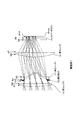
図6は、実施例1としての光学ブロック2の構成を示している。
なお図6において、図中の面Simgは、図1(及び図2)に示したイメージセンサ3の撮像面を表す。
また図6では赤外光の光線も併せて示している。
図中の短破線で示す光線は像高0mmに集光する光線を表し、丸破線で示す光線は像高1.5mmに集光する光線を表している。
また実線で示す光線は像高3.5mmに、長破線で示す光線は像高5.0mmにそれぞれ集光する光線を表す。
<2. Specific Example>
[2-1. Example 1]
FIG. 6 shows a configuration of the
In FIG. 6, a surface Simg in the drawing represents an imaging surface of the
FIG. 6 also shows infrared rays.
In the figure, a light beam indicated by a short broken line represents a light beam condensed at an image height of 0 mm, and a light beam indicated by a circular broken line represents a light beam condensed at an image height of 1.5 mm.
A light beam indicated by a solid line represents a light beam condensed at an image height of 3.5 mm, and a light beam indicated by a long broken line represents a light beam condensed at an image height of 5.0 mm.
本実施例において、第1レンズ10と第3レンズ12はSi製とされ、第2レンズ11は高分子量ポリエチレン製とされる。
ここで、本例では、イメージセンサ3の直前位置に平坦な部材によるカバーガラス14を設けることとしている。このカバーガラス14は、イメージセンサ3の撮像面保護のために設けられるものである。
当該カバーガラス14としても、Si製とする(赤外光を透過させるため)。
In the present embodiment, the
Here, in this example, a
The
本実施例の場合、第1レンズ10は、物体側に球面形状、像面側に平面形状をもつ平凸レンズとされ、正の屈折力を有する。
第2レンズ11は、両面とも非球面形状をもち、像面側に凸となるメニスカス形状レンズである。
また第3レンズ12は、物体面側に球面形状、像面側に平面形状を有する平凸レンズとされ、正の屈折力を有する。
In this embodiment, the
The
The
また本実施例において、開口絞り13は第1レンズ10と第2レンズ11との間に配置される。すなわち、このように第1レンズ10〜第3レンズ12の間に開口絞り13を設けることで、第1レンズ10又は第3レンズ12の有効径が大きくならないようにしている。
In this embodiment, the
さらにこの場合、シャッタ(図示は省略)は開口絞り13の位置に配される。このように開口絞り位置にシャッタが配されることで、赤外線検出素子に焦電素子を用いた構成において、光量ムラの発生の防止が図られる。
また、第1レンズ10と第2レンズ11との間に開口絞り13が設けられた上で、開口絞り位置にシャッタが配置された構成とされていることで、樹脂製の第2レンズ11に吸収された熱に起因するS/Nの悪化の防止が図られる。
Further, in this case, a shutter (not shown) is disposed at the position of the
In addition, since the
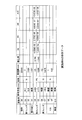
実施例1における各レンズの形状(及び開口絞り13)についての係数、及び面間隔を図7に示す。
ここで、非球面レンズに関して、レンズ面の凹凸は、半径rを用いて次のように表される。
ただし、Z(r)は光軸を中心としたときの半径rの点におけるレンズ面の高さを示す。面の高さは、物体側を負、像面側を正としている。Rは曲率半径、kは離心率、A4、A6、A8、A10、・・・は非球面係数である。
FIG. 7 shows the coefficients for the shape of each lens (and the aperture stop 13) and the surface interval in Example 1.
Here, regarding the aspherical lens, the unevenness of the lens surface is expressed as follows using the radius r.
Here, Z (r) indicates the height of the lens surface at the point of the radius r when the optical axis is the center. The height of the surface is negative on the object side and positive on the image surface side. R is a radius of curvature, k is an eccentricity, A4, A6, A8, A10,... Are aspherical coefficients.
図7において、面S0は物体面を表し、本例では最も物体側に配置される第1レンズ1
0から9000mm離れた位置に設定している。
面S1、面S2は、第1レンズ10の物体側の面、像面側の面をそれぞれ表す。面S3
は開口絞り13の面を表し、面S4、面S5はそれぞれ第2レンズ11の物体側の面、像
面側の面を表す。また、面S6、面S7は第3レンズ12の物体側の面、像面側の面であ
る。さらに面S8、面S9はカバーガラス(CG)14の物体側の面、像面側の面である
。これら面S8,S9は共に平坦面となる。
また、面S10=面Simgである。
In FIG. 7, a surface S0 represents an object surface, and in this example, the
It is set at a position away from 0 to 9000 mm.
Surface S1 and surface S2 represent the object-side surface and the image-side surface of the
Represents the surface of the
Further, surface S10 = surface Simg.
実施例1において、第1レンズ10及び第3レンズ12で用いるSiの屈折率は3.4212、第2レンズ11で用いるポリエチレンの屈折率は1.54である。
また、開口絞り13の直径は12.98mm、焦点距離は14.9mmとし、Fナンバー=1.09、水平画角30.1°を実現している。
In Example 1, the refractive index of Si used in the
The
図8は、実施例1の光学ブロック2についての各像高(0mm、1.5mm、3.5mm、5.0mm)における分解能特性(MTF)を示している。
具体的にこの図では、各像高における特性を横軸を空間周波数(lines/mm)、縦軸をOTF(Optical Transfer Function)として表している。
なおこの図においても像高0mmが短破線、像高1.5mmが丸破線、像高3.5mmが実線、像高5.0mmが長破線である。また、図中「T」の表記はタンジェンシャル値を意味し、「S」の表記はサジタル値を意味する。
FIG. 8 shows resolution characteristics (MTF) at each image height (0 mm, 1.5 mm, 3.5 mm, 5.0 mm) for the
Specifically, in this figure, the characteristics at each image height are represented by the horizontal axis representing the spatial frequency (lines / mm) and the vertical axis representing the OTF (Optical Transfer Function).
Also in this figure, the
ここで、像高5.0mmを10割とした場合、0割にあたる像高0mmと、3割にあたる像高1.5mmとで、20lines/mmにおけるMTF値(OTF値)が0.3以上となり、且つ、7割にあたる像高3.5mmで10lines/mmにおけるMTF値が0.3以上となることが望ましい。 Here, if the image height is 5.0%, the MTF value (OTF value) at 20 lines / mm is 0.3 or more at an image height of 0 mm corresponding to 0% and an image height of 1.5 mm corresponding to 30%. In addition, it is desirable that the MTF value at 10 lines / mm is 0.3 or more at an image height of 3.5 mm corresponding to 70%.
本実施例の赤外線光学系では、像高0mmにおける20lines/mmでのMTF値が0.457、像高1.5mmにおける20lines/mmでのMTFのタンジェンシャル値0.496、サジタル値0.544、像高3.5mmにおける10lines/mmにおけるMTFのタンジェンシャル値0.434、サジタル値0.619と、高い分解能が得られている。 In the infrared optical system of this embodiment, the MTF value at 20 lines / mm at an image height of 0 mm is 0.457, the tangential value of MTF at 20 lines / mm at an image height of 1.5 mm is 0.496, and the sagittal value is 0.544. A high resolution of MTF tangential value 0.434 and sagittal value 0.619 at 10 lines / mm at an image height of 3.5 mm is obtained.
このような実施例1としての光学系では、比較的安価な材料であるシリコンを用いて、加工コストの抑えられる平面または球面形状をもつ第1レンズ10及び第3レンズ12を作成して光学系のパワーを担当させ、加工が容易なポリエチレンを用いて、非球面形状の第2レンズ11を作成して収差を補正している。
ポリエチレンは、シリコンに比べ透過率が低い材質ではあるが、ポリエチレンレンズの使用を1枚に抑え、第2レンズ11の最大光線長を1.17mm(つまり2.0mm以下)に抑えることにより、透過率の低下を抑制している。さらに焦点距離を14.9mmと短くすることにより、色収差の影響を抑えつつ、波長8〜12μm帯において十分な分解能性能を得ることができている。
In the optical system as Example 1 as described above, the
Polyethylene is a material with a lower transmittance than silicon, but it can be transmitted by limiting the use of a polyethylene lens to one and the maximum light length of the
また、開口絞り位置にシャッタを置くことで、第2レンズ11からイメージセンサ3に入る放射熱量は変化せず、入射熱量の変化量を検知する焦電素子を使用した場合、第2レンズ11からの放射熱量が検知されないようにできる。ポリエチレンは通常赤外線の吸収がシリコン等に比べると多く、それはつまり放射熱量が多いことになるが、本実施例の構成を採ることにより、光学系のS/Nの悪化を効果的に抑制できる。
In addition, by placing a shutter at the aperture stop position, the amount of radiant heat that enters the
以上のように本実施例によれば、コストアップを抑えつつ、画角30°近い広画角を図りながら、十分な分解能性能を得ることができる。
As described above, according to the present embodiment, it is possible to obtain sufficient resolution performance while suppressing a cost increase and achieving a wide angle of view close to 30 °.
[2-2.実施例2]
図9は、実施例2としての光学ブロック2の構成を示している。
なお、図9においても各像高(0mm、1.5mm、3.5mm、5.0mm)に集光する赤外光の光線を併せて示している。この場合も像高0mm=短破線、像高1.5mm=丸破線、像高3.5mm=実線、像高5.0mm=長破線となる。
[2-2. Example 2]
FIG. 9 shows a configuration of the
Note that FIG. 9 also shows infrared rays condensed at respective image heights (0 mm, 1.5 mm, 3.5 mm, and 5.0 mm). Also in this case, the image height is 0 mm = short broken line, the image height is 1.5 mm = round broken line, the image height is 3.5 mm = solid line, and the image height is 5.0 mm = long broken line.
図9において、実施例2においても、物体側よりシリコン製の第1レンズ10、高分子量ポリエチレン製の第2レンズ11、シリコン製の第3レンズ12、及びシリコン製のカバーガラス14を配置している。
但し実施例2では、開口絞り13の位置を、第2レンズ11と第3レンズ12との間としている。
この場合も、開口絞り13の位置が第1レンズ10〜第3レンズ12の何れかの間とされていることで、第1レンズ10又は第3レンズ12の有効径が大きくならないようにしている。
In FIG. 9, also in Example 2, the
However, in Example 2, the position of the
Also in this case, the effective diameter of the
この場合、第1レンズ10は両面に球面をもち、物体側に凸となるメニスカス形状レンズとされる。
また第3レンズ12は両面に球面をもち、像面側に凸となるメニスカス形状レンズとされる。
なお、第1レンズ10及び第3レンズ12は共に正の屈折力を有する。
また第2レンズ11は、この場合も両面非球面形状であり、像面側に凸となるメニスカスレンズである。
In this case, the
The
Both the
Also in this case, the
ここで、実施例2では、樹脂レンズである第2レンズ11のフランジ(外周部)を物体側・像面側共に平面に加工するものとしている。その上で、図示するように3枚のレンズの外径は揃えるものとし、上記フランジの平面部を利用して、スペーサを介して3枚のレンズを所定間隔で同一鏡筒内に設置するものとしている。
このように各レンズの外径を揃え、スペーサを用いた収納とすることで、レンズ間の偏芯を抑えた組立てを容易に実現することができる。
なお、この点については、以降で説明する実施例3〜実施例6においても同様である。
Here, in Example 2, the flange (outer peripheral portion) of the
As described above, by aligning the outer diameters of the respective lenses and using the spacers for the storage, it is possible to easily realize an assembly in which the eccentricity between the lenses is suppressed.
This also applies to Examples 3 to 6 described below.
また、本実施例においても、シャッタ(図示は省略)は開口絞り13の位置に配される。このように開口絞り位置にシャッタが配されることで、赤外線検出素子に焦電素子を用いた構成において、光量ムラの発生の防止が図られる。
Also in this embodiment, the shutter (not shown) is arranged at the position of the
実施例2の場合の各レンズの形状(及び開口絞り13)についての係数及び面間隔を図10に示す。
なお、面番号の定義は、実施例1の場合との比較で以下のように変更となる。
すなわち本実施例の場合、面S3、面S4がそれぞれ第2レンズ11の物体側面、像面側面となり、面S5が開口絞り13の面となる。
FIG. 10 shows the coefficients and the surface intervals for the shape of each lens (and the aperture stop 13) in Example 2.
The definition of the surface number is changed as follows in comparison with the case of the first embodiment.
That is, in this embodiment, the surface S3 and the surface S4 are the object side surface and the image surface side surface of the
図10において、この場合も物体面である面S0から面S1までの距離は9000mmとしている。
なおこの場合としても、第1レンズ10及び第3レンズ12で用いるシリコンの屈折率、及び第2レンズ11で用いるポリエチレンの屈折率については実施例1の場合と同様となる。また焦点距離も実施例1の場合と同様である。
この場合、開口絞り13の直径は13.24mmであり、Fナンバーは1.11である。水平画角については実施例1の場合と同様の30.1°である。
In FIG. 10, the distance from the object surface S0 to the surface S1 is 9000 mm in this case as well.
Even in this case, the refractive index of silicon used in the
In this case, the diameter of the
図11は、実施例2の光学ブロック2についての各像高(0mm、1.5mm、3.5mm、5.0mm)における分解能特性(MTF)を示している。
なおこの図においても横軸=空間周波数(lines/mm)、縦軸=OTFである。
FIG. 11 shows resolution characteristics (MTF) at each image height (0 mm, 1.5 mm, 3.5 mm, 5.0 mm) for the
Also in this figure, the horizontal axis = spatial frequency (lines / mm) and the vertical axis = OTF.
実施例2の光学系では、像高0mmにおける20lines/mmでのMTF値が0.631、像高1.5mmにおける20lines/mmでのMTFのタンジェンシャル値0.609、サジタル値0.637、像高3.5mmにおける10lines/mmにおけるMTFのタンジェンシャル値0.667、サジタル値0.776と、高い分解能が得られている。 In the optical system of Example 2, the MTF value at 20 lines / mm at an image height of 0 mm is 0.631, the tangential value of MTF at 20 lines / mm at an image height of 1.5 mm is 0.609, the sagittal value is 0.637, A high resolution of 0.667 MTF tangential value and sagittal value 0.776 at 10 lines / mm at an image height of 3.5 mm is obtained.
上記による実施例2の光学系においても、比較的安価な材料であるシリコンを用いて、加工コストの抑えられる平面または球面形状をもつ第1レンズ10及び第3レンズ12を作成して光学系のパワーを担当させ、加工が容易なポリエチレンを用いて、非球面形状の第2レンズ11を作成して収差を補正している。
そしてこの場合も、ポリエチレンレンズの使用を1枚に抑え、第2レンズ11の最大光線長は1.96mmに抑えることにより、透過率の低下を抑制している。さらに焦点距離を14.9mmと短くすることにより、色収差の影響を抑えつつ、波長8〜12μm帯において十分な分解能性能を得ることができている。
Also in the optical system of Example 2 according to the above, the
Also in this case, the use of the polyethylene lens is suppressed to one, and the maximum light ray length of the
また実施例2では、第1レンズ10、第3レンズ12はメニスカスレンズであるが、平板状のシリコンから研磨して凹面側(つまりそれぞれ第2レンズ11と向き合う側)を作成することで、凹面側の外周に平面部分を確保することができる。第1レンズ10の凸面を物体側に、第3レンズ12の凸面を像面側に向けることにより、上記凹面側の平面部分が向き合う形となる。これにより、前述のスペーサを用いたレンズ間隔の調整を行う場合により好適となる。
In Example 2, the
以上のように実施例2の構成によっても、コストアップを抑えつつ、画角30°近い広画角を図りながら、十分な分解能性能を得ることができる。
As described above, even with the configuration of the second embodiment, it is possible to obtain sufficient resolution performance while suppressing a cost increase and achieving a wide angle of view close to 30 °.
[2-3.実施例3]
図12は、実施例3としての光学ブロック2の構成を示している。
なお、図12においても、各像高(0mm、1.5mm、3.5mm、5.0mm)に集光する赤外光の光線を併せて示している。この場合も像高0mm=短破線、像高1.5mm=丸破線、像高3.5mm=実線、像高5.0mm=長破線である。
[2-3. Example 3]
FIG. 12 shows a configuration of the
Note that FIG. 12 also shows infrared rays condensed at each image height (0 mm, 1.5 mm, 3.5 mm, and 5.0 mm). Also in this case, the image height is 0 mm = short broken line, the image height is 1.5 mm = round broken line, the image height is 3.5 mm = solid line, and the image height is 5.0 mm = long broken line.
先ず、この場合の各レンズ、開口絞り13、及びカバーガラス14の配置関係は実施例2の場合と同様となる。また、各レンズの構成材料としても先の実施例2の場合と同様である。
First, the positional relationship among the lenses,
この場合、第1レンズ10、第3レンズ12は共に正のパワーを有し、第1レンズ10は物体側に球面形状、像面側に平面をもつ平凸レンズとされ、第3レンズ12は物体側に平面、像面側に球面形状をもつ平凸レンズとされる。
また第2レンズ11は、先の実施例2の場合と同様に両面とも非球面形状をもち、像面側に凸となるメニスカスレンズとされ、そのフランジには物体側・像面側共に平面を有する。
In this case, both the
Similarly to the second embodiment, the
この場合も実施例2と同様に第1レンズ10〜第3レンズ12の間に開口絞り13が設けられることで、第1レンズ10又は第3レンズ12の有効径が大きくならないように図られている。
Also in this case, similarly to the second embodiment, the
またこの場合、シャッタ(図示は省略)は開口絞り13の位置に配される。このように開口絞り位置にシャッタが配されることで、赤外線検出素子に焦電素子を用いた構成において、光量ムラの発生の防止が図られる。
In this case, a shutter (not shown) is disposed at the position of the
実施例3の場合の各レンズの形状(及び開口絞り13)についての係数及び面間隔を図13に示す。
なお、面番号の定義は実施例2の場合と同様である。
またこの場合、面S0としての物体面は、第1レンズ10から9000mm離れた位置に設定している。
FIG. 13 shows the coefficients and the surface spacing for each lens shape (and aperture stop 13) in the case of Example 3.
The definition of the surface number is the same as that in the second embodiment.
In this case, the object surface as the surface S0 is set at a position away from the
ここで、この場合としても、第1レンズ10及び第3レンズ12で用いるシリコンの屈折率、第2レンズ11で用いるポリエチレンの屈折率、焦点距離については実施例1,2の場合と同様となる。
本実施例の場合、開口絞り13の直径は13.75mmであり、Fナンバー1.06、水平画角については実施例1,2と同様に30.1°を実現している。
Here, also in this case, the refractive index of silicon used in the
In the case of the present embodiment, the diameter of the
図14は、実施例3の光学ブロック2についての各像高(0mm、1.5mm、3.5mm、5.0mm)における分解能特性(MTF)を示している。
なおこの図においても横軸=空間周波数(lines/mm)、縦軸=OTFである。
FIG. 14 shows resolution characteristics (MTF) at image heights (0 mm, 1.5 mm, 3.5 mm, and 5.0 mm) for the
Also in this figure, the horizontal axis = spatial frequency (lines / mm) and the vertical axis = OTF.
実施例3の光学系では、像高0mmにおける20lines/mmでのMTF値が0.640、像高1.5mmにおける20lines/mmでのMTFのタンジェンシャル値0.661、サジタル値0.679、像高3.5mmにおける10lines/mmでのMTFのタンジェンシャル値0.676、サジタル値0.700と、高い分解能が得られている。 In the optical system of Example 3, the MTF value at 20 lines / mm at an image height of 0 mm is 0.640, the tangential value of MTF at 20 lines / mm at an image height of 1.5 mm is 0.661, the sagittal value is 0.679, A high resolution of MTF tangential value of 0.676 and sagittal value of 0.700 at 10 lines / mm at an image height of 3.5 mm is obtained.
上記による実施例3の光学系においても、比較的安価な材料であるシリコンを用いて、加工コストの抑えられる平面または球面形状をもつ第1レンズ10及び第3レンズ12を作成して光学系のパワーを担当させ、加工が容易なポリエチレンを用いて、非球面形状の第2レンズ11を作成して収差を補正している。
この場合もポリエチレンレンズの使用を1枚に抑え、第2レンズ11の最大光線長については1.68mmに抑えることにより、透過率の低下を抑制している。
さらに焦点距離を14.9mmと短くすることにより、色収差の影響を抑えつつ、波長8〜12μm帯において十分な分解能性能を得ることができている。
Also in the optical system of Example 3 according to the above, the
Also in this case, the use of the polyethylene lens is suppressed to one, and the maximum light ray length of the
Further, by shortening the focal length to 14.9 mm, it is possible to obtain sufficient resolution performance in the wavelength band of 8 to 12 μm while suppressing the influence of chromatic aberration.
以上のように実施例3によっても、コストアップを抑えつつ、画角30°近い広画角を図りながら、十分な分解能性能を得ることができる。
As described above, according to the third embodiment, it is possible to obtain sufficient resolution performance while suppressing a cost increase and achieving a wide angle of view close to 30 °.
[2-4.実施例4]
図15は、実施例4としての光学ブロック2の構成を示している。
なお、図15においても、各像高(0mm、1.5mm、3.5mm、5.0mm)に集光する赤外光の光線を併せて示している。この場合も像高0mm=短破線、像高1.5mm=丸破線、像高3.5mm=実線、像高5.0mm=長破線である。
[2-4. Example 4]
FIG. 15 shows a configuration of the
FIG. 15 also shows infrared rays condensed at each image height (0 mm, 1.5 mm, 3.5 mm, 5.0 mm). Also in this case, the image height is 0 mm = short broken line, the image height is 1.5 mm = round broken line, the image height is 3.5 mm = solid line, and the image height is 5.0 mm = long broken line.
先ず、この場合の各レンズ、開口絞り13、及びカバーガラス14の配置関係は実施例1の場合と同様となる。また、各レンズの構成材料としても先の実施例1の場合と同様である。
First, the positional relationship among the lenses,
この場合、第1レンズ10、第3レンズ12は共に正のパワーを有し、第1レンズ10は両面に球面を有しかつ物体側に凸となるメニスカス形状レンズ、第3レンズ12は同様に両面に球面を有するが像面側に凸となるメニスカス形状レンズとされる。
また第2レンズ11は、先の実施例2の場合と同様に両面とも非球面形状を有するが、この場合は物体側に凸となるメニスカスレンズとされる。なおこの場合も、第2レンズ11のフランジは、実施例2の場合と同様に物体側・像面側共に平面を有するように加工されている。
In this case, both the
The
本実施例においても、実施例1の場合と同様、第1レンズ10〜第3レンズ12の間に開口絞り13が設けられることで、第1レンズ10又は第3レンズ12の有効径が大きくならないように図られている。
Also in the present embodiment, as in the case of the first embodiment, the effective diameter of the
またこの場合も、シャッタ(図示は省略)は開口絞り13の位置に配される。このように開口絞り位置にシャッタが配されることで、赤外線検出素子に焦電素子を用いた構成において、光量ムラの発生の防止が図られる。
また、第1レンズ10と第2レンズ11との間に開口絞り13が設けられた上で、開口絞り位置にシャッタが配置された構成とされていることで、樹脂製の第2レンズ11に吸収された熱に起因するS/Nの悪化の防止が図られる。
Also in this case, the shutter (not shown) is arranged at the position of the
In addition, since the
実施例4の場合の各レンズの形状(及び開口絞り13)についての係数及び面間隔を図16に示す。
なお、面番号の定義は実施例1の場合と同様である。
またこの場合、面S0としての物体面は、実施例1の場合と同様に第1レンズ10から9000mm離れた位置に設定している。
FIG. 16 shows the coefficients and the surface intervals for the shape of each lens (and the aperture stop 13) in Example 4.
The definition of the surface number is the same as in the first embodiment.
In this case, the object surface as the surface S0 is set at a
ここで、この場合としても、第1レンズ10及び第3レンズ12で用いるシリコンの屈折率、第2レンズ11で用いるポリエチレンの屈折率、焦点距離については実施例1の場合と同様となる。
本実施例の場合、開口絞り13の直径は12.24mmであり、Fナンバーは1.06である。水平画角については30.1°と、実施例1,2と同様の数値を実現している。
Here, also in this case, the refractive index of silicon used for the
In the case of the present embodiment, the diameter of the
図17は、実施例4の光学ブロック2についての各像高(0mm、1.5mm、3.5mm、5.0mm)における分解能特性(MTF)を示している。
なおこの図においても横軸=空間周波数(lines/mm)、縦軸=OTFである。
FIG. 17 shows resolution characteristics (MTF) at image heights (0 mm, 1.5 mm, 3.5 mm, and 5.0 mm) for the
Also in this figure, the horizontal axis = spatial frequency (lines / mm) and the vertical axis = OTF.
実施例4の光学系では、像高0mmにおける20lines/mmでのMTF値が0.621、像高1.5mmにおける20lines/mmでのMTFのタンジェンシャル値0.566、サジタル値0.534、像高3.5mmにおける10lines/mmでのMTFのタンジェンシャル値0.677、サジタル値0.654と、高い分解能が得られている。 In the optical system of Example 4, the MTF value at 20 lines / mm at an image height of 0 mm is 0.621, the tangential value of MTF at 20 lines / mm at an image height of 1.5 mm is 0.566, the sagittal value is 0.534, A high resolution of MTF tangential value 0.677 and sagittal value 0.654 at 10 lines / mm at an image height of 3.5 mm is obtained.
上記による実施例4の光学系においても、比較的安価な材料であるシリコンを用いて、加工コストの抑えられる平面または球面形状をもつ第1レンズ10及び第3レンズ12を作成して光学系のパワーを担当させ、加工が容易なポリエチレンを用いて、非球面形状の第2レンズ11を作成して収差を補正している。
この場合もポリエチレンレンズの使用を1枚に抑え、第2レンズ11の最大光線長については1.70mmに抑えることにより、透過率の低下を抑制している。
さらに焦点距離を14.9mmと短くすることにより、色収差の影響を抑えつつ、波長8〜12μm帯において十分な分解能性能を得ることができている。
Also in the optical system of Example 4 according to the above, the
Also in this case, the use of the polyethylene lens is suppressed to one, and the maximum ray length of the
Further, by shortening the focal length to 14.9 mm, it is possible to obtain sufficient resolution performance in the wavelength band of 8 to 12 μm while suppressing the influence of chromatic aberration.
また実施例4では、第1レンズ10、第3レンズ12はメニスカスレンズであるが、先の実施例2と同様、平板状のシリコンから研磨して凹面側(それぞれ第2レンズ11と向き合う側)を作成することで、凹面側の外周に平面部分を確保することができる。第1レンズ10の凸面を物体側に、第3レンズ12の凸面を像面側に向けることにより、上記凹面側の平面部分が向き合う形となる。すなわち、前述のスペーサを用いたレンズ間隔の調整を行う場合により好適となる。
In the fourth embodiment, the
以上のように実施例4によっても、コストアップを抑えつつ、画角30°近い広画角を図りながら、十分な分解能性能を得ることができる。
As described above, according to the fourth embodiment, it is possible to obtain sufficient resolution performance while suppressing a cost increase and achieving a wide angle of view close to 30 °.
[2-5.実施例5]
図18は、実施例5としての光学ブロック2の構成を示している。
なお、図18においても各像高(0mm、1.5mm、3.5mm、5.0mm)に集光する赤外光の光線を併せて示している。この場合も像高0mm=短破線、像高1.5mm=丸破線、像高3.5mm=実線、像高5.0mm=長破線である。
[2-5. Example 5]
FIG. 18 shows a configuration of the
Note that FIG. 18 also shows the rays of infrared light condensed at each image height (0 mm, 1.5 mm, 3.5 mm, and 5.0 mm). Also in this case, the image height is 0 mm = short broken line, the image height is 1.5 mm = round broken line, the image height is 3.5 mm = solid line, and the image height is 5.0 mm = long broken line.
この場合の各レンズ、開口絞り13、及びカバーガラス14の配置関係は実施例1の場合と同様となる。
この場合、第1レンズ10、第3レンズ12としてはゲルマニウム(Ge)製のレンズを用いる。
第2レンズ11については本実施例の場合も高分子量ポリエチレンレンズを用いる。またカバーガラス14も先の各実施例と同様のシリコン製のものを用いる。
In this case, the positional relationship among the lenses, the
In this case, germanium (Ge) lenses are used as the
As for the
この場合、第1レンズ10、第3レンズ12は共に正のパワーを有し、第1レンズ10は物体側に凸となるメニスカス形状レンズ、第3レンズ12は物体側に平面、像面側に球面形状をもつ平凸レンズとされる。
また第2レンズ11は、両面とも非球面形状をもち、物体側に凸となるメニスカスレンズとされる。そしてそのフランジは、先の実施例2の場合と同様に物体側・像面側共に平面を有するように加工されている。
In this case, both the
Further, the
先の各実施例の場合と同様、第1レンズ10〜第3レンズ12の間に開口絞り13が設けられることで、第1レンズ10又は第3レンズ12の有効径が大きくならないように図られている。
As in the previous embodiments, the effective diameter of the
またこの場合も、シャッタ(図示は省略)は開口絞り13の位置に配される。このように開口絞り位置にシャッタが配されることで、赤外線検出素子に焦電素子を用いた構成において、光量ムラの発生の防止が図られる。
また、第1レンズ10と第2レンズ11との間に開口絞り13が設けられた上で、開口絞り位置にシャッタが配置された構成とされていることで、樹脂製の第2レンズ11に吸収された熱に起因するS/Nの悪化の防止が図られる。
Also in this case, the shutter (not shown) is arranged at the position of the
In addition, since the
実施例5の場合の各レンズの形状(及び開口絞り13)についての係数及び面間隔を図19に示す。
なお、面番号の定義は実施例1の場合と同様である。
またこの場合、面S0としての物体面は、第1レンズ10から80000mm離れた位置に設定している。
FIG. 19 shows the coefficients and the surface intervals for the shape of each lens (and the aperture stop 13) in Example 5.
The definition of the surface number is the same as in the first embodiment.
In this case, the object surface as the surface S0 is set at a
ここで、実施例5において第1レンズ10及び第3レンズ12で用いるゲルマニウムの屈折率は4.0である。
なお、第2レンズ11で用いるポリエチレンの屈折率、及び焦点距離については先の各実施例の場合と同様となる。
また本実施例の場合、開口絞り13の直径は11.58mmであり、Fナンバーは1.06である。水平画角については先の各実施例と同様に30.1°を実現している。
Here, in Example 5, the refractive index of germanium used for the
The refractive index and focal length of polyethylene used in the
In the present embodiment, the diameter of the
図20は、実施例5の光学ブロック2についての各像高(0mm、1.5mm、3.5mm、5.0mm)における分解能特性(MTF)を示している。
なおこの図においても横軸=空間周波数(lines/mm)、縦軸=OTFである。
FIG. 20 shows the resolution characteristics (MTF) at each image height (0 mm, 1.5 mm, 3.5 mm, 5.0 mm) for the
Also in this figure, the horizontal axis = spatial frequency (lines / mm) and the vertical axis = OTF.
実施例5の光学系では、像高0mmにおける20lines/mmでのMTF値が0.656、像高1.5mmにおける20lines/mmでのMTFのタンジェンシャル値0.713、サジタル値0.704、像高3.5mmにおける10lines/mmでのMTFのタンジェンシャル値0.592、サジタル値0.701と、高い分解能が得られている。 In the optical system of Example 5, the MTF value at 20 lines / mm at an image height of 0 mm is 0.656, the tangential value of MTF at 20 lines / mm at an image height of 1.5 mm is 0.713, the sagittal value is 0.704, A high resolution of MTF tangential value 0.592 and sagittal value 0.701 at 10 lines / mm at an image height of 3.5 mm is obtained.
上記による実施例5の光学系においては、加工コストの抑えられる平面または球面形状をもつ第1レンズ10及び第3レンズ12を作成して光学系のパワーを担当させ、加工が容易なポリエチレンを用いて、非球面形状の第2レンズ11を作成して収差を補正している。
この場合もポリエチレンレンズの使用を1枚に抑え、第2レンズ11の最大光線長については1.48mmに抑えることにより、透過率の低下を抑制している。
さらに焦点距離を14.9mmと短くすることにより、色収差の影響を抑えつつ、波長8〜12μm帯において十分な分解能性能を得ることができている。
In the optical system of Example 5 according to the above, the
Also in this case, the use of a polyethylene lens is suppressed to one and the maximum light ray length of the
Further, by shortening the focal length to 14.9 mm, it is possible to obtain sufficient resolution performance in the wavelength band of 8 to 12 μm while suppressing the influence of chromatic aberration.
また実施例5では、第1レンズ10がメニスカスレンズであるが、先の実施例2と同様、平板状の母材(この場合はゲルマニウム)から研磨して凹面側(第2レンズ11と向き合う側)を作成することで、凹面側の外周に平面部分を確保することができる。これにより、前述のスペーサを用いたレンズ間隔の調整を行う場合により好適となる。
In the fifth embodiment, the
以上のように実施例5によっても、コストアップを抑えつつ、画角30°近い広画角を図りながら、十分な分解能性能を得ることができる。
As described above, according to the fifth embodiment, it is possible to obtain sufficient resolution performance while suppressing a cost increase and achieving a wide angle of view close to 30 °.
[2-6.実施例6]
図21は、実施例6としての光学ブロック2の構成を示している。
なお、図21においても、各像高(0mm、1.5mm、3.5mm、5.0mm)に集光する赤外光の光線を併せて示している。この場合も像高0mm=短破線、像高1.5mm=丸破線、像高3.5mm=実線、像高5.0mm=長破線である。
[2-6. Example 6]
FIG. 21 shows a configuration of the
Note that FIG. 21 also shows infrared rays condensed at each image height (0 mm, 1.5 mm, 3.5 mm, and 5.0 mm). Also in this case, the image height is 0 mm = short broken line, the image height is 1.5 mm = round broken line, the image height is 3.5 mm = solid line, and the image height is 5.0 mm = long broken line.
先ず、この場合の各レンズ、開口絞り13、及びカバーガラス14の配置関係は実施例1の場合と同様となる。また、各レンズの構成材料としても先の実施例1の場合と同様である。
First, the positional relationship among the lenses,
この場合、第1レンズ10、第3レンズ12は共に正のパワーを有し、第1レンズ10は両面に非球面をもつ物体側に凸となるメニスカス形状レンズとされ、第3レンズ12は物体側に平面、像面側に球面形状をもつ平凸レンズとされる。
また第2レンズ11は、両面とも非球面形状をもち物体側に凸となるメニスカス形状レンズとされ、そのフランジには、先の実施例2と同様に物体側・像面側共に平面が形成される。
In this case, both the
The
先の各実施例の場合と同様、第1レンズ10〜第3レンズ12の間に開口絞り13が設けられることで、第1レンズ10又は第3レンズ12の有効径が大きくならないように図られている。
As in the previous embodiments, the effective diameter of the
またこの場合も、シャッタ(図示は省略)は開口絞り13の位置に配される。このように開口絞り位置にシャッタが配されることで、赤外線検出素子に焦電素子を用いた構成において、光量ムラの発生の防止が図られる。
また、第1レンズ10と第2レンズ11との間に開口絞り13が設けられた上で、開口絞り位置にシャッタが配置された構成とされていることで、樹脂製の第2レンズ11に吸収された熱に起因するS/Nの悪化の防止が図られる。
Also in this case, the shutter (not shown) is arranged at the position of the
In addition, since the
実施例6の場合の各レンズの形状(及び開口絞り13)についての係数及び面間隔を図22に示す。
なお、面番号の定義は実施例1の場合と同様である。
またこの場合、面S0としての物体面は、第1レンズ10から80000mm離れた位置に設定している。
FIG. 22 shows the coefficients and the surface intervals for the shape of each lens (and the aperture stop 13) in Example 6.
The definition of the surface number is the same as in the first embodiment.
In this case, the object surface as the surface S0 is set at a
ここで、この場合としても、第1レンズ10及び第3レンズ12で用いるシリコンの屈折率、第2レンズ11で用いるポリエチレンの屈折率、焦点距離については実施例1の場合と同様となる。
本実施例の場合、開口絞り13の直径は11.98mmであり、Fナンバー1.06、水平画角については各実施例と同様の30.1°を実現している。
Here, also in this case, the refractive index of silicon used for the
In the case of the present embodiment, the diameter of the
図23は、実施例6の光学ブロック2についての各像高(0mm、1.5mm、3.5mm、5.0mm)における分解能特性(MTF)を示している。
なおこの図においても横軸=空間周波数(lines/mm)、縦軸=OTFである。
FIG. 23 shows the resolution characteristics (MTF) at each image height (0 mm, 1.5 mm, 3.5 mm, 5.0 mm) for the
Also in this figure, the horizontal axis = spatial frequency (lines / mm) and the vertical axis = OTF.
実施例6の光学系では、像高0mmにおける20lines/mmでのMTF値が0.684、像高1.5mmにおける20lines/mmでのMTFのタンジェンシャル値0.710、サジタル値0.713、像高3.5mmにおける10lines/mmでのMTFのタンジェンシャル値0.631、サジタル値0.615と、高い分解能が得られている。 In the optical system of Example 6, the MTF value at 20 lines / mm at an image height of 0 mm is 0.684, the tangential value of MTF at 20 lines / mm at an image height of 1.5 mm is 0.710, the sagittal value is 0.713, A high resolution of MTF tangential value 0.631 and sagittal value 0.615 at 10 lines / mm at an image height of 3.5 mm is obtained.
上記による実施例6の光学系においても、先の実施例1等と同様に比較的安価な材料であるシリコンを用いて、加工コストの抑えられる平面または球面形状をもつ第1レンズ10及び第3レンズ12を作成して光学系のパワーを担当させ、加工が容易なポリエチレンを用いて、非球面形状の第2レンズ11を作成して収差を補正している。
この場合もポリエチレンレンズの使用を1枚に抑え、第2レンズ11の最大光線長については1.55mmに抑えることにより、透過率の低下を抑制している。
さらに焦点距離を14.9mmと短くすることにより、色収差の影響を抑えつつ、波長8〜12μm帯において十分な分解能性能を得ることができている。
Also in the optical system of Example 6 according to the above, the
Also in this case, the use of the polyethylene lens is suppressed to one, and the maximum light ray length of the
Further, by shortening the focal length to 14.9 mm, it is possible to obtain sufficient resolution performance in the wavelength band of 8 to 12 μm while suppressing the influence of chromatic aberration.
また実施例6においても、第1レンズ10がメニスカスレンズとされるが、先の実施例5と同様、平板状のシリコンから研磨して凹面側を作成することで、凹面側の外周に平面部分を確保することができる。これにより、前述のスペーサを用いたレンズ間隔の調整を行う場合により好適となる。
Also in Example 6, the
以上のように実施例6によっても、コストアップを抑えつつ、画角30°近い広画角を図りながら、十分な分解能性能を得ることができる。
As described above, according to the sixth embodiment, it is possible to obtain sufficient resolution performance while suppressing a cost increase and achieving a wide angle of view close to 30 °.
<3.変形例>
以上、本技術の赤外線光学系及び赤外線撮像装置の実施の形態について説明したが、本技術としてはこれまでで説明した具体例に限定されるべきものではない。
例えば、各実施例においては、第2レンズ11で用いる樹脂材料としてポリエチレンを例示したが、これに限るものではなく、遠赤外領域での透過率を改善した樹脂材料であれば他の樹脂材料を適用可能である。
具体的に、第2レンズ11として用いる樹脂材料としては、例えば厚さ2.0mmでの透過率(波長8μm〜12μm)が20%以上となるような比較的高透過率の特性によるものを用いればよい。
<3. Modification>
The embodiments of the infrared optical system and the infrared imaging device of the present technology have been described above, but the present technology should not be limited to the specific examples described above.
For example, in each embodiment, polyethylene is exemplified as the resin material used in the
Specifically, as the resin material used for the
また、第1レンズ10及び第3レンズ12を構成する無機材料として、それぞれに同一の材料を用いる場合を例示したが、それぞれに異なる材料を用いることもできる。
Moreover, although the case where the same material was used for each was illustrated as an inorganic material which comprises the
また、これまでの説明では赤外線検出素子として焦電素子を備えたイメージセンサ3を用いる場合に対応して、光学系にシャッタを配置する例を挙げたが、例えばボロメータ型等の温度自体に応じた値を出力する素子を用いる場合には、シャッタが省略可能であることは言うまでも無い。
In the above description, an example in which a shutter is disposed in the optical system corresponding to the case where the
また、本技術については以下に示す構成とすることもできる。
(1)
物体側から像面側にかけて配置された第1レンズ、第2レンズ、第3レンズの3枚のレンズで構成され、
前記第1レンズ及び前記第3レンズが、無機材料で構成された正の屈折力を有する球面レンズとされ、
前記第2レンズが、樹脂材料で構成されたメニスカス形状の両面非球面レンズとされると共に、
前記第1レンズから前記第3レンズの間に開口絞りが設けられ、
前記第2レンズは、その内部を透過し結像に寄与する光線の最大光線長が2.0mm以下となるように構成されている
赤外線光学系。
(2)
前記第2レンズはポリエチレンで構成されている
前記(1)に記載の赤外線光学系。
(3)
前記開口絞り位置にシャッタが設けられている
前記(1)又は(2)に記載の赤外線光学系。
(4)
前記開口絞りが前記第1レンズと前記第2レンズとの間に設けられ、且つ前記開口絞り位置にシャッタが設けられている
前記(1)〜(3)の何れかに記載の赤外線光学系。
(5)
前記第1レンズ、前記第3レンズは、平凸レンズ又はメニスカス形状レンズとされる
前記(1)〜(4)の何れかに記載の赤外線光学系。
(6)
物体側から像面側にかけて配置された第1レンズ、第2レンズ、第3レンズの3枚のレンズで構成され、
前記第1レンズ及び前記第3レンズが、無機材料で構成された正の屈折力を有する球面レンズとされ、
前記第2レンズが、樹脂材料で構成されたメニスカス形状の両面非球面レンズとされると共に、
前記第1レンズから前記第3レンズの間に開口絞りが設けられ、
前記第1レンズと前記第3レンズが共に平凸レンズとされ、
前記第1レンズの凸面が物体側を向き、前記第3レンズの凸面が像面側を向いている
赤外線光学系。
(7)
前記第1レンズと前記第3レンズがシリコンで構成されている
前記(1)〜(6)の何れかに記載の赤外線光学系。
(8)
前記第2レンズの外周部を物体側・像面側共に平面に加工し、
前記第1レンズの外周部の第2レンズ側を平面に加工し、
前記第3レンズの外周部の第2レンズ側を平面に加工した
前記(1)〜(7)の何れかに記載の赤外線光学系。
(9)
前記(1)〜(8)の何れかに記載の赤外線光学系を備えると共に、
前記赤外線光学系により集光された赤外光を検出する赤外線検出部と、
前記赤外線検出部により得られた赤外線検出信号に基づき赤外線撮像画像信号を得る画像信号取得部と
を備える赤外線撮像装置。
Further, the present technology may be configured as follows.
(1)
It is composed of three lenses, a first lens, a second lens, and a third lens, arranged from the object side to the image plane side.
The first lens and the third lens are spherical lenses having a positive refractive power made of an inorganic material,
The second lens is a meniscus double-sided aspheric lens made of a resin material,
An aperture stop is provided between the first lens and the third lens ;
The second lens is an infrared optical system configured so that a maximum light ray length of a light ray transmitted through the second lens and contributing to image formation is 2.0 mm or less .
(2)
The infrared optical system according to (1), wherein the second lens is made of polyethylene.
(3)
The infrared optical system according to (1) or (2), wherein a shutter is provided at the aperture stop position.
(4)
The infrared optical system according to any one of (1) to (3) , wherein the aperture stop is provided between the first lens and the second lens, and a shutter is provided at the aperture stop position.
(5)
The infrared optical system according to any one of (1) to (4) , wherein the first lens and the third lens are planoconvex lenses or meniscus lenses.
(6)
It is composed of three lenses, a first lens, a second lens, and a third lens, arranged from the object side to the image plane side.
The first lens and the third lens are spherical lenses having a positive refractive power made of an inorganic material,
The second lens is a meniscus double-sided aspheric lens made of a resin material,
An aperture stop is provided between the first lens and the third lens;
The first lens and the third lens are both plano-convex lenses;
The convex surface of the first lens faces the object side, and the convex surface of the third lens faces the image surface side.
Infrared optical system.
(7)
The infrared optical system according to any one of (1) to (6) , wherein the first lens and the third lens are made of silicon.
(8)
Processing the outer periphery of the second lens into a flat surface on both the object side and the image surface side;
Processing the second lens side of the outer periphery of the first lens into a plane;
The second lens side of the outer periphery of the third lens was processed into a flat surface.
The infrared optical system according to any one of (1) to (7).
(9)
While including the infrared optical system according to any one of (1) to (8),
An infrared detector for detecting infrared light collected by the infrared optical system;
An infrared imaging device comprising: an image signal acquisition unit that obtains an infrared imaging image signal based on an infrared detection signal obtained by the infrared detection unit.
1 赤外線撮像装置、2 光学ブロック、3 イメージセンサ、4 画像信号取得部、5 画像信号処理部、10 第1レンズ、11 第2レンズ、12 第3レンズ、13 開口絞り、14 カバーガラス
DESCRIPTION OF
Claims (9)
前記第1レンズ及び前記第3レンズが、無機材料で構成された正の屈折力を有する球面レンズとされ、
前記第2レンズが、樹脂材料で構成されたメニスカス形状の両面非球面レンズとされると共に、
前記第1レンズから前記第3レンズの間に開口絞りが設けられ、
前記第2レンズは、その内部を透過し結像に寄与する光線の最大光線長が2.0mm以下となるように構成されている
赤外線光学系。 It is composed of three lenses, a first lens, a second lens, and a third lens, arranged from the object side to the image plane side.
The first lens and the third lens are spherical lenses having a positive refractive power made of an inorganic material,
The second lens is a meniscus double-sided aspheric lens made of a resin material,
An aperture stop is provided between the first lens and the third lens ;
The second lens is an infrared optical system configured so that a maximum light ray length of a light ray transmitted through the second lens and contributing to image formation is 2.0 mm or less .
請求項1に記載の赤外線光学系。 The infrared optical system according to claim 1, wherein the second lens is made of polyethylene.
請求項1又請求項2に記載の赤外線光学系。 The infrared optical system according to claim 1, wherein a shutter is provided at the aperture stop position.
請求項1乃至請求項3の何れかに記載の赤外線光学系。 The infrared optical system according to any one of claims 1 to 3, wherein the aperture stop is provided between the first lens and the second lens, and a shutter is provided at the aperture stop position.
請求項1乃至請求項4の何れかに記載の赤外線光学系。 The infrared optical system according to any one of claims 1 to 4, wherein the first lens and the third lens are planoconvex lenses or meniscus lenses.
前記第1レンズ及び前記第3レンズが、無機材料で構成された正の屈折力を有する球面レンズとされ、The first lens and the third lens are spherical lenses having a positive refractive power made of an inorganic material,
前記第2レンズが、樹脂材料で構成されたメニスカス形状の両面非球面レンズとされると共に、The second lens is a meniscus double-sided aspheric lens made of a resin material,
前記第1レンズから前記第3レンズの間に開口絞りが設けられ、An aperture stop is provided between the first lens and the third lens;
前記第1レンズと前記第3レンズが共に平凸レンズとされ、The first lens and the third lens are both plano-convex lenses;
前記第1レンズの凸面が物体側を向き、前記第3レンズの凸面が像面側を向いているThe convex surface of the first lens faces the object side, and the convex surface of the third lens faces the image surface side.
赤外線光学系。Infrared optical system.
請求項1乃至請求項6の何れかに記載の赤外線光学系。 The infrared optical system according to any one of claims 1 to 6, wherein the first lens and the third lens are made of silicon.
前記第1レンズの外周部の第2レンズ側を平面に加工し、Processing the second lens side of the outer periphery of the first lens into a plane;
前記第3レンズの外周部の第2レンズ側を平面に加工したThe second lens side of the outer periphery of the third lens was processed into a flat surface.
請求項1乃至請求項7の何れかに記載の赤外線光学系。The infrared optical system according to any one of claims 1 to 7.
前記赤外線光学系により集光された赤外光を検出する赤外線検出部と、
前記赤外線検出部により得られた赤外線検出信号に基づき赤外線撮像画像信号を得る画像信号取得部と
を備える赤外線撮像装置。 A positive refraction in which the first lens, the second lens, and the third lens are arranged from the object side to the image plane side, and the first lens and the third lens are made of an inorganic material. A spherical lens having a force, the second lens is a meniscus double-sided aspherical lens made of a resin material, and an aperture stop is provided between the first lens and the third lens , The second lens has an infrared optical system configured so that the maximum light ray length of light rays that pass through the inside and contribute to image formation is 2.0 mm or less ;
An infrared detector for detecting infrared light collected by the infrared optical system;
An infrared imaging device comprising: an image signal acquisition unit that obtains an infrared imaging image signal based on an infrared detection signal obtained by the infrared detection unit.
Priority Applications (3)
| Application Number | Priority Date | Filing Date | Title |
|---|---|---|---|
| JP2011220408A JP5803532B2 (en) | 2011-10-04 | 2011-10-04 | Infrared optical system, infrared imaging device |
| US13/618,084 US9151934B2 (en) | 2011-10-04 | 2012-09-14 | Infrared optical system and infrared imaging apparatus |
| CN201210362420.5A CN103033909B (en) | 2011-10-04 | 2012-09-25 | Infrared optical system and infrared imaging device |
Applications Claiming Priority (1)
| Application Number | Priority Date | Filing Date | Title |
|---|---|---|---|
| JP2011220408A JP5803532B2 (en) | 2011-10-04 | 2011-10-04 | Infrared optical system, infrared imaging device |
Publications (3)
| Publication Number | Publication Date |
|---|---|
| JP2013080130A JP2013080130A (en) | 2013-05-02 |
| JP2013080130A5 JP2013080130A5 (en) | 2014-11-13 |
| JP5803532B2 true JP5803532B2 (en) | 2015-11-04 |
Family
ID=47992229
Family Applications (1)
| Application Number | Title | Priority Date | Filing Date |
|---|---|---|---|
| JP2011220408A Expired - Fee Related JP5803532B2 (en) | 2011-10-04 | 2011-10-04 | Infrared optical system, infrared imaging device |
Country Status (3)
| Country | Link |
|---|---|
| US (1) | US9151934B2 (en) |
| JP (1) | JP5803532B2 (en) |
| CN (1) | CN103033909B (en) |
Families Citing this family (18)
| Publication number | Priority date | Publication date | Assignee | Title |
|---|---|---|---|---|
| JP5617642B2 (en) * | 2011-01-06 | 2014-11-05 | ソニー株式会社 | Infrared optical system, infrared imaging device |
| US20130208353A1 (en) * | 2012-01-23 | 2013-08-15 | Jeremy Huddleston | Lwir imaging lens, image capturing system having the same, and associated methods |
| CN104603664B (en) * | 2012-09-05 | 2017-04-05 | 纳卢克斯株式会社 | Infrared ray image pickup optical system |
| JPWO2015029645A1 (en) * | 2013-08-28 | 2017-03-02 | コニカミノルタ株式会社 | Far-infrared lens, photographing lens system and camera system |
| WO2016051848A1 (en) | 2014-09-30 | 2016-04-07 | 富士フイルム株式会社 | Infrared imaging device, diaphragm control method, and diaphragm control program |
| CN106716991B (en) | 2014-09-30 | 2019-07-23 | 富士胶片株式会社 | Infrared pick-up device, image processing method and recording medium |
| WO2016072294A1 (en) * | 2014-11-05 | 2016-05-12 | コニカミノルタ株式会社 | Far infrared optical system, image-capturing optical device, and digital equipment |
| KR20160080509A (en) * | 2014-12-29 | 2016-07-08 | 삼성전기주식회사 | Illuminance sensor module |
| JP6397584B2 (en) * | 2015-12-03 | 2018-09-26 | 京セラオプテック株式会社 | Infrared imaging lens system |
| US10422976B2 (en) | 2016-02-26 | 2019-09-24 | Samsung Electronics Co., Ltd. | Aberration corrected optical system for near-eye displays |
| TWI676832B (en) * | 2017-04-21 | 2019-11-11 | 先進光電科技股份有限公司 | Optical image capturing system |
| CN109782422B (en) * | 2017-11-14 | 2021-02-26 | 新巨科技股份有限公司 | Three-piece infrared single-wavelength projection lens set |
| CN109782421B (en) * | 2017-11-14 | 2021-01-08 | 新巨科技股份有限公司 | Three-piece infrared single-wavelength projection lens set |
| US11454783B2 (en) | 2018-04-25 | 2022-09-27 | Samsung Electronics Co., Ltd. | Tiled triplet lenses providing a wide field of view |
| CN108919469A (en) * | 2018-08-03 | 2018-11-30 | 宁波舜宇红外技术有限公司 | Infrared measurement of temperature camera lens |
| US12001079B2 (en) | 2020-03-05 | 2024-06-04 | Sintai Optical (Shenzhen) Co., Ltd. | Optical camera lens |
| TWI740493B (en) * | 2020-05-11 | 2021-09-21 | 大陸商信泰光學(深圳)有限公司 | Optical camera lens |
| CN113371184A (en) * | 2021-06-11 | 2021-09-10 | 徐州楚创智能设备有限公司 | Intelligent observation aircraft for forest fire |
Family Cites Families (18)
| Publication number | Priority date | Publication date | Assignee | Title |
|---|---|---|---|---|
| US3160700A (en) * | 1961-08-18 | 1964-12-08 | John R Snyder | Infrared optical system |
| US5393482A (en) * | 1993-10-20 | 1995-02-28 | United Technologies Corporation | Method for performing multiple beam laser sintering employing focussed and defocussed laser beams |
| JPH10301024A (en) * | 1997-04-24 | 1998-11-13 | Mitsubishi Electric Corp | Infrared optical system |
| WO2000048033A1 (en) * | 1999-02-10 | 2000-08-17 | Matsushita Electric Industrial Co., Ltd. | Reflection optical device, reflection solid-state optical device, imaging device comprising this, multiwavelength imaging device, video camera, and monitoring device mounted on vehicle |
| JP2001290073A (en) * | 2000-04-04 | 2001-10-19 | Mitsubishi Electric Corp | Lens for infrared camera and infrared camera using the same |
| TW452658B (en) * | 2000-10-24 | 2001-09-01 | Ind Tech Res Inst | Thin infrared lens |
| US7023622B2 (en) * | 2002-08-06 | 2006-04-04 | Dmetrix, Inc. | Miniature microscope objective lens |
| EP1628151A4 (en) * | 2003-05-27 | 2007-05-23 | Konica Minolta Opto Inc | Small imaging lens and imaging device |
| JP2005004045A (en) * | 2003-06-13 | 2005-01-06 | Enplas Corp | Imaging lens |
| CN100430771C (en) * | 2003-11-04 | 2008-11-05 | 伊斯曼柯达公司 | Objective lens system having three lenses |
| JP2006309043A (en) * | 2005-05-02 | 2006-11-09 | Nidec Copal Corp | Imaging lens |
| JP2007010700A (en) * | 2005-06-28 | 2007-01-18 | Matsushita Electric Ind Co Ltd | Imaging lens |
| DE102005033746A1 (en) * | 2005-07-15 | 2007-01-25 | Schott Ag | Compact lens for e.g. cell phone camera, has diffractive optical element imaging incident light, and refractive optical element provided as compound lens with lens elements having two indices of refraction, respectively |
| JP2007093961A (en) * | 2005-09-28 | 2007-04-12 | Fujinon Corp | Two-focus switchable imaging lens |
| JP5260859B2 (en) | 2006-11-22 | 2013-08-14 | パナソニック株式会社 | Infrared detector |
| JP2009063942A (en) | 2007-09-10 | 2009-03-26 | Sumitomo Electric Ind Ltd | Far-infrared camera lens, lens unit, and imaging apparatus |
| JP2010039243A (en) | 2008-08-06 | 2010-02-18 | Fujinon Corp | Infrared lens and imaging apparatus |
| CN201594861U (en) * | 2009-12-30 | 2010-09-29 | 哈尔滨理工大学 | Multi-band image fusion infrared imaging system |
-
2011
- 2011-10-04 JP JP2011220408A patent/JP5803532B2/en not_active Expired - Fee Related
-
2012
- 2012-09-14 US US13/618,084 patent/US9151934B2/en not_active Expired - Fee Related
- 2012-09-25 CN CN201210362420.5A patent/CN103033909B/en not_active Expired - Fee Related
Also Published As
| Publication number | Publication date |
|---|---|
| US9151934B2 (en) | 2015-10-06 |
| US20130083200A1 (en) | 2013-04-04 |
| JP2013080130A (en) | 2013-05-02 |
| CN103033909A (en) | 2013-04-10 |
| CN103033909B (en) | 2016-12-21 |
Similar Documents
| Publication | Publication Date | Title |
|---|---|---|
| JP5803532B2 (en) | Infrared optical system, infrared imaging device | |
| JP5617642B2 (en) | Infrared optical system, infrared imaging device | |
| JP6164212B2 (en) | Imaging optical system, imaging device | |
| JP5566780B2 (en) | Infrared imaging lens and imaging device | |
| JP6176243B2 (en) | Infrared optical system, infrared imaging device | |
| US10782513B2 (en) | Total internal reflection aperture stop imaging | |
| CN102681144A (en) | Optical lens group for camera shooting | |
| WO2017090495A1 (en) | Infrared optical system, image pickup optical device, and digital apparatus | |
| JP2011128538A (en) | Infrared imaging lens and imaging apparatus | |
| US20140247510A1 (en) | Imaging lens | |
| WO2016121857A1 (en) | Far-infrared lens system, optical imaging device, and digital apparatus | |
| WO2016027786A1 (en) | Far-infrared lens, imaging optical device and digital equipment | |
| WO2017195730A1 (en) | Infrared optical system, imaging optical device and digital device | |
| KR101008704B1 (en) | Objective lens system for thermal image device | |
| US20110141581A1 (en) | Imaging lens | |
| US20160116719A1 (en) | Compact multispectral wide angle refractive optical system | |
| US20180203212A1 (en) | Terahertz-gigahertz fisheye lens system | |
| WO2024070644A1 (en) | Infrared lens, infrared optical system, and infrared imaging device | |
| JP2016139093A (en) | Lens, far-infrared lens system, image capturing optical device, and digital device | |
| WO2017195731A1 (en) | Infrared optical system, imaging optical device and digital device | |
| KR101354852B1 (en) | Imaging lens | |
| Schuster et al. | Two-lens designs for modern uncooled and cooled IR imaging devices | |
| CN114994868A (en) | High-resolution long-focus broadband achromatic lens | |
| Spencer | Thermal considerations in the design of a long focal length, low f-number infrared imager |
Legal Events
| Date | Code | Title | Description |
|---|---|---|---|
| A521 | Request for written amendment filed |
Free format text: JAPANESE INTERMEDIATE CODE: A523 Effective date: 20140926 |
|
| A621 | Written request for application examination |
Free format text: JAPANESE INTERMEDIATE CODE: A621 Effective date: 20140926 |
|
| A977 | Report on retrieval |
Free format text: JAPANESE INTERMEDIATE CODE: A971007 Effective date: 20150415 |
|
| A131 | Notification of reasons for refusal |
Free format text: JAPANESE INTERMEDIATE CODE: A131 Effective date: 20150519 |
|
| A521 | Request for written amendment filed |
Free format text: JAPANESE INTERMEDIATE CODE: A523 Effective date: 20150709 |
|
| TRDD | Decision of grant or rejection written | ||
| A01 | Written decision to grant a patent or to grant a registration (utility model) |
Free format text: JAPANESE INTERMEDIATE CODE: A01 Effective date: 20150804 |
|
| A61 | First payment of annual fees (during grant procedure) |
Free format text: JAPANESE INTERMEDIATE CODE: A61 Effective date: 20150817 |
|
| R151 | Written notification of patent or utility model registration |
Ref document number: 5803532 Country of ref document: JP Free format text: JAPANESE INTERMEDIATE CODE: R151 |
|
| R250 | Receipt of annual fees |
Free format text: JAPANESE INTERMEDIATE CODE: R250 |
|
| R250 | Receipt of annual fees |
Free format text: JAPANESE INTERMEDIATE CODE: R250 |
|
| R250 | Receipt of annual fees |
Free format text: JAPANESE INTERMEDIATE CODE: R250 |
|
| LAPS | Cancellation because of no payment of annual fees |