JP5796013B2 - Carbon nanotube column and method of making and using carbon nanotube column as a probe - Google Patents

Carbon nanotube column and method of making and using carbon nanotube column as a probe Download PDF

Info

Publication number
JP5796013B2
JP5796013B2 JP2012528877A JP2012528877A JP5796013B2 JP 5796013 B2 JP5796013 B2 JP 5796013B2 JP 2012528877 A JP2012528877 A JP 2012528877A JP 2012528877 A JP2012528877 A JP 2012528877A JP 5796013 B2 JP5796013 B2 JP 5796013B2
Authority
JP
Japan
Prior art keywords
column
carbon nanotube
probe
growth
metal
Prior art date
Legal status (The legal status is an assumption and is not a legal conclusion. Google has not performed a legal analysis and makes no representation as to the accuracy of the status listed.)
Expired - Fee Related
Application number
JP2012528877A
Other languages
Japanese (ja)
Other versions
JP2013504509A5 (en
JP2013504509A (en
Inventor
エルドリッジ,ベンジャミン,エヌ.
ファング,トレリアント
マシュー,ガエタン,エル.
ヤグリオグル,オニック
Original Assignee
フォームファクター, インコーポレイテッド
Priority date (The priority date is an assumption and is not a legal conclusion. Google has not performed a legal analysis and makes no representation as to the accuracy of the date listed.)
Filing date
Publication date
Application filed by フォームファクター, インコーポレイテッド, フォームファクター, インコーポレイテッド filed Critical フォームファクター, インコーポレイテッド
Publication of JP2013504509A publication Critical patent/JP2013504509A/en
Publication of JP2013504509A5 publication Critical patent/JP2013504509A5/ja
Application granted granted Critical
Publication of JP5796013B2 publication Critical patent/JP5796013B2/en
Expired - Fee Related legal-status Critical Current
Anticipated expiration legal-status Critical

Links

Images

Classifications

    • BPERFORMING OPERATIONS; TRANSPORTING
    • B82NANOTECHNOLOGY
    • B82YSPECIFIC USES OR APPLICATIONS OF NANOSTRUCTURES; MEASUREMENT OR ANALYSIS OF NANOSTRUCTURES; MANUFACTURE OR TREATMENT OF NANOSTRUCTURES
    • B82Y40/00Manufacture or treatment of nanostructures
    • GPHYSICS
    • G01MEASURING; TESTING
    • G01RMEASURING ELECTRIC VARIABLES; MEASURING MAGNETIC VARIABLES
    • G01R3/00Apparatus or processes specially adapted for the manufacture or maintenance of measuring instruments, e.g. of probe tips
    • BPERFORMING OPERATIONS; TRANSPORTING
    • B82NANOTECHNOLOGY
    • B82BNANOSTRUCTURES FORMED BY MANIPULATION OF INDIVIDUAL ATOMS, MOLECULES, OR LIMITED COLLECTIONS OF ATOMS OR MOLECULES AS DISCRETE UNITS; MANUFACTURE OR TREATMENT THEREOF
    • B82B3/00Manufacture or treatment of nanostructures by manipulation of individual atoms or molecules, or limited collections of atoms or molecules as discrete units
    • BPERFORMING OPERATIONS; TRANSPORTING
    • B82NANOTECHNOLOGY
    • B82YSPECIFIC USES OR APPLICATIONS OF NANOSTRUCTURES; MEASUREMENT OR ANALYSIS OF NANOSTRUCTURES; MANUFACTURE OR TREATMENT OF NANOSTRUCTURES
    • B82Y30/00Nanotechnology for materials or surface science, e.g. nanocomposites
    • CCHEMISTRY; METALLURGY
    • C01INORGANIC CHEMISTRY
    • C01BNON-METALLIC ELEMENTS; COMPOUNDS THEREOF; METALLOIDS OR COMPOUNDS THEREOF NOT COVERED BY SUBCLASS C01C
    • C01B32/00Carbon; Compounds thereof
    • C01B32/15Nano-sized carbon materials
    • C01B32/158Carbon nanotubes
    • C01B32/16Preparation
    • BPERFORMING OPERATIONS; TRANSPORTING
    • B82NANOTECHNOLOGY
    • B82YSPECIFIC USES OR APPLICATIONS OF NANOSTRUCTURES; MEASUREMENT OR ANALYSIS OF NANOSTRUCTURES; MANUFACTURE OR TREATMENT OF NANOSTRUCTURES
    • B82Y10/00Nanotechnology for information processing, storage or transmission, e.g. quantum computing or single electron logic
    • CCHEMISTRY; METALLURGY
    • C01INORGANIC CHEMISTRY
    • C01BNON-METALLIC ELEMENTS; COMPOUNDS THEREOF; METALLOIDS OR COMPOUNDS THEREOF NOT COVERED BY SUBCLASS C01C
    • C01B2202/00Structure or properties of carbon nanotubes
    • C01B2202/08Aligned nanotubes
    • GPHYSICS
    • G01MEASURING; TESTING
    • G01RMEASURING ELECTRIC VARIABLES; MEASURING MAGNETIC VARIABLES
    • G01R1/00Details of instruments or arrangements of the types included in groups G01R5/00 - G01R13/00 and G01R31/00
    • G01R1/02General constructional details
    • G01R1/06Measuring leads; Measuring probes
    • G01R1/067Measuring probes
    • G01R1/06711Probe needles; Cantilever beams; "Bump" contacts; Replaceable probe pins
    • G01R1/06755Material aspects
    • YGENERAL TAGGING OF NEW TECHNOLOGICAL DEVELOPMENTS; GENERAL TAGGING OF CROSS-SECTIONAL TECHNOLOGIES SPANNING OVER SEVERAL SECTIONS OF THE IPC; TECHNICAL SUBJECTS COVERED BY FORMER USPC CROSS-REFERENCE ART COLLECTIONS [XRACs] AND DIGESTS
    • Y10TECHNICAL SUBJECTS COVERED BY FORMER USPC
    • Y10TTECHNICAL SUBJECTS COVERED BY FORMER US CLASSIFICATION
    • Y10T29/00Metal working
    • Y10T29/49Method of mechanical manufacture
    • Y10T29/49002Electrical device making
    • Y10T29/49117Conductor or circuit manufacturing

Description

[0001] 本発明の実施形態は、スプリングプローブとしてのカーボンナノチューブカラム、及びカーボンナノチューブカラムを備えるスプリングプローブの作成及び使用方法に関する。 Embodiments of the present invention relate to a carbon nanotube column as a spring probe, and a method for making and using a spring probe including the carbon nanotube column.

[0001] 電子デバイス上の導電性スプリングプローブは、第2の電子デバイスの端子又は他のこのような入力及び/又は出力との一時的な圧力ベースの電気接続を行うことができる。例えば、電子デバイス上の上記プローブを第2の電子デバイスの端子に押しつけて、プローブと端子との間、したがって電子デバイスと第2の電子デバイスとの間で一時的な電気接続を行うことができる。 [0001] A conductive spring probe on an electronic device may provide a temporary pressure-based electrical connection with a terminal of a second electronic device or other such input and / or output. For example, the probe on the electronic device can be pressed against the terminal of the second electronic device to make a temporary electrical connection between the probe and the terminal, and thus between the electronic device and the second electronic device. .

[0002] 幾つかの実施形態では、カーボンナノチューブカラム成長させるプロセスは、カラムの少なくとも1つの機械的特徴を変更するために、プロセスの少なくとも1つのパラメータを変更することを含むことができる。例えば、カーボンソース及び触媒を含む成長溶液をキャリアガスに導入して成長ガスを生成することができ、複数のバンドル型カーボンナノチューブを含むカーボンナノチューブカラムがカーボンソースを使用して成長面上で成長するように、この成長ガスを、成長面を有する基板を含むチャンバ内に導入することができる。カーボンナノチューブカラムが成長面上で成長する間に成長溶液又は成長ガスをチャンバ内に導入することに関する少なくとも1つのパラメータを変更して、カーボンナノチューブカラムの変化する機械的特徴を生成することができる。 [0002] In some embodiments, the process of growing a carbon nanotube column can include changing at least one parameter of the process to change at least one mechanical characteristic of the column. For example, a growth solution including a carbon source and a catalyst can be introduced into a carrier gas to generate a growth gas, and a carbon nanotube column including a plurality of bundle-type carbon nanotubes is grown on a growth surface using the carbon source. As such, this growth gas can be introduced into a chamber containing a substrate having a growth surface. At least one parameter related to introducing a growth solution or gas into the chamber while the carbon nanotube column is growing on the growth surface can be altered to produce the changing mechanical characteristics of the carbon nanotube column.

[0003] 幾つかの実施形態では、ナノペーストがカーボンナノチューブカラムを配線基板の端子に結合させることができる。例えば、導電性ナノ粒子を含むナノペーストを配線基板の端子上に配置し、カーボンナノチューブカラムの第1の端部をナノペースト内に配置することができる。次にナノペーストを焼結させることができ、これによってナノ粒子の少なくとも一部がまとまって端子及びカーボンナノチューブカラムの第1の端部と融合することができ、これによってカーボンナノチューブカラムを端子に物理的及び電気的に結合させることができる。 [0003] In some embodiments, the nanopaste can couple the carbon nanotube column to the terminals of the wiring substrate. For example, a nanopaste containing conductive nanoparticles can be placed on the terminal of the wiring substrate, and the first end of the carbon nanotube column can be placed in the nanopaste. The nanopaste can then be sintered, whereby at least a portion of the nanoparticles can be combined and fused with the terminal and the first end of the carbon nanotube column, thereby physically attaching the carbon nanotube column to the terminal. Can be coupled electrically and electrically.

[0004] 幾つかの実施形態では、プローブカードアセンブリを複数のカーボンナノチューブカラムで作成することができる。例えば、成長基板上に複数のカーボンナノチューブカラムを得ることができる。カーボンナノチューブカラムは、テストされる電子デバイスの端子に対応するパターンで配置することができる。それぞれのカーボンナノチューブカラムは複数のバンドル型カーボンナノチューブを含むことができ、そのうちの少なくとも一部を絡み合わせることができる。各カーボンナノチューブカラムの少なくとも一部のカーボンナノチューブ上に導電性金属を堆積させることができ、カーボンナノチューブカラムを成長基板からプローブ基板の端子へと移送することができる。プローブ基板は、電子デバイスのテストを制御するためのテスターへの電気インターフェイスを含む配線基板に、機械的及び電気的に結合させることができ、カーボンナノチューブカラムは、プローブ基板及び配線基板を通して電気インターフェイスに電気的に接続することができる。 [0004] In some embodiments, the probe card assembly can be made of multiple carbon nanotube columns. For example, a plurality of carbon nanotube columns can be obtained on the growth substrate. The carbon nanotube columns can be arranged in a pattern corresponding to the terminals of the electronic device being tested. Each carbon nanotube column can include a plurality of bundle-type carbon nanotubes, at least a portion of which can be entangled. Conductive metal can be deposited on at least some of the carbon nanotubes of each carbon nanotube column, and the carbon nanotube column can be transferred from the growth substrate to the terminal of the probe substrate. The probe substrate can be mechanically and electrically coupled to a wiring substrate that includes an electrical interface to a tester for controlling the testing of the electronic device, and the carbon nanotube column is connected to the electrical interface through the probe substrate and the wiring substrate. Can be electrically connected.

[0005] 幾つかの実施形態では、プローブカードアセンブリは、配線基板及びプローブ基板を備えることができる。配線基板は、テストされる電子デバイスのテストを制御するためのテスターへの電気インターフェイスを備えることができる。プローブ基板は、テストされる電子デバイスの端子に対応するパターンで配置された複数のプローブを備えることができ、それぞれのプローブは、プローブ基板の端子に焼結されたカーボンナノチューブのバンドルを含むことができるカーボンナノチューブカラムを備えることができる。プローブ基板は配線基板に機械的に結合することができ、プローブは、プローブ基板及び配線基板を通して電気インターフェイスに電気的に接続することができる。 [0005] In some embodiments, the probe card assembly can include a wiring board and a probe board. The wiring board can comprise an electrical interface to a tester for controlling the testing of the electronic device being tested. The probe substrate can comprise a plurality of probes arranged in a pattern corresponding to the terminals of the electronic device being tested, each probe comprising a bundle of carbon nanotubes sintered to the terminals of the probe substrate. Carbon nanotube columns that can be made. The probe board can be mechanically coupled to the wiring board, and the probe can be electrically connected to the electrical interface through the probe board and the wiring board.

[0006]本発明の幾つかの実施形態による、カーボンナノチューブカラムを備えるプローブを用いて接触器デバイスを作成するためのプロセス例を示す図である。[0006] FIG. 2 illustrates an example process for making a contactor device using a probe comprising a carbon nanotube column, according to some embodiments of the invention. [0007]本発明の幾つかの実施形態による、接触器デバイスを作成するための図1のプロセスの実施例を示す図である。[0007] FIG. 2 illustrates an example of the process of FIG. 1 for creating a contactor device, according to some embodiments of the invention. [0008]アセンブルされた図2Aの接触器デバイスを示す図である。[0008] FIG. 2B illustrates the assembled contactor device of FIG. 2A. [0009]本発明の幾つかの実施形態による、カーボンナノチューブカラムを示す写真である。[0009] FIG. 3 is a photograph showing a carbon nanotube column, according to some embodiments of the present invention. [0010]本発明の幾つかの実施形態による、カーボンナノチューブカラムを成長させるための成長システムの例を示す図である。[0010] FIG. 1 illustrates an example of a growth system for growing a carbon nanotube column, according to some embodiments of the present invention. [0011]本発明の幾つかの実施形態による、カーボンナノチューブカラムに沿った1つ又は複数の軟質領域を得るために、図3のシステムのパラメータのうちの1つ又は複数を変更しながら成長したカーボンナノチューブカラムの例を示す図である。[0011] Growing while varying one or more of the parameters of the system of FIG. 3 to obtain one or more soft regions along the carbon nanotube column, according to some embodiments of the invention It is a figure which shows the example of a carbon nanotube column. [0012]本発明の幾つかの実施形態による、軟質領域を有するカーボンナノチューブカラムの例を示す写真である。[0012] FIG. 3 is a photograph illustrating an example of a carbon nanotube column having a soft region, according to some embodiments of the present invention. [0013]本発明の幾つかの実施形態による、カーボンナノチューブカラムの端部上の力に応答して、カーボンナノチューブカラムの軟質領域が圧縮される例を示す図である。[0013] FIG. 4 illustrates an example in which a soft region of a carbon nanotube column is compressed in response to a force on an end of the carbon nanotube column, according to some embodiments of the invention. [0014]本発明の幾つかの実施形態による、カラムの剛性がカラムに沿って変化するように、図3のシステムのパラメータのうちの1つ又は複数が変化する間に、カーボンナノチューブカラムが成長する例を示す図である。[0014] According to some embodiments of the present invention, the carbon nanotube column grows while one or more of the parameters of the system of FIG. 3 change so that the stiffness of the column changes along the column. It is a figure which shows the example to do. [0015]本発明の幾つかの実施形態による、カラムが成長するにつれて成長パラメータが増加する例を示すグラフである。[0015] FIG. 6 is a graph illustrating an example where growth parameters increase as a column grows, according to some embodiments of the invention. [0016]本発明の幾つかの実施形態による、カラムの剛性がカラムの複数の領域に沿って変化するように、図3のシステムのパラメータのうちの1つ又は複数が変化する間に、カーボンナノチューブカラムが成長する例を示す図である。[0016] In accordance with some embodiments of the present invention, while one or more of the parameters of the system of FIG. 3 are changing, the carbon stiffness is changed along multiple regions of the column. It is a figure which shows the example in which a nanotube column grows. [0017]本発明の幾つかの実施形態による、カーボンナノチューブカラムが剛性の異なる複数の領域を備えるように、図3のシステムのパラメータのうちの1つ又は複数が変化する間に、カーボンナノチューブカラムが成長する例を示す図である。[0017] While one or more of the parameters of the system of FIG. 3 change such that the carbon nanotube column comprises a plurality of regions of different stiffness, according to some embodiments of the invention, the carbon nanotube column It is a figure which shows the example which grows. [0018]本発明の幾つかの実施形態による、カーボンナノチューブカラムを金属化するためのシステムの例を示す図である。[0018] FIG. 2 illustrates an example system for metallizing a carbon nanotube column, according to some embodiments of the present invention. [0019]本発明の幾つかの実施形態による、カーボンナノチューブカラムを金属化するためのプロセスの例を示す図である。[0019] FIG. 5 illustrates an example process for metallizing a carbon nanotube column, according to some embodiments of the present invention. [0020]本発明の幾つかの実施形態による、カーボンナノチューブカラムの外側部分の金属化を示す図である。[0020] FIG. 5 illustrates metallization of the outer portion of a carbon nanotube column, according to some embodiments of the present invention. [0021]カラムの外側部分に堆積された金属を示すために縦にスライスされたカーボンナノチューブカラムの一部を示す写真である。[0021] FIG. 5 is a photograph showing a portion of a carbon nanotube column sliced vertically to show the metal deposited on the outer portion of the column. [0022]本発明の幾つかの実施形態による、カーボンナノチューブカラムを成長基板から配線基板へと移送するプロセスの例を示す図である。[0022] FIG. 5 illustrates an example process for transferring a carbon nanotube column from a growth substrate to a wiring substrate, according to some embodiments of the present invention. [0023]本発明の幾つかの実施形態による、図11の堆積ステップの例を示す図である。[0023] FIG. 12 illustrates an example of the deposition step of FIG. 11, according to some embodiments of the invention. [0024]本発明の幾つかの実施形態による、図11の位置決め及び焼結ステップの例を示す図である。[0024] FIG. 12 illustrates an example of the positioning and sintering step of FIG. 11, according to some embodiments of the present invention. [0025]本発明の幾つかの実施形態による、図11のリリースステップの例を示す図である。[0025] FIG. 12 illustrates an example of the release step of FIG. 11 according to some embodiments of the invention. [0026]本発明の幾つかの実施形態による、カーボンナノチューブカラムを成長基板から配線基板へと移送するプロセスの別の例を示す図である。[0026] FIG. 6 illustrates another example of a process for transferring a carbon nanotube column from a growth substrate to a wiring substrate according to some embodiments of the present invention. [0027]本発明の幾つかの実施形態による、図15のはんだ堆積ステップの例を示す図である。[0027] FIG. 16 illustrates an example of the solder deposition step of FIG. 15, in accordance with some embodiments of the present invention. [0028]本発明の幾つかの実施形態による、図15の金属化ステップの例を示す図である。[0028] FIG. 16 illustrates an example of the metallization step of FIG. 15, according to some embodiments of the present invention. [0029]本発明の幾つかの実施形態による、図15の金属化ステップの別の例を示す図である。[0029] FIG. 16 illustrates another example of the metallization step of FIG. 15, according to some embodiments of the present invention. [0030]本発明の幾つかの実施形態による、図15の位置決め、リフロー、及びリリースのステップの例を示す図である。[0030] FIG. 16 illustrates an example of the positioning, reflow, and release steps of FIG. 15, according to some embodiments of the present invention. [0031]本発明の幾つかの実施形態による、金属コーティングがカーボンナノチューブカラム上に堆積される例を示す図である。[0031] FIG. 4 illustrates an example in which a metal coating is deposited on a carbon nanotube column, according to some embodiments of the invention. [0032]本発明の幾つかの実施形態による、カラムの端部にコンタクトチップを形成するためのカーボンナノチューブカラムの処理例を示す図である。[0032] FIG. 5 illustrates an example process of a carbon nanotube column to form a contact tip at the end of the column, according to some embodiments of the invention. [0033]本発明の幾つかの実施形態による、カラムの端部の鋭利な端部構造の例を示すカーボンナノチューブカラムの端部を示す写真である。[0033] FIG. 6 is a photograph showing an end of a carbon nanotube column showing an example of a sharp end structure at the end of the column, according to some embodiments of the present invention. [0034]本発明の幾つかの実施形態による、図21Aのカーボンナノチューブカラムの少なくとも一部の外側部分の金属化例を示す図である。[0034] FIG. 21B illustrates an example of metallization of at least a portion of the outer portion of the carbon nanotube column of FIG. 21A, according to some embodiments of the present invention. [0035]本発明の幾つかの実施形態による、カーボンナノチューブカラムのコンタクトチップ上への金属の堆積例を示す図である。[0035] FIG. 6 illustrates an example of metal deposition on a carbon nanotube column contact tip according to some embodiments of the present invention. [0036]金属が堆積されたカーボンナノチューブカラムの端部を示す写真である。[0036] FIG. 6 is a photograph showing an end of a carbon nanotube column with deposited metal. [0037]本発明の幾つかの実施形態による、基板上に形成されたコンタクトチップ構造のカーボンナノチューブカラムの端部への移送例を示す図である。[0037] FIG. 6 illustrates an example of transferring a contact tip structure formed on a substrate to an end of a carbon nanotube column, according to some embodiments of the invention. [0038]本発明の幾つかの実施形態による、ナノペーストを使用してカラムの端部にコンタクトチップを形成する別の例を示す図である。[0038] FIG. 6 illustrates another example of using nanopaste to form contact tips at the end of a column, according to some embodiments of the present invention. [0038]本発明の幾つかの実施形態による、ナノペーストを使用してカラムの端部にコンタクトチップを形成する別の例を示す図である。[0038] FIG. 6 illustrates another example of using nanopaste to form contact tips at the end of a column, according to some embodiments of the present invention. [0039]本発明の幾つかの実施形態による、カーボンナノチューブカラムを備えるプローブを有するプローブカードアセンブリの例を示す図である。[0039] FIG. 6 illustrates an example of a probe card assembly having a probe with a carbon nanotube column, according to some embodiments of the present invention. [0040]本発明の幾つかの実施形態による、図26のプローブカードアセンブリが内部で使用できる半導体ダイをテストするためのテストシステムの例を示す図である。[0040] FIG. 27 illustrates an example test system for testing a semiconductor die in which the probe card assembly of FIG. 26 may be used, according to some embodiments of the present invention. [0041]本発明の幾つかの実施形態による、カーボンナノチューブカラムを備えるプローブを有するテストソケットの例を示す図である。[0041] FIG. 9 illustrates an example of a test socket having a probe with a carbon nanotube column, according to some embodiments of the present invention. [0042]本発明の幾つかの実施形態による、カーボンナノチューブカラムを備えるプローブによって電気的に接続された電子デバイスを示す図である。[0042] FIG. 6 illustrates an electronic device electrically connected by a probe comprising a carbon nanotube column, according to some embodiments of the present invention.

[0043] 本明細書は、本発明の例示的実施形態及び用途について説明する。しかし、本発明は、これらの例示的実施形態及び用途、又は例示的実施形態及び用途が動作するか又は本明細書で説明された方法に、限定されるものではない。さらに、図面は簡略図又は部分図を示してもよく、図面内の要素の寸法は、見やすいように誇張されているか、又はそうでなければ正しい比率ではない。さらに、本明細書で「上にある」、「取り付けられる」、又は「結合される」という用語が使用されている場合、1つの対象物が、直接、他の対象物の上にあるか、取り付けられるか、又は結合されるか、又は対象物間に1つ又は複数の対象物が介在するかにかかわらず、1つの対象物(例えば材料、層、基板など)は、他の対象物の「上にある」、「取り付ける」、又は「結合する」ことができる。また、方向(例えば上、下、頂部、底部、側部、上方、下方、下に、上に、下部、上部、水平、垂直、「x」、「y」、「z」など)が与えられている場合、この方向は相対的であり、単なる例示としてのものであり、また、図示及び説明がしやすいように与えられるものであって、限定するものではない。さらに、要素のリスト(例えば要素a、b、c)が参照される場合、このような参照は、言及した要素のうちのいずれか1つを単独で、言及した要素のすべてよりも少ないいずれかの組合せ、及び/又は言及した要素のすべての組合せが含まれる。 [0043] This specification describes exemplary embodiments and applications of the invention. However, the present invention is not limited to these exemplary embodiments and applications, or the methods by which the exemplary embodiments and applications operate or are described herein. Further, the drawings may show simplified or partial views, and the dimensions of the elements in the drawings are exaggerated for clarity or are not in proper proportions. Further, where the terms “over”, “attached”, or “coupled” are used herein, one object is directly above another object, One object (eg, material, layer, substrate, etc.) can be attached to another object, whether attached or coupled, or one or more objects between objects. Can be “on”, “attached”, or “coupled”. Also, directions (eg, top, bottom, top, bottom, sides, top, bottom, bottom, top, bottom, top, horizontal, vertical, “x”, “y”, “z”, etc.) are given. The directions are relative, are merely exemplary and are provided for ease of illustration and description, and are not limiting. Further, when a list of elements (eg, elements a, b, c) is referenced, such a reference is any one of the mentioned elements by itself, less than all of the mentioned elements. And / or all combinations of the mentioned elements.

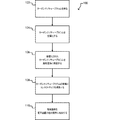
[0044] 図1は、本発明の幾つかの実施形態による、それぞれがカーボンナノチューブカラムを備えるプローブを有する接触器デバイスを含む電子装置を作成するためのプロセス100の例を示す。本明細書で使用する場合、カーボンナノチューブカラムは、一般的に垂直に位置合わせされたバンドル型カーボンナノチューブのグループを含むが、グループ内の幾つかのカーボンナノチューブは、重なり合う、織り合わさる、又は絡み合わさる、又はそうでなければ、1つ又は複数の場所で1つ又は複数の他のカーボンナノチューブと接触することができる。また、幾つかの実施形態では、カラム内のすべてのカーボンナノチューブがカラムの長さ全体に延在しているとは限らない。例えば、幾つかにラベル付けされた個々のカーボンナノチューブ216を含むカーボンナノチューブカラム214の例の写真を示す図2Cを参照されたい。 [0044] FIG. 1 illustrates an example of a process 100 for creating an electronic device that includes a contactor device having a probe, each comprising a carbon nanotube column, according to some embodiments of the present invention. As used herein, a carbon nanotube column typically includes a group of vertically aligned bundled carbon nanotubes, but some carbon nanotubes within the group overlap, interweave, or entangle. Or otherwise, it can contact one or more other carbon nanotubes at one or more locations. Also, in some embodiments, not all carbon nanotubes in the column extend the entire length of the column. For example, see FIG. 2C, which shows a photograph of an example of a carbon nanotube column 214 that includes several individually labeled individual carbon nanotubes 216.

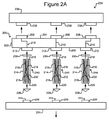
[0045] 図2Aは、本発明の幾つかの実施形態による、それぞれがカーボンナノチューブカラム214を備えるプローブ240を有する電子装置234が作成される図1のプロセス100の実施例を示す。図2Bは、アセンブルされた電子装置234を示す。図3〜図24は、図1のプロセス100の1つ又は複数のステップの例を示す。図3〜図24は、図1のプロセス100のうちの1つ又は複数のステップの例を示す。しかし、図3〜図24の例について説明する前に、以下のようにプロセス100の概要を述べる。 [0045] FIG. 2A illustrates an example of the process 100 of FIG. 1 in which an electronic device 234 is created having a probe 240, each comprising a carbon nanotube column 214, according to some embodiments of the present invention. FIG. 2B shows the assembled electronic device 234. 3-24 illustrate an example of one or more steps of the process 100 of FIG. 3-24 illustrate examples of one or more steps of the process 100 of FIG. However, before describing the example of FIGS. 3-24, an overview of the process 100 will be described as follows.

[0046] 図1に示すように、カーボンナノチューブカラムはステップ102で得ることができる。幾つかの実施形態では、カラムは図2Aに示すカラム214と同様とすることができる。上述のように、各カラム214は複数のバンドル型カーボンナノチューブ216を含むことができる。図2Aでは、各カラム214内にこのようなカーボンナノチューブ216が3つ示されているが、各カラム214は、より多くの(例えば、数十、数百、数千などの)個々のカーボンナノチューブ216を含むことができる。図2Aでは、3つのカーボンナノチューブカラム214が示されているが、図1のプロセス100のステップ102では、これより多くの又はこれより少ない数を得ることができる。図2Aに全体として示すように、カーボンナノチューブカラム214は、成長基板224上の成長材料226の表面222から成長できる。成長材料226は成長基板224上にあるため、たとえカーボンナノチューブカラム214が表面222上で直接成長する場合であっても、カーボンナノチューブカラム214は成長基板224上で成長すると言うことができる。カラム214の成長例については、図3を参照しながら以下で説明する。 As shown in FIG. 1, a carbon nanotube column can be obtained in step 102. In some embodiments, the column can be similar to the column 214 shown in FIG. 2A. As described above, each column 214 can include a plurality of bundle-type carbon nanotubes 216. In FIG. 2A, three such carbon nanotubes 216 are shown in each column 214, but each column 214 has more (eg, tens, hundreds, thousands, etc.) individual carbon nanotubes. 216 may be included. In FIG. 2A, three carbon nanotube columns 214 are shown, but more or less numbers can be obtained in step 102 of the process 100 of FIG. As shown generally in FIG. 2A, the carbon nanotube column 214 can be grown from the surface 222 of the growth material 226 on the growth substrate 224. Since the growth material 226 is on the growth substrate 224, it can be said that the carbon nanotube column 214 grows on the growth substrate 224 even if the carbon nanotube column 214 grows directly on the surface 222. An example of column 214 growth will be described below with reference to FIG.

[0047] 幾つかの実施形態では、カラム214はステップ102で、カラム214が移送される端子のパターンに対応するパターンで得ることができる。例えば図2Aに示す例では、カラム214はステップ102で得ることができ、カラム214が移送される配線基板202の端子212に対応するパターンで成長基板224に結合される。さらに、このパターンは、端子214を備えるプローブ240が接触するために使用される電子デバイスの端子に対応することができる。例えば、以下の図25及び図26についての説明から分かるように、カラム214は、ステップ102で、DUT2618をテストするためにカラム214が接触するために使用されるDUT2618(例えばテストの対象となる電子デバイス)の端子2616に対応するパターンで得ることができる。 [0047] In some embodiments, the column 214 may be obtained in step 102 in a pattern corresponding to the pattern of terminals to which the column 214 is transferred. For example, in the example shown in FIG. 2A, the column 214 can be obtained in step 102 and coupled to the growth substrate 224 in a pattern corresponding to the terminals 212 of the wiring substrate 202 to which the column 214 is transferred. Furthermore, this pattern can correspond to the terminals of the electronic device used for contacting the probe 240 with the terminals 214. For example, as can be seen from the description of FIGS. 25 and 26 below, the column 214 is a DUT 2618 that is used to contact the column 214 to test the DUT 2618 at step 102 (e.g., the electron under test). It can be obtained in a pattern corresponding to the terminal 2616 of the device.

[0048] 再度図1を参照すると、カラム214はステップ104で金属化することができる。本明細書で使用する場合、カラム214の金属化は、カラム214を備える少なくとも幾つかのカーボンナノチューブ216の少なくとも一部(例えば、幾つか、ほぼすべて、又はすべて)上での金属の堆積を含む。幾つかの実施形態では、金属材料232(例えば金、銀、銅、又は他の導電性材料)は、カラム214の内部にあるカーボンナノチューブ216の少なくとも幾つかの上で、各カラム214の内側に堆積できる。幾つかの実施形態では、金属材料232は、主に各カラム214の外側(例えば、カラム214の外側にあるカーボンナノチューブ216の少なくとも幾つか)上に堆積できる。幾つかの実施形態では、金属材料232は、各カラム214の外側上及び内側上に堆積できる。カラム214の内側での金属232の堆積の例については、図8及び図9に関して以下で説明し、カラム214の外側上の金属232の堆積の例については、図10A及び図10Bに関して以下で説明する。本明細書で使用する場合、カラム214の内側での金属化(又は金属材料232の堆積)とは、カラム214の内部にある少なくとも幾つかのカーボンナノチューブ216の少なくとも一部上での金属化(又は金属材料232の堆積)を意味し、カラム214の外側上での金属化(又は金属材料232の堆積)とは、カラム214の外側にある少なくとも幾つかのカーボンナノチューブ216の少なくとも一部(例えば、幾つか、ほぼすべて、又はすべて)の金属化(又はその上での金属材料232の堆積)を意味する。 [0048] Referring again to FIG. 1, the column 214 can be metallized at step 104. As used herein, metallization of column 214 includes metal deposition on at least some (eg, some, nearly all, or all) of at least some carbon nanotubes 216 comprising column 214. . In some embodiments, a metallic material 232 (eg, gold, silver, copper, or other conductive material) is placed inside each column 214 on at least some of the carbon nanotubes 216 inside the column 214. Can be deposited. In some embodiments, the metallic material 232 can be deposited primarily on the outside of each column 214 (eg, at least some of the carbon nanotubes 216 outside the column 214). In some embodiments, the metallic material 232 can be deposited on the outside and inside of each column 214. An example of metal 232 deposition inside column 214 is described below with respect to FIGS. 8 and 9, and an example of metal 232 deposition on the outside of column 214 is described below with respect to FIGS. 10A and 10B. To do. As used herein, metallization (or deposition of metal material 232) inside the column 214 refers to metallization (at least a portion of at least some of the carbon nanotubes 216 inside the column 214 ( Or metallization on the outside of the column 214 (or deposition of the metal material 232) means at least some of the at least some carbon nanotubes 216 outside the column 214 (e.g. , Some, almost all, or all) metallization (or deposition of metallic material 232 thereon).

[0049] 図1のステップ106では、金属化されたカーボンナノチューブカラム214を、図2Aに示すような配線基板202の導電性端子212に(例えばカップリング又は装着によって)移送することができる。上述のように、図2Aに示すカラム214は、成長基板224の成長材料226の表面222上で成長できるため、カラム214の端部220は、初期に、成長プロセスの結果として表面222に結合できる。図2A及び図2Bに示すように、カラム214の端部218は、カップリング230によって配線基板202の端子212に結合でき、カラム214の端部220は、成長材料226の表面222と(例えば機械的又は化学的手段によって)分離できる。成長基板224から配線基板202へのカラム214の移送の例については、図11〜図19に関して以下で説明する。端部218又は端部220のいずれかを第1の端部とみなすことができ、端部218又は端部220の他方を第2の反対端部とみなすことができる。 [0049] In step 106 of FIG. 1, the metallized carbon nanotube column 214 can be transferred (eg, by coupling or mounting) to a conductive terminal 212 of the wiring substrate 202 as shown in FIG. 2A. As described above, the column 214 shown in FIG. 2A can be grown on the surface 222 of the growth material 226 of the growth substrate 224 so that the end 220 of the column 214 can be initially bonded to the surface 222 as a result of the growth process. . As shown in FIGS. 2A and 2B, the end 218 of the column 214 can be coupled to the terminal 212 of the wiring substrate 202 by a coupling 230, and the end 220 of the column 214 can be coupled to the surface 222 of the growth material 226 (eg, mechanical Or by chemical means). An example of transferring the column 214 from the growth substrate 224 to the wiring substrate 202 is described below with respect to FIGS. Either end 218 or end 220 can be considered as a first end, and the other of end 218 or end 220 can be considered as a second opposite end.

[0050] 配線基板202は、端子212を備える任意の基板とすることができる。例えば、配線基板202は、プリント回路板、セラミック基板、又は端子212の支持に好適な他の同様の基板とすることができる。配線基板202のみ、又は他のコンポーネントとの組合せが、電子デバイス(図示せず)との圧力ベースの電気的接続を有効にするために十分な、カラム214を使用するための機械的支持を提供するので十分である。幾つかの実施形態では、配線基板202は、可撓性に対して十分に剛性であるものと考えることができる。図2Aに示すように、端子212は、配線基板202内及び/又は配線基板202上の電気接続210(例えば導電性ビア及び/又はトレース)によって、他の端子208に電気的に接続できる。図2Bに示すように、配線基板202の第1の側204上の端子208は、配線基板202の第2の側206上の端子212とは異なるピッチとすることができる。図2Bに示すように、端子208のピッチは端子212のピッチよりも大きいものとすることができる。 The wiring board 202 can be an arbitrary board provided with the terminals 212. For example, the wiring substrate 202 can be a printed circuit board, a ceramic substrate, or other similar substrate suitable for supporting the terminals 212. Wiring board 202 alone or in combination with other components provides mechanical support for using column 214 sufficient to enable pressure-based electrical connection with an electronic device (not shown). It is enough to do. In some embodiments, the wiring board 202 can be considered sufficiently rigid for flexibility. As shown in FIG. 2A, the terminal 212 can be electrically connected to other terminals 208 by electrical connections 210 (eg, conductive vias and / or traces) within and / or on the wiring board 202. As shown in FIG. 2B, the terminals 208 on the first side 204 of the wiring board 202 can be at a different pitch than the terminals 212 on the second side 206 of the wiring board 202. As shown in FIG. 2B, the pitch of the terminals 208 can be larger than the pitch of the terminals 212.

[0051] 図1のステップ108で、図2Aに示すように、コンタクトチップ228(導電性とすることができる)をカーボンナノチューブカラム214の端部220に提供することができる。例えば、コンタクトチップ228は、図2A及び図2Bに示すように、カラム214の端部220上に形成するか、又はこれに結合することができる。カラム214の端部220へのコンタクトチップ228の提供例については、図21A〜図25に関して以下で説明する。幾つかの実施形態では、コンタクトチップ228を含める必要はない。 [0051] Step 108 of FIG. 1 may provide a contact tip 228 (which may be conductive) to the end 220 of the carbon nanotube column 214, as shown in FIG. 2A. For example, the contact tip 228 can be formed on or coupled to the end 220 of the column 214 as shown in FIGS. 2A and 2B. Examples of providing contact tips 228 to the end 220 of the column 214 are described below with respect to FIGS. 21A-25. In some embodiments, the contact tip 228 need not be included.

[0052] 図1のステップ110で、ステップ106でのカラム214が移送される配線基板202を1つ又は複数の追加の要素に結合し、カラム214を電気プローブとすることができる電子装置を作成することができる。図2A及び図2Bは、電子装置234を形成するために配線基板202が電子コンポーネント236に結合される例を示す。図2Bは、配線基板202を電子コンポーネント236に結合する1つの方法を示しているが、他の結合方法も考えられる。電子装置234の導電性コンタクトプローブ240は、図2Bに示すようなカラム214を備えることができる。この例については、図26に関して以下で説明する。 [0052] Step 110 of FIG. 1 creates an electronic device that couples the wiring board 202 to which the column 214 in step 106 is transferred to one or more additional elements, making the column 214 an electrical probe. can do. 2A and 2B illustrate an example where the wiring board 202 is coupled to the electronic component 236 to form the electronic device 234. Although FIG. 2B illustrates one method for coupling the wiring board 202 to the electronic component 236, other coupling methods are also contemplated. The conductive contact probe 240 of the electronic device 234 can include a column 214 as shown in FIG. 2B. This example is described below with respect to FIG.

[0053] 図1のプロセス100の概要について述べてきたが、次に、プロセス100の各ステップの実施に対する例について、図3〜図24に関して説明する。 [0053] Having described the overview of the process 100 of FIG. 1, an example for the implementation of each step of the process 100 will now be described with respect to FIGS.

[0054] 上述のように、カーボンナノチューブカラム214は、図1のステップ102で、成長基板224上の成長材料226の表面222上にカラム214を成長させることによって得ることができる。図3は、内部でカーボンナノチューブカラム214が成長できる成長システム300を示す。便宜的及び説明がしやすいように、成長システム300に関しては、成長基板224の成長材料226の表面222上でのカラム214の成長に関して以下で説明するが、成長システム300はこれに限定されるものではなく、他の成長基板上で他のカーボンナノチューブカラムを成長させるために使用することもできる。 [0054] As described above, the carbon nanotube column 214 may be obtained by growing the column 214 on the surface 222 of the growth material 226 on the growth substrate 224 in step 102 of FIG. FIG. 3 shows a growth system 300 in which a carbon nanotube column 214 can grow. For convenience and ease of explanation, the growth system 300 will be described below with respect to the growth of the column 214 on the surface 222 of the growth material 226 of the growth substrate 224, although the growth system 300 is not limited thereto. Rather, it can be used to grow other carbon nanotube columns on other growth substrates.

[0055] 図3に示すように、成長システム300は、成長基板224を配置することができるチャンバ306(初期にはカラム214なし)を備えることができる。図に示すように、チャンバ306の温度(T)を制御するための温度制御デバイス302(例えばヒータ及び/又は冷却デバイス)が提供できる。また図に示すように、チャンバ306内への1つ又は複数の注入管308、316が提供でき、チャンバ306の外への1つ又は複数の排出管312が提供できる。(2つの注入管308、316及び1つの排出管312が示されているが、代替的に、より多くの又はより少ない注入管及び/又はより多くの排出管312を提供することもできる。)幾つかの実施形態では、図3に示すように、注入管316の端部314は、温度制御デバイス302の端部304から長さLだけチャンバ306内部に位置決めすることができる。 [0055] As shown in FIG. 3, the growth system 300 can include a chamber 306 (initially without a column 214) in which a growth substrate 224 can be placed. As shown, a temperature control device 302 (eg, a heater and / or cooling device) for controlling the temperature (T f ) of the chamber 306 can be provided. Also as shown, one or more injection tubes 308, 316 into the chamber 306 can be provided, and one or more drain tubes 312 out of the chamber 306 can be provided. (Two inlet tubes 308, 316 and one outlet tube 312 are shown, but more or fewer inlet tubes and / or more outlet tubes 312 may alternatively be provided.) In some embodiments, the end 314 of the injection tube 316 can be positioned within the chamber 306 by a length L from the end 304 of the temperature control device 302, as shown in FIG.

[0056] 成長溶液326をキャリアガス324内に導入するために、キャリアガス324との混合を高めるために成長溶液326を蒸発させることができる蒸発器318への入力付近又はその内部に注入デバイス322(例えばシリンジ又はポンプ)が提供できる。図に示すように、成長溶液326とキャリアガス324との混合物320は、蒸発器318から、注入管316を通してチャンバ306内へと送ることができる。この成長溶液326とキャリアガス324との混合物は、成長ガス320と呼ぶことができる。また図に示すように、幾つかの実施形態では、別のキャリアガス310を他の注入管308を通してチャンバ302内へ提供することもできる。別のキャリアガス310は、キャリアガス324と同じであるか又は異なるものとすることができる。ガス324及び310を供給するために、1つ又は複数のポンプ(図示せず)を提供できる。 [0056] An injection device 322 near or within the input to the evaporator 318, where the growth solution 326 can be evaporated to enhance mixing with the carrier gas 324 to introduce the growth solution 326 into the carrier gas 324. (Eg, a syringe or pump) can be provided. As shown, the mixture 320 of growth solution 326 and carrier gas 324 can be sent from the evaporator 318 through the inlet tube 316 and into the chamber 306. This mixture of growth solution 326 and carrier gas 324 can be referred to as growth gas 320. Also, as shown, in some embodiments, another carrier gas 310 can be provided into the chamber 302 through another injection tube 308. The other carrier gas 310 can be the same as or different from the carrier gas 324. One or more pumps (not shown) can be provided to supply gases 324 and 310.

[0057] 成長システム300は、以下のように使用できる。最初に、成長基板224を準備できる。成長基板224は、カラム214が成長する際にこのカラム214を支持するために好適な任意の構造とすることができる。好適な成長基板224の非限定的な例には、半導体ウェーハ、セラミック基板、有機材料を含む基板、無機材料を含む基板、又は、これらの任意の組合せが含まれる。成長材料226は、カーボンナノチューブカラム214が成長することが望ましい場所の基板224上に堆積させることができる。成長材料226の各堆積は、カーボンナノチューブカラム214の所望の断面形状でパターン化することができる。成長材料226は、任意の好適な方法でパターン化できる。例えば、成長材料226は、成長材料226の所望のパターンで基板224上に堆積できる。あるいは、成長材料226を基板224上に堆積した後、成長材料226の一部を選択的に除去し、成長材料226を所望のパターンで基板224上に残すこともできる。さらに他の代替方法として、成長材料226を基板224上に堆積した後、成長材料226の一部を選択的にカバーし、成長材料226を所望のパターンで露出させて基板224上に残すこともできる。さらに他の代替方法として、成長材料226を基板224上に堆積した後、成長材料226の一部をカバーし、次に、カバーの一部を選択的に除去して、成長材料226を所望のパターンで露出させて基板224上に残すこともできる。 [0057] The growth system 300 can be used as follows. Initially, a growth substrate 224 can be prepared. The growth substrate 224 can have any structure suitable for supporting the column 214 as it grows. Non-limiting examples of suitable growth substrates 224 include semiconductor wafers, ceramic substrates, substrates that include organic materials, substrates that include inorganic materials, or any combination thereof. Growth material 226 can be deposited on substrate 224 where it is desirable for carbon nanotube column 214 to grow. Each deposition of growth material 226 can be patterned with a desired cross-sectional shape of carbon nanotube column 214. The growth material 226 can be patterned in any suitable manner. For example, the growth material 226 can be deposited on the substrate 224 in a desired pattern of growth material 226. Alternatively, after the growth material 226 is deposited on the substrate 224, a portion of the growth material 226 can be selectively removed, leaving the growth material 226 on the substrate 224 in the desired pattern. As yet another alternative, after the growth material 226 is deposited on the substrate 224, a portion of the growth material 226 is selectively covered, leaving the growth material 226 exposed on the desired pattern on the substrate 224. it can. As yet another alternative, after the growth material 226 is deposited on the substrate 224, a portion of the growth material 226 is covered, and then a portion of the cover is selectively removed to remove the growth material 226 as desired It can also be exposed on the pattern and left on the substrate 224.

[0058] 成長材料226のパターン、又はより具体的に言えば、成長面222のパターンは、カラムの所望のパターンに対応することができる。上述のように、カラム214は、図1のプロセス100のステップ102で、カラム214が移送される端子のパターンに対応するパターンで得ることができる。例えば図2Aに示す例では、成長面226のパターン、したがって成長面226上で成長するカラム214のパターンは、カラム214が移送される配線基板202の端子212に対応することができる(図2を参照)。上述のように、そのパターンは、端子214を備えるプローブ240が接触のために使用される電子デバイスの端子に対応することができる。例えば、以下の図25及び図26についての説明から分かるように、成長材料226のパターン、したがって表面226上で成長するカラム214のパターンは、カラム214がDUT2618をテストするための接触に使用されるDUT2618(例えばテストの対象となる電子デバイス)の端子2616に対応することができる。上記内容は、カラム214が移送される電子デバイスのいずれかの端子に対応するパターン、及び/又は例えば、電子デバイスをテストするために電子デバイスとの電気接続を確立するためにカラム214によって接触される電子デバイスの端子に対応するパターンで、カラム214が得ることができる(例えば成長)方法の例である。 [0058] The pattern of growth material 226, or more specifically, the pattern of growth surface 222 can correspond to the desired pattern of the column. As described above, the columns 214 can be obtained in a pattern corresponding to the pattern of terminals to which the column 214 is transferred in step 102 of the process 100 of FIG. For example, in the example shown in FIG. 2A, the pattern of the growth surface 226, and hence the pattern of the column 214 grown on the growth surface 226, can correspond to the terminal 212 of the wiring substrate 202 to which the column 214 is transferred (see FIG. 2). reference). As described above, the pattern can correspond to the terminals of the electronic device on which the probe 240 with the terminals 214 is used for contact. For example, as can be seen from the description of FIGS. 25 and 26 below, the pattern of growth material 226, and hence the pattern of column 214 growing on surface 226, is used for contact by column 214 to test DUT 2618. It can correspond to the terminal 2616 of the DUT 2618 (for example, an electronic device to be tested). The above content is contacted by the column 214 to establish a pattern corresponding to any terminal of the electronic device to which the column 214 is transported and / or, for example, an electrical connection with the electronic device to test the electronic device. This is an example of how the column 214 can be obtained (eg, grown) in a pattern corresponding to the terminals of the electronic device.

[0059] 成長材料226は、成長溶液326に対して暴露された場合にその上にカーボンナノチューブが成長できる材料を含むか、又はそのような材料を含むように形成することができる表面222を有する任意の材料とすることができる。例えば成長材料226はシリコンを含むことができ、成長材料226の表面222は酸化膜を含むことができる。幾つかの実施形態では、成長基板224又は成長基板224の少なくとも上面は、成長面222などの成長面を有する成長材料224などの成長材料を含むことができ、この場合、成長材料224は成長基板224上に堆積される必要はない。このようなケースでは、成長基板224は成長材料226とすることができる。成長基板224が準備された後、成長基板224(カラム214なし)は、図3に示すようにチャンバ306内に配置できる。 [0059] Growth material 226 includes a surface 222 that can include, or can be formed to include, carbon nanotubes on which can be grown when exposed to growth solution 326. Any material can be used. For example, the growth material 226 can include silicon, and the surface 222 of the growth material 226 can include an oxide film. In some embodiments, the growth substrate 224 or at least the upper surface of the growth substrate 224 can include a growth material such as a growth material 224 having a growth surface such as the growth surface 222, where the growth material 224 is a growth substrate. There is no need to deposit on 224. In such a case, the growth substrate 224 can be the growth material 226. After the growth substrate 224 is prepared, the growth substrate 224 (without the column 214) can be placed in the chamber 306 as shown in FIG.

[0060] 温度制御デバイス302は、チャンバ306を所望の温度Tにするために利用できる。成長溶液326をキャリアガス324に導入し、蒸発器318及び注入管316を通してチャンバ306内へ、成長ガスとして提供することができる。蒸発器318は所望の温度T(例えば成長溶液326を蒸発させるのに十分な)に設定できる。成長溶液326をキャリアガス324に導入する際に、キャリアガス324は流量Qで提供でき、成長溶液326はポンプ量ζで提供できる。キャリアガス310も注入管308を通してチャンバ306内へ提供でき、キャリアガス310は流量Qで提供できる。 [0060] The temperature control device 302 may be utilized to bring the chamber 306 to the desired temperature Tf . Growth solution 326 can be introduced into carrier gas 324 and provided as growth gas into chamber 306 through evaporator 318 and injection tube 316. The evaporator 318 can be set to a desired temperature T e (eg, sufficient to evaporate the growth solution 326). When introducing growth solution 326 to carrier gas 324, the carrier gas 324 can be provided at a flow rate Q 1, the growth solution 326 can be provided in the pump volume zeta. The carrier gas 310 may be provided through the injection tube 308 into the chamber 306, the carrier gas 310 may be provided at a flow rate Q 2.

[0061] 成長溶液326の材料は、成長材料226の表面222上にカーボンナノチューブを成長させるために好適な任意の材料とすることができる。幾つかの実施形態では、成長溶液326はカーボンソース及び触媒を含むことができる。触媒は、表面222からカーボンナノチューブ216を成長させるために、カーボンソース内のカーボンを成長材料226の表面222と反応させる任意の材料とすることができる。好適な触媒の非限定的な例は、鉄有機金属材料(例えばフェロセン)である。他の好適な触媒の例には、ニッケル又はコバルト有機金属材料、酸化ジルコニウム、フェロセン酢酸、フェロセンアセトニトリル、フェロセンカルボキシアルデヒド、フェロセンカルボン酸、フェロセンジカルボキシアルデヒド、及びフェロセンジカルボン酸が含まれる。カーボンソースは、成長材料226の表面222上にカーボンナノチューブとして成長させるためのカーボンを提供する任意の材料とすることができる。好適なカーボンソースの非限定的な例は、液体炭化水素ソース(例えばキシレン)、芳香族炭化水素(例えば、ベンゼン、トルエン、キシレン、スチレン、エチルベンゼン及びすべてのアルキル化ベンゼン、シクロペンタジエン)、エチレン、及びメタンである。触媒又はカーボンソースがガスである場合、システム300は、触媒又はカーボンソースをガスとして収容するように修正できる。 [0061] The material of the growth solution 326 can be any material suitable for growing carbon nanotubes on the surface 222 of the growth material 226. In some embodiments, the growth solution 326 can include a carbon source and a catalyst. The catalyst can be any material that causes the carbon in the carbon source to react with the surface 222 of the growth material 226 to grow the carbon nanotubes 216 from the surface 222. Non-limiting examples of suitable catalysts are iron organometallic materials (eg ferrocene). Examples of other suitable catalysts include nickel or cobalt organometallic materials, zirconium oxide, ferroceneacetic acid, ferroceneacetonitrile, ferrocenecarboxaldehyde, ferrocenecarboxylic acid, ferrocenedicarboxaldehyde, and ferrocenedicarboxylic acid. The carbon source can be any material that provides carbon for growth as carbon nanotubes on the surface 222 of the growth material 226. Non-limiting examples of suitable carbon sources include liquid hydrocarbon sources (eg xylene), aromatic hydrocarbons (eg benzene, toluene, xylene, styrene, ethylbenzene and all alkylated benzenes, cyclopentadiene), ethylene, And methane. If the catalyst or carbon source is a gas, the system 300 can be modified to contain the catalyst or carbon source as a gas.

[0062] キャリアガス324の材料は、成長溶液326をチャンバ306内へ搬送するのに好適な任意のガスとすることができる。幾つかの実施形態では、キャリアガス324は、キャリア、サポートガス、及び空気を含むことができる。好適なキャリアの非限定的な例には、アルゴンガス又は窒素ガスが含まれ、好適なサポートガスの非限定的な例には、水素ガス(H)及び水蒸気が含まれる。キャリアガス310は、キャリアガス324と同じであるか又は異なるものとすることができる。上記材料は単なる例示としてのものであり、他の材料が成長溶液326及びキャリアガス310及び324を含むことができる。 [0062] The material of the carrier gas 324 can be any gas suitable for transporting the growth solution 326 into the chamber 306. In some embodiments, the carrier gas 324 can include a carrier, a support gas, and air. Non-limiting examples of suitable carriers include argon gas or nitrogen gas, and non-limiting examples of suitable support gases include hydrogen gas (H 2 ) and water vapor. The carrier gas 310 can be the same as or different from the carrier gas 324. The above materials are merely exemplary, and other materials can include growth solution 326 and carrier gases 310 and 324.

[0063] 成長溶液326及びキャリアガス310及び324を含む材料の濃度、チャンバ302及び蒸発器318のそれぞれの温度T及びT、成長溶液326のポンプ量ζ、キャリアガス326及び310の流量Q及びQ、温度制御デバイス306の端部304から注入管316の端部314までの長さL、成長材料226の表面222からカーボンナノチューブが成長する間の時間「t」、及び他のパラメータは、成長材料226の表面222上でカーボンナノチューブが成長するために望ましいように選択することができる。単に例示としてのものであり、上記内容には以下の値が好適であるが、これらに限定されるものではない。 [0063] The concentration of the material including the growth solution 326 and the carrier gases 310 and 324, the temperatures T f and T e of the chamber 302 and the evaporator 318, the pump amount ζ of the growth solution 326, and the flow rate Q of the carrier gases 326 and 310, respectively. 1 and Q 2 , the length L from the end 304 of the temperature control device 306 to the end 314 of the injection tube 316, the time “t” during which the carbon nanotubes grow from the surface 222 of the growth material 226, and other parameters Can be selected as desired for the growth of carbon nanotubes on the surface 222 of the growth material 226. The following values are suitable for the above contents, but are not limited to these examples.

キャリアガス310の組成:
/アルゴン比:0対0.5
キャリアガス324の組成:
/アルゴン比:0対0.5
空気:0〜20標準立方センチメートル/分(sccm)
成長溶液326の濃度:
キシレン中のフェロセンの濃度:0.0004〜0.05グラム/ミリリットル
チャンバ302の温度T:700〜850℃
蒸発器318の温度T:105〜250℃
成長溶液326のポンプ量ζ:2〜18ミリリットル/時(ml/h)
キャリアガス324の流量Q:50〜500sccm
キャリアガス310の流量Q:0〜200sccm
カーボンナノチューブの成長時間「t」:1〜180分
温度制御デバイス306の端部304から注入管316の端部314までの長さ「L」:8〜26センチメートル
[0064] 上記パラメータ及び他のパラメータはすべて、成長材料226の表面222から成長するカーボンナノチューブカラム214の機械的特徴に影響を与えることができる。このような機械的特徴の例は、一般に繰り返し可能な弾性範囲(以下「弾性範囲」と呼ぶ)、及びカラム214の剛性(例えば、フックの法則に従った、F*dであり、dは力Fに応答して移動する距離であり、*は乗算である、バネ定数「k」)を含むことができる。上記パラメータは、カラム214の端部220から端部218までの長さに沿って実質的に均一の機械的特徴を有するカラム214を得るために、カーボンナノチューブカラム214が成長する間、実質的に一定に維持することができる。あるいは、これらのパラメータのうちの1つ又は複数は、カラム214が成長する間、カラム214の端部220から端部218までの長さに沿ってカラムの上記機械的特徴(及び/又は他の機械的特徴)のうちの1つ又は複数を変更するために変更することができる。
Composition of carrier gas 310:
H 2 / argon ratio: 0 to 0.5
Composition of carrier gas 324:
H 2 / argon ratio: 0 to 0.5
Air: 0-20 standard cubic centimeters / minute (sccm)
Concentration of growth solution 326:
Concentration of ferrocene in xylene: 0.0004-0.05 grams / milliliter Temperature T f of chamber 302: 700-850 ° C.
Temperature T e of the evaporator 318: 105 to 250 ° C.
Pump amount of growth solution 326 ζ: 2 to 18 ml / hour (ml / h)
Flow rate Q 1 of carrier gas 324: 50 to 500 sccm
Flow rate Q 2 of carrier gas 310: 0 to 200 sccm
Carbon nanotube growth time “t”: 1-180 minutes Length “L” from end 304 of temperature control device 306 to end 314 of injection tube 316: 8-26 cm
[0064] All of the above parameters and other parameters can affect the mechanical characteristics of the carbon nanotube column 214 grown from the surface 222 of the growth material 226. Examples of such mechanical features are generally repeatable elastic range (hereinafter referred to as “elastic range”) and column 214 stiffness (eg, F * d, according to Hook's law, where d is the force The distance traveled in response to F, and * can include a spring constant “k”), which is a multiplication. The above parameters are substantially equal during the growth of the carbon nanotube column 214 to obtain a column 214 having substantially uniform mechanical characteristics along the length from end 220 to end 218 of the column 214. Can be kept constant. Alternatively, one or more of these parameters may affect the mechanical characteristics (and / or other) of the column along the length from the end 220 to the end 218 of the column 214 as the column 214 grows. Can be changed to change one or more of the mechanical features.

[0065] 例えば、カラム214が成長する間に、以下の表1に言及した(上述した)パラメータを変更することは、カラム214の機械的特徴に直接又は間接的に影響を与えることができるが、これに限定されるものではなく、
「直接」とは、パラメータの値の増加が機械的特徴の値の増加を引き起こし、パラメータの値の減少が機械的特徴の値の減少を引き起こす一方で、他のすべてのパラメータは変化しないことを意味し、
「間接的」とは、パラメータの値の増加が機械的特徴の値の減少を引き起こし、パラメータの値の減少が機械的特徴の値の増加を引き起こす一方で、他のすべてのパラメータは変化しないことを意味する。

Figure 0005796013
[0065] For example, while the column 214 is growing, changing the parameters mentioned in Table 1 below (described above) can directly or indirectly affect the mechanical characteristics of the column 214. , But is not limited to this,
“Direct” means that an increase in the value of a parameter causes an increase in the value of a mechanical feature, and a decrease in the value of a parameter causes a decrease in the value of a mechanical feature while all other parameters remain unchanged. Means
“Indirect” means that an increase in the value of a parameter causes a decrease in the value of a mechanical feature, and a decrease in the value of a parameter causes an increase in the value of a mechanical feature, while all other parameters remain unchanged Means.
Figure 0005796013


[0066] 図4Aは、カラム214の剛性に影響を与える上記で識別されたパラメータのうちの1つ又は複数が変化する間に、図3のシステム300で成長するカーボンナノチューブカラム214の例を示す。図4Aに示すように、カラム214は剛性領域402a、402b、及び402cと、軟質領域404a及び404bとを含む。3つの剛性領域402a、402b、及び402cと、2つの軟質領域404a及び404bとが示されているが、代替的に、カラム214の長さに沿って、より多くの又はより少ない剛性領域及び/又はより多くの又はより少ない軟質領域も形成できる。本明細書で使用する場合、軟質領域404a及び404bは、剛性領域402a、402b、及び402cの剛性よりも低い剛性を有する領域である。同様に、剛性領域402a、402b、及び402cは、軟質領域404a及び404bよりも高い剛性を有する領域である。

[0066] FIG. 4A shows an example of a carbon nanotube column 214 that grows in the system 300 of FIG. 3 while one or more of the above-identified parameters that affect the stiffness of the column 214 change. . As shown in FIG. 4A, the column 214 includes rigid regions 402a, 402b, and 402c and soft regions 404a and 404b. Although three rigid regions 402a, 402b, and 402c and two soft regions 404a and 404b are shown, alternatively, more or less rigid regions and / or along the length of column 214 Or more or fewer soft regions can be formed. As used herein, soft regions 404a and 404b are regions that have a lower stiffness than that of rigid regions 402a, 402b, and 402c. Similarly, the rigid regions 402a, 402b, and 402c are regions having higher rigidity than the soft regions 404a and 404b.

[0067] 図4Aに示すカラム214は、最初に第1の状態において剛性領域402cを上記パラメータで成長させること、次に、軟質領域404bが成長する間に、カラム214の剛性を低下させるために、パラメータのうちの1つ又は複数を第2の状態に変更すること(例えば、キャリアガス324の流量Qを増加すること、及び/又は成長溶液326のポンプ量ζを増加すること、及び/又は成長溶液326中の触媒の濃度を変更するためのメカニズム(例えば、触媒及びカーボンソースが注入デバイス322へ別々に導入される際に通ることのできる複数の入力ポート)が図3のシステム300内に提供された場合、成長溶液326中のフェロセンの濃度を低下させること)、次に、軟質領域404bが成長する間に、1つ又は複数のパラメータをそれらの初期値に戻すよう変更すること、次に、軟質領域404aが成長する間に、1つ又は複数のパラメータを第2の状態に変更すること、及び次に、剛性領域402aが成長する間に、1つ又は複数のパラメータをそれらの初期値に変更することによって成長させることができる。カーボンナノチューブ216、したがってカラム214は、最初に上端部218から成長することに留意されたい。すなわち最初に、端部218が成長材料224の表面222上に形成され、カラム214は端部218の下で成長する。したがって、例として図4Aに示すカラム214は、剛性領域402cが第1に表面222から成長し、次に軟質領域404bが剛性領域402cの下で表面222から成長し、次に剛性領域402bが軟質領域404bの下で表面222から成長し、次に軟質領域404aが剛性領域402bの下で表面222から成長し、次に剛性領域402aが軟質領域404aの下で表面222から成長する、というように成長する。カラム214の剛性に影響を与える1つ又は複数のパラメータにおける変更のタイミングを適切に決定することによって、剛性領域402a、402b、及び402cと、軟質領域404a及び404bとのサイズ及び位置を選択することができる。例えば、剛性領域402a、402b、及び402cと、軟質領域404a及び404bとを端部220から端部218までのカラム214の長さに沿った所定の位置に配置することができる。 [0067] The column 214 shown in FIG. 4A is used to first grow the rigid region 402c with the above parameters in the first state, and then to reduce the stiffness of the column 214 while the soft region 404b is growing. Changing one or more of the parameters to a second state (eg, increasing the flow rate Q 1 of the carrier gas 324 and / or increasing the pumping amount ζ of the growth solution 326, and / or Or a mechanism for changing the concentration of the catalyst in the growth solution 326 (eg, multiple input ports through which the catalyst and carbon source can be separately introduced into the injection device 322) is within the system 300 of FIG. Reducing the concentration of ferrocene in the growth solution 326), then one or more parameters while the soft region 404b is growing. Changing the parameters back to their initial values, then changing one or more parameters to the second state while the soft region 404a is growing, and then the rigid region 402a is growing In the meantime, it can be grown by changing one or more parameters to their initial values. Note that the carbon nanotubes 216, and thus the column 214, initially grow from the top end 218. That is, first, an end 218 is formed on the surface 222 of the growth material 224 and the column 214 grows under the end 218. Thus, for example, column 214 shown in FIG. 4A has rigid region 402c first growing from surface 222, then soft region 404b growing from surface 222 below rigid region 402c, and then rigid region 402b is soft. Grow from surface 222 under region 404b, then soft region 404a grows from surface 222 under rigid region 402b, then rigid region 402a grows from surface 222 under soft region 404a, etc. grow up. Selecting the size and position of the rigid regions 402a, 402b, and 402c and the soft regions 404a and 404b by appropriately determining the timing of changes in one or more parameters that affect the stiffness of the column 214. Can do. For example, the rigid regions 402a, 402b, and 402c and the soft regions 404a and 404b can be placed at predetermined locations along the length of the column 214 from the end 220 to the end 218.

[0068] 図4Bは、基板224上に交互の剛性領域462及び軟質領域464を有するカーボンナノチューブカラム214の例を示す写真である。図4Bを見れば分かるように、軟質領域464は濃いリングに見える。剛性領域462は、図4Aの剛性領域402a、402b、及び402cの例とすることができ、軟質領域464は、図4Aの軟質領域404a及び404bの例とすることができる。もちろん、図4Bに示されるよりも多いか又は少ない剛性領域462及び/又は多いか又は少ない軟質領域464が存在しても良い。 FIG. 4B is a photograph showing an example of a carbon nanotube column 214 having alternating rigid regions 462 and soft regions 464 on a substrate 224. As can be seen from FIG. 4B, the soft region 464 appears as a dark ring. The rigid region 462 can be an example of the rigid regions 402a, 402b, and 402c of FIG. 4A, and the soft region 464 can be an example of the soft regions 404a and 404b of FIG. 4A. Of course, there may be more or less rigid regions 462 and / or more or less soft regions 464 than shown in FIG. 4B.

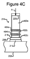
[0069] 図4Cは、カラムが(上述のように)配線基板202に移送された後の図4Aのカラム214を示す。図4Cに示すように、力Fをカラムの端部220に印加することにより、軟質領域404a及び404bを座屈させることができる。これは、軟質領域404a及び404bの剛性が、剛性領域402a、402b、及び402cよりも低いことによる。端部220上の力Fに対するカラム214の反応、したがってカラム214の機械的特性(例えば、カラム214の剛性、弾性範囲、及び/又は他の機械的特徴)は、カラム214の長さに沿った1つ又は複数の軟質領域404a及び/又は404bの選択的形成によってカスタマイズすることができる。 [0069] FIG. 4C shows the column 214 of FIG. 4A after the column has been transferred to the wiring board 202 (as described above). As shown in FIG. 4C, the soft regions 404a and 404b can be buckled by applying a force F to the end 220 of the column. This is because the stiffness of the soft regions 404a and 404b is lower than that of the rigid regions 402a, 402b, and 402c. The response of the column 214 to the force F on the end 220, and thus the mechanical properties of the column 214 (eg, the stiffness, elastic range, and / or other mechanical characteristics of the column 214) are along the length of the column 214. It can be customized by selective formation of one or more soft regions 404a and / or 404b.

[0070] 図4Aに示す例では、カラム214の剛性に影響を与える1つ又は複数のパラメータは2つの状態間で変更されるものとして説明されたため、結果として、剛性領域402a、402b、及び402cが実質的に同じ剛性を有し、軟質領域404a及び404bが(剛性領域402a、402b、及び402cの剛性よりも低い)実質的に同じ剛性を有する。しかし、これは単なる例示としてのものであり、多くの変形が可能である。図5〜図7は、このような変形の非限定的な例を示す。 [0070] In the example shown in FIG. 4A, one or more parameters affecting the stiffness of column 214 have been described as being changed between two states, resulting in stiffness regions 402a, 402b, and 402c. Have substantially the same stiffness, and the soft regions 404a and 404b have substantially the same stiffness (lower than the stiffness of the rigid regions 402a, 402b, and 402c). However, this is merely an example and many variations are possible. 5-7 show non-limiting examples of such variations.

[0071] 図5Aでは、剛性に影響を与える1つ又は複数のパラメータは、初期の値から始まり、カラム214が成長するにつれて、端部220から端部218までのカラム214の剛性を(所望に応じて)増加又は減少させるために、漸次変更することができる。したがってカラム214は、端部220から端部218までカラム214の長さに沿って増加又は減少する剛性勾配Gを有することができる。例えば、端部220から端部218へと剛性を増加させる剛性勾配Gでカラム214を成長させるために、カラム214が成長する間に、キャリアガス324の流量Qを漸次増加させる、及び/又は成長溶液326のポンプ量ζを漸次増加させる、及び/又は図3のシステム300内に成長溶液326中の触媒の濃度を変えるためのメカニズム(例えば、触媒及びカーボンソースが注入デバイス322へ別々に導入される際に通ることのできる複数の入力ポート)が提供されている場合、成長溶液326中のフェロセンの濃度を漸次減少させるといった上記パラメータのうちの1つ又は複数を以下のように変更することができる。カラムが成長するにつれてカラム214の剛性を変更するように、変化する1つ又は複数のパラメータの初期値を選択することによって、端部218でのカラム214の剛性値を所望の値にすることができる。同様に、カラムが成長するにつれてカラム214の剛性を変化させるように、変化する1つ又は複数のパラメータの変化率及び最終値を選択することによって、カラム214の長さに沿った剛性の変化率及び端部220でのカラムの剛性値を所望の値にすることができる。図5Bは、カラム214が成長するにつれて流量Qが経時的に増加する例を示し、これは事実上、流量Qが成長位置「z」(すなわち、カラム214が表面222から成長する際の端部218の位置)の関数として増加し、結果として、図5Aに示すように、カラム214の長さに沿った剛性勾配Gの増加を生じさせることを意味する。 [0071] In FIG. 5A, the one or more parameters that affect the stiffness start with initial values and, as the column 214 grows, the stiffness of the column 214 from end 220 to end 218 (as desired). It can be changed gradually to increase or decrease (accordingly). Thus, the column 214 can have a stiffness gradient G that increases or decreases along the length of the column 214 from the end 220 to the end 218. For example, in order to grow the column 214 with rigid gradient G to increase the rigidity and from the end 220 to end 218, while the column 214 is grown, gradually increasing the flow rate to Q 1 carrier gas 324, and / or A mechanism for gradually increasing the pumping amount ζ of the growth solution 326 and / or changing the concentration of the catalyst in the growth solution 326 within the system 300 of FIG. 3 (eg, catalyst and carbon source are separately introduced into the injection device 322. Change one or more of the above parameters to gradually reduce the concentration of ferrocene in the growth solution 326 as follows: Can do. By selecting an initial value for one or more parameters that change so as to change the stiffness of the column 214 as the column grows, the stiffness value of the column 214 at the end 218 may be brought to a desired value. it can. Similarly, the rate of change of stiffness along the length of column 214 by selecting the rate of change and final value of one or more parameters to change so that the stiffness of column 214 changes as the column grows. And the stiffness value of the column at the end 220 can be set to a desired value. FIG. 5B shows an example in which the flow rate Q 1 increases over time as the column 214 grows, which effectively causes the flow rate Q 1 to grow at the growth position “z” (ie, as the column 214 grows from the surface 222. Means an increase in stiffness gradient G along the length of the column 214, as shown in FIG. 5A.

[0072] 図6は、図5Aのカラム214の変化を示す。図6のカラム214は、2つの領域602及び604を含む。領域604は、端部220から領域602との接合部606へと増加する、剛性勾配Gを有する。領域602は、カラム214の接合部606から端部218へと減少する剛性勾配Gを有する。例えば、図6のカラム214を成長させるために、カラム214が端部218から接合部606へと成長するにつれて、キャリアガス324の流量Q及び/又は成長溶液326のポンプ量ζを漸次減少でき、カラム214が接合部606から端部220へと成長するにつれて、キャリアガス324の流量Q及び/又は成長溶液326のポンプ量ζを漸次増加できるというように、上記パラメータのうちの1つ又は複数を変更することができる。代替的に又は追加的に、図3のシステム300内に成長溶液326中の触媒の濃度を変えるためのメカニズム(例えば、触媒及びカーボンソースが注入デバイス322へ別々に導入される際に通ることのできる複数の入力ポート)が提供された場合、端部218から接合部606へとカラムが成長するにつれて、成長溶液326中のフェロセンの濃度を漸次増加させることができ、接合部606から端部220へとカラム214が成長するにつれて、成長溶液326中のフェロセンの濃度を漸次減少させることができる。図6には、それぞれ異なる剛性勾配を有する2つの領域602及び604が示されているが、カラム214は3つ以上のこのような領域を有することができる。 [0072] FIG. 6 illustrates a change in column 214 of FIG. 5A. Column 214 of FIG. 6 includes two regions 602 and 604. Region 604 has a stiffness gradient G 2 that increases from end 220 to junction 606 with region 602. Region 602 has a stiffness gradient G 1 that decreases from junction 606 to end 218 of column 214. For example, in order to grow the column 214 of FIG. 6, as the column 214 is grown to a junction 606 from the end 218, you can gradually reduce the pumping rate ζ of the flow Q 1 and / or growth solution 326 of carrier gas 324 , as column 214 is grown to the end 220 from the junction 606, so that the pumping rate ζ of the flow Q 1 and / or growth solution 326 of carrier gas 324 can be increased gradually, one of the above parameters or Multiple can be changed. Alternatively or additionally, a mechanism for changing the concentration of the catalyst in the growth solution 326 within the system 300 of FIG. 3 (e.g., passing when the catalyst and carbon source are separately introduced into the injection device 322). As the column grows from the end 218 to the junction 606, the concentration of ferrocene in the growth solution 326 can be increased progressively from the junction 606 to the end 220. As the column 214 grows, the concentration of ferrocene in the growth solution 326 can be gradually reduced. Although two regions 602 and 604, each having a different stiffness gradient, are shown in FIG. 6, the column 214 can have more than two such regions.

[0073] 図7は、図4Aに示すカラム214の変化の別の例を示す。図7のカラム214は、領域702、704、706、及び708を含み、そのうちの少なくとも3つは異なる剛性値を有することができる。実際に、領域702、704、706、及び708のそれぞれが、異なる剛性を有することができる。例えば図7に示すカラム214は、最初にキャリアガス324の流量Q及び/又は成長溶液326のポンプ量ζ及び/又は領域702の所望の剛性を生成する値を有する成長溶液326中のフェロセンの濃度で、領域702を成長させること、次に、(成長溶液326中の触媒の濃度を変更するためのメカニズム(例えば、触媒及びカーボンソースが注入デバイス322へ別々に導入される際に通ることのできる複数の入力ポート)が図3のシステム300内に提供された場合)キャリアガス324の流量Q及び/又は成長溶液326のポンプ量ζ及び/又は成長溶液326中のフェロセンの濃度のうちの少なくとも1つを領域704の所望の剛性(領域702の剛性とは異なり得る)を生成する値に変更すること、次に、(成長溶液326中の触媒の濃度を変更するためのメカニズム(例えば、触媒及びカーボンソースが注入デバイス322へ別々に導入される際に通ることのできる複数の入力ポート)が図3のシステム300内に提供された場合)キャリアガス324の流量Q及び/又は成長溶液326のポンプ量ζ及び/又は成長溶液326中のフェロセンの濃度のうちの少なくとも1つを領域706の所望の剛性(領域702及び領域704の剛性とは異なり得る)を生成する値に変更すること、次に、(成長溶液326中の触媒の濃度を変更するためのメカニズム(例えば、触媒及びカーボンソースが注入デバイス322へ別々に導入される際に通ることのできる複数の入力ポート)が図3のシステム300内に提供された場合)キャリアガス324の流量Q及び/又は成長溶液326のポンプ量ζ及び/又は成長溶液326中のフェロセンの濃度のうちの少なくとも1つを領域708の所望の剛性(領域702、領域704、及び領域706の剛性とは異なり得る)を生成する値に変更することによって成長させることができる。図7には4つの異なる領域702、704、706、及び708が示されているが、より多くの又はより少ないこのような領域が存在することができ、それらのうちの幾つか又はすべてが異なる剛性値を有することができる。 [0073] FIG. 7 shows another example of a change in the column 214 shown in FIG. 4A. Column 214 of FIG. 7 includes regions 702, 704, 706, and 708, at least three of which can have different stiffness values. Indeed, each of regions 702, 704, 706, and 708 can have a different stiffness. For example, the column 214 shown in FIG. 7 may initially include the flow rate Q 1 of the carrier gas 324 and / or the pump amount ζ of the growth solution 326 and / or the value of ferrocene in the growth solution 326 having values that produce the desired stiffness of the region 702. Growing the region 702 at a concentration, then (a mechanism for changing the concentration of the catalyst in the growth solution 326 (eg, passing through the catalyst and carbon source as they are introduced separately into the injection device 322) A plurality of possible input ports) provided in the system 300 of FIG. 3) of the carrier gas 324 flow rate Q 1 and / or the growth solution 326 pump amount ζ and / or the concentration of ferrocene in the growth solution 326. Changing at least one to a value that produces the desired stiffness of region 704 (which may be different from the stiffness of region 702); A mechanism for changing the concentration of catalyst in 6 (eg, multiple input ports through which the catalyst and carbon source can be introduced separately into the injection device 322) is provided in the system 300 of FIG. At least one of the flow rate Q 1 of the carrier gas 324 and / or the pump amount ζ of the growth solution 326 and / or the concentration of ferrocene in the growth solution 326 is set to the desired stiffness (region 702 and region 704). Change to a value that produces (which may differ from the stiffness of the catalyst), and then a mechanism for changing the concentration of the catalyst in the growth solution 326 (eg, the catalyst and carbon source are introduced separately to the injection device 322). that a plurality of input ports which can be through which) may have been provided in the system 300 of FIG. 3) of the carrier gas 324 flow rate Q 1及And / or at least one of the pumping amount ζ of the growth solution 326 and / or the concentration of ferrocene in the growth solution 326 may be a desired stiffness of the region 708 (which may be different from the stiffness of the regions 702, 704, and 706) Can be grown by changing the value to generate. Although four different regions 702, 704, 706, and 708 are shown in FIG. 7, there can be more or fewer such regions, some or all of which are different It can have a stiffness value.

[0074] 図4A及び図5〜図7に示す例は、網羅的又は限定的なものではなく、多くの変形が可能である。例えば、図4A及び図5〜図7の例では機械的特性剛性は変化するが、他の機械的特性に影響を与える上記表1のパラメータのうちの1つ又は複数を変更することによって、カラム214が成長する間に、カラム214の他の機械的特性を変更することができる。例えば、(カラム214の剛性ではなく、又はこれに加えて)カラム214の弾性範囲は、弾性範囲に影響を与えるパラメータ(例えば、キャリアガス310中のアルゴン/Hの比、成長溶液326中のフェロセンの濃度、成長溶液326のポンプ量ζ、又は温度制御デバイス306の端部304から注入管316の端部314までの長さL)のうちの1つ又は複数を変更することによって変更することができる。例えば、図4Aの領域402a、402b、及び403は、領域404a及び404bと比較して異なる弾性範囲を有することができる。同様に、図5Aのカラム214の勾配G及び/又は図6のカラム214の領域602及び604の勾配G及びGは、変化する剛性値ではなく、又はこれに加えて、変化する弾性範囲値を有することができる。同様に、図7のカラム214の領域702、704、706、及び708は、異なる剛性値を有するのではなく、又はこれに加えて、異なる弾性範囲値を有することができる。同様に、図8のカラム214の領域802、804、806、及び808は、異なる剛性値を有するのではなく、又はこれに加えて、異なる弾性範囲値を有することができる。 [0074] The examples shown in FIGS. 4A and 5 to 7 are not exhaustive or restrictive, and many variations are possible. For example, in the examples of FIGS. 4A and 5-7, the mechanical property stiffness varies, but by changing one or more of the parameters in Table 1 above that affect other mechanical properties, the column While 214 grows, other mechanical properties of column 214 can be changed. For example, the elastic range of column 214 (rather than or in addition to column 214 stiffness) is a parameter that affects the elastic range (eg, the ratio of argon / H 2 in carrier gas 310, growth solution 326 Changing by changing one or more of the ferrocene concentration, the pumping amount ζ of the growth solution 326, or the length L) from the end 304 of the temperature control device 306 to the end 314 of the injection tube 316 Can do. For example, regions 402a, 402b, and 403 in FIG. 4A can have different elastic ranges compared to regions 404a and 404b. Similarly, the slope G of column 214 of FIG. 5A and / or the slopes G 1 and G 2 of regions 602 and 604 of column 214 of FIG. 6 are not variable stiffness values, or in addition, vary elastic range. Can have a value. Similarly, regions 702, 704, 706, and 708 of column 214 in FIG. 7 may have different elastic range values, rather than or in addition to having different stiffness values. Similarly, regions 802, 804, 806, and 808 of column 214 of FIG. 8 may have different elastic range values, rather than or in addition to having different stiffness values.

[0075] 再度図1のプロセス100を参照すると、上述のように図3〜図7のうちの1つ又は複数でカラム214を成長させることによって、102でカーボンナノチューブカラム214を提供できる。さらに、カラム214は、図4A及び図5〜図7に示す例で示すように、変化する剛性値などの変化する機械的特徴を有するように成長させることができる。あるいは、カラム214は他の方法で得ることができる。例えば成長基板224は、成長材料226からすでに成長したカラム214を用いて得ることができる。 [0075] Referring again to the process 100 of FIG. 1, a carbon nanotube column 214 can be provided at 102 by growing the column 214 in one or more of FIGS. 3-7 as described above. Further, the column 214 can be grown to have varying mechanical characteristics, such as varying stiffness values, as shown in the examples shown in FIGS. 4A and 5-7. Alternatively, the column 214 can be obtained in other ways. For example, the growth substrate 224 can be obtained using a column 214 already grown from the growth material 226.

[0076] ステップ102でカラム214がどのように得られるかにかかわらず、ステップ104でカーボンナノチューブカラム214を金属化することができる。あるいは、カラム214は、ステップ106でカラムの移送後に金属化することができる。カラム214がいつ金属化されるかにかかわらず、カラム214は、例えばカラム214の導電性及び/又は通電能力を上昇させるために金属化することができる。例えばカラム214は、テストの対象となる電子デバイス(例えば半導体ダイ)との圧力ベースの電気的接触を確立するためにカラム214に対して使用されるのに十分なように、カラム214の導電性及び/又は通電能力を上昇させるために金属化することができる。カーボンナノチューブカラム214の金属化は、カラム214の内側の少なくとも幾つかのカーボンナノチューブ216上にカラム214の内側で金属232を堆積させること、及び/又はカラム214の外側の少なくとも幾つかのカーボンナノチューブ216上にカラム214の外側で金属232を堆積させることを含むことができる。金属232の任意の好適な堆積方法を使用できる。例えば金属232は、スパッタリング、化学蒸着、無電解めっき、電気めっき、又は他の同様の堆積方法によって、カラム214上に堆積させることができる。上述のように、カラム214上への金属堆積とは、カラム214を形成する少なくとも幾つかのカーボンナノチューブ216の少なくとも一部上への金属堆積を意味する。幾つかの実施形態では、幾つか、ほぼすべて、又はすべてのカーボンナノチューブ216を金属化することができる。 [0076] Regardless of how column 214 is obtained in step 102, carbon nanotube column 214 may be metallized in step 104. Alternatively, column 214 can be metallized after column transfer at step 106. Regardless of when column 214 is metallized, column 214 can be metallized, for example, to increase the conductivity and / or current carrying capacity of column 214. For example, the conductivity of the column 214 is sufficient so that the column 214 is sufficient for use with the column 214 to establish pressure-based electrical contact with the electronic device under test (eg, a semiconductor die). And / or can be metallized to increase current carrying capacity. Metallization of the carbon nanotube column 214 may include depositing metal 232 inside the column 214 on at least some carbon nanotubes 216 inside the column 214 and / or at least some carbon nanotubes 216 outside the column 214. Depositing metal 232 on the outside of column 214 may be included. Any suitable deposition method of metal 232 can be used. For example, the metal 232 can be deposited on the column 214 by sputtering, chemical vapor deposition, electroless plating, electroplating, or other similar deposition methods. As described above, metal deposition on the column 214 means metal deposition on at least some of the at least some carbon nanotubes 216 that form the column 214. In some embodiments, some, nearly all, or all of the carbon nanotubes 216 can be metallized.

[0077] カラムの内側のカーボンナノチューブ216上に金属232を堆積させる方法は、ある実施形態では有利であるが、本発明はこれに限定されるものではない。図8は金属化システム800を示し、図9は、カラム214の内側でカーボンナノチューブ216上に金属232を堆積させることができる図1のステップ102で得られたカラム214を金属化するためのシステム800の使用プロセスを示す。 [0077] Although the method of depositing the metal 232 on the carbon nanotubes 216 inside the column is advantageous in certain embodiments, the present invention is not so limited. FIG. 8 shows a metallization system 800 and FIG. 9 shows a system for metallizing the column 214 obtained in step 102 of FIG. 1 where metal 232 can be deposited on the carbon nanotubes 216 inside the column 214. 800 usage processes are shown.

[0078] 図8に示すように、金属化システム800は、チャンバ802と、チャンバ802内の温度を制御可能な温度制御デバイス804(例えば、さらにヒータ及び/又は冷却デバイス)とを備えることができる。温度制御デバイス804は誘導ヒータを備えることができ、チャンバは非導電性とすることができる。例えば、チャンバ802はガラス板を備えることができる。1つ又は複数の注入ポート806及び810(2つが示されているが、より少ないか又はより多く含むことができる)は、チャンバ802内に材料(ガス808及び812)を導入することができる手段を提供することができる。システム800は、チャンバ802を排気することができる真空ポンプ814を含むこともできる。 [0078] As shown in FIG. 8, the metallization system 800 can include a chamber 802 and a temperature control device 804 (eg, further a heater and / or cooling device) that can control the temperature in the chamber 802. . The temperature control device 804 can comprise an induction heater and the chamber can be non-conductive. For example, the chamber 802 can comprise a glass plate. One or more injection ports 806 and 810 (two are shown but may include fewer or more) means by which material (gas 808 and 812) may be introduced into chamber 802. Can be provided. System 800 can also include a vacuum pump 814 that can evacuate chamber 802.

[0079] 図9のステップ902で、図8のシステム800を使用して、図8に示すように、第1に成長基板224をチャンバ802内に配置することによって、カーボンナノチューブカラム214を金属化することができる。図9のステップ904では、図8に示すように、注入ポート806を通してチャンバ802内に前駆体ガス808を導入することができる。前駆体ガス808は、カラム214の内側でカーボンナノチューブ216上に堆積される金属232を含むことができる。幾つかの実施形態では、前駆体ガス808は、化学蒸着ガス(CVD)及び金属(例えば金、銀、プラチナ、銅、パラジウム、タングステン、又は同様の金属)を含むことができる。例えば、前駆体ガス808及び金属は、マサチューセッツ州ニューベリーポートのStrem Chemicals,Inc.から入手可能な、ジメチル(アセチルアセトナート)金(III)、ジメチル(トリフルオロアセチルアセトナート)金(III)、クロロ(トリメチルホスフィン)金、クロロ(トリエチルホスフィン)金、トリメチル(トリメチルホスフィン)金、又はメチル(トリメチルホスフィン)金のうちのいずれかを含むことができる。前駆体ガス808は、前駆体ガス808をカラム214に通し、カラム214に侵入させるのに十分な圧力の下でチャンバ802に導入することができる。これを実行する1つの非限定的な方法は、真空ポンプ814を使用してチャンバ802を排気し、大気圧よりわずかに高い圧力から大気圧の約10倍までの間の圧力の下で、注入ポート806を通して前駆体ガス808を導入するものである。上記圧力範囲は単なる例示としてのものであり、本発明はこれに限定されるものではない。誘導加温に加えて、フラッシュランプ又は半導体ウェーハの迅速な温度処理用に開発された他の技術を使用する放射加熱も使用できる。 [0079] Step 902 of FIG. 9 uses the system 800 of FIG. 8 to first metallize the carbon nanotube column 214 by placing a growth substrate 224 in the chamber 802 as shown in FIG. can do. In step 904 of FIG. 9, precursor gas 808 may be introduced into chamber 802 through injection port 806, as shown in FIG. The precursor gas 808 may include a metal 232 that is deposited on the carbon nanotubes 216 inside the column 214. In some embodiments, the precursor gas 808 can include a chemical vapor deposition (CVD) and a metal (eg, gold, silver, platinum, copper, palladium, tungsten, or similar metal). For example, precursor gas 808 and metal are available from Strem Chemicals, Inc. of Newburyport, Massachusetts. Dimethyl (acetylacetonato) gold (III), dimethyl (trifluoroacetylacetonato) gold (III), chloro (trimethylphosphine) gold, chloro (triethylphosphine) gold, trimethyl (trimethylphosphine) gold, available from Or methyl (trimethylphosphine) gold. Precursor gas 808 can be introduced into chamber 802 under sufficient pressure to pass precursor gas 808 through column 214 and into column 214. One non-limiting way to do this is to evacuate chamber 802 using vacuum pump 814 and inject under a pressure between slightly above atmospheric pressure and about 10 times atmospheric pressure. The precursor gas 808 is introduced through the port 806. The above pressure range is merely an example, and the present invention is not limited to this. In addition to induction heating, radiant heating using flash lamps or other techniques developed for rapid temperature processing of semiconductor wafers can also be used.

[0080] 図9のステップ906で、チャンバ802は、フラッシングガスでフラッシュすることができる。例えばフラッシングガス812は、注入ポート810を通してチャンバ802内に導入し、真空ポンプ814によってチャンバ802から除去することができる。フラッシングガス812は、カラム214のカーボンナノチューブ216とはっきりと反応することのないガスとすることができる。好適なフラッシングガス812の例は、窒素(N)を含むことができる。 [0080] At step 906 of FIG. 9, the chamber 802 may be flushed with a flushing gas. For example, flushing gas 812 can be introduced into chamber 802 through injection port 810 and removed from chamber 802 by vacuum pump 814. The flushing gas 812 can be a gas that does not react clearly with the carbon nanotubes 216 of the column 214. An example of a suitable flushing gas 812 can include nitrogen (N 2 ).

[0081] フラッシングガス812をチャンバ802に導入し、真空ポンプ814によって、前駆体ガス808の一部がカラム214内側のカーボンナノチューブ216周囲に残存するように、前駆体ガス808の拡散速度よりも十分に低い速度でチャンバ802から除去することができる。すなわち、フラッシングガス812をチャンバ802に導入し、カラム214の内側で、所望の量の前駆体ガス808をカラム214内側のカーボンナノチューブ216周囲に残存させ、またオプションで、チャンバ802内のカラム214の外側に前駆体ガス808の一部を残存させながら、チャンバ内の前駆体ガスをチャンバ802の外にフラッシュさせることができる。カラム214の内側及びチャンバ802内のカラム214の周囲(したがってカラム214の外側)に残る前駆体ガス808の量は、前駆体ガス808の拡散速度と比較してチャンバ802の内部及び外部へのフラッシングガス812の導入速度を制御すること、及びステップ908の開始(以下で説明)によって制御できる。図を見れば分かるように、カラム214内に残る前駆体ガス808の量は、カラム214の内側(すなわち、カラム214内側のカーボンナノチューブ216上)に堆積する金属232の量に対応でき、チャンバ802内のカラム214の外側周囲に残る前駆体ガス808の量は、カラム214の外側(すなわち、カラム214外側のカーボンナノチューブ216上)に堆積する金属232の量に対応することができる。 [0081] The flashing gas 812 is introduced into the chamber 802, and the diffusion rate of the precursor gas 808 is sufficiently higher so that a part of the precursor gas 808 remains around the carbon nanotubes 216 inside the column 214 by the vacuum pump 814. Can be removed from the chamber 802 at a very low rate. That is, the flushing gas 812 is introduced into the chamber 802, leaving the desired amount of precursor gas 808 around the carbon nanotubes 216 inside the column 214 inside the column 214, and optionally, the column 214 in the chamber 802. The precursor gas in the chamber can be flushed out of the chamber 802 while leaving a portion of the precursor gas 808 on the outside. The amount of precursor gas 808 remaining inside column 214 and around column 214 in chamber 802 (and thus outside column 214) is flushed into and out of chamber 802 as compared to the diffusion rate of precursor gas 808. It can be controlled by controlling the rate of introduction of gas 812 and the start of step 908 (described below). As can be seen, the amount of precursor gas 808 remaining in the column 214 can correspond to the amount of metal 232 deposited inside the column 214 (ie, on the carbon nanotubes 216 inside the column 214), and chamber 802. The amount of precursor gas 808 remaining around the outside of the inner column 214 can correspond to the amount of metal 232 deposited on the outside of the column 214 (ie, on the carbon nanotubes 216 outside the column 214).

[0082] 図のステップ908で、温度制御デバイス804を起動して、カラム214内側の前駆体ガス808中の金属232をカラム214内側のカーボンナノチューブ216上に堆積させ、カラム214外側の前駆体ガス808(もしあれば)中の金属232をカラム214外側のカーボンナノチューブ216上に堆積させる温度まで、カーボンナノチューブカラム214の温度を変化させることができる。例えば、カラム214の温度を、前駆体ガス808を分解する温度まで、又はその温度より上まで上昇させ、カラム214内側の前駆体ガス808中の金属232をカラム214内側のカーボンナノチューブ216に結合させ、カラム214外側の前駆体ガス808中の金属をカラム214外側のカーボンナノチューブ216に結合させることができる。この温度は、前駆体ガス808のタイプに依存することができる。幾つかの実施形態では、この温度は200〜800℃とすることができる。上述のように、カーボンナノチューブカラム214の温度を、前駆体ガス808中の金属232をカーボンナノチューブ216上に堆積させる温度まで変化させるタイミングは、金属232を堆積させる場所に影響を与えることができる。例えば、前駆体ガス808のすべて又はほとんどがチャンバ902からフラッシュされた後に、したがってカラム214外側周囲に前駆体ガス808がほとんど又はまったくないが、カラム214内側には前駆体ガス808が残存している状態で、カーボンナノチューブカラム214の温度が、前駆体ガス808中の金属232をカーボンナノチューブ216上に堆積させる温度に達した場合、前駆体ガス808からの金属232は、実質上カラム214内側にあるカーボンナノチューブ216上にのみ堆積する。しかし、前駆体ガス808がチャンバ902から完全にフラッシュされる前、したがってカラム214の外側周囲にいくらかの量の前駆体ガス808が残存している状態で、カーボンナノチューブカラム214の温度が、前駆体ガス808中の金属232をカーボンナノチューブ216上に堆積させる温度に達した場合、前駆体ガス808からの金属232は、カラム214の内側及びカラム214の外側の両方のカーボンナノチューブ216上に堆積する。さらに、カラム214外側のカーボンナノチューブカラム216上に堆積する金属232の量に対するカラム214内側のカーボンナノチューブカラム216上に堆積する金属232の量は、カラム214の内側及びカラム214の外側の前駆体ガス808の量に依存し、この量は、上述のように、前駆体ガス808の拡散速度と比較したチャンバ802の内部及び外部へのフラッシングガス812の導入速度と、ステップ908のタイミング(すなわち、カラム214の温度が、前駆体ガス808中の金属232がカーボンナノチューブ216上への堆積を開始する温度に達するタイミング)とを制御することによって制御できる。上述のように、カラム214内側のカーボンナノチューブ216上及びカラム214外側のカーボンナノチューブ216上に堆積する金属232の量を制御するために、上記内容を制御し、タイミングを決定することができる。

[0082] In step 908 of FIG. 9 , the temperature control device 804 is activated to deposit the metal 232 in the precursor gas 808 inside the column 214 on the carbon nanotubes 216 inside the column 214, and the precursor outside the column 214. The temperature of the carbon nanotube column 214 can be varied up to the temperature at which the metal 232 in gas 808 (if any) is deposited on the carbon nanotubes 216 outside the column 214. For example, the temperature of the column 214 is raised to or above the temperature at which the precursor gas 808 is decomposed, and the metal 232 in the precursor gas 808 inside the column 214 is bound to the carbon nanotubes 216 inside the column 214. The metal in the precursor gas 808 outside the column 214 can be bound to the carbon nanotubes 216 outside the column 214. This temperature can depend on the type of precursor gas 808. In some embodiments, this temperature can be 200-800 ° C. As described above, the timing at which the temperature of the carbon nanotube column 214 is changed to the temperature at which the metal 232 in the precursor gas 808 is deposited on the carbon nanotube 216 can affect where the metal 232 is deposited. For example, after all or most of the precursor gas 808 has been flushed from the chamber 902, there is therefore little or no precursor gas 808 around the outside of the column 214, but the precursor gas 808 remains inside the column 214. In the state, when the temperature of the carbon nanotube column 214 reaches a temperature at which the metal 232 in the precursor gas 808 is deposited on the carbon nanotube 216, the metal 232 from the precursor gas 808 is substantially inside the column 214. Deposit only on carbon nanotubes 216. However, before the precursor gas 808 is completely flushed from the chamber 902, and thus with some amount of precursor gas 808 remaining around the outside of the column 214, the temperature of the carbon nanotube column 214 may be When the temperature at which metal 232 in gas 808 is deposited on carbon nanotubes 216 is reached, metal 232 from precursor gas 808 is deposited on carbon nanotubes 216 both inside column 214 and outside column 214. Further, the amount of metal 232 deposited on the carbon nanotube column 216 inside the column 214 relative to the amount of metal 232 deposited on the carbon nanotube column 216 outside the column 214 depends on the precursor gas inside the column 214 and outside the column 214. This amount depends on the amount of 808, as described above, the rate of introduction of the flushing gas 812 into and out of the chamber 802 compared to the diffusion rate of the precursor gas 808, and the timing of step 908 (ie, column The temperature of 214 can be controlled by controlling the timing at which the metal 232 in the precursor gas 808 reaches a temperature at which deposition on the carbon nanotubes 216 begins to occur. As described above, in order to control the amount of metal 232 deposited on the carbon nanotubes 216 inside the column 214 and on the carbon nanotubes 216 outside the column 214, the above contents can be controlled and the timing determined.

[0083] 上述のように、温度制御デバイス804は誘導的とすることができ、カラム214を誘導的に加熱することができる。あるいは、温度制御デバイス804はチャンバ802の内部を加熱することができる。図9のステップ904〜908は、所望に応じて繰り返すことができる。例えばステップ904〜908は、カラム214の内側及び/又はカラム214の外側のカーボンナノチューブ216上に、所望の厚さの金属232が堆積されるまで繰り返すことができる。幾つかの実施形態では、ステップ904〜908の初期反復時、金属232を主に又は排他的にカラム214内側のカーボンナノチューブ216上に堆積させることができ、これにより、カラム外側のカーボンナノチューブ216上に金属232が堆積して、カラム214内側への前駆体ガス808の流れを妨げる問題が生じるのを防ぐことができる。図9のプロセス900の非限定的な利点は、はっきりとわかる量の金属232が、カラム214外側のカーボンナノチューブ216上にのみ、又は主にその上に堆積されるのではなく、カラム214内側のカーボンナノチューブ216上に堆積されることとすることができる。 [0083] As described above, the temperature control device 804 can be inductive and the column 214 can be inductively heated. Alternatively, the temperature control device 804 can heat the interior of the chamber 802. Steps 904-908 of FIG. 9 can be repeated as desired. For example, steps 904-908 can be repeated until a desired thickness of metal 232 is deposited on carbon nanotubes 216 inside column 214 and / or outside column 214. In some embodiments, during the initial iteration of steps 904-908, metal 232 can be deposited primarily or exclusively on carbon nanotubes 216 inside column 214, thereby providing on carbon nanotubes 216 outside the column. In this case, the metal 232 is deposited on the column 214, and a problem that prevents the flow of the precursor gas 808 inside the column 214 can be prevented. A non-limiting advantage of the process 900 of FIG. 9 is that a distinct amount of metal 232 is not deposited only on, or primarily on, the carbon nanotubes 216 outside the column 214, but inside the column 214. It can be deposited on the carbon nanotubes 216.

[0084] しかし、金属232は、主にカラム214の外側又は外側付近のカーボンナノチューブ216上に堆積させることができる。図10Aは、本発明の幾つかの実施形態による例を示す。図10Aに示すように、金属232をカラム214の外側に(すなわち、主にカラム214の外側又は外側近くのカーボンナノチューブ216上に)堆積させることができる。図10Bは、カラム214の内側を見せるためにスライスされたカーボンナノチューブのカラム214の写真を示す。金属232は薄い色である。図10Bに示すように、金属232は主にカラム214の外側に配置される。カラム214の内側の色が濃いのは、カラムの内側に金属232が存在しないことを示す。金属232はスパッタリングによって堆積させることができる。別の例として、金属232は電気めっきによって堆積させることができる。さらに別の例として、原子層堆積(ALD)又は有機金属化学蒸着(MOCVD)も使用できる。幾つかの実施形態では、金属を堆積させるための様々な技術を組み合わせて使用することができる(例えば、より厚い堆積を形成するために、ALDの後、電気めっきすることによって、シード層を堆積させることができる)。 However, the metal 232 can be deposited primarily on the carbon nanotubes 216 outside or near the outside of the column 214. FIG. 10A shows an example according to some embodiments of the invention. As shown in FIG. 10A, metal 232 can be deposited outside column 214 (ie, primarily on carbon nanotubes 216 near or near the outside of column 214). FIG. 10B shows a photograph of the column 214 of carbon nanotubes sliced to show the inside of the column 214. The metal 232 is a light color. As shown in FIG. 10B, the metal 232 is mainly disposed outside the column 214. A dark color inside the column 214 indicates that there is no metal 232 inside the column. Metal 232 can be deposited by sputtering. As another example, metal 232 can be deposited by electroplating. As yet another example, atomic layer deposition (ALD) or metal organic chemical vapor deposition (MOCVD) can also be used. In some embodiments, various techniques for depositing metal can be used in combination (e.g., depositing a seed layer by electroplating after ALD to form a thicker deposit). Can be made).

[0085] 図8、図9、図10A、及び図10Bに示す金属232を堆積させるためのプロセスは単なる例示としてのものであり、変形が可能である。例えば幾つかの実施形態では、金属232を、図8及び図9に関して上記で説明したように、カラム214の内側(すなわち、カラム214内側のカーボンナノチューブ216上)に堆積させることができ、追加の金属232を、図10Aに示すように、カラム214の外側(すなわち、カラム214の外側のカーボンナノチューブ216上)に堆積させることもできる。したがって、本明細書の特定の図に金属がどのように示されるかにかかわらず、本明細書のいずれかの図において、金属232を、図8に示され、図8及び図9に関して上記説明されるように、主にカラム214内側のカーボンナノチューブ216上に堆積させること、図10A及び図10Bに示すように、主にカラム214の外側にあるカーボンナノチューブ216上に堆積させること、又はカラム214の内側及びカラム214の外側の両方のカーボンナノチューブ上に堆積させることができる。 [0085] The process for depositing metal 232 shown in FIGS. 8, 9, 10A, and 10B is exemplary only and variations are possible. For example, in some embodiments, the metal 232 can be deposited inside the column 214 (ie, on the carbon nanotubes 216 inside the column 214), as described above with respect to FIGS. Metal 232 may also be deposited outside column 214 (ie, on carbon nanotubes 216 outside column 214), as shown in FIG. 10A. Thus, regardless of how the metal is shown in a particular figure herein, in any of the figures herein, metal 232 is shown in FIG. 8 and described above with respect to FIGS. To be deposited primarily on carbon nanotubes 216 inside column 214, or on carbon nanotubes 216 that are primarily outside column 214, as shown in FIGS. Can be deposited on the carbon nanotubes both inside and outside the column 214.

[0086] 再度図1のプロセス100を参照すると、ステップ104でカーボンナノチューブカラム214を金属化した後、カラム214を成長基板224から配線基板202の端子212へと移送することができる(図2Aを参照)。図11は、焼結されたナノペースト1202を使用して、(図2A及び図2Bに関して上記説明された)カラム214を配線基板202の端子212へと移送可能なプロセス1100の例が示され、図12〜図14は図11のプロセス1100の動作例を示す。図15は、はんだ1602又は同様に導電性接合材料を使用して、カラム214を配線基板202に移送するプロセス1500の別の例を示し、図16〜図19はプロセス1500の動作例を示す。したがって、図11のプロセス1100は、図1のステップ106がどのように実施できるかの例であり、図15のプロセス1500は、図1のステップ106がどのように実施できるかの別の例である。 [0086] Referring again to the process 100 of FIG. 1, after the carbon nanotube column 214 is metallized in step 104, the column 214 can be transferred from the growth substrate 224 to the terminal 212 of the wiring substrate 202 (see FIG. 2A). reference). FIG. 11 shows an example of a process 1100 that can use the sintered nanopaste 1202 to transfer the column 214 (described above with respect to FIGS. 2A and 2B) to the terminal 212 of the wiring substrate 202, 12-14 illustrate an example operation of the process 1100 of FIG. FIG. 15 illustrates another example of a process 1500 for transferring the column 214 to the wiring substrate 202 using solder 1602 or similar conductive bonding material, and FIGS. 16-19 illustrate example operations of the process 1500. Thus, process 1100 of FIG. 11 is an example of how step 106 of FIG. 1 can be implemented, and process 1500 of FIG. 15 is another example of how step 106 of FIG. 1 can be implemented. is there.

[0087] 図11のプロセス1100及び図12〜図14を参照すると、導電性材料の粒子を含むナノペースト1202を配線基板202の端子212上に堆積させることができる。ナノペースト1202は、溶媒中に導電性材料(例えば、金、銀、銅、又は同様の金属)の粒子を含むことができる。この粒子はナノ粒子とすることができる。幾つかの実施形態では、ナノペースト1202は、配線基板202の端子212の表面を貫通できる鋭利な粒子を含むことができるため、端子212との電気接続を容易に形成することができる。 Referring to process 1100 of FIG. 11 and FIGS. 12-14, nanopaste 1202 comprising particles of conductive material can be deposited on terminals 212 of wiring substrate 202. The nanopaste 1202 can include particles of a conductive material (eg, gold, silver, copper, or similar metal) in a solvent. The particles can be nanoparticles. In some embodiments, the nanopaste 1202 can include sharp particles that can penetrate the surface of the terminal 212 of the wiring substrate 202, so that electrical connection with the terminal 212 can be easily formed.

[0088] ナノペースト1202は、任意の好適な方法で端子212上に堆積させることができる。例えば図12に示すように、幾つかの実施形態では、ナノペースト1202を、プリントヘッド1206(例えばインクジェットプリントヘッド)を通して端子212上にプリントすることができる。図12に示すようなナノペースト1202のプリントによって、ナノペースト1202を精密に、及び微細なピッチ(例えば150ミクロン以下)で、端子212上に堆積させることができる。あるいは、ナノペースト1202は、スクリーンプリント、マスクなどの他の方法を使用して、端子212上に堆積させることができる。 [0088] The nanopaste 1202 can be deposited on the terminals 212 by any suitable method. For example, as shown in FIG. 12, in some embodiments, nanopaste 1202 can be printed on terminal 212 through printhead 1206 (eg, an inkjet printhead). By printing the nanopaste 1202 as shown in FIG. 12, the nanopaste 1202 can be deposited on the terminal 212 precisely and with a fine pitch (for example, 150 microns or less). Alternatively, the nanopaste 1202 can be deposited on the terminals 212 using other methods such as screen printing, masking and the like.

[0089] 図11のステップ1104で、図13に示すように、カーボンナノチューブカラム214の端部218を端子212上のナノペースト1202に隣接して配置することができる。例えば、カラム214の端部218をナノペースト1202内に配置することができる。幾つかの実施形態では、端部218を端子212に押しつけることができる。 In step 1104 of FIG. 11, the end 218 of the carbon nanotube column 214 can be placed adjacent to the nanopaste 1202 on the terminal 212 as shown in FIG. For example, the end 218 of the column 214 can be disposed within the nanopaste 1202. In some embodiments, the end 218 can be pressed against the terminal 212.

[0090] 図11のステップ1106で、ナノペースト1202を焼結させることができる。例えばナノペースト1202は、ある温度(焼結温度)まで、及び溶媒を気化し、ナノペースト1202中の導電性材料の粒子をカラム214のカーボンナノチューブ216及び端子212に融合させる期間中、加熱することができる。焼結温度は、ナノペースト1202の導電性粒子の材料の融点未満とすることができる。一般に、ナノペースト1202中の導電性粒子が小さいほど、ナノペースト1202を焼結させる温度は低くなる。ナノペースト1202は、温度制御デバイス1302(例えば加熱デバイス)を使用することを含む任意の好適な方法で加熱できる。 [0090] In step 1106 of FIG. 11, the nanopaste 1202 can be sintered. For example, the nanopaste 1202 is heated to a certain temperature (sintering temperature) and during a period during which the solvent is vaporized and the particles of the conductive material in the nanopaste 1202 are fused to the carbon nanotubes 216 and the terminals 212 of the column 214. Can do. The sintering temperature can be lower than the melting point of the conductive particle material of the nanopaste 1202. In general, the smaller the conductive particles in the nanopaste 1202, the lower the temperature at which the nanopaste 1202 is sintered. The nanopaste 1202 can be heated by any suitable method including using a temperature control device 1302 (eg, a heating device).

[0091] 幾つかの実施形態では、焼結温度は、ナノペースト1202中の導電性粒子の材料の融点の半分未満とすることができる。例えば、幾つかの実施形態では、導電性粒子を金とすることができ、ナノペースト1202は、焼結温度の約350℃まで約2分間加熱することができる。金の融点は1064℃である。例えば、幾つかの実施形態では、導電性粒子を銀とすることができ、ナノペースト1202は、焼結温度の約200℃まで約2分間加熱することができる。銀の融点は963℃である。ナノ粒子の材料及びナノペースト1202の加熱対象である焼結温度にかかわらず、ナノペースト1202の焼結によって、カラム214のカーボンナノチューブ216の、配線基板202の端子212への物理的固定及び電気的接続の両方を行う、図14に示すようなフィレット1402を作成できる。 [0091] In some embodiments, the sintering temperature can be less than half the melting point of the material of the conductive particles in the nanopaste 1202. For example, in some embodiments, the conductive particles can be gold and the nanopaste 1202 can be heated to a sintering temperature of about 350 ° C. for about 2 minutes. The melting point of gold is 1064 ° C. For example, in some embodiments, the conductive particles can be silver and the nanopaste 1202 can be heated to a sintering temperature of about 200 ° C. for about 2 minutes. The melting point of silver is 963 ° C. Regardless of the material of the nanoparticle and the sintering temperature to which the nanopaste 1202 is heated, the nanopaste 1202 allows the carbon nanotubes 216 of the column 214 to be physically fixed and electrically connected to the terminals 212 of the wiring substrate 202 by the sintering. A fillet 1402 can be created as shown in FIG.

[0092] 図11のステップ1108で、その後除去することができる成長基板224からカラム214を切り離すことができる。カラム214は、カラム214から成長基板224を物理的に引き抜く、溶媒を使用するなどを含む、任意の好適な方法で、成長基板224から切り離すことができる。 [0092] In step 1108 of FIG. 11, the column 214 can be detached from the growth substrate 224 that can then be removed. The column 214 can be separated from the growth substrate 224 by any suitable method, including physically pulling the growth substrate 224 from the column 214, using a solvent, and the like.

[0093] 上述のように、図15は、図1のステップ106を実施するために使用できるプロセス1500の別の例を示す。図15のステップ1502で、図16に示すように、配線基板202の端子212上にはんだ1602を堆積させることができる。図16に示すように、はんだ1602内にホール1604を提供することができる。例えばはんだ1602は、端子212上に、一般的にドーナツ型に堆積させることができる。あるいは、はんだ1602は必ずしもホール1604を含む必要はないが、端子212上に堆積された少量のはんだを含むことができる。はんだ1602の形状にかかわらず、はんだ1602は任意の好適な方法で堆積させることができる。例えばはんだ1602は、マスクを通して堆積させることができる。 [0093] As noted above, FIG. 15 illustrates another example of a process 1500 that can be used to implement step 106 of FIG. In step 1502 of FIG. 15, solder 1602 can be deposited on the terminals 212 of the wiring board 202 as shown in FIG. As shown in FIG. 16, holes 1604 can be provided in the solder 1602. For example, solder 1602 can be deposited on terminal 212, generally in a donut shape. Alternatively, the solder 1602 need not include the holes 1604, but can include a small amount of solder deposited on the terminals 212. Regardless of the shape of the solder 1602, the solder 1602 can be deposited in any suitable manner. For example, solder 1602 can be deposited through a mask.

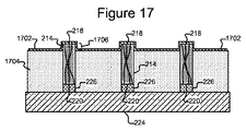
[0094] 図15のステップ1504で、成長基板224上のカーボンナノチューブカラム214の端部分1706を金属化するか、又はその他の方法で、はんだ1602に対して濡れ性の材料(すなわち、はんだ1602が接着する材料)を用いてコーティングすることができる。図17は、カラム214の端部分1706が、金属1702(例えば銅)又ははんだ1602に対して濡れ性の他の材料を用いて金属化される例を示す。図17に示すように、マスキング材料1704は、カラム214周囲の成長基板224上に堆積させることができる。カラム214の端部分1706は、マスキング材料1704の外に延在することができる。カラム214の端部分1706は、端部220から端部218までのカラムの長さ全体よりも短いものとすることができる。例えば、幾つかの実施形態では、端部分1706は、端部220から端部218までのカラム214の長さの5%未満、10%未満、15%未満、20%未満、又は25%未満とすることができる。他の実施形態では、端部分1706は、端部220から端部218までのカラム214の長さの他のパーセンテージとすることができる。 [0094] In step 1504 of FIG. 15, the end portion 1706 of the carbon nanotube column 214 on the growth substrate 224 is metallized or otherwise wettable with respect to the solder 1602 (ie, the solder 1602 is removed). The material to be bonded can be coated. FIG. 17 shows an example where the end portion 1706 of the column 214 is metallized using a metal 1702 (eg, copper) or other material that is wettable to the solder 1602. As shown in FIG. 17, a masking material 1704 can be deposited on the growth substrate 224 around the column 214. The end portion 1706 of the column 214 can extend out of the masking material 1704. The end portion 1706 of the column 214 can be shorter than the entire length of the column from the end 220 to the end 218. For example, in some embodiments, end portion 1706 is less than 5%, less than 10%, less than 15%, less than 20%, or less than 25% of the length of column 214 from end 220 to end 218. can do. In other embodiments, end portion 1706 can be another percentage of the length of column 214 from end 220 to end 218.

[0095] 金属1702は、図17に示すように、マスキング材料1704上、及びカラム214の露出した端部分1706上に堆積させることができる。図を見れば分かるように、マスキング材料1704はカラム214のほとんどをマスクし、露出した端部分1706を除くカラム214上に金属1702が堆積されるのを防ぐ。マスキング材料1704及びマスキング材料1704上の金属1702の部分を除去し、カラム214の端部分1706上の金属1702を残すことができる。幾つかの実施形態では、カラム214をラップするか、又は他の方法で、マスキング材料1704内に包み込みながら平坦化することができる。マスキング材料1704は、成長基板224上に堆積し、その後除去するために好適な、任意の材料とすることができる。マスキング材料1704の非限定的な例は、フォトレジスト及びtrelibondを含む。 [0095] Metal 1702 may be deposited on masking material 1704 and on the exposed end portion 1706 of column 214, as shown in FIG. As can be seen, the masking material 1704 masks most of the column 214 and prevents metal 1702 from being deposited on the column 214 except for the exposed end portions 1706. Masking material 1704 and the portion of metal 1702 on masking material 1704 can be removed, leaving metal 1702 on end portion 1706 of column 214. In some embodiments, the column 214 can be wrapped or otherwise planarized while wrapped within the masking material 1704. The masking material 1704 can be any material suitable for deposition on the growth substrate 224 and subsequent removal. Non-limiting examples of masking material 1704 include photoresist and treribondo.

[0096] 図18は、カラム214の端部を金属1802(例えば銅、ニッケル、金、銀、及び/又はそれらの合金)、又は、はんだに対して濡れ性の他の材料で金属化する別の例を示す。幾つかの実施形態では、金属化の結果、様々な金属(例えば銅、ニッケル、金、銀、又はそれらの合金)の層構造が生じる可能性がある。図18の例で、スパッタリング装置1804は、図に示すように、カラム214に対して角度θで(例えば軸がカラム214の長さと平行に)配置することができる。角度θは、隣接するカラム214が互いにマスクし、カラム214上にスパッタリングされる金属1802が、カラム214の端部分1806上にのみスパッタリングされるように選択することができる。図18に示すように、カラム214bはスパッタリング装置1804を部分的にマスクし、その結果、金属1802は、隣接するカラム214aの端部分1806以外の部分にはスパッタリングされない。角度θは、カラム214の端部分1806が、端部220から端部218までのカラム全体の長さより短いように選択できる。例えば、幾つかの実施形態では、端部分1806は、端部220から端部218までのカラム214の長さの5%未満、10%未満、15%未満、20%未満、又は25%未満とすることができる。他の実施形態では、端部分1806は、端部220から端部218までのカラム214の長さの他のパーセンテージとすることができる。幾つかの実施形態では、スパッタリング装置1804は、成長基板224上でカラム214の端部分1806を金属化するために、成長基板224及びカラムの端部218に対して異なる角度で、及び異なる位置から移動及び位置決めすることができる。 [0096] FIG. 18 shows an alternative to metallizing the end of column 214 with metal 1802 (eg, copper, nickel, gold, silver, and / or alloys thereof) or other materials that are wettable to solder. An example of In some embodiments, metallization can result in layer structures of various metals (eg, copper, nickel, gold, silver, or alloys thereof). In the example of FIG. 18, the sputtering apparatus 1804 can be disposed at an angle θ with respect to the column 214 (for example, the axis is parallel to the length of the column 214) as shown in the figure. The angle θ can be selected such that adjacent columns 214 mask each other and the metal 1802 sputtered on the column 214 is sputtered only on the end portion 1806 of the column 214. As shown in FIG. 18, the column 214b partially masks the sputtering apparatus 1804, so that the metal 1802 is not sputtered on portions other than the end portion 1806 of the adjacent column 214a. The angle θ can be selected such that the end portion 1806 of the column 214 is shorter than the length of the entire column from the end 220 to the end 218. For example, in some embodiments, the end portion 1806 is less than 5%, less than 10%, less than 15%, less than 20%, or less than 25% of the length of the column 214 from the end 220 to the end 218. can do. In other embodiments, end portion 1806 can be other percentages of the length of column 214 from end 220 to end 218. In some embodiments, the sputtering apparatus 1804 may be used to metallize the end portion 1806 of the column 214 on the growth substrate 224 at different angles and from different positions relative to the growth substrate 224 and the column end 218. It can be moved and positioned.

[0097] 金属層(例えば図17の1702又は図18の1802)がカラム214の端部218上にどのように堆積されるかにかかわらず、図19に示すように、カーボンナノチューブカラム214の金属化された端部218を配線基板202の端子212上のはんだ1602に隣接させて位置決めすることによって、図15のステップ1506で、カラム214を配線基板202へと移送することができる。(図19では、金属が図17のように1702として、又は図18のように1802として堆積されたか否かにかかわらず、ラベル1902はカラム218の端部218の金属を表す。したがって、図19における金属1902は、図17のカラム214の端部分1706上の金属1702、又は図18のカラム214の端部分1806上の金属1802を表す。)例えば、金属1902化された端部218をはんだ1602のホール1604内部に位置決めすることができる(図16を参照)。幾つかの実施形態では、カラム214の金属化された1902端部218を端子212に押しつけることができる。 [0097] Regardless of how the metal layer (eg, 1702 in FIG. 17 or 1802 in FIG. 18) is deposited on the end 218 of the column 214, the metal of the carbon nanotube column 214 is shown in FIG. The column 214 can be transferred to the wiring board 202 in step 1506 of FIG. 15 by positioning the segmented end 218 adjacent to the solder 1602 on the terminal 212 of the wiring board 202. (In FIG. 19, label 1902 represents the metal at end 218 of column 218, regardless of whether the metal was deposited as 1702 as in FIG. 17 or as 1802 as in FIG. The metal 1902 in FIG. 17 represents the metal 1702 on the end portion 1706 of the column 214 of FIG. 17 or the metal 1802 on the end portion 1806 of the column 214 of FIG. 18.) For example, the metal 1902 end 218 is soldered 1602 Can be positioned inside the hole 1604 (see FIG. 16). In some embodiments, the metallized 1902 end 218 of the column 214 can be pressed against the terminal 212.

[0098] ステップ1508で、はんだ1602を加熱及びリフローすることができ、これによって、図19に示すように、はんだ1602のフィレット1904を作成することができる。はんだのフィレット1904は、配線基板202の端子212に対して、物理的に固定及び電気的に接続の両方が可能である。上述するように、はんだ1602はカラム214に対して湿潤する(接着する)可能性は低いが、カラム214の端部218の金属1902に対してのみ湿潤する可能性が高い。 [0098] At step 1508, the solder 1602 can be heated and reflowed, thereby creating a fillet 1904 of the solder 1602, as shown in FIG. The solder fillet 1904 can be both physically fixed and electrically connected to the terminal 212 of the wiring board 202. As described above, solder 1602 is unlikely to wet (adhere) to column 214, but is likely to wet only to metal 1902 at end 218 of column 214.

[0099] 図15のステップ1510で、カラム214は、その後除去することができる成長基板224から切り離すことができる。カラム214は、カラム214から成長基板224を物理的に引き抜く、溶媒を使用するなどを含む、任意の好適な方法で、成長基板224から切り離すことができる。 [0099] In step 1510 of FIG. 15, the column 214 can be detached from the growth substrate 224, which can then be removed. The column 214 can be separated from the growth substrate 224 by any suitable method, including physically pulling the growth substrate 224 from the column 214, using a solvent, and the like.

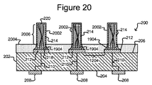
[00100] 図20は、本発明の幾つかの実施形態による、カラム214上に金属コーティング2002を提供可能なオプションのプロセスを示す。図20に示すように、カラム214の部分2006がマスキング材料2004の外に延在するように、カラム214間の配線基板202上にマスキング材料2004を堆積させることができる。図を見れば分かるように、マスキング材料2004は、金属コーティング2002(例えば、金、銀、銅、又は同様の金属)の堆積をマスクする。したがって、マスキング材料2004の外に延在するカラム214の部分2006は、その上に金属コーティング2002を堆積させることが望ましい各カラム214の部分に対応することができる。配線基板202上のマスキング材料2004の高さは、マスキング材料2004の外に延在するカラム214の部分2006の長さが所望なようにすることができる。幾つかの実施形態では、マスキング材料2004は端子212まで延在でき、結果として金属コーティング2002が端子212まで延在する。幾つかの実施形態では、マスキング材料2004は、はんだフィレット1904まで延在でき、結果として金属コーティング2002がはんだフィレット1904まで延在する。しかし、マスキング材料2004は、配線基板202上への堆積及びその後の配線基板202からの除去に好適な任意の材料とすることができる。マスキング材料2004の非限定的な例は、フォトレジスト及びtrelibondを含む。次に、金属コーティング2002は、図20に示すように、カラム上に堆積させることができる。マスキング材料2004は、金属コーティング2002がカラム2004の露出部分2006以外のいずれかに堆積するのを防ぐことができる。金属コーティング2002は、電気めっき、無電解めっき、スパッタリングなどを含む任意の好適な堆積方法を使用して堆積させることができる。マスキング材料2004は、次に、マスキング材料2004上に蓄積されたいずれかの金属コーティング2002と共に除去することができる。 [00100] FIG. 20 illustrates an optional process that can provide a metal coating 2002 on the column 214 according to some embodiments of the invention. As shown in FIG. 20, a masking material 2004 can be deposited on the wiring substrate 202 between the columns 214 such that a portion 2006 of the column 214 extends out of the masking material 2004. As can be seen, the masking material 2004 masks the deposition of a metal coating 2002 (eg, gold, silver, copper, or similar metal). Accordingly, the portion 2006 of column 214 that extends out of masking material 2004 may correspond to the portion of each column 214 on which it is desired to deposit a metal coating 2002. The height of the masking material 2004 on the wiring substrate 202 can be such that the length of the portion 2006 of the column 214 that extends out of the masking material 2004 is desired. In some embodiments, the masking material 2004 can extend to the terminal 212, resulting in the metal coating 2002 extending to the terminal 212. In some embodiments, the masking material 2004 can extend to the solder fillet 1904, resulting in the metal coating 2002 extending to the solder fillet 1904. However, the masking material 2004 can be any material suitable for deposition on the wiring substrate 202 and subsequent removal from the wiring substrate 202. Non-limiting examples of masking material 2004 include photoresist and trelibond. Next, a metal coating 2002 can be deposited on the column, as shown in FIG. The masking material 2004 can prevent the metal coating 2002 from depositing anywhere on the column 2004 other than the exposed portion 2006. Metal coating 2002 can be deposited using any suitable deposition method, including electroplating, electroless plating, sputtering, and the like. The masking material 2004 can then be removed along with any metal coating 2002 accumulated on the masking material 2004.

[00101] 再度図1のプロセス100を参照すると、カラム214の端部にコンタクトチップを提供できる。図21A、図21B、及び図22は、カラム214の端部220にコンタクトチップ2102を提供する例を示し、図24は、カラム214の端部220にコンタクトチップ2402を提供する別の例を示す。図25A及び図25Bは、コンタクトチップを提供する別の例を示す。 [00101] Referring again to the process 100 of FIG. 1, a contact tip can be provided at the end of the column 214. 21A, 21B, and 22 show an example of providing a contact tip 2102 at the end 220 of the column 214, and FIG. 24 shows another example of providing a contact tip 2402 at the end 220 of the column 214. . 25A and 25B show another example of providing a contact chip.

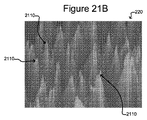
[00102] 図21Aに示すように、マスキング材料2106(例えば、マスキング材料1704又は2004など)は配線基板202上に堆積させることができ、カラム214の端部220はマスキング材料2106の外へ延在できるため露出される。次に、カラム214の露出した端部220は、カラム214の端部220で鋭利な構造を作成するために粗面化することができる。例えば、カラムの端部220に、カラム214の端部に鋭利な構造を作成するプラズマ処理を施すことができる。図21Bは、このような鋭利な構造2110の例を示すカーボンナノチューブのカラム214の端部220の写真を示す。マスキング材料2106は、マスキング材料2106内に包み込まれたカラム214の部分をこのような処理から保護することができる。 [00102] As shown in FIG. 21A, a masking material 2106 (eg, masking material 1704 or 2004, etc.) can be deposited on the wiring substrate 202, and the end 220 of the column 214 extends out of the masking material 2106. It is exposed as possible. The exposed end 220 of the column 214 can then be roughened to create a sharp structure at the end 220 of the column 214. For example, the column end 220 can be subjected to a plasma treatment that creates a sharp structure at the end of the column 214. FIG. 21B shows a photograph of the end 220 of the carbon nanotube column 214 showing an example of such a sharp structure 2110. Masking material 2106 can protect the portion of column 214 encapsulated within masking material 2106 from such processing.

[00103] カラム214の粗面化された端部220は、次に、粗面化された端部220上に導電性金属2104(例えば、金、銀、銅など)を堆積させることによって、金属化することができる。図21Aに示すように、マスキング材料2106は、金属2104が、配線基板202上、及び露出された端部220を除くカラム214上のいずれかに堆積するのを防ぐことができる。あるいは、図22に示すように、マスキング材料2206(部分的に除去されたマスキング材料2106、又はマスキング材料2106を除去した後に配線基板202上に堆積された新しいマスキング材料とすることができる)は、カラム214をさらに露出させることができるため、結果として金属2104は、カラムの端部220上のみならず、マスキング材料2206(マスキング材料2106などとすることができる)を通して露出されるカラムの部分上にも堆積する。しかし、金属2104で金属化された後、マスキング材料2106又は2206を除去することができる。各カラムの金属化され粗面化された端部220は、コンタクトチップ2102とすることができ、これは図2A及び図2Bのコンタクトチップ228の例とすることができる。 [00103] The roughened end 220 of the column 214 is then metallized by depositing a conductive metal 2104 (eg, gold, silver, copper, etc.) on the roughened end 220. Can be As shown in FIG. 21A, the masking material 2106 can prevent the metal 2104 from depositing either on the wiring substrate 202 and on the column 214 except for the exposed ends 220. Alternatively, as shown in FIG. 22, the masking material 2206 (which can be a partially removed masking material 2106 or a new masking material deposited on the wiring substrate 202 after removing the masking material 2106) As column 214 can be further exposed, the resulting metal 2104 is not only on the end 220 of the column, but also on the portion of the column that is exposed through masking material 2206 (which can be masking material 2106, etc.). Also deposits. However, after metallization with metal 2104, masking material 2106 or 2206 can be removed. The metallized and roughened end 220 of each column can be a contact tip 2102, which can be an example of the contact tip 228 of FIGS. 2A and 2B.

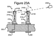
[00104] 図23Aは、スパッタリング装置2304が、図18に示すプロセスと同様であってよいプロセスで、カラム214の端部分2306上に金属2104をスパッタリングする、カラム214の端部220を金属2104で金属化する別の例を示す。図23Aの例で、スパッタリング装置2304は、カラム214に対して(例えばカラム214の長さと平行な軸に対して)角度θで配置することができる。角度θは、隣接するカラム214が互いにマスクし、カラム214上にスパッタリングされる金属2104が、カラム214の端部分2306上にのみスパッタリングされるように選択することができる。図23Aに示すように、カラム214bはスパッタリング装置2304を部分的にマスクし、その結果、金属2104は、端部分2306以外の隣接するカラム214aの部分にはスパッタリングされない。角度θは、カラム214の端部分2306が、端部218から端部220までのカラム全体の長さより短いように選択できる。例えば、幾つかの実施形態では、端部分2306は、端部218から端部220までのカラム214の長さの5%未満、10%未満、15%未満、20%未満、又は25%未満とすることができる。他の実施形態では、端部分2306は、端部218から端部220までのカラム214の長さの他のパーセンテージとすることができる。幾つかの実施形態では、スパッタリング装置2304は、配線基板202上でカラム214の端部分2306を金属化するために、配線基板202及びカラムの端部220に対して異なる角度で、及び異なる位置から移動及び位置決めすることができる。図23Bは、金属2104がカラム214の端部分2306上にのみ堆積されたカーボンナノチューブカラム214の写真を示す。図23Bで、金属2104は、金属2104が堆積されていないカラム214の部分よりも色が薄い。 [00104] FIG. 23A is a process in which the sputtering apparatus 2304 may be similar to the process shown in FIG. 18 to sputter the metal 2104 onto the end portion 2306 of the column 214 and the end 220 of the column 214 with the metal 2104. Another example of metallization is shown. In the example of FIG. 23A, the sputtering apparatus 2304 can be positioned at an angle θ relative to the column 214 (eg, relative to an axis parallel to the length of the column 214). The angle θ can be selected such that adjacent columns 214 mask each other and the metal 2104 sputtered onto the column 214 is sputtered only onto the end portion 2306 of the column 214. As shown in FIG. 23A, column 214b partially masks sputtering apparatus 2304, so that metal 2104 is not sputtered onto portions of adjacent column 214a other than end portion 2306. The angle θ can be selected such that the end portion 2306 of the column 214 is shorter than the entire length of the column from the end 218 to the end 220. For example, in some embodiments, end portion 2306 is less than 5%, less than 10%, less than 15%, less than 20%, or less than 25% of the length of column 214 from end 218 to end 220. can do. In other embodiments, end portion 2306 can be other percentages of the length of column 214 from end 218 to end 220. In some embodiments, the sputtering apparatus 2304 is configured to metallize the end portion 2306 of the column 214 on the wiring substrate 202 at different angles and from different positions with respect to the wiring substrate 202 and the column end 220. It can be moved and positioned. FIG. 23B shows a photograph of the carbon nanotube column 214 with metal 2104 deposited only on the end portion 2306 of the column 214. In FIG. 23B, metal 2104 is lighter in color than the portion of column 214 where metal 2104 is not deposited.

[00105] 図24は、カラム214の端部220にコンタクトチップを提供する別の例を示し、図21A、図21B、図22、図23A、及び図23Bに示すプロセスの代替方法を表す。図に示すように、コンタクトチップ構造2402は基板2406上に提供できる。例えばコンタクトチップ構造2402は、配線基板202上のカラム214の端部220のパターンに対応するパターンで、基板2406上で製造できる。コンタクトチップ構造2402は、カップリング2404によってカラム214の端部220に接合された後に、基板2406から切り離すことができる。カップリング2404は、チップ構造2402をカラム214の端部220に接合するための任意の好適な材料とすることができる。例えばカップリング2404は、はんだ又は同様の接合材料を含むことができる。別の例として、カップリング2404は、図14のフィレット1402のような焼結されたナノペースト(例えばナノペースト1202など)を含むことができる。コンタクトチップ2402は、図2A及び図2Bのコンタクトチップ228の代替例とすることができる。 [00105] FIG. 24 shows another example of providing a contact tip at the end 220 of the column 214 and represents an alternative method of the process shown in FIGS. 21A, 21B, 22, 23A, and 23B. As shown, a contact chip structure 2402 can be provided on a substrate 2406. For example, the contact chip structure 2402 can be manufactured on the substrate 2406 in a pattern corresponding to the pattern of the end portion 220 of the column 214 on the wiring substrate 202. Contact tip structure 2402 can be detached from substrate 2406 after being joined to end 220 of column 214 by coupling 2404. The coupling 2404 can be any suitable material for joining the tip structure 2402 to the end 220 of the column 214. For example, the coupling 2404 can include solder or similar bonding material. As another example, coupling 2404 can include a sintered nanopaste (such as nanopaste 1202) such as fillet 1402 of FIG. Contact chip 2402 may be an alternative to contact chip 228 of FIGS. 2A and 2B.

[00106] 図25A及び図25は、カラム214の端部220にコンタクトチップ228を提供する別の例を示し、図21A、図21B、図22、図23A、図23B、及び図24に示すプロセスの代替方法を表す。図25Aに示すように、導電性材料の粒子を含むナノペースト2554をカラム214の端部220上に堆積させることができる。ナノペースト2554は、溶媒中に導電性材料(例えば、金、銀、銅、又は同様の金属)の粒子を含むことができる。粒子はナノ粒子とすることができる。幾つかの実施形態では、ナノペースト2554は、ルテニウム又はロジウムなどの硬質材料とすることができる微粒子及び/又は鋭利な粒子を含むこともできる。
[00106] FIGS. 25A and 25 B show another example of providing a contact tip 228 on the end 220 of the column 214, FIG. 21A, FIG. 21B, FIG. 22, FIG. 23A, FIG. 23B, and FIG. 24 Represents an alternative process. As shown in FIG. 25A, nanopaste 2554 comprising particles of conductive material can be deposited on the end 220 of the column 214. Nanopaste 2554 can include particles of a conductive material (eg, gold, silver, copper, or similar metal) in a solvent. The particles can be nanoparticles. In some embodiments, the nanopaste 2554 can also include fine particles and / or sharp particles that can be a hard material such as ruthenium or rhodium.

[00107] ナノペースト2554は、任意の好適な方法で、カラム214の端部220上に堆積させることができる。例えば、図25Aに示すように、幾つかの実施形態では、ナノペースト2554は、プリントヘッド2552(例えばインクジェットプリントヘッド)を通してカラム214の端部220上にプリントすることができる。あるいは、ナノペースト2554は、スクリーンプリント、マスクなどの他の方法を使用して、カラム214の端部220上に堆積させることができる。次に、ナノペースト2554は硬化させることができる。例えばナノペースト2554は、温度制御デバイス2556(例えばヒータ)を使用して、ナノペースト2554が硬化するのに十分な温度まで、及び時間だけ加熱することができる。幾つかの実施形態では、ナノペーストを焼結させることができる。 [00107] The nanopaste 2554 can be deposited on the end 220 of the column 214 in any suitable manner. For example, as shown in FIG. 25A, in some embodiments, nanopaste 2554 can be printed on end 220 of column 214 through printhead 2552 (eg, an inkjet printhead). Alternatively, the nanopaste 2554 can be deposited on the end 220 of the column 214 using other methods such as screen printing, masking and the like. The nanopaste 2554 can then be cured. For example, the nanopaste 2554 can be heated using a temperature control device 2556 (eg, a heater) to a temperature sufficient for the nanopaste 2554 to cure and for a period of time. In some embodiments, the nanopaste can be sintered.

[00108] 図25Bに示すように、硬化したナノペーストはカラムの端部220にコンタクトチップ2558を形成することができる。ナノ粒子は、カラムの端部220に導電性コーティングを形成することができる。コンタクトチップ2558は、図2A及び図2Bのコンタクトチップ228の別の例とすることができる。 [00108] As shown in FIG. 25B, the cured nanopaste can form a contact tip 2558 at the end 220 of the column. The nanoparticles can form a conductive coating at the end 220 of the column. Contact chip 2558 may be another example of contact chip 228 of FIGS. 2A and 2B.

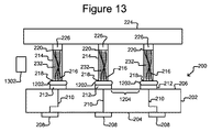
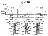
[00109] 再度図1のプロセス100を参照すると、ステップ110で、電子装置を形成するために配線基板202を1つ又は複数の他の要素に結合させることができる。図26は、プローブカードアセンブリ2500を形成するために配線基板202が他の電子要素に結合される例を示し、図27は、被試験デバイス(DUT)2618に接触し、これをテストするためにプローブカードアセンブリ2500が使用できるテストシステム2600の例を示す。 [00109] Referring again to the process 100 of FIG. 1, at step 110, the wiring board 202 may be coupled to one or more other elements to form an electronic device. FIG. 26 illustrates an example in which the wiring board 202 is coupled to other electronic elements to form a probe card assembly 2500, and FIG. 27 illustrates contact with a device under test (DUT) 2618 for testing it. 6 illustrates an example test system 2600 in which the probe card assembly 2500 can be used.

[00110] プローブカードアセンブリ2500は、図1のステップ110の例として、スティフナ構造2502と、配線基板202を物理的及び電気的に結合することができる配線板2508とを含むことができる。図26に示すように、結合メカニズム2504は、プローブカードアセンブリ2500に剛性を与える剛性構造(例えば、金属又は他の剛性材料を含む)とすることができるスティフナ構造2502に、配線基板202を物理的に結合することができる。スティフナ2502は、プローブカードアセンブリ2500を図27のテストシステム2600内のハウジング2620の装着面2610に結合するための手段(図示せず)を含むこともできる。結合メカニズム2504は、配線基板202をスティフナ2502に物理的に結合するために好適な任意のメカニズムを含むことができる。例えば結合メカニズム2504は、ねじ、ボルト、クランプなどを含むことができる。幾つかの実施形態では、結合メカニズム2504は、配線基板202をスティフナ2502に可動式に結合する差動ねじアセンブリ(図示せず)などの可動メカニズムを含むことができる。 [00110] The probe card assembly 2500 can include a stiffener structure 2502 and a wiring board 2508 that can physically and electrically couple the wiring board 202 as an example of step 110 of FIG. As shown in FIG. 26, the coupling mechanism 2504 physically attaches the wiring board 202 to the stiffener structure 2502, which can be a rigid structure (eg, including metal or other rigid material) that provides rigidity to the probe card assembly 2500. Can be combined. Stiffener 2502 may also include means (not shown) for coupling probe card assembly 2500 to mounting surface 2610 of housing 2620 in test system 2600 of FIG. The coupling mechanism 2504 can include any mechanism suitable for physically coupling the wiring board 202 to the stiffener 2502. For example, the coupling mechanism 2504 can include screws, bolts, clamps, and the like. In some embodiments, the coupling mechanism 2504 can include a movable mechanism such as a differential screw assembly (not shown) that movably couples the wiring board 202 to the stiffener 2502.

[00111] さらに図26を参照すると、図27のテストコントローラ2602などのテストコントローラとの間の別個の通信チャネルに対する電気インターフェイス2506(例えばゼロ挿入力(ZIF)電気コネクタ、ポゴピンパッド、又は他のこのような電気コネクタ)を配線板2508上に配置することができる。電気接続2510(例えば、配線板2508の上及び/又は内部の導電性ビア及び/又はトレース)は、配線板2508を通して電気インターフェイス2506からの電気接続を提供することができる。配線板2508は、プリント回路板などの半剛性基板又はセラミック配線板などの剛性基板とすることができる。 [00111] Still referring to FIG. 26, an electrical interface 2506 (eg, a zero insertion force (ZIF) electrical connector, a pogo pin pad, or other such) to a separate communication channel with a test controller such as test controller 2602 of FIG. Such an electrical connector) can be disposed on the wiring board 2508. Electrical connection 2510 (eg, conductive vias and / or traces on and / or within wiring board 2508) can provide an electrical connection from electrical interface 2506 through wiring board 2508. The wiring board 2508 can be a semi-rigid board such as a printed circuit board or a rigid board such as a ceramic wiring board.

[00112] 図26に示すように、電気接続2512は、配線板2508を通して電気接続2510を配線基板202の端子208に電気的に接続することができる。電気接続2512は、配線板2508を端子208に電気的に接続する任意の好適な接続とすることができる。例えば、電気接続2512は、フレキシブルワイヤ又はインタポーザ(図示せず)などの可撓性電気接続とすることができる。別の例として、電気接続2512は、はんだ又は他の同様の電気的導電性接合材料とすることができる。 As shown in FIG. 26, the electrical connection 2512 can electrically connect the electrical connection 2510 to the terminal 208 of the wiring board 202 through the wiring board 2508. The electrical connection 2512 can be any suitable connection that electrically connects the wiring board 2508 to the terminal 208. For example, electrical connection 2512 can be a flexible electrical connection, such as a flexible wire or an interposer (not shown). As another example, electrical connection 2512 can be solder or other similar electrically conductive bonding material.

[00113] 配線基板202の端子212に結合されたカーボンナノチューブカラム214はばねプローブ240とすることができ、コンタクトチップ228は、図27のテストシステム2600でテストされるDUT2618に対応するパターンで配置できる。頭字語「DUT」は、(単体化されるか又はウェーハ形式の、又はパッケージ化されるか又はパッケージ化されない)半導体ダイを含むが限定的でない任意の電子デバイスとすることができる「被試験デバイス」を意味することができる。図26に示すように、プローブカードアセンブリ2500は、端子を通して各プローブ240を、配線基板202を通して電気接続210を、端子208、電気接続2512、及び配線板2508を通して電気接続2510を電気インターフェイス2506へ電気的に接続する。 [00113] The carbon nanotube column 214 coupled to the terminal 212 of the wiring board 202 can be a spring probe 240, and the contact tips 228 can be arranged in a pattern corresponding to the DUT 2618 tested in the test system 2600 of FIG. . The acronym “DUT” refers to “device under test,” which can be any electronic device including but not limited to a semiconductor die (single or in wafer form, or packaged or not packaged). Can mean. As shown in FIG. 26, probe card assembly 2500 electrically connects each probe 240 through terminals, electrical connection 210 through wiring board 202, and electrical connection 2510 through terminal 208, electrical connection 2512, and wiring board 2508 to electrical interface 2506. Connect.

[00114] 上述のように、図25のプローブカードアセンブリ2500を使用して、内部でプローブカードアセンブリ2500を使用することが可能なテストシステム2600の例を示す、図27のDUT2618などの電子デバイスをテストすることができる。図27に示すように、テストシステム2600は、DUT2618に入力信号を提供でき、入力信号に応答してDUT2618によって生成された応答信号を受信できるテストコントローラ2602を含むことができる。「テスト信号」という用語は、テストコントローラ2602によって生成された入力信号及びDUT2618によって生成された応答信号のいずれか又は両方を総称的に言い表すことができる。プローブカードアセンブリ2500は、テストシステム2600のハウジング2620(例えばプローバ)の装着面2610に結合できる。プローブカードアセンブリ2500のプローブ240は、DUT2618の端子2616との圧力ベースの電気接続を行うことができ、テストコントローラ2602と、通信接続2604(例えば同軸ケーブル、無線リンク、光ファイバリンクなど)を介したDUT2618、テストヘッド2606内の電子部品(図示せず)、テストヘッド2606とプローブカードアセンブリ2602の電気インターフェイス2506との間のコネクタ2608、並びにプローブカードアセンブリ2600の間でテスト信号を渡すことができる。図に示すように、プローブカードアセンブリ2600は、その上にDUT2618が配置される可動チャック2624を含むことができるハウジング2620の装着面2610に結合できる。 [00114] As described above, the probe card assembly 2500 of FIG. 25 is used to illustrate an electronic device such as the DUT 2618 of FIG. 27 that illustrates an example of a test system 2600 that can use the probe card assembly 2500 therein. Can be tested. As shown in FIG. 27, the test system 2600 can include a test controller 2602 that can provide an input signal to the DUT 2618 and receive a response signal generated by the DUT 2618 in response to the input signal. The term “test signal” can generically describe either or both of an input signal generated by the test controller 2602 and a response signal generated by the DUT 2618. Probe card assembly 2500 can be coupled to mounting surface 2610 of housing 2620 (eg, a prober) of test system 2600. Probe 240 of probe card assembly 2500 can make a pressure-based electrical connection with terminal 2616 of DUT 2618 via a test controller 2602 and a communication connection 2604 (eg, coaxial cable, wireless link, fiber optic link, etc.). Test signals can be passed between the DUT 2618, electronic components (not shown) within the test head 2606, the connector 2608 between the test head 2606 and the electrical interface 2506 of the probe card assembly 2602, and the probe card assembly 2600. As shown, the probe card assembly 2600 can be coupled to a mounting surface 2610 of a housing 2620 that can include a movable chuck 2624 on which a DUT 2618 is disposed.

[00115] DUT2518は以下のようにテストできる。プローブカードアセンブリ2500はハウジング2620の装着面2610に結合でき、DUT2618の端子2616をプローブカードアセンブリ2500のプローブ240と接触させることができる。これは、DUT2618の端子2616がプローブカードアセンブリ2500のプローブ240に対して押しつけられるように、チャック2624を移動させることによって達成できる。あるいは、端子2616とプローブ240との間の接触を有効にするために、プローブカードアセンブリ2500が移動できるか、又はチャック2624とプローブカードアセンブリ2500の両方が移動できる。 [00115] The DUT 2518 can be tested as follows. Probe card assembly 2500 can be coupled to mounting surface 2610 of housing 2620 and terminal 2616 of DUT 2618 can be in contact with probe 240 of probe card assembly 2500. This can be accomplished by moving the chuck 2624 such that the terminal 2616 of the DUT 2618 is pressed against the probe 240 of the probe card assembly 2500. Alternatively, the probe card assembly 2500 can be moved, or both the chuck 2624 and the probe card assembly 2500 can be moved to enable contact between the terminal 2616 and the probe 240.

[00116] プローブ240と端子2616が接触している間に、テストコントローラ2602とDUTとの間にプローブカードアセンブリ2500を通してテスト信号(上述のように、テストコントローラ2602によって生成される入力信号と、入力信号に応答してDUT2618によって生成される応答信号とを含むことができる)を提供することにより、DUT2618をテストすることができる。テストコントローラ2602は、応答信号を分析して、DUT2618がテストに合格であるか否かを判定することができる。例えば、テストコントローラ2602は、この応答信号と予測された応答信号とを比較することができる。応答信号が予測された応答信号と一致した場合、テストコントローラ2602は、DUT2618がテストに合格したものと判定することができる。一致しない場合、テストコントローラ2602は、DUT2618がテストに不合格であったものと判定することができる。別の例として、テストコントローラ2602は、応答信号が許容範囲内にあるか否かを判定でき、範囲内にある場合、DUT2618がテストに合格したものと判定することができる。 [00116] While the probe 240 and terminal 2616 are in contact, the test signal (as described above, the input signal generated by the test controller 2602 and the input through the probe card assembly 2500 between the test controller 2602 and the DUT DUT 2618 can be tested by providing a response signal generated by DUT 2618 in response to the signal. Test controller 2602 can analyze the response signal to determine whether DUT 2618 passes the test. For example, the test controller 2602 can compare this response signal with the predicted response signal. If the response signal matches the predicted response signal, the test controller 2602 can determine that the DUT 2618 has passed the test. If they do not match, the test controller 2602 can determine that the DUT 2618 has failed the test. As another example, the test controller 2602 can determine whether the response signal is within an acceptable range, and if so, can determine that the DUT 2618 has passed the test.

[00117] 図26のプローブカードアセンブリ2500は単なる例示としてのものであり、図2A及び図2Bに関して上述したように、本明細書で説明されるカーボンナノチューブカラム214は他の電子デバイス内でも使用できる。例えば、カーボンナノチューブカラム214は、半導体ダイ又は他の電子プローブデバイスをテストするためのテストソケット内のコンタクトプローブ(図示せず)として使用できる。図27のテストシステム2600も単なる例示としてのものであり、図26のプローブカードアセンブリ2500は他のテストシステムで使用できる。さらに別の例では、カーボンナノチューブカラム214を使用して、複数のダイ及び配線基板を備えるシステムをアセンブルすることができる(例えば、カーボンナノチューブカラム214はダイを相互接続すること、及びダイを配線基板に接続することができる)。 [00117] The probe card assembly 2500 of FIG. 26 is merely exemplary, and as described above with respect to FIGS. 2A and 2B, the carbon nanotube column 214 described herein can be used in other electronic devices. . For example, the carbon nanotube column 214 can be used as a contact probe (not shown) in a test socket for testing a semiconductor die or other electronic probe device. The test system 2600 of FIG. 27 is also exemplary only, and the probe card assembly 2500 of FIG. 26 can be used with other test systems. In yet another example, the carbon nanotube column 214 can be used to assemble a system comprising multiple dies and a wiring substrate (eg, the carbon nanotube column 214 interconnects the dies and the die on the wiring substrate). Can be connected to).

[00118] カーボンナノチューブを備えるプローブ240は、図26及び図27に示すようなテストシステム又はプローブカードアセンブリでの使用に限定されるものではない。 [00118] The probe 240 comprising carbon nanotubes is not limited to use in a test system or probe card assembly as shown in FIGS.

[00119] 図28は、カーボンナノチューブを備えるプローブ240が、プローブ240がカップリング230によってテスト基板2810の端子2812に結合されるテストソケット2800内で使用できる非限定的な例を示す。図28は、クリップ、支持フレーム2806、及び、カップリング230によってプローブ240が結合可能な端子2812を備えたテスト基板2810を備えることができる例示的テストソケット2800を示す。このプローブ240は、上述のように、プローブ240が基板202の端子212に結合される方法と同じか又は同様の方法で、カップリング230によってテスト基板2810の端子2812に結合できる。 [00119] FIG. 28 illustrates a non-limiting example where a probe 240 comprising carbon nanotubes can be used in a test socket 2800 where the probe 240 is coupled to a terminal 2812 of a test substrate 2810 by a coupling 230. FIG. 28 illustrates an exemplary test socket 2800 that can include a clip, a support frame 2806, and a test board 2810 with a terminal 2812 to which the probe 240 can be coupled by a coupling 230. The probe 240 can be coupled to the terminal 2812 of the test substrate 2810 by the coupling 230 in the same or similar manner as the probe 240 is coupled to the terminal 212 of the substrate 202 as described above.

[00120] 図28に示すように、テストソケット2800を使用して、単一化された半導体ダイ2816(パッケージ化されるか又はパッケージ化されない)などの電子デバイスをテストすることができる。図28に示すように、それによってダイ2806を支持フレーム2806上に配置することが可能なクリップ2802を支持フレーム2806から除去することができる。支持フレーム2806は、ダイ2816の端子2804(例えばバンプ)がプローブ240と接触する位置に各ダイ2816を誘導する傾斜壁2808を有することができる。次に、クリップ2802は、支持フレーム2806上にクリップされ、ダイ2816の端子2804とプローブ240との間の電気接続を確立するために十分な力で、ダイ2816の端子2804をプローブ240に押しつけることができる。配線基板2010は、端子2812から、したがってプローブ240から、ダイ2816のテストを制御するためのテストコントローラ(図示せず)への、電気接続(図示せず)を含むことができる。ダイ2816がテストされると、クリップ2802を支持フレーム2806から除去することができ、ダイ2816をソケット2800から除去することができる。ソケット2800は、テストソケットであるというよりむしろ、又はテストソケットであることに加えて、テストソケットであるダイ2816及び基板2810がその一部である電子システムとすることができる。このようなケースでは、代替的に又は追加的に、テスト基板2810は電子システムの一部である配線基板とすることができる。 [00120] As shown in FIG. 28, a test socket 2800 may be used to test an electronic device, such as a singulated semiconductor die 2816 (packaged or not packaged). As shown in FIG. 28, the clip 2802 that allows the die 2806 to be placed on the support frame 2806 can be removed from the support frame 2806. The support frame 2806 can have inclined walls 2808 that guide each die 2816 to a location where the terminals 2804 (eg, bumps) of the die 2816 contact the probe 240. The clip 2802 is then clipped onto the support frame 2806, pressing the terminal 2804 of the die 2816 against the probe 240 with sufficient force to establish an electrical connection between the terminal 2804 of the die 2816 and the probe 240. Can do. The wiring board 2010 can include electrical connections (not shown) from the terminals 2812 and thus from the probe 240 to a test controller (not shown) for controlling the testing of the die 2816. When die 2816 is tested, clip 2802 can be removed from support frame 2806 and die 2816 can be removed from socket 2800. Rather than being a test socket or in addition to being a test socket, the socket 2800 can be an electronic system of which the test socket die 2816 and substrate 2810 are a part. In such a case, alternatively or additionally, the test board 2810 can be a wiring board that is part of the electronic system.

[00121] テストソケット2800は単なる例示としてのものであり、変形が可能である。例えば、図28には2つのダイ2816が示されているが、テストソケット2800は2つより多くの又はより少ないダイ2816を保持するように構成することができる。別の例として、クリップ2802及び/又は支持フレーム2806は、図28に示す形状と異なる形状であり得る。 [00121] The test socket 2800 is merely exemplary and can be modified. For example, although two dies 2816 are shown in FIG. 28, the test socket 2800 can be configured to hold more or fewer dies 2816. As another example, the clip 2802 and / or the support frame 2806 can have a different shape from that shown in FIG.

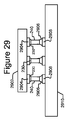
[00122] 図29は、カーボンナノチューブを備えるプローブ240を使用して2つの電子デバイス2902及び2910を電気的に接続するのに使用できる非限定的な例を示す。図に示すように、プローブ240はカップリング230によって電子デバイス2902に結合できる。プローブ240は、上述のようにプローブ240が基板202の端子212に結合される方法と同じか又は同様の方法で、カップリング230によって電子デバイス2902の端子2904に結合できる。図29にも示すように、プローブ240は、接合材料2906(例えばはんだ)によって電子デバイス2910の端子2908に接合できる。したがって電子デバイス2902は、プローブ240によって電子デバイス2910に電気的に接続できる。電子デバイス2902及び2910は、互いに電気的に接続可能な任意の電子デバイスとすることができる。例えば、電子デバイス2902及び2910は、どちらも半導体ダイ(パッケージ化されるか又はパッケージ化されない)とすることができる。別の例として、電子デバイス2902又は2910のうちの一方がこのような半導体ダイであり、電子デバイス2902又は2910のうちの他方はプリント回路板とすることができる。図29に示す構成は単なる例示としてのものであり、変形が可能である。例えば、電子デバイス2902及び2910のサイズ、形状、及び位置は、図29に示すものと異なるものとすることができる。別の例として、2つの電子デバイス2902及び2910よりも多くの電子デバイスを使用することもできる。さらに別の例として、電子デバイス2902及び2910のうちの1つ又は両方が、3つより多いか又は少ない端末2904及び2908を有することができ、3つより多いか又は少ないプローブ240を使用することもできる。 [00122] FIG. 29 illustrates a non-limiting example that can be used to electrically connect two electronic devices 2902 and 2910 using a probe 240 comprising carbon nanotubes. As shown, probe 240 can be coupled to electronic device 2902 by coupling 230. Probe 240 can be coupled to terminal 2904 of electronic device 2902 by coupling 230 in the same or similar manner as probe 240 is coupled to terminal 212 of substrate 202 as described above. As also shown in FIG. 29, the probe 240 can be bonded to the terminal 2908 of the electronic device 2910 by a bonding material 2906 (eg, solder). Accordingly, the electronic device 2902 can be electrically connected to the electronic device 2910 by the probe 240. Electronic devices 2902 and 2910 may be any electronic devices that can be electrically connected to each other. For example, electronic devices 2902 and 2910 can both be semiconductor dies (packaged or unpackaged). As another example, one of electronic devices 2902 or 2910 can be such a semiconductor die and the other of electronic devices 2902 or 2910 can be a printed circuit board. The configuration shown in FIG. 29 is merely an example and can be modified. For example, the size, shape, and position of electronic devices 2902 and 2910 can be different from those shown in FIG. As another example, more electronic devices than the two electronic devices 2902 and 2910 can be used. As yet another example, one or both of electronic devices 2902 and 2910 can have more or less than three terminals 2904 and 2908, using more or less than three probes 240. You can also.

[00123] 本明細書では本発明の特定の実施形態及び用途について説明してきたが、これらの実施形態及び用途は単なる例示としてのものであり、多くの変形が可能である。 [00123] While specific embodiments and applications of the invention have been described herein, these embodiments and applications are merely exemplary and many variations are possible.

Claims (7)

プローブカードアセンブリであって、
テストされる電子デバイスのテストを制御するためのテスターへの電気インターフェイスを備える配線基板と、
テストされる前記電子デバイスの端子に対応するパターンで配置された複数のプローブを備えるプローブ基板であって、それぞれの前記プローブが、カーボンナノチューブのバンドルを含むカーボンナノチューブカラムを備えるプローブ基板と、
前記カーボンナノチューブカラムのうちの1つを前記プローブ基板の複数の端子のうちの1つに接合する接着材料接合部であって、それぞれの前記接着材料接合部が、前記カーボンナノチューブカラムのうちの前記1つのカーボンナノチューブカラムと、前記複数の端子のうちの前記1つの端子とに溶着された焼結ナノ粒子の塊を含む、接着材料接合部と、
を備え、
前記プローブ基板が前記配線基板に機械的に結合され、前記プローブが、前記プローブ基板及び前記配線基板を通して前記電気インターフェイスに電気的に接続されるプローブカードアセンブリ。
A probe card assembly,
A wiring board with an electrical interface to a tester for controlling the testing of the electronic device to be tested;
A probe substrate comprising a plurality of probes arranged in a pattern corresponding to the terminal of the electronic device to be tested, each of said probe, and a probe substrate including a carbon nanotube column containing bundles of mosquitoes over carbon nanotubes,
An adhesive material joint for joining one of the carbon nanotube columns to one of a plurality of terminals of the probe substrate, wherein each of the adhesive material joints is the one of the carbon nanotube columns. An adhesive material joint comprising a carbon nanotube column and a mass of sintered nanoparticles welded to the one of the plurality of terminals;
With
A probe card assembly, wherein the probe board is mechanically coupled to the wiring board, and the probe is electrically connected to the electrical interface through the probe board and the wiring board.
それぞれの前記カーボンナノチューブカラムが、前記カーボンナノチューブの長さに沿った複数の交互の剛性領域及び軟質領域を有し、各軟質領域が、前記剛性領域のそれぞれの剛性値よりも低い剛性値を有する、請求項に記載のプローブカードアセンブリ。 Each carbon nanotube column has a plurality of alternating rigid and soft regions along the length of the carbon nanotube, and each soft region has a stiffness value lower than the respective stiffness value of the rigid region. The probe card assembly according to claim 1 . 前記カーボンナノチューブカラムのそれぞれの外側に配置された前記カーボンナノチューブの少なくとも一部上に堆積された導電性金属をさらに含み、前記金属が前記カーボンナノチューブカラムの導電性を高くする、請求項に記載のプローブカードアセンブリ。 The conductive metal of claim 1 , further comprising a conductive metal deposited on at least a portion of the carbon nanotubes disposed outside each of the carbon nanotube columns, wherein the metal increases the conductivity of the carbon nanotube columns. Probe card assembly. 前記カーボンナノチューブカラムのそれぞれの内側に配置された前記カーボンナノチューブの少なくとも一部上に堆積された導電性金属をさらに含み、前記金属が前記カーボンナノチューブカラムの導電性を高くする、請求項に記載のプローブカードアセンブリ。 2. The conductive metal of claim 1 , further comprising a conductive metal deposited on at least a portion of the carbon nanotubes disposed inside each of the carbon nanotube columns, wherein the metal increases the conductivity of the carbon nanotube columns. Probe card assembly. 前記接着材料接合部によって、前記カーボンナノチューブカラムの第1の端部が、前記プローブ基板の前記端子に接合され、
前記第1の端部と反対の前記カーボンナノチューブカラムの第2の端部が、コンタクトチップを備える、請求項に記載のプローブカードアセンブリ。
The first end portion of the carbon nanotube column is bonded to the terminal of the probe substrate by the adhesive material bonding portion ,
The probe card assembly of claim 1 , wherein a second end of the carbon nanotube column opposite the first end comprises a contact tip.
各コンタクトチップが、
前記カーボンナノチューブカラムの前記第2の端部の鋭利な構造と、
前記カーボンナノチューブカラムの前記第2の端部上に堆積された導電性金属と、
を有する、請求項に記載のプローブカードアセンブリ。
Each contact tip is
A sharp structure at the second end of the carbon nanotube column;
A conductive metal deposited on the second end of the carbon nanotube column;
The probe card assembly according to claim 5 , comprising:
各コンタクトチップが、前記カーボンナノチューブカラムの前記第2の端部に接材料によって結合されたコンタクトチップ構造を有する、請求項に記載のプローブカードアセンブリ。 Each contact tip has a contact tip structure joined by junction material to the second end of the carbon nanotube column, the probe card assembly of claim 5.
JP2012528877A 2009-09-14 2010-09-08 Carbon nanotube column and method of making and using carbon nanotube column as a probe Expired - Fee Related JP5796013B2 (en)

Applications Claiming Priority (5)

Application Number Priority Date Filing Date Title
US24220609P 2009-09-14 2009-09-14
US61/242,206 2009-09-14
US12/632,428 US8354855B2 (en) 2006-10-16 2009-12-07 Carbon nanotube columns and methods of making and using carbon nanotube columns as probes
US12/632,428 2009-12-07
PCT/US2010/048129 WO2011031759A2 (en) 2009-09-14 2010-09-08 Carbon nanotube columns and methods of making and using carbon nanotube columns as probes

Publications (3)

Publication Number Publication Date
JP2013504509A JP2013504509A (en) 2013-02-07
JP2013504509A5 JP2013504509A5 (en) 2013-09-26
JP5796013B2 true JP5796013B2 (en) 2015-10-21

Family

ID=43733080

Family Applications (1)

Application Number Title Priority Date Filing Date
JP2012528877A Expired - Fee Related JP5796013B2 (en) 2009-09-14 2010-09-08 Carbon nanotube column and method of making and using carbon nanotube column as a probe

Country Status (5)

Country Link
US (1) US8354855B2 (en)
JP (1) JP5796013B2 (en)
KR (2) KR20180095099A (en)
TW (1) TWI526689B (en)
WO (1) WO2011031759A2 (en)

Families Citing this family (22)

* Cited by examiner, † Cited by third party
Publication number Priority date Publication date Assignee Title
US7439731B2 (en) 2005-06-24 2008-10-21 Crafts Douglas E Temporary planar electrical contact device and method using vertically-compressible nanotube contact structures
US8045859B2 (en) * 2008-05-02 2011-10-25 The United States Of America As Represented By The Secretary Of The Navy High-speed underwater data transmission system and method
WO2010037097A1 (en) 2008-09-29 2010-04-01 Wentworth Laboratories, Inc. Probe cards including nanotube probes and methods of fabricating
US8272124B2 (en) * 2009-04-03 2012-09-25 Formfactor, Inc. Anchoring carbon nanotube columns
US20100252317A1 (en) * 2009-04-03 2010-10-07 Formfactor, Inc. Carbon nanotube contact structures for use with semiconductor dies and other electronic devices
US9045343B2 (en) 2011-07-27 2015-06-02 California Institute Of Technology Carbon nanotube foams with controllable mechanical properties
US8872176B2 (en) 2010-10-06 2014-10-28 Formfactor, Inc. Elastic encapsulated carbon nanotube based electrical contacts
JP6106350B2 (en) 2010-12-09 2017-03-29 ウェントワース ラボラトリーズ、インク. Probe card assembly and probe pins with carbon nanotubes
US9505615B2 (en) 2011-07-27 2016-11-29 California Institute Of Technology Method for controlling microstructural arrangement of nominally-aligned arrays of carbon nanotubes
JP6132768B2 (en) 2011-09-26 2017-05-24 富士通株式会社 Heat dissipation material and manufacturing method thereof
JP5863168B2 (en) * 2011-11-10 2016-02-16 株式会社日本マイクロニクス Probe card and manufacturing method thereof
US9616635B2 (en) 2012-04-20 2017-04-11 California Institute Of Technology Multilayer foam structures of nominally-aligned carbon nanotubes (CNTS)
US10266402B2 (en) 2012-11-20 2019-04-23 Formfactor, Inc. Contactor devices with carbon nanotube probes embedded in a flexible film and processes of making such
US9523713B2 (en) * 2013-05-28 2016-12-20 Intel Corporation Interconnects including liquid metal
TWI539164B (en) 2013-11-22 2016-06-21 財團法人工業技術研究院 Coated probe and method of fabricating the same
US10732201B2 (en) * 2014-04-13 2020-08-04 Infineon Technologies Ag Test probe and method of manufacturing a test probe
WO2017156502A1 (en) * 2016-03-10 2017-09-14 Carnegie Mellon University Integrated electronic device with flexible and stretchable substrate
CN110446931A (en) * 2017-03-21 2019-11-12 日本电产理德股份有限公司 The manufacturing method of probe structure body and probe structure body
US20190011497A1 (en) * 2017-07-09 2019-01-10 Texas Instruments Incorporated Test Fixture with Sintered Connections Between Mother Board and Daughter Board
JP2019035698A (en) * 2017-08-18 2019-03-07 日本電産リード株式会社 Probe structure, and manufacturing method of probe structure
KR102221162B1 (en) * 2019-04-04 2021-02-26 연세대학교 산학협력단 A contact micro-device comprising a carbon nanotube network coated with metal nanoparticles and a method for manufacturing the same
US11774467B1 (en) 2020-09-01 2023-10-03 Microfabrica Inc. Method of in situ modulation of structural material properties and/or template shape

Family Cites Families (75)

* Cited by examiner, † Cited by third party
Publication number Priority date Publication date Assignee Title
WO1998005920A1 (en) * 1996-08-08 1998-02-12 William Marsh Rice University Macroscopically manipulable nanoscale devices made from nanotube assemblies
JP3740295B2 (en) * 1997-10-30 2006-02-01 キヤノン株式会社 Carbon nanotube device, manufacturing method thereof, and electron-emitting device
US6020747A (en) * 1998-01-26 2000-02-01 Bahns; John T. Electrical contact probe
US6863942B2 (en) * 1998-06-19 2005-03-08 The Research Foundation Of State University Of New York Free-standing and aligned carbon nanotubes and synthesis thereof
US6346189B1 (en) * 1998-08-14 2002-02-12 The Board Of Trustees Of The Leland Stanford Junior University Carbon nanotube structures made using catalyst islands
US6597090B1 (en) * 1998-09-28 2003-07-22 Xidex Corporation Method for manufacturing carbon nanotubes as functional elements of MEMS devices
US6232706B1 (en) * 1998-11-12 2001-05-15 The Board Of Trustees Of The Leland Stanford Junior University Self-oriented bundles of carbon nanotubes and method of making same
EP1054249B1 (en) * 1998-12-03 2007-03-07 Daiken Chemical Co. Ltd. Electronic device surface signal control probe and method of manufacturing the probe
AUPQ065099A0 (en) 1999-05-28 1999-06-24 Commonwealth Scientific And Industrial Research Organisation Substrate-supported aligned carbon nanotube films
US6401526B1 (en) * 1999-12-10 2002-06-11 The Board Of Trustees Of The Leland Stanford Junior University Carbon nanotubes and methods of fabrication thereof using a liquid phase catalyst precursor
DE10006964C2 (en) * 2000-02-16 2002-01-31 Infineon Technologies Ag Electronic component with a conductive connection between two conductive layers and method for producing an electronic component
JP2003533276A (en) * 2000-05-16 2003-11-11 レンセラール ポリテクニック インスティチュート Electrically conductive nanocomposites for biomedical applications
US6709566B2 (en) * 2000-07-25 2004-03-23 The Regents Of The University Of California Method for shaping a nanotube and a nanotube shaped thereby
US6457350B1 (en) * 2000-09-08 2002-10-01 Fei Company Carbon nanotube probe tip grown on a small probe
US7258901B1 (en) * 2000-09-08 2007-08-21 Fei Company Directed growth of nanotubes on a catalyst
JP2002141633A (en) * 2000-10-25 2002-05-17 Lucent Technol Inc Article comprising vertically nano-interconnected circuit device and method for making the same
JP2002179418A (en) * 2000-12-13 2002-06-26 Tohoku Techno Arch Co Ltd Method for forming carbon nanotube
JP3912583B2 (en) * 2001-03-14 2007-05-09 三菱瓦斯化学株式会社 Method for producing oriented carbon nanotube film
US6890506B1 (en) * 2001-04-12 2005-05-10 Penn State Research Foundation Method of forming carbon fibers
US7160531B1 (en) * 2001-05-08 2007-01-09 University Of Kentucky Research Foundation Process for the continuous production of aligned carbon nanotubes
DE10132787A1 (en) 2001-07-06 2003-01-30 Infineon Technologies Ag Catalyst material, carbon nanotube arrangement and method for producing a carbon nanotube arrangement
JP3768937B2 (en) * 2001-09-10 2006-04-19 キヤノン株式会社 Electron emitting device, electron source, and manufacturing method of image display device
AU2002357037A1 (en) * 2001-11-30 2003-06-17 The Trustees Of Boston College Coated carbon nanotube array electrodes
EP1341184B1 (en) * 2002-02-09 2005-09-14 Samsung Electronics Co., Ltd. Memory device utilizing carbon nanotubes and method of fabricating the memory device
JP2005517537A (en) * 2002-02-11 2005-06-16 レンセラー・ポリテクニック・インスティチュート Highly organized directional assembly of carbon nanotube structure
JP3860057B2 (en) * 2002-03-20 2006-12-20 アンリツ株式会社 Electrical contact device and contactor
US20040208788A1 (en) * 2003-04-15 2004-10-21 Colton Jonathan S. Polymer micro-cantilevers and their methods of manufacture
US6626684B1 (en) * 2002-06-24 2003-09-30 Hewlett-Packard Development Company, L.P. Nanotube socket system and method
EP1578599A4 (en) * 2002-08-01 2008-07-02 Oregon State Method for synthesizing nanoscale structures in defined locations
EP1540378A4 (en) * 2002-09-20 2008-09-10 Trustees Of Boston College Low Nanotube cantilever probes for nanoscale magnetic microscopy
JP3933035B2 (en) * 2002-11-06 2007-06-20 富士ゼロックス株式会社 Carbon nanotube manufacturing apparatus and manufacturing method
AU2003291061A1 (en) * 2002-11-18 2004-06-15 Rensselaer Polytechnic Institute Nanotube polymer composite and methods of making same
TWI220162B (en) * 2002-11-29 2004-08-11 Ind Tech Res Inst Integrated compound nano probe card and method of making same
US6933222B2 (en) * 2003-01-02 2005-08-23 Intel Corporation Microcircuit fabrication and interconnection
WO2004102582A1 (en) 2003-03-05 2004-11-25 University Of Florida Carbon nanotube-based probes, related devices and methods of forming the same
US7082683B2 (en) * 2003-04-24 2006-08-01 Korea Institute Of Machinery & Materials Method for attaching rod-shaped nano structure to probe holder
TWI220163B (en) * 2003-04-24 2004-08-11 Ind Tech Res Inst Manufacturing method of high-conductivity nanometer thin-film probe card
US7531267B2 (en) * 2003-06-02 2009-05-12 Kh Chemicals Co., Ltd. Process for preparing carbon nanotube electrode comprising sulfur or metal nanoparticles as a binder
US20050019245A1 (en) * 2003-07-21 2005-01-27 Dmitri Koulikov Continuous production of carbon nanotubes and fullerenes
GB0318987D0 (en) 2003-08-13 2003-09-17 Univ Warwick Probe
JP2005083857A (en) * 2003-09-08 2005-03-31 Yoshikazu Nakayama Nanotube probe and its manufacturing method
US7473411B2 (en) * 2003-12-12 2009-01-06 Rensselaer Polytechnic Institute Carbon nanotube foam and method of making and using thereof
WO2005095997A1 (en) * 2004-03-02 2005-10-13 ETH Zürich Force sensor
US7250188B2 (en) * 2004-03-31 2007-07-31 Her Majesty The Queen In Right Of Canada, As Represented By The Minister Of National Defense Of Her Majesty's Canadian Government Depositing metal particles on carbon nanotubes
US20050233263A1 (en) 2004-04-20 2005-10-20 Applied Materials, Inc. Growth of carbon nanotubes at low temperature
US7251884B2 (en) * 2004-04-26 2007-08-07 Formfactor, Inc. Method to build robust mechanical structures on substrate surfaces
US20050285116A1 (en) * 2004-06-29 2005-12-29 Yongqian Wang Electronic assembly with carbon nanotube contact formations or interconnections
US20060028220A1 (en) * 2004-07-21 2006-02-09 K&S Interconnect, Inc. Reinforced probes for testing semiconductor devices
JP4167212B2 (en) * 2004-10-05 2008-10-15 富士通株式会社 Carbon nanotube structure, semiconductor device, and semiconductor package
US7621044B2 (en) * 2004-10-22 2009-11-24 Formfactor, Inc. Method of manufacturing a resilient contact
JP2006125846A (en) * 2004-10-26 2006-05-18 Olympus Corp Cantilever
CN100501413C (en) * 2005-01-22 2009-06-17 鸿富锦精密工业(深圳)有限公司 Integrated circuit detector and preparation method thereof
US20060188721A1 (en) * 2005-02-22 2006-08-24 Eastman Kodak Company Adhesive transfer method of carbon nanotube layer
US20060198956A1 (en) * 2005-03-04 2006-09-07 Gyula Eres Chemical vapor deposition of long vertically aligned dense carbon nanotube arrays by external control of catalyst composition
US7439731B2 (en) * 2005-06-24 2008-10-21 Crafts Douglas E Temporary planar electrical contact device and method using vertically-compressible nanotube contact structures
US7538040B2 (en) * 2005-06-30 2009-05-26 Nantero, Inc. Techniques for precision pattern transfer of carbon nanotubes from photo mask to wafers
DE102006039651A1 (en) * 2005-08-31 2007-03-22 Hitachi Kenki Finetech Co., Ltd. Cantilever and tester
WO2007033188A2 (en) 2005-09-12 2007-03-22 University Of Dayton Substrate-enhanced electroless deposition (seed) of metal nanoparticles on carbon nanotubes
CN1964028B (en) * 2005-11-11 2010-08-18 鸿富锦精密工业(深圳)有限公司 Radiator
US7727624B2 (en) * 2005-11-22 2010-06-01 Rensselaer Polytechnic Institute Super-compressible carbon nanotube films and micro-bundles
US7625817B2 (en) * 2005-12-30 2009-12-01 Intel Corporation Method of fabricating a carbon nanotube interconnect structures
US20070158768A1 (en) * 2006-01-06 2007-07-12 Honeywell International, Inc. Electrical contacts formed of carbon nanotubes
KR101159074B1 (en) * 2006-01-14 2012-06-25 삼성전자주식회사 Conductive carbon nanotube tip, probe of scanning probe microscope comprising the same and manufacturing method of the conductive carbon nanotube tip
JP4806762B2 (en) 2006-03-03 2011-11-02 国立大学法人 名古屋工業大学 SPM cantilever
US20070235713A1 (en) * 2006-04-03 2007-10-11 Motorola, Inc. Semiconductor device having carbon nanotube interconnects and method of fabrication
EP1845124A1 (en) 2006-04-14 2007-10-17 Arkema France Conductive carbon nanotube-polymer composite
WO2007139244A1 (en) 2006-05-30 2007-12-06 Korea Basic Science Institute A carbon nanotube of which surface is modified by transition metal coordination, and a method for modifying the same
US7731503B2 (en) * 2006-08-21 2010-06-08 Formfactor, Inc. Carbon nanotube contact structures
US8130007B2 (en) * 2006-10-16 2012-03-06 Formfactor, Inc. Probe card assembly with carbon nanotube probes having a spring mechanism therein
TWI360182B (en) * 2007-10-05 2012-03-11 Ind Tech Res Inst Method for making a conductive film
US8149007B2 (en) * 2007-10-13 2012-04-03 Formfactor, Inc. Carbon nanotube spring contact structures with mechanical and electrical components
JP5266491B2 (en) * 2007-12-25 2013-08-21 ニッタ株式会社 Method for producing carbon nanotube
US8272124B2 (en) * 2009-04-03 2012-09-25 Formfactor, Inc. Anchoring carbon nanotube columns
US20100252317A1 (en) * 2009-04-03 2010-10-07 Formfactor, Inc. Carbon nanotube contact structures for use with semiconductor dies and other electronic devices
US8872176B2 (en) * 2010-10-06 2014-10-28 Formfactor, Inc. Elastic encapsulated carbon nanotube based electrical contacts

Also Published As

Publication number Publication date
TWI526689B (en) 2016-03-21
US20100083489A1 (en) 2010-04-08
WO2011031759A3 (en) 2011-08-25
US8354855B2 (en) 2013-01-15
WO2011031759A2 (en) 2011-03-17
KR20120082427A (en) 2012-07-23
KR101889366B1 (en) 2018-08-17
TW201113529A (en) 2011-04-16
KR20180095099A (en) 2018-08-24
JP2013504509A (en) 2013-02-07

Similar Documents

Publication Publication Date Title
JP5796013B2 (en) Carbon nanotube column and method of making and using carbon nanotube column as a probe
US7736615B2 (en) Device structure of carbon fibers and manufacturing method thereof
US6322713B1 (en) Nanoscale conductive connectors and method for making same
US8756802B2 (en) Carbon nanotube contact structures for use with semiconductor dies and other electronic devices
US8149007B2 (en) Carbon nanotube spring contact structures with mechanical and electrical components
TWI362711B (en) Method for making a socket to perform testing on integrated circuits and socket made
US7727814B2 (en) Microelectronic package interconnect and method of fabrication thereof
US6835613B2 (en) Method of producing an integrated circuit with a carbon nanotube
US20090246507A1 (en) Systems and methods for fabrication and transfer of carbon nanotubes
JP5486745B2 (en) Probe card including nanotube probe and manufacturing method thereof
JP2010515010A (en) Carbon nanotube contact structure
EP2920807A1 (en) A method for forming an electrical connection to a sample support in an electron microscope holder
JP2008297197A (en) Growth method of branch type carbon nanotubes
US8350160B2 (en) Structure, electronic device, and method for fabricating a structure
US20120292103A1 (en) Interconnection structure made of redirected carbon nanotubes
KR101825095B1 (en) Probe pin coated with carbon layer for semiconductor test device and method of fabricating the same
JP2010253730A (en) Heat dissipation material, printed board, and method for manufacturing printed board
JP2007279014A (en) Apparatus for inspecting integrated circuit and method of manufacturing the same
JP2007287478A (en) Manufacturing method of oriented carbon nanotube wiring
Siah et al. Development of a CMOS-Compatible Carbon Nanotube Array Transfer Method. Micromachines 2021, 12, 95
JP2011029352A (en) Circuit board, electronic apparatus and method for manufacturing the circuit board and the electronic apparatus
KR20230037507A (en) Method of Mounting Wires to Substrate Support Ceramic
JP2013545700A (en) Nanostructure device and method for producing nanostructure
JP2002266074A (en) Method for manufacturing conductive particulate by cvd process
Zhu et al. Assembly of fine-pitch carbon nanotube bundles for electrical interconnect applications

Legal Events

Date Code Title Description
A521 Request for written amendment filed

Free format text: JAPANESE INTERMEDIATE CODE: A523

Effective date: 20130807

A621 Written request for application examination

Free format text: JAPANESE INTERMEDIATE CODE: A621

Effective date: 20130807

A977 Report on retrieval

Free format text: JAPANESE INTERMEDIATE CODE: A971007

Effective date: 20141027

A131 Notification of reasons for refusal

Free format text: JAPANESE INTERMEDIATE CODE: A131

Effective date: 20141106

A601 Written request for extension of time

Free format text: JAPANESE INTERMEDIATE CODE: A601

Effective date: 20150205

A601 Written request for extension of time

Free format text: JAPANESE INTERMEDIATE CODE: A601

Effective date: 20150305

A601 Written request for extension of time

Free format text: JAPANESE INTERMEDIATE CODE: A601

Effective date: 20150403

A521 Request for written amendment filed

Free format text: JAPANESE INTERMEDIATE CODE: A523

Effective date: 20150507

TRDD Decision of grant or rejection written
A01 Written decision to grant a patent or to grant a registration (utility model)

Free format text: JAPANESE INTERMEDIATE CODE: A01

Effective date: 20150717

A61 First payment of annual fees (during grant procedure)

Free format text: JAPANESE INTERMEDIATE CODE: A61

Effective date: 20150817

R150 Certificate of patent or registration of utility model

Ref document number: 5796013

Country of ref document: JP

Free format text: JAPANESE INTERMEDIATE CODE: R150

R250 Receipt of annual fees

Free format text: JAPANESE INTERMEDIATE CODE: R250

LAPS Cancellation because of no payment of annual fees