JP5775289B2 - Liquid crystal display - Google Patents
Liquid crystal display Download PDFInfo
- Publication number
- JP5775289B2 JP5775289B2 JP2010260837A JP2010260837A JP5775289B2 JP 5775289 B2 JP5775289 B2 JP 5775289B2 JP 2010260837 A JP2010260837 A JP 2010260837A JP 2010260837 A JP2010260837 A JP 2010260837A JP 5775289 B2 JP5775289 B2 JP 5775289B2
- Authority
- JP
- Japan
- Prior art keywords
- layer
- liquid crystal
- electrode layer
- substrate
- film
- Prior art date
- Legal status (The legal status is an assumption and is not a legal conclusion. Google has not performed a legal analysis and makes no representation as to the accuracy of the status listed.)
- Active
Links
Images


Classifications
-
- G—PHYSICS
- G02—OPTICS
- G02F—OPTICAL DEVICES OR ARRANGEMENTS FOR THE CONTROL OF LIGHT BY MODIFICATION OF THE OPTICAL PROPERTIES OF THE MEDIA OF THE ELEMENTS INVOLVED THEREIN; NON-LINEAR OPTICS; FREQUENCY-CHANGING OF LIGHT; OPTICAL LOGIC ELEMENTS; OPTICAL ANALOGUE/DIGITAL CONVERTERS
- G02F1/00—Devices or arrangements for the control of the intensity, colour, phase, polarisation or direction of light arriving from an independent light source, e.g. switching, gating or modulating; Non-linear optics
- G02F1/01—Devices or arrangements for the control of the intensity, colour, phase, polarisation or direction of light arriving from an independent light source, e.g. switching, gating or modulating; Non-linear optics for the control of the intensity, phase, polarisation or colour
- G02F1/13—Devices or arrangements for the control of the intensity, colour, phase, polarisation or direction of light arriving from an independent light source, e.g. switching, gating or modulating; Non-linear optics for the control of the intensity, phase, polarisation or colour based on liquid crystals, e.g. single liquid crystal display cells
- G02F1/133—Constructional arrangements; Operation of liquid crystal cells; Circuit arrangements
- G02F1/136—Liquid crystal cells structurally associated with a semi-conducting layer or substrate, e.g. cells forming part of an integrated circuit
- G02F1/1362—Active matrix addressed cells
- G02F1/1368—Active matrix addressed cells in which the switching element is a three-electrode device
-
- G—PHYSICS
- G02—OPTICS
- G02F—OPTICAL DEVICES OR ARRANGEMENTS FOR THE CONTROL OF LIGHT BY MODIFICATION OF THE OPTICAL PROPERTIES OF THE MEDIA OF THE ELEMENTS INVOLVED THEREIN; NON-LINEAR OPTICS; FREQUENCY-CHANGING OF LIGHT; OPTICAL LOGIC ELEMENTS; OPTICAL ANALOGUE/DIGITAL CONVERTERS
- G02F1/00—Devices or arrangements for the control of the intensity, colour, phase, polarisation or direction of light arriving from an independent light source, e.g. switching, gating or modulating; Non-linear optics
- G02F1/01—Devices or arrangements for the control of the intensity, colour, phase, polarisation or direction of light arriving from an independent light source, e.g. switching, gating or modulating; Non-linear optics for the control of the intensity, phase, polarisation or colour
- G02F1/13—Devices or arrangements for the control of the intensity, colour, phase, polarisation or direction of light arriving from an independent light source, e.g. switching, gating or modulating; Non-linear optics for the control of the intensity, phase, polarisation or colour based on liquid crystals, e.g. single liquid crystal display cells
- G02F1/133—Constructional arrangements; Operation of liquid crystal cells; Circuit arrangements
- G02F1/1333—Constructional arrangements; Manufacturing methods
- G02F1/133345—Insulating layers
-
- G—PHYSICS
- G02—OPTICS
- G02F—OPTICAL DEVICES OR ARRANGEMENTS FOR THE CONTROL OF LIGHT BY MODIFICATION OF THE OPTICAL PROPERTIES OF THE MEDIA OF THE ELEMENTS INVOLVED THEREIN; NON-LINEAR OPTICS; FREQUENCY-CHANGING OF LIGHT; OPTICAL LOGIC ELEMENTS; OPTICAL ANALOGUE/DIGITAL CONVERTERS
- G02F1/00—Devices or arrangements for the control of the intensity, colour, phase, polarisation or direction of light arriving from an independent light source, e.g. switching, gating or modulating; Non-linear optics
- G02F1/01—Devices or arrangements for the control of the intensity, colour, phase, polarisation or direction of light arriving from an independent light source, e.g. switching, gating or modulating; Non-linear optics for the control of the intensity, phase, polarisation or colour
- G02F1/13—Devices or arrangements for the control of the intensity, colour, phase, polarisation or direction of light arriving from an independent light source, e.g. switching, gating or modulating; Non-linear optics for the control of the intensity, phase, polarisation or colour based on liquid crystals, e.g. single liquid crystal display cells
- G02F1/133—Constructional arrangements; Operation of liquid crystal cells; Circuit arrangements
- G02F1/1333—Constructional arrangements; Manufacturing methods
- G02F1/1337—Surface-induced orientation of the liquid crystal molecules, e.g. by alignment layers
- G02F1/133707—Structures for producing distorted electric fields, e.g. bumps, protrusions, recesses, slits in pixel electrodes
-
- G—PHYSICS
- G02—OPTICS
- G02F—OPTICAL DEVICES OR ARRANGEMENTS FOR THE CONTROL OF LIGHT BY MODIFICATION OF THE OPTICAL PROPERTIES OF THE MEDIA OF THE ELEMENTS INVOLVED THEREIN; NON-LINEAR OPTICS; FREQUENCY-CHANGING OF LIGHT; OPTICAL LOGIC ELEMENTS; OPTICAL ANALOGUE/DIGITAL CONVERTERS
- G02F1/00—Devices or arrangements for the control of the intensity, colour, phase, polarisation or direction of light arriving from an independent light source, e.g. switching, gating or modulating; Non-linear optics
- G02F1/01—Devices or arrangements for the control of the intensity, colour, phase, polarisation or direction of light arriving from an independent light source, e.g. switching, gating or modulating; Non-linear optics for the control of the intensity, phase, polarisation or colour
- G02F1/13—Devices or arrangements for the control of the intensity, colour, phase, polarisation or direction of light arriving from an independent light source, e.g. switching, gating or modulating; Non-linear optics for the control of the intensity, phase, polarisation or colour based on liquid crystals, e.g. single liquid crystal display cells
- G02F1/133—Constructional arrangements; Operation of liquid crystal cells; Circuit arrangements
- G02F1/1333—Constructional arrangements; Manufacturing methods
- G02F1/1343—Electrodes
- G02F1/134309—Electrodes characterised by their geometrical arrangement
- G02F1/134336—Matrix
-
- G—PHYSICS
- G02—OPTICS
- G02F—OPTICAL DEVICES OR ARRANGEMENTS FOR THE CONTROL OF LIGHT BY MODIFICATION OF THE OPTICAL PROPERTIES OF THE MEDIA OF THE ELEMENTS INVOLVED THEREIN; NON-LINEAR OPTICS; FREQUENCY-CHANGING OF LIGHT; OPTICAL LOGIC ELEMENTS; OPTICAL ANALOGUE/DIGITAL CONVERTERS
- G02F1/00—Devices or arrangements for the control of the intensity, colour, phase, polarisation or direction of light arriving from an independent light source, e.g. switching, gating or modulating; Non-linear optics
- G02F1/01—Devices or arrangements for the control of the intensity, colour, phase, polarisation or direction of light arriving from an independent light source, e.g. switching, gating or modulating; Non-linear optics for the control of the intensity, phase, polarisation or colour
- G02F1/13—Devices or arrangements for the control of the intensity, colour, phase, polarisation or direction of light arriving from an independent light source, e.g. switching, gating or modulating; Non-linear optics for the control of the intensity, phase, polarisation or colour based on liquid crystals, e.g. single liquid crystal display cells
- G02F1/133—Constructional arrangements; Operation of liquid crystal cells; Circuit arrangements
- G02F1/1333—Constructional arrangements; Manufacturing methods
- G02F1/1343—Electrodes
- G02F1/134309—Electrodes characterised by their geometrical arrangement
- G02F1/134363—Electrodes characterised by their geometrical arrangement for applying an electric field parallel to the substrate, i.e. in-plane switching [IPS]
-
- G—PHYSICS
- G02—OPTICS
- G02F—OPTICAL DEVICES OR ARRANGEMENTS FOR THE CONTROL OF LIGHT BY MODIFICATION OF THE OPTICAL PROPERTIES OF THE MEDIA OF THE ELEMENTS INVOLVED THEREIN; NON-LINEAR OPTICS; FREQUENCY-CHANGING OF LIGHT; OPTICAL LOGIC ELEMENTS; OPTICAL ANALOGUE/DIGITAL CONVERTERS
- G02F1/00—Devices or arrangements for the control of the intensity, colour, phase, polarisation or direction of light arriving from an independent light source, e.g. switching, gating or modulating; Non-linear optics
- G02F1/01—Devices or arrangements for the control of the intensity, colour, phase, polarisation or direction of light arriving from an independent light source, e.g. switching, gating or modulating; Non-linear optics for the control of the intensity, phase, polarisation or colour
- G02F1/13—Devices or arrangements for the control of the intensity, colour, phase, polarisation or direction of light arriving from an independent light source, e.g. switching, gating or modulating; Non-linear optics for the control of the intensity, phase, polarisation or colour based on liquid crystals, e.g. single liquid crystal display cells
- G02F1/133—Constructional arrangements; Operation of liquid crystal cells; Circuit arrangements
- G02F1/1333—Constructional arrangements; Manufacturing methods
- G02F1/1343—Electrodes
- G02F1/134309—Electrodes characterised by their geometrical arrangement
- G02F1/134381—Hybrid switching mode, i.e. for applying an electric field with components parallel and orthogonal to the substrates
-
- G—PHYSICS
- G02—OPTICS
- G02F—OPTICAL DEVICES OR ARRANGEMENTS FOR THE CONTROL OF LIGHT BY MODIFICATION OF THE OPTICAL PROPERTIES OF THE MEDIA OF THE ELEMENTS INVOLVED THEREIN; NON-LINEAR OPTICS; FREQUENCY-CHANGING OF LIGHT; OPTICAL LOGIC ELEMENTS; OPTICAL ANALOGUE/DIGITAL CONVERTERS
- G02F1/00—Devices or arrangements for the control of the intensity, colour, phase, polarisation or direction of light arriving from an independent light source, e.g. switching, gating or modulating; Non-linear optics
- G02F1/01—Devices or arrangements for the control of the intensity, colour, phase, polarisation or direction of light arriving from an independent light source, e.g. switching, gating or modulating; Non-linear optics for the control of the intensity, phase, polarisation or colour
- G02F1/13—Devices or arrangements for the control of the intensity, colour, phase, polarisation or direction of light arriving from an independent light source, e.g. switching, gating or modulating; Non-linear optics for the control of the intensity, phase, polarisation or colour based on liquid crystals, e.g. single liquid crystal display cells
- G02F1/137—Devices or arrangements for the control of the intensity, colour, phase, polarisation or direction of light arriving from an independent light source, e.g. switching, gating or modulating; Non-linear optics for the control of the intensity, phase, polarisation or colour based on liquid crystals, e.g. single liquid crystal display cells characterised by the electro-optical or magneto-optical effect, e.g. field-induced phase transition, orientation effect, guest-host interaction or dynamic scattering
- G02F1/13793—Blue phases
Landscapes
- Physics & Mathematics (AREA)
- Nonlinear Science (AREA)
- Chemical & Material Sciences (AREA)
- Crystallography & Structural Chemistry (AREA)
- General Physics & Mathematics (AREA)
- Optics & Photonics (AREA)
- Mathematical Physics (AREA)
- Geometry (AREA)
- Spectroscopy & Molecular Physics (AREA)
- Liquid Crystal (AREA)
- Engineering & Computer Science (AREA)
- Microelectronics & Electronic Packaging (AREA)
Description
液晶表示装置及びその作製方法に関する。 The present invention relates to a liquid crystal display device and a manufacturing method thereof.
薄型、軽量化を図った表示装置(所謂フラットパネルディスプレイ)には液晶素子を有する液晶表示装置、自発光素子を有する発光装置、フィールドエミッションディスプレイ(FED)などが競合し、開発されている。 Thin and light display devices (so-called flat panel displays) have been developed in competition with liquid crystal display devices having liquid crystal elements, light emitting devices having self-luminous elements, field emission displays (FEDs), and the like.
液晶表示装置においては、液晶分子の応答速度の高速化が求められている。液晶の表示モードは種々あるが、中でも高速応答可能な液晶モードとしてFLC(Ferroelectric Liquid Crystal)モード、OCB(Optical Compensated Birefringence)モード、ブルー相を示す液晶を用いるモードがあげられる。 In a liquid crystal display device, an increase in response speed of liquid crystal molecules is required. There are various liquid crystal display modes. Among them, as liquid crystal modes capable of high-speed response, there are FLC (Ferroelectric Liquid Crystal) mode, OCB (Optical Compensated Birefringence) mode, and a mode using a liquid crystal exhibiting a blue phase.
特にブルー相を示す液晶を使用するモードは配向膜が不要であり、かつ広視野角化が得られるので、実用化に向けてより研究が行われている(例えば特許文献1参照)。特許文献1は、ブルー相の出現する温度範囲を広げるために、液晶に高分子安定化処理を行う報告である。
In particular, a mode using a liquid crystal exhibiting a blue phase does not require an alignment film, and a wide viewing angle can be obtained. Therefore, research has been conducted for practical use (see, for example, Patent Document 1).
液晶表示装置における問題として高いコントラストを実現するためには、白透過率(白表示時の光の透過率)が大きいことが必要である。 In order to realize high contrast as a problem in the liquid crystal display device, it is necessary that the white transmittance (light transmittance during white display) is large.
従って、より高コントラスト化に向けて、ブルー相を示す液晶を用いた液晶表示モードに適した液晶表示装置を提供することを目的とする。 Accordingly, an object of the present invention is to provide a liquid crystal display device suitable for a liquid crystal display mode using a liquid crystal exhibiting a blue phase toward higher contrast.
ブルー相を示す液晶層を含む液晶表示装置において、ブルー相を示す液晶層を開口パターンを有する画素電極層(第1の電極層)と開口パターン(スリット)を有する一対の共通電極層(第1の共通電極層(第2の電極層)及び第2の共通電極層(第3の電極層))とで挟持する。共通電極層は第1の基板上、及び第2の基板上にそれぞれ形成され、液晶層を介して対向するように配置される。 In a liquid crystal display device including a liquid crystal layer exhibiting a blue phase, the liquid crystal layer exhibiting a blue phase includes a pixel electrode layer (first electrode layer) having an opening pattern and a pair of common electrode layers (first electrode) having an opening pattern (slit). The common electrode layer (second electrode layer) and the second common electrode layer (third electrode layer)). The common electrode layer is formed on each of the first substrate and the second substrate, and is disposed so as to face each other with the liquid crystal layer interposed therebetween.
画素電極層は第1の基板の液晶層側の面(液晶層に面している方の面)から液晶層中に突出して設けられた構造体の上部に形成され、液晶層の膜厚方向において画素電極層は第1の共通電極層と第2の共通電極層との間に配置される。画素電極層が第1の共通電極層と第2の共通電極層との間に配置されるのであれば、第1の共通電極層及び第2の共通電極層も構造体の上部に形成してもよい。この場合、同じ第1の基板上に形成される画素電極層及び第2の共通電極層において、下に形成される構造体の高さ(厚さ)は、画素電極層下の構造体(第1の構造体)の方が、第2の共通電極層下の構造体(第3の構造体)より高い。 The pixel electrode layer is formed on an upper portion of a structure provided in the liquid crystal layer so as to protrude from the surface on the liquid crystal layer side of the first substrate (the surface facing the liquid crystal layer). The pixel electrode layer is disposed between the first common electrode layer and the second common electrode layer. If the pixel electrode layer is disposed between the first common electrode layer and the second common electrode layer, the first common electrode layer and the second common electrode layer are also formed on the structure. Also good. In this case, in the pixel electrode layer and the second common electrode layer formed on the same first substrate, the height (thickness) of the structure formed below is equal to the structure (the first structure below the pixel electrode layer). 1 structure) is higher than the structure under the second common electrode layer (third structure).
液晶表示装置において液晶層の厚さであるセルギャップは5μm未満(好ましくは1μm以上)とする。なお、本明細書においてセルギャップの厚さとは、液晶層の厚さ(膜厚)の最大値とする。セルギャップの厚さ(液晶層の厚さ)は第1の基板及び第2の基板間隔を保持するスペーサやシール材によって制御することができる。よって、セルギャップの厚さ(液晶層の厚さ)を5μm未満とするため、液晶層中に設けられる画素電極層、第1の共通電極層、第2の共通電極層、及び構造体の膜厚も5μm未満となる。 In the liquid crystal display device, the cell gap which is the thickness of the liquid crystal layer is less than 5 μm (preferably 1 μm or more). In the present specification, the thickness of the cell gap is the maximum value of the thickness (film thickness) of the liquid crystal layer. The thickness of the cell gap (the thickness of the liquid crystal layer) can be controlled by a spacer or a sealing material that holds the distance between the first substrate and the second substrate. Therefore, in order to make the cell gap thickness (the thickness of the liquid crystal layer) less than 5 μm, the pixel electrode layer, the first common electrode layer, the second common electrode layer, and the structure film provided in the liquid crystal layer The thickness is also less than 5 μm.
第1の基板(素子基板ともいう)に形成された画素電極層及び第2の共通電極層と、第2の基板(対向基板ともいう)に形成された第1の共通電極層は液晶層を間に挟んでシール材によって固持されている。画素電極層、第1の共通電極層及び第2の共通電極層は平板状でなく、様々な開口パターンを有し、屈曲部や枝分かれした櫛歯状を含む形状である。また、第1の共通電極層及び第2の共通電極層は少なくとも画素領域において同形状であり液晶層を介して重畳するように配置される。 The pixel electrode layer and the second common electrode layer formed on the first substrate (also referred to as an element substrate) and the first common electrode layer formed on the second substrate (also referred to as a counter substrate) are liquid crystal layers. It is held in place by a sealing material. The pixel electrode layer, the first common electrode layer, and the second common electrode layer are not flat, but have various opening patterns and include bent portions and branched comb teeth. Further, the first common electrode layer and the second common electrode layer have the same shape at least in the pixel region, and are arranged so as to overlap with each other through the liquid crystal layer.
開口パターンを有し、かつ液晶を挟持するように設けられた画素電極層と、第1の共通電極層及び第2の共通電極層の間に電界を加えることで、液晶には斜め方向(基板に対して斜めの方向)の電界が加わるため、その電界を用いて液晶分子を制御できる。また画素電極層は液晶層の膜厚方向において、第1の共通電極層と第2の共通電極層との間に配置されているため、液晶には画素電極層と第1の共通電極層との電界、及び画素電極層と第2の共通電極層との電界を加えることができ、液晶層全体に電界を形成することができる。 By applying an electric field between the pixel electrode layer having an opening pattern and sandwiching the liquid crystal, and the first common electrode layer and the second common electrode layer, the liquid crystal is inclined (substrate) The liquid crystal molecules can be controlled using the electric field. Further, since the pixel electrode layer is disposed between the first common electrode layer and the second common electrode layer in the film thickness direction of the liquid crystal layer, the liquid crystal includes a pixel electrode layer, a first common electrode layer, And an electric field between the pixel electrode layer and the second common electrode layer can be applied, and an electric field can be formed in the entire liquid crystal layer.
従って、膜厚方向も含め液晶層全体における液晶分子を応答させることができ、白透過率が向上する。よって白透過率と黒透過率(黒表示時の光の透過率)との比であるコントラスト比も高くすることができる。また、粘度の高いブルー相を示す液晶材料(液晶混合物)であっても、効果的に電界を印加することができるため、低消費電力化も達成できる。ブルー相を示す液晶層では、液晶分子にかかる電界の、液晶層の膜厚方向の成分に対する膜厚方向と垂直な方向の成分の割合が大きくなるほど、液晶分子一つあたりの白透過率が高くなる。したがって、セルギャップを5μm未満とすることで、画素電極層と第1の共通電極層及び第2の共通電極層にかかる電界の、液晶層の膜厚方向の成分に対する膜厚方向と垂直な方向の成分の割合を高くすることができ、たとえ駆動電圧が低くても液晶層の白透過率を大きくすることができる。よって白透過率と黒透過率(黒表示時の光の透過率)との比であるコントラスト比も高くすることができる。 Accordingly, liquid crystal molecules in the entire liquid crystal layer including the film thickness direction can be caused to respond, and white transmittance is improved. Therefore, the contrast ratio, which is the ratio between the white transmittance and the black transmittance (light transmittance during black display), can also be increased. Further, even in a liquid crystal material (liquid crystal mixture) exhibiting a blue phase having a high viscosity, an electric field can be applied effectively, so that low power consumption can be achieved. In a liquid crystal layer exhibiting a blue phase, the white transmittance per liquid crystal molecule increases as the ratio of the component in the direction perpendicular to the film thickness direction to the component in the film thickness direction of the electric field applied to the liquid crystal molecules increases. Become. Therefore, by setting the cell gap to less than 5 μm, the direction perpendicular to the film thickness direction of the electric field applied to the pixel electrode layer, the first common electrode layer, and the second common electrode layer with respect to the component in the film thickness direction of the liquid crystal layer. The ratio of these components can be increased, and the white transmittance of the liquid crystal layer can be increased even if the drive voltage is low. Therefore, the contrast ratio, which is the ratio between the white transmittance and the black transmittance (light transmittance during black display), can also be increased.
構造体は絶縁性材料(有機材料及び無機材料)を用いた絶縁体、及び導電性材料(有機材料及び無機材料)を用いた導電体で形成することができる。代表的には可視光硬化性、紫外線硬化性または熱硬化性の樹脂を用いるのが好ましい。例えば、アクリル樹脂、エポキシ樹脂、アミン樹脂などを用いることができる。また、導電性樹脂や金属材料で形成してもよい。なお、構造体は複数の薄膜の積層構造であってもよい。構造体の形状は、柱状、錐形の先端が平面である断面が台形の形状、錐形の先端が丸いドーム状などを用いることができる。また、構造体は基板の液晶層側の面から液晶層中に突出する部分であればよいので、層間膜を加工して液晶層側の表面を凹凸形状とし、突出する構造体としてもよい。よって、構造体は複数の突出した凸部を有する連続膜であってもよい。 The structure can be formed using an insulator using an insulating material (organic material and inorganic material) and a conductor using a conductive material (organic material and inorganic material). Typically, it is preferable to use a visible light curable resin, an ultraviolet curable resin, or a thermosetting resin. For example, an acrylic resin, an epoxy resin, an amine resin, or the like can be used. Moreover, you may form with a conductive resin or a metal material. Note that the structure may be a stacked structure of a plurality of thin films. As the shape of the structure, a columnar shape, a trapezoidal shape in which the tip of the cone is flat, or a dome shape in which the tip of the cone is round can be used. In addition, since the structure body may be a portion that protrudes into the liquid crystal layer from the surface on the liquid crystal layer side of the substrate, the interlayer film may be processed to make the surface on the liquid crystal layer side uneven, thereby projecting the structure body. Therefore, the structure may be a continuous film having a plurality of protruding protrusions.
本明細書において、画素電極層、第1の共通電極層及び第2の共通電極層が有する開口パターン(スリット)とは、閉空間に開口されたパターンの他、一部開かれた櫛歯状のようなパターンも含まれるものとする。 In this specification, the pixel electrode layer, the first common electrode layer, and the second common electrode layer have an opening pattern (slit) that includes a pattern opened in a closed space and a partially opened comb-tooth shape. Such a pattern is also included.
本明細書では、半導体素子(例えばトランジスタ)、画素電極層、第2の共通電極層及び層間膜が形成されている基板を素子基板(第1の基板)といい、該素子基板と液晶層を介して対向する第1の共通電極層が形成されている基板を対向基板(第2の基板)という。 In this specification, a substrate on which a semiconductor element (eg, a transistor), a pixel electrode layer, a second common electrode layer, and an interlayer film are formed is referred to as an element substrate (first substrate). The substrate on which the first common electrode layer facing each other is formed is referred to as a counter substrate (second substrate).
液晶層には、ブルー相を示す液晶材料を用いる。なお、液晶材料とは、液晶層に用いる液晶を含む混合物をさす。ブルー相を示す液晶材料は、応答速度が1msec以下と短く高速応答が可能であるため、液晶表示装置の高性能化が可能になる。 A liquid crystal material exhibiting a blue phase is used for the liquid crystal layer. Note that the liquid crystal material refers to a mixture including liquid crystal used for a liquid crystal layer. Since a liquid crystal material exhibiting a blue phase has a response speed as short as 1 msec or less and can respond at high speed, the performance of the liquid crystal display device can be improved.
ブルー相を示す液晶材料として液晶及びカイラル剤を含む。カイラル剤は、液晶を螺旋構造に配向させ、ブルー相を発現させるために用いる。例えば、数重量%以上のカイラル剤を混合させた液晶材料を液晶層に用いればよい。 A liquid crystal material exhibiting a blue phase includes a liquid crystal and a chiral agent. The chiral agent is used to align the liquid crystal in a spiral structure and develop a blue phase. For example, a liquid crystal material mixed with several percent by weight or more of a chiral agent may be used for the liquid crystal layer.
液晶は、サーモトロピック液晶、低分子液晶、高分子液晶、強誘電液晶、反強誘電液晶等を用いる。 As the liquid crystal, a thermotropic liquid crystal, a low molecular liquid crystal, a polymer liquid crystal, a ferroelectric liquid crystal, an antiferroelectric liquid crystal, or the like is used.
カイラル剤は、液晶に対する相溶性が良く、かつ捩れ力の強い材料を用いる。また、R体、S体のどちらか片方の材料が良く、R体とS体の割合が50:50のラセミ体は使用しない。 As the chiral agent, a material having a good compatibility with liquid crystal and a strong twisting force is used. Also, either the R-form or the S-form is good, and a racemate with a ratio of R-form to S-form of 50:50 is not used.
上記液晶材料は、条件により、コレステリック相、コレステリックブルー相、スメクチック相、スメクチックブルー相、キュービック相、カイラルネマチック相、等方相等を示す。 The liquid crystal material exhibits a cholesteric phase, a cholesteric blue phase, a smectic phase, a smectic blue phase, a cubic phase, a chiral nematic phase, an isotropic phase, or the like depending on conditions.
ブルー相であるコレステリックブルー相及びスメクチックブルー相は、螺旋ピッチが500nm以下とピッチの比較的短いコレステリック相またはスメクチック相を有する液晶材料にみられる。液晶材料の配向は二重ねじれ構造を有する。可視光の波長以下の秩序を有しているため、透明であり、電圧印加によって配向秩序が変化して光学的変調作用が生じる。ブルー相は光学的に等方であるため視野角依存性がなく、配向膜を形成しなくとも良いため、表示画像の質の向上及びコスト削減が可能である。 A cholesteric blue phase and a smectic blue phase, which are blue phases, are found in liquid crystal materials having a cholesteric phase or a smectic phase with a relatively short helical pitch of 500 nm or less. The alignment of the liquid crystal material has a double twisted structure. Since it has an order equal to or less than the wavelength of visible light, it is transparent, and the alignment order is changed by application of a voltage to cause an optical modulation action. Since the blue phase is optically isotropic, it does not depend on the viewing angle, and it is not necessary to form an alignment film, so that the quality of the display image can be improved and the cost can be reduced.
また、ブルー相は狭い温度範囲でしか発現が難しく、温度範囲を広く改善するために液晶材料に、光硬化樹脂及び光重合開始剤を添加し、高分子安定化処理を行うことが好ましい。高分子安定化処理は、液晶、カイラル剤、光硬化樹脂、及び光重合開始剤を含む液晶材料に、光硬化樹脂、及び光重合開始剤が反応する波長の光を照射して行う。この高分子安定化処理は、温度制御を行い、等方相を示した状態で光照射して行っても良いし、ブルー相を示した状態で光照射して行ってもよい。 In addition, the blue phase is difficult to develop only in a narrow temperature range, and in order to improve the temperature range widely, it is preferable to add a photocurable resin and a photopolymerization initiator to the liquid crystal material and perform polymer stabilization treatment. The polymer stabilization treatment is performed by irradiating a liquid crystal material including a liquid crystal, a chiral agent, a photocuring resin, and a photopolymerization initiator with light having a wavelength at which the photocuring resin and the photopolymerization initiator react. This polymer stabilization treatment may be performed by temperature control and light irradiation in a state showing an isotropic phase, or by light irradiation in a state showing a blue phase.
例えば、液晶層の温度を制御し、ブルー相を発現した状態で液晶層に光を照射することにより高分子安定化処理を行う。但し、これに限定されず、ブルー相と等方相間の相転移温度から+10℃以内、好ましくは+5℃以内の等方相を発現した状態で液晶層に光を照射することにより高分子安定化処理を行ってもよい。ブルー相と等方相間の相転移温度とは、昇温時にブルー相から等方相に転移する温度又は降温時に等方相からブルー相に相転移する温度をいう。高分子安定化処理の一例としては、液晶層を等方相まで加熱した後、徐々に降温させてブルー相にまで相転移させ、ブルー相が発現する温度を保持した状態で光を照射することができる。他にも、液晶層を徐々に加熱して等方相に相転移させた後、ブルー相と等方相間の相転移温度から+10℃以内、好ましくは+5℃以内状態(等方相を発現した状態)で光を照射することができる。また、液晶材料に含まれる光硬化樹脂として、紫外線硬化樹脂(UV硬化樹脂)を用いる場合、液晶層に紫外線を照射すればよい。なお、ブルー相を発現させなくとも、ブルー相と等方相間の相転移温度から+10℃以内、好ましくは+5℃以内状態(等方相を発現した状態)で光を照射して高分子安定化処理を行えば、応答速度が1msec以下と短く高速応答が可能である。 For example, the polymer stabilization treatment is performed by controlling the temperature of the liquid crystal layer and irradiating the liquid crystal layer with light in a state where a blue phase is developed. However, the present invention is not limited to this, and the polymer is stabilized by irradiating the liquid crystal layer with light in a state where the isotropic phase is expressed within + 10 ° C, preferably within + 5 ° C from the phase transition temperature between the blue phase and the isotropic phase. Processing may be performed. The phase transition temperature between the blue phase and the isotropic phase refers to a temperature at which the blue phase is changed to the isotropic phase when the temperature is raised or a temperature at which the isotropic phase is changed to the blue phase when the temperature is lowered. As an example of the polymer stabilization treatment, after the liquid crystal layer is heated to an isotropic phase, the temperature is gradually lowered to a phase transition to the blue phase, and light is irradiated while maintaining the temperature at which the blue phase appears. Can do. In addition, after the liquid crystal layer is gradually heated to cause the phase transition to the isotropic phase, the phase transition temperature between the blue phase and the isotropic phase is within + 10 ° C., preferably within + 5 ° C. (the isotropic phase is expressed) State). In addition, when an ultraviolet curable resin (UV curable resin) is used as a photocurable resin included in the liquid crystal material, the liquid crystal layer may be irradiated with ultraviolet rays. Even if the blue phase is not expressed, the polymer is stabilized by irradiating light within + 10 ° C, preferably within + 5 ° C from the phase transition temperature between the blue phase and the isotropic phase (the state where the isotropic phase is expressed). If processing is performed, the response speed is as short as 1 msec or less, and a high-speed response is possible.
本明細書で開示する発明の構成の一形態は、ブルー相を示す液晶材料を含む液晶層を挟持する第1の基板及び第2の基板と、第2の基板と液晶層との間に設けられた開口パターンを有する第2の電極層と、第2の電極層と重畳し第1の基板と液晶層との間に設けられた開口パターンを有する第3の電極層と、第3の電極層の開口パターンの間に設けられ、第1の基板の液晶層側の面から液晶層中に突出する構造体と、構造体の上部に設けられ、液晶層中において第2の電極層と第3の電極層との間に配置される開口パターンを有する第1の電極層とを有し、セルギャップは5μm未満である液晶表示装置である。 One embodiment of the structure of the invention disclosed in this specification is provided between a first substrate and a second substrate that sandwich a liquid crystal layer including a liquid crystal material exhibiting a blue phase, and the second substrate and the liquid crystal layer. A second electrode layer having an opening pattern, a third electrode layer having an opening pattern which overlaps with the second electrode layer and is provided between the first substrate and the liquid crystal layer, and a third electrode A structure provided between the opening patterns of the layers and protruding into the liquid crystal layer from the surface of the first substrate on the liquid crystal layer side; provided on the upper portion of the structure; and in the liquid crystal layer, the second electrode layer and the second electrode layer And a first electrode layer having an opening pattern disposed between the three electrode layers and a cell gap of less than 5 μm.
本明細書で開示する発明の構成の他の一形態は、ブルー相を示す液晶材料を含む液晶層を挟持する第1の基板及び第2の基板と、第2の基板の液晶層側の面から液晶層中に突出する第2の構造体と、第2の構造体の上部に設けられた開口パターンを有する第2の電極層と、第2の電極層と重畳し第1の基板と液晶層との間に設けられた開口パターンを有する第3の電極層と、第3の電極層の開口パターンの間に設けられ、第1の基板の液晶層側の面から液晶層中に突出する第1の構造体と、第1の構造体の上部に設けられ、液晶層中において第2の電極層と第3の電極層との間に配置される開口パターンを有する第1の電極層とを有し、セルギャップは5μm未満である液晶表示装置である。 Another embodiment of the structure of the invention disclosed in this specification includes a first substrate and a second substrate that sandwich a liquid crystal layer containing a liquid crystal material exhibiting a blue phase, and a surface on the liquid crystal layer side of the second substrate. A second structure protruding from the liquid crystal layer into the liquid crystal layer, a second electrode layer having an opening pattern provided on the second structure, a first substrate and a liquid crystal overlapping the second electrode layer A third electrode layer having an opening pattern provided between the first electrode layer and the opening pattern of the third electrode layer, and protrudes into the liquid crystal layer from the liquid crystal layer side surface of the first substrate. A first structure body, and a first electrode layer provided on top of the first structure body and having an opening pattern disposed between the second electrode layer and the third electrode layer in the liquid crystal layer; And a cell gap of less than 5 μm.
本明細書で開示する発明の構成の他の一形態は、ブルー相を示す液晶材料を含む液晶層を挟持する第1の基板及び第2の基板と、第2の基板の液晶層側の面から液晶層中に突出する第2の構造体と、第2の構造体の上部に設けられた開口パターンを有する第2の電極層と、第1の基板の液晶層側の面から液晶層中に突出する第3の構造体と、第2の電極層と重畳し第3の構造体の上部に設けられた開口パターンを有する第3の電極層と、第3の電極層の開口パターンの間に設けられ、第1の基板の液晶層側の面から液晶層中に突出する第1の構造体と、第1の構造体の上部に設けられ、液晶層中において第2の電極層と第3の電極層との間に配置される開口パターンを有する第1の電極層とを有し、セルギャップは5μm未満である液晶表示装置である。 Another embodiment of the structure of the invention disclosed in this specification includes a first substrate and a second substrate that sandwich a liquid crystal layer containing a liquid crystal material exhibiting a blue phase, and a surface on the liquid crystal layer side of the second substrate. A second structure projecting from the first structure into the liquid crystal layer, a second electrode layer having an opening pattern provided on the second structure, and a liquid crystal layer side surface of the first substrate. Between the third structure projecting in the first electrode layer, the third electrode layer overlapping with the second electrode layer and having an opening pattern provided on top of the third structure, and the opening pattern of the third electrode layer A first structure projecting into the liquid crystal layer from the surface of the first substrate on the liquid crystal layer side, and provided on the first structure, the second electrode layer and the second electrode layer in the liquid crystal layer Liquid crystal display having a first electrode layer having an opening pattern disposed between the three electrode layers and a cell gap of less than 5 μm It is the location.
ブルー相を示す液晶層を用いるため、配向膜を形成する必要がないため、画素電極層(第1の電極層)と液晶層とは接し、かつ第2の電極層(第1の共通電極層)及び第3の電極層(第2の共通電極層)と液晶層とも接する構成となる。 Since a liquid crystal layer exhibiting a blue phase is used, it is not necessary to form an alignment film. Therefore, the pixel electrode layer (first electrode layer) and the liquid crystal layer are in contact with each other and the second electrode layer (first common electrode layer) is used. ) And the third electrode layer (second common electrode layer) and the liquid crystal layer.
なお、第1、第2として付される序数詞は便宜上用いるものであり、工程順又は積層順を示すものではない。また、本明細書において発明を特定するための事項として固有の名称を示すものではない。 In addition, the ordinal numbers attached as the first and second are used for convenience and do not indicate the order of steps or the order of lamination. In addition, a specific name is not shown as a matter for specifying the invention in this specification.
なお、本明細書中において半導体装置とは、半導体特性を利用することで機能しうる装置全般を指し、電気光学装置、半導体回路および電子機器は全て半導体装置である。 Note that in this specification, a semiconductor device refers to all devices that can function by utilizing semiconductor characteristics, and an electro-optical device, a semiconductor circuit, and an electronic device are all semiconductor devices.
ブルー相を示す液晶層を用いた液晶表示装置において、コントラスト比を高めることができる。 In a liquid crystal display device using a liquid crystal layer exhibiting a blue phase, the contrast ratio can be increased.
また、粘度の高いブルー相を示す液晶層であっても、効果的に電界を印加することができるため、液晶表示装置の低消費電力化も達成できる。 Further, even in a liquid crystal layer exhibiting a blue phase having a high viscosity, an electric field can be applied effectively, so that low power consumption of the liquid crystal display device can be achieved.
実施の形態について、図面を用いて詳細に説明する。但し、以下の説明に限定されず、趣旨及びその範囲から逸脱することなくその形態及び詳細を様々に変更し得ることは当業者であれば容易に理解される。従って、以下に示す実施の形態の記載内容に限定して解釈されるものではない。なお、以下に説明する構成において、同一部分又は同様な機能を有する部分には同一の符号を異なる図面間で共通して用い、その繰り返しの説明は省略する。また、一つの層が断面図において複数の層として示される時、複数の層のそれぞれ、またはいくつかに異なった参照番号を付すことがある。 Embodiments will be described in detail with reference to the drawings. However, it is not limited to the following description, and it will be easily understood by those skilled in the art that modes and details can be variously changed without departing from the spirit and scope of the invention. Therefore, the present invention is not construed as being limited to the description of the embodiments below. Note that in the structures described below, the same portions or portions having similar functions are denoted by the same reference numerals in different drawings, and description thereof is not repeated. In addition, when one layer is shown as a plurality of layers in the cross-sectional view, each or some of the plurality of layers may be given different reference numerals.
(実施の形態1)
液晶表示装置を、図1、図19を用いて説明する。
(Embodiment 1)
A liquid crystal display device will be described with reference to FIGS.
図1、図19は液晶表示装置の断面図である。 1 and 19 are cross-sectional views of the liquid crystal display device.
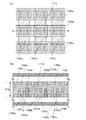
図1(A)は、第1の基板200と第2の基板201とが、ブルー相を示す液晶材料を用いた液晶層208を間に挟持して対向するように配置された液晶表示装置である。第1の基板200と液晶層208との間には第1の構造体233a、233b、画素電極層230a、230b、及び第2の共通電極層232a、232b、232cが設けられており、第2の基板201と液晶層208との間には第1の共通電極層231a、231b、231cが形成されている。第1の構造体233a、233bは第1の基板200の液晶層208側の面から液晶層208中に突出して設けられている。
FIG. 1A illustrates a liquid crystal display device in which a
第2の共通電極層232a、232b、232cは第1の基板200上、第1の共通電極層231a、231b、231cは第2の基板201上にそれぞれ形成され、液晶層208を介して対向するように配置される。第1の共通電極層231a、231b、231c及び第2の共通電極層232a、232b、232cは少なくとも画素領域において同形状であり液晶層を介して重畳するように配置されると、画素の開口率を低下させないために好ましい。
The second
画素電極層230a、230bは第1の基板200上に設けられた第1の構造体233a、233b上に形成され、液晶層208の膜厚方向において画素電極層230a、230bは第1の共通電極層231a、231b、231cと第2の共通電極層232a、232b、232cとの間に配置される。また、図1の断面図において、第1の共通電極層231a、231b、231c及び第2の共通電極層232a、232b、232cと、画素電極層230a、230bとは重畳せず互い違いに設けられている。
The pixel electrode layers 230 a and 230 b are formed over the
画素電極層(230a、230bを含む)、第1の共通電極層(231a、231b、231cを含む)及び第2の共通電極層(232a、232b、232cを含む)は平板状ではなく、開口パターンを有する形状であるために、断面図においては分断された複数の電極層として示される。 The pixel electrode layer (including 230a and 230b), the first common electrode layer (including 231a, 231b, and 231c) and the second common electrode layer (including 232a, 232b, and 232c) are not flat and have an opening pattern. In the cross-sectional view, it is shown as a plurality of divided electrode layers.
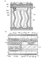
画素電極層が第1の共通電極層と第2の共通電極層との間に配置されるのであれば、第1の共通電極層及び第2の共通電極層も構造体上に形成してもよい。図1(B)は、第1の共通電極層231a、231b、231cと第2の基板201との間に第2の構造体234a、234b、234cが設けられる例である。第2の構造体234a、234b、234cは第2の基板201の液晶層208側の面から液晶層208中に突出して設けられている。
If the pixel electrode layer is disposed between the first common electrode layer and the second common electrode layer, the first common electrode layer and the second common electrode layer may also be formed on the structure. Good. FIG. 1B illustrates an example in which
また、図1(C)は、さらに第2の共通電極層232a、232b、232c下に第3の構造体235a、235b、235cが設けられる例である。第3の構造体235a、235b、235cは第1の基板200の液晶層208側の面から液晶層208中に突出して設けられている。この場合、同じ第1の基板200上に形成される画素電極層230a、230b及び第2の共通電極層232a、232b、232cにおいて、下に形成される構造体の高さは、画素電極層230a、230b下の第1の構造体233a、233bの方が、第2の共通電極層232a、232b、232c下の第3の構造体235a、235b、235cより高い。このように構造体の厚さ(高さ)や、数を制御することによって、第1の共通電極層、第2の共通電極層、及び画素電極層の液晶層中における配置位置を設定することができる。
FIG. 1C illustrates an example in which
液晶表示装置において液晶層の厚さであるセルギャップ(Dcg)は5μm未満(好ましくは1μm以上)とする。なお、本明細書においてセルギャップの厚さとは、液晶層の厚さ(膜厚)の最大値とする。よって、図1(A)乃至(C)においてセルギャップ(Dcg)は矢印で示す第1の基板200と第2の基板201との距離となる。
In the liquid crystal display device, the cell gap (Dcg) which is the thickness of the liquid crystal layer is less than 5 μm (preferably 1 μm or more). In the present specification, the thickness of the cell gap is the maximum value of the thickness (film thickness) of the liquid crystal layer. Therefore, in FIGS. 1A to 1C, the cell gap (Dcg) is a distance between the
セルギャップの厚さ(液晶層の厚さ)は第1の基板及び第2の基板間隔を保持するスペーサやシール材によって制御することができる。セルギャップの厚さ(液晶層の厚さ)を5μm未満とするため、液晶層中に設けられる画素電極層、第1の共通電極層、第2の共通電極層、及び構造体の膜厚も5μm未満となる。 The thickness of the cell gap (the thickness of the liquid crystal layer) can be controlled by a spacer or a sealing material that holds the distance between the first substrate and the second substrate. Since the thickness of the cell gap (the thickness of the liquid crystal layer) is less than 5 μm, the pixel electrode layer, the first common electrode layer, the second common electrode layer, and the thickness of the structure provided in the liquid crystal layer are also It becomes less than 5 μm.
図1(A)(B)(C)の液晶表示装置において、開口パターンを有し、かつ液晶を挟持するように設けられた画素電極層230a、230bと、第1の共通電極層231a、231b、231c及び第2の共通電極層232a、232b、232cとの間に電界を加えることで、液晶層208には斜め方向(基板に対して斜めの方向)の電界が加わるため、その電界を用いて液晶分子を制御できる。また画素電極層230a、230bは液晶層208の膜厚方向において、第1の共通電極層231a、231b、231cと第2の共通電極層232a、232b、232cとの間に配置されているため、液晶には画素電極層230a、230bと第1の共通電極層231a、231b、231cとの電界、及び画素電極層230a、230bと第2の共通電極層232a、232b、232cとの電界を加えることができ、液晶層全体に電界を形成することができる。
In the liquid crystal display device of FIGS. 1A, 1B, and 1C,
例えば、図1(A)(B)(C)においては画素電極層230aと第1の共通電極層231aとの間に矢印202aに示す斜め方向の電界が、画素電極層230aと第1の共通電極層231bとの間に矢印202bに示す斜め方向の電界が、画素電極層230aと第2の共通電極層232aとの間に矢印202cに示す斜め方向の電界が、画素電極層230aと第2の共通電極層232bとの間に矢印202dに示す斜め方向の電界がそれぞれ加わる。また、第1の共通電極層231a、231bと第2の基板201との間に第2の構造体234a、234b、第2の共通電極層232a、232bと第1の基板200との間に第3の構造体235a、235bを設ける構成であっても、電位線は円状に回り込むため、液晶層全体に電界が形成される。
For example, in FIGS. 1A, 1B, and 1C, an oblique electric field indicated by an
構造体上に設けられ、液晶層中において、第1の共通電極層及び第2の共通電極層の間に配置された画素電極層と、第2の基板に設けられた第1の共通電極層及び第1の基板に設けられた第2の共通電極層それぞれと斜め電界を形成することによって、液晶層全体に斜め電界を形成することが可能となる。 A pixel electrode layer provided on the structure and disposed between the first common electrode layer and the second common electrode layer in the liquid crystal layer, and a first common electrode layer provided on the second substrate By forming an oblique electric field with each of the second common electrode layers provided on the first substrate, an oblique electric field can be formed on the entire liquid crystal layer.
従って、膜厚方向も含め液晶層全体における液晶分子を応答させることができ、白透過率が向上する。よって白透過率と黒透過率(黒表示時の光の透過率)との比であるコントラスト比も高くすることができる。 Accordingly, liquid crystal molecules in the entire liquid crystal layer including the film thickness direction can be caused to respond, and white transmittance is improved. Therefore, the contrast ratio, which is the ratio between the white transmittance and the black transmittance (light transmittance during black display), can also be increased.
また、比較的粘度の高いブルー相を示す液晶材料においても、より低電圧で効果的に電界を印加することができるため、液晶表示装置の低消費電力化も達成できる。 In addition, even in a liquid crystal material exhibiting a relatively high-viscosity blue phase, an electric field can be effectively applied at a lower voltage, so that the power consumption of the liquid crystal display device can be reduced.
構造体は絶縁性材料(有機材料及び無機材料)を用いた絶縁体、及び導電性材料(有機材料及び無機材料)を用いた導電体で形成することができる。代表的には可視光硬化性、紫外線硬化性または熱硬化性の樹脂を用いるのが好ましい。例えば、アクリル樹脂、エポキシ樹脂、アミン樹脂などを用いることができる。また、導電性樹脂や金属材料で形成してもよい。なお、構造体は複数の薄膜の積層構造であってもよい。構造体の形状は、柱状、錐形の先端が平面である断面が台形の形状、錐形の先端が丸いドーム状などを用いることができる。また、構造体は基板の液晶層側の面から液晶層中に突出する部分であればよいので、層間膜を加工して液晶層側の表面を凹凸形状とし、突出する構造体としてもよい。よって、構造体は複数の突出した凸部を有する連続膜であってもよい。 The structure can be formed using an insulator using an insulating material (organic material and inorganic material) and a conductor using a conductive material (organic material and inorganic material). Typically, it is preferable to use a visible light curable resin, an ultraviolet curable resin, or a thermosetting resin. For example, an acrylic resin, an epoxy resin, an amine resin, or the like can be used. Moreover, you may form with a conductive resin or a metal material. Note that the structure may be a stacked structure of a plurality of thin films. As the shape of the structure, a columnar shape, a trapezoidal shape in which the tip of the cone is flat, or a dome shape in which the tip of the cone is round can be used. In addition, since the structure body may be a portion that protrudes into the liquid crystal layer from the surface on the liquid crystal layer side of the substrate, the interlayer film may be processed to make the surface on the liquid crystal layer side uneven, thereby projecting the structure body. Therefore, the structure may be a continuous film having a plurality of protruding protrusions.
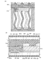
なお、構造体上に形成される画素電極層、第1の共通電極層及び第2の共通電極層の形状は、該構造体の形状が反映され、またエッチング加工方法にも影響をうける。構造体及び該構造体上に形成される画素電極層の形状例を図19(A)(B)に示す。なお、図19では第1の構造体及び画素電極層を例として示すが、第2の構造体及び第1の共通電極層と、第3の構造体及び第2の共通電極層も同様に様々な形状を適用することができる。 Note that the shapes of the pixel electrode layer, the first common electrode layer, and the second common electrode layer formed over the structure reflect the shape of the structure, and the etching method is also affected. FIGS. 19A and 19B show examples of the shape of the structure and the pixel electrode layer formed over the structure. Note that although FIG. 19 illustrates the first structure body and the pixel electrode layer as an example, the second structure body and the first common electrode layer, and the third structure body and the second common electrode layer are similarly various. Various shapes can be applied.
図19(A)は、第1の構造体241a、241b上に画素電極層240a、240bがそれぞれ形成される例であり、図19(B)は、第1の構造体243a、243b上に画素電極層242a、242bがそれぞれ形成される例である。第1の構造体241a、241b、243a、243bは錐形の先端が丸いドーム形状の構造体である。第1の構造体241a、241b上に設けられた画素電極層240a、240bは、第1の構造体241a、241b側面を覆うように形成され、部分的に第1の基板200に接している例である。一方、第1の構造体243a、243b上に設けられた画素電極層242a、242bは第1の構造体243a、243bの側面上方部分にのみ形成されている例である。このように画素電極層が構造体側面(全部、又は部分的に)を覆う形状であってもよいし、画素電極層が不均一な膜厚分布を有していてもよい。この場合でも、液晶層において画素電極層は第1の共通電極層と第2の共通電極層の間に存在する領域を有するため、第1の共通電極層及び第2の共通電極層と斜め電界を液晶層全体にわたって形成する効果を奏する。よって、画素電極層は少なくとも液晶の厚さ方向の該画素電極層の最も高い位置(画素電極層の上面)において、第1の共通電極層及び第2の共通電極層の間に配置されるものとする。
FIG. 19A illustrates an example in which
液晶層208を形成する方法として、ディスペンサ法(滴下法)や、第1の基板200と第2の基板201とを貼り合わせてから毛細管現象を用いて液晶を注入する注入法を用いることができる。
As a method for forming the
液晶層208には、ブルー相を示す液晶材料を用いる。ブルー相を示す液晶材料は、応答速度が1msec以下と短く高速応答が可能であるため、液晶表示装置の高性能化が可能になる。
A liquid crystal material exhibiting a blue phase is used for the
ブルー相を示す液晶材料として液晶及びカイラル剤を含む。カイラル剤は、液晶を螺旋構造に配向させ、ブルー相を発現させるために用いる。例えば、数重量%以上のカイラル剤を混合させた液晶材料を液晶層に用いればよい。 A liquid crystal material exhibiting a blue phase includes a liquid crystal and a chiral agent. The chiral agent is used to align the liquid crystal in a spiral structure and develop a blue phase. For example, a liquid crystal material mixed with several percent by weight or more of a chiral agent may be used for the liquid crystal layer.
液晶は、サーモトロピック液晶、低分子液晶、高分子液晶、強誘電液晶、反強誘電液晶等を用いる。 As the liquid crystal, a thermotropic liquid crystal, a low molecular liquid crystal, a polymer liquid crystal, a ferroelectric liquid crystal, an antiferroelectric liquid crystal, or the like is used.
カイラル剤は、液晶に対する相溶性が良く、かつ捩れ力の強い材料を用いる。また、R体、S体のどちらか片方の材料が良く、R体とS体の割合が50:50のラセミ体は使用しない。 As the chiral agent, a material having a good compatibility with liquid crystal and a strong twisting force is used. Also, either the R-form or the S-form is good, and a racemate with a ratio of R-form to S-form of 50:50 is not used.
上記液晶材料は、条件により、コレステリック相、コレステリックブルー相、スメクチック相、スメクチックブルー相、キュービック相、カイラルネマチック相、等方相等を示す。 The liquid crystal material exhibits a cholesteric phase, a cholesteric blue phase, a smectic phase, a smectic blue phase, a cubic phase, a chiral nematic phase, an isotropic phase, or the like depending on conditions.
ブルー相であるコレステリックブルー相及びスメクチックブルー相は、螺旋ピッチが500nm以下とピッチの比較的短いコレステリック相またはスメクチック相を有する液晶材料にみられる。液晶材料の配向は二重ねじれ構造を有する。可視光の波長以下の秩序を有しているため、透明であり、電圧印加によって配向秩序が変化して光学的変調作用が生じる。ブルー相は光学的に等方であるため視野角依存性がなく、配向膜を形成しなくとも良いため、表示画像の質の向上及びコスト削減が可能である。 A cholesteric blue phase and a smectic blue phase, which are blue phases, are found in liquid crystal materials having a cholesteric phase or a smectic phase with a relatively short helical pitch of 500 nm or less. The alignment of the liquid crystal material has a double twisted structure. Since it has an order equal to or less than the wavelength of visible light, it is transparent, and the alignment order is changed by application of a voltage to cause an optical modulation action. Since the blue phase is optically isotropic, it does not depend on the viewing angle, and it is not necessary to form an alignment film, so that the quality of the display image can be improved and the cost can be reduced.
また、ブルー相は狭い温度範囲でしか発現が難しく、温度範囲を広く改善するために液晶材料に、光硬化樹脂及び光重合開始剤を添加し、高分子安定化処理を行うことが好ましい。高分子安定化処理は、液晶、カイラル剤、光硬化樹脂、及び光重合開始剤を含む液晶材料に、光硬化樹脂、及び光重合開始剤が反応する波長の光を照射して行う。この高分子安定化処理は、温度制御を行い、等方相を示した状態で光照射して行っても良いし、ブルー相を示した状態で光照射して行ってもよい。 In addition, the blue phase is difficult to develop only in a narrow temperature range, and in order to improve the temperature range widely, it is preferable to add a photocurable resin and a photopolymerization initiator to the liquid crystal material and perform polymer stabilization treatment. The polymer stabilization treatment is performed by irradiating a liquid crystal material including a liquid crystal, a chiral agent, a photocuring resin, and a photopolymerization initiator with light having a wavelength at which the photocuring resin and the photopolymerization initiator react. This polymer stabilization treatment may be performed by temperature control and light irradiation in a state showing an isotropic phase, or by light irradiation in a state showing a blue phase.
例えば、液晶層の温度を制御し、ブルー相を発現した状態で液晶層に光を照射することにより高分子安定化処理を行う。但し、これに限定されず、ブルー相と等方相間の相転移温度から+10℃以内、好ましくは+5℃以内の等方相を発現した状態で液晶層に光を照射することにより高分子安定化処理を行ってもよい。ブルー相と等方相間の相転移温度とは、昇温時にブルー相から等方相に転移する温度又は降温時に等方相からブルー相に相転移する温度をいう。高分子安定化処理の一例としては、液晶層を等方相まで加熱した後、徐々に降温させてブルー相にまで相転移させ、ブルー相が発現する温度を保持した状態で光を照射することができる。他にも、液晶層を徐々に加熱して等方相に相転移させた後、ブルー相と等方相間の相転移温度から+10℃以内、好ましくは+5℃以内の状態(等方相を発現した状態)で光を照射することができる。また、液晶材料に含まれる光硬化樹脂として、紫外線硬化樹脂(UV硬化樹脂)を用いる場合、液晶層に紫外線を照射すればよい。なお、ブルー相を発現させなくとも、ブルー相と等方相間の相転移温度から+10℃以内、好ましくは+5℃以内の状態(等方相を発現した状態)で光を照射して高分子安定化処理を行えば、応答速度が1msec以下と短く高速応答が可能である。 For example, the polymer stabilization treatment is performed by controlling the temperature of the liquid crystal layer and irradiating the liquid crystal layer with light in a state where a blue phase is developed. However, the present invention is not limited to this, and the polymer is stabilized by irradiating the liquid crystal layer with light in a state where the isotropic phase is expressed within + 10 ° C, preferably within + 5 ° C from the phase transition temperature between the blue phase and the isotropic phase. Processing may be performed. The phase transition temperature between the blue phase and the isotropic phase refers to a temperature at which the blue phase is changed to the isotropic phase when the temperature is raised or a temperature at which the isotropic phase is changed to the blue phase when the temperature is lowered. As an example of the polymer stabilization treatment, after the liquid crystal layer is heated to an isotropic phase, the temperature is gradually lowered to a phase transition to the blue phase, and light is irradiated while maintaining the temperature at which the blue phase appears. Can do. In addition, after the liquid crystal layer is gradually heated to change into the isotropic phase, it is within + 10 ° C, preferably within + 5 ° C from the phase transition temperature between the blue phase and the isotropic phase (expressing the isotropic phase) Can be irradiated with light. In addition, when an ultraviolet curable resin (UV curable resin) is used as a photocurable resin included in the liquid crystal material, the liquid crystal layer may be irradiated with ultraviolet rays. Even if the blue phase is not expressed, the polymer is stable by irradiating light within + 10 ° C, preferably within + 5 ° C from the phase transition temperature between the blue phase and the isotropic phase (the state where the isotropic phase is expressed). If the processing is performed, a high-speed response is possible with a response speed as short as 1 msec or less.
光硬化樹脂は、アクリレート、メタクリレートなどの単官能モノマーでもよく、ジアクリレート、トリアクリレート、ジメタクリレート、トリメタクリレートなどの多官能モノマーでもよく、これらを混合させたものでもよい。また、液晶性のものでも非液晶性のものでもよく、両者を混合させてもよい。光硬化樹脂は、用いる光重合開始剤の反応する波長の光で硬化する樹脂を選択すれば良く、代表的には紫外線硬化樹脂を用いることができる。 The photocurable resin may be a monofunctional monomer such as acrylate or methacrylate, may be a polyfunctional monomer such as diacrylate, triacrylate, dimethacrylate, or trimethacrylate, or may be a mixture of these. Further, it may be liquid crystalline or non-liquid crystalline, and both may be mixed. The photo-curing resin may be selected from a resin that cures with light having a wavelength with which the photopolymerization initiator to be used reacts. Typically, an ultraviolet-curing resin can be used.
光重合開始剤は、光照射によってラジカルを発生させるラジカル重合開始剤でもよく、酸を発生させる酸発生剤でもよく、塩基を発生させる塩基発生剤でもよい。 The photopolymerization initiator may be a radical polymerization initiator that generates radicals by light irradiation, an acid generator that generates acid, or a base generator that generates a base.
具体的には、液晶材料として、JC−1041XX(チッソ株式会社製)と4−シアノ−4’−ペンチルビフェニルの混合物を用いることができ、カイラル剤としては、ZLI−4572(メルク株式会社製)を用いることができ、光硬化樹脂は、2−エチルヘキシルアクリレート、RM257(メルク株式会社製)、トリメチロールプロパントリアクリレートを用いることができ、光重合開始剤としては2,2−ジメトキシ−2−フェニルアセトフェノンを用いることができる。 Specifically, as a liquid crystal material, a mixture of JC-1041XX (manufactured by Chisso Corporation) and 4-cyano-4′-pentylbiphenyl can be used, and as a chiral agent, ZLI-4572 (manufactured by Merck Corporation). 2-ethylhexyl acrylate, RM257 (manufactured by Merck & Co., Inc.), trimethylolpropane triacrylate can be used as the photocurable resin, and 2,2-dimethoxy-2-phenyl is used as the photopolymerization initiator. Acetophenone can be used.
また、図1では図示しないが、偏光板、位相差板、反射防止膜などの光学フィルムなどは適宜設ける。例えば、偏光板及び位相差板による円偏光を用いてもよい。また、光源としてバックライトなどを用いることができる。 Although not shown in FIG. 1, an optical film such as a polarizing plate, a retardation plate, and an antireflection film is provided as appropriate. For example, circularly polarized light using a polarizing plate and a retardation plate may be used. Further, a backlight or the like can be used as the light source.
本明細書において、液晶表示装置は光源の光を透過することによって表示を行う透過型の液晶表示装置である(又は半透過型の液晶表示装置)場合、少なくとも画素領域において光を透過させる必要がある。よって光が透過する画素領域に存在する第1の基板、第2の基板、絶縁膜、導電膜などの薄膜はすべて可視光の波長領域の光に対して透光性とする。 In this specification, in the case where the liquid crystal display device is a transmissive liquid crystal display device that performs display by transmitting light from a light source (or a transflective liquid crystal display device), it is necessary to transmit light at least in a pixel region. is there. Therefore, thin films such as the first substrate, the second substrate, the insulating film, and the conductive film existing in the pixel region where light is transmitted have light-transmitting properties with respect to light in the visible wavelength region.
画素電極層、第1の共通電極層及び第2の共通電極層においては透光性が好ましいが、開口パターンを有するために金属膜などの非透光性材料を用いてもよい。 The pixel electrode layer, the first common electrode layer, and the second common electrode layer are preferably translucent, but a non-translucent material such as a metal film may be used to have an opening pattern.
画素電極層、第1の共通電極層及び第2の共通電極層は、インジウム錫酸化物(ITO)、酸化インジウムに酸化亜鉛(ZnO)を混合したIZO(indium zinc oxide)、酸化インジウムに酸化珪素(SiO2)を混合した導電材料、有機インジウム、有機スズ、酸化タングステンを含むインジウム酸化物、酸化タングステンを含むインジウム亜鉛酸化物、酸化チタンを含むインジウム酸化物、酸化チタンを含むインジウム錫酸化物、またはタングステン(W)、モリブデン(Mo)、ジルコニウム(Zr)、ハフニウム(Hf)、バナジウム(V)、ニオブ(Nb)、タンタル(Ta)、クロム(Cr)、コバルト(Co)、ニッケル(Ni)、チタン(Ti)、白金(Pt)、アルミニウム(Al)、銅(Cu)、銀(Ag)等の金属、又はその合金、若しくはその金属窒化物から一つ、又は複数種を用いて形成することができる。 The pixel electrode layer, the first common electrode layer, and the second common electrode layer are made of indium tin oxide (ITO), indium oxide and zinc oxide (ZnO), indium zinc oxide (IZO), and indium oxide in silicon oxide. (SiO 2 ) mixed conductive material, organic indium, organic tin, indium oxide containing tungsten oxide, indium zinc oxide containing tungsten oxide, indium oxide containing titanium oxide, indium tin oxide containing titanium oxide, Or tungsten (W), molybdenum (Mo), zirconium (Zr), hafnium (Hf), vanadium (V), niobium (Nb), tantalum (Ta), chromium (Cr), cobalt (Co), nickel (Ni) , Titanium (Ti), platinum (Pt), aluminum (Al), copper (Cu), silver ( It can be formed from one or more kinds of metals such as Ag), alloys thereof, or metal nitrides thereof.
第1の基板200、第2の基板201にはバリウムホウケイ酸ガラスやアルミノホウケイ酸ガラスなどのガラス基板、石英基板、プラスチック基板などを用いることができる。
As the
以上のように、ブルー相を示す液晶層を用いた液晶表示装置において、コントラスト比を高めることができる。 As described above, in a liquid crystal display device using a liquid crystal layer exhibiting a blue phase, the contrast ratio can be increased.
また、より低電圧で高い白透過率を得ることができるため、液晶表示装置の低消費電力化も達成できる。 Further, since a high white transmittance can be obtained at a lower voltage, the power consumption of the liquid crystal display device can be reduced.
(実施の形態2)
本明細書に開示する発明は、パッシブマトリクス型の液晶表示装置でもアクティブマトリクス型の液晶表示装置にも適用することができる。アクティブマトリクス型の液晶表示装置の例を、図2、図8及び図18を用いて説明する。
(Embodiment 2)
The invention disclosed in this specification can be applied to either a passive matrix liquid crystal display device or an active matrix liquid crystal display device. An example of an active matrix liquid crystal display device will be described with reference to FIGS.
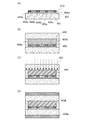
図2(A)は液晶表示装置の平面図であり1画素分の画素を示している。図2(B)は図2(A)の線X1−X2における断面図である。 FIG. 2A is a plan view of the liquid crystal display device and shows one pixel. FIG. 2B is a cross-sectional view taken along line X1-X2 in FIG.
図2(A)において、複数のソース配線層(配線層405aを含む)が互いに平行(図中上下方向に延伸)かつ互いに離間した状態で配置されている。複数のゲート配線層(ゲート電極層401を含む)は、ソース配線層に概略直交する方向(図中左右方向)に延伸し、かつ互いに離間するように配置されている。容量配線層408は、複数のゲート配線層それぞれに隣接する位置に配置されており、ゲート配線層に概略平行な方向、つまり、ソース配線層に概略直交する方向(図中左右方向)に延伸している。ソース配線層と、容量配線層408及びゲート配線層とによって、概略長方形の空間が囲まれているが、この空間に液晶表示装置の画素電極層、第1の共通電極層及び第2の共通電極層が液晶層444を介して配置されている。画素電極層を駆動するトランジスタ420は、図中左上の角に配置されている。画素電極層及びトランジスタは、マトリクス状に複数配置されている。
In FIG. 2A, a plurality of source wiring layers (including the
図2の液晶表示装置において、トランジスタ420に電気的に接続する第1の電極層447が画素電極層として機能し、第2の電極層446が第1の共通電極層、第3の電極層448が第2の共通電極層として機能する。なお、第1の電極層447と容量配線層408によって容量が形成されている。第1の共通電極層及び第2の共通電極層とはフローティング状態(電気的に孤立した状態)として動作させることも可能だが、固定電位、好ましくはコモン電位(データとして送られる画像信号の中間電位)近傍でフリッカーの生じないレベルに設定してもよい。なお、第1の共通電極層及び第2の共通電極層は等電位が好ましい。
In the liquid crystal display device in FIG. 2, the
画素電極層である第1の電極層447は第1の基板441(素子基板ともいう)上の層間膜413の液晶層444側の面から液晶層444に突出して設けられた第1の構造体449上に形成され、液晶層444の膜厚方向において画素電極層である第1の電極層447は第1の共通電極層である第2の電極層446と第2の共通電極層である第3の電極層448との間に配置される。また、図2(B)の断面図において、第1の電極層447と、第2の電極層446及び第3の電極層448とは重畳せず互い違いに設けられている。第2の電極層446及び第3の電極層448は少なくとも画素領域において同形状であり液晶層444を介して重畳するように配置されると、画素の開口率を低下させないために好ましい。
The
液晶表示装置において液晶層の厚さであるセルギャップ(Dcg)は5μm未満(好ましくは1μm以上)とする。なお、本明細書においてセルギャップの厚さとは、液晶層の厚さ(膜厚)の最大値とする。よって、図2(B)においてセルギャップ(Dcg)は矢印で示す層間膜413と第2の基板442との距離となる。
In the liquid crystal display device, the cell gap (Dcg) which is the thickness of the liquid crystal layer is less than 5 μm (preferably 1 μm or more). In the present specification, the thickness of the cell gap is the maximum value of the thickness (film thickness) of the liquid crystal layer. Therefore, in FIG. 2B, the cell gap (Dcg) is a distance between the
セルギャップの厚さ(液晶層の厚さ)は層間膜413及び第2の基板442の間隔を保持するスペーサやシール材によって制御することができる。セルギャップの厚さ(液晶層の厚さ)を5μm未満とするため、液晶層中に設けられる画素電極層、第1の共通電極層、第2の共通電極層、及び構造体の膜厚も5μm未満となる。
The thickness of the cell gap (the thickness of the liquid crystal layer) can be controlled by a spacer or a sealant that keeps the distance between the
第1の電極層447、第2の電極層446及び第3の電極層448は平板状ではなく、様々な開口パターンを有し、屈曲部や枝分かれした櫛歯状を含む形状である。
The
第1の電極層447が第2の電極層446と第3の電極層448との間に配置されるのであれば、実施の形態1で示したように第2の電極層446及び第3の電極層448とも液晶層中に突出して設けられた構造体上に形成してもよい。
If the
開口パターンを有し、かつ液晶を挟持するように設けられた第1の電極層447と、第2の電極層446及び第3の電極層448との間に電界を加えることで、液晶層444には斜め方向(基板に対して斜めの方向)の電界が加わるため、その電界を用いて液晶分子を制御できる。また第1の電極層447は液晶層444の膜厚方向において、第2の電極層446と第3の電極層448との間に配置されているため、液晶には第1の電極層447と第2の電極層446との電界、及び第1の電極層447と第3の電極層448との電界を加えることができ、液晶層444全体に電界を形成することができる。
By applying an electric field between the
従って、液晶層444全体に形成された斜め電界によって、膜厚方向も含め液晶層全体における液晶分子を応答させることができ、白透過率が向上する。よって白透過率と黒透過率(黒表示時の光の透過率)との比であるコントラスト比も高くすることができる。
Therefore, liquid crystal molecules in the entire liquid crystal layer including the film thickness direction can be caused to respond by an oblique electric field formed in the entire
構造体は絶縁性材料(有機材料及び無機材料)を用いた絶縁体、及び導電性材料(有機材料及び無機材料)を用いた導電体で形成することができる。代表的には可視光硬化性、紫外線硬化性または熱硬化性の樹脂を用いるのが好ましい。例えば、アクリル樹脂、エポキシ樹脂、アミン樹脂などを用いることができる。また、導電性樹脂や金属材料で形成してもよい。なお、構造体は複数の薄膜の積層構造であってもよい。構造体の形状は、柱状、錐形の先端が平面である断面が台形の形状、錐形の先端が丸いドーム状などを用いることができる。また、構造体は基板の液晶層側の面から液晶層中に突出する部分であればよいので、層間膜を加工して液晶層側の表面を凹凸形状とし、突出する構造体としてもよい。よって、構造体は複数の突出した凸部を有する連続膜であってもよい。 The structure can be formed using an insulator using an insulating material (organic material and inorganic material) and a conductor using a conductive material (organic material and inorganic material). Typically, it is preferable to use a visible light curable resin, an ultraviolet curable resin, or a thermosetting resin. For example, an acrylic resin, an epoxy resin, an amine resin, or the like can be used. Moreover, you may form with a conductive resin or a metal material. Note that the structure may be a stacked structure of a plurality of thin films. As the shape of the structure, a columnar shape, a trapezoidal shape in which the tip of the cone is flat, or a dome shape in which the tip of the cone is round can be used. In addition, since the structure body may be a portion that protrudes into the liquid crystal layer from the surface on the liquid crystal layer side of the substrate, the interlayer film may be processed to make the surface on the liquid crystal layer side uneven, thereby projecting the structure body. Therefore, the structure may be a continuous film having a plurality of protruding protrusions.
構造体の形成方法は特に限定されず、材料に応じて、蒸着法、スパッタ法、CVD法などの乾式法、又はスピンコート、ディップ、スプレー塗布、液滴吐出法(インクジェット法)、ナノインプリント、各種印刷法(スクリーン印刷、オフセット印刷)等などの湿式法を用い、必要に応じてエッチング法(ドライエッチング又はウエットエッチング)により所望のパターンに加工すればよい。 The method for forming the structure is not particularly limited, and depending on the material, a dry method such as a vapor deposition method, a sputtering method, or a CVD method, or spin coating, dipping, spray coating, a droplet discharge method (inkjet method), nanoimprint, various types A wet method such as a printing method (screen printing, offset printing) or the like may be used, and a desired pattern may be processed by an etching method (dry etching or wet etching) as necessary.
図2(B)のように、第1の電極層447が形成される構造体449は、端部に曲率を有するテーパー形状であると第1の電極層447の被膜性が向上するために好ましい。本実施の形態では、第1の電極層447はトランジスタ420の配線層405bと接し、構造体449上にまで連続的に成膜される例であるが、配線層405bと接する電極層を形成し、その電極層を介して第1の電極層447を形成してもよい。
As shown in FIG. 2B, the
また、トランジスタを覆って層間膜を形成し、層間膜上に構造体を形成する場合、構造体をエッチング加工によって形成した後、層間膜にトランジスタと接続するためのコンタクトホールを開口してもよい。なお図2は、層間膜及び構造体となる絶縁膜にコンタクトホールを形成した後、絶縁膜をエッチング加工して構造体を形成する例である。 In the case where an interlayer film is formed so as to cover the transistor and a structure is formed over the interlayer film, a contact hole for connecting to the transistor may be opened in the interlayer film after the structure is formed by etching. . FIG. 2 shows an example in which a contact hole is formed in an interlayer film and an insulating film to be a structure, and then the insulating film is etched to form a structure.
第1の電極層447、第2の電極層446、及び第3の電極層448の他の例を図8に示す。図中では省略しているが第1の電極層447と第2の電極層446とは液晶層444を間に挟持しており、第2の共通電極層である第3の電極層448は第1の共通電極層である第2の電極層446と対向して配置されている。図8(A)乃至(D)の上面図に示すように、第1の電極層447a乃至447d及び第2の電極層446a乃至446dが互い違いとなるように形成されており、図8(A)では第1の電極層447a及び第2の電極層446aはうねりを有する波状形状であり、図8(B)では第1の電極層447b及び第2の電極層446bは同心円状の開口部を有する形状であり、図8(C)では第1の電極層447c及び第2の電極層446cは櫛歯状であり一部重なっている形状であり、図8(D)では第1の電極層447d及び第2の電極層446dは櫛歯状であり電極同士がかみ合うような形状である。
Another example of the
なお、図8(A)乃至(C)のように、第1の電極層447a、447b、447c、と第3の電極層448a、448b、448cとが重なる場合は、第1の電極層447と第3の電極層448との間には絶縁膜を形成し、異なる膜上に第1の電極層447と第3の電極層448とを形成する。
Note that in the case where the
図18の液晶表示装置は、図18(B)の断面図に示すように、画素電極層である第1の電極層447と、第2の共通電極層である第3の電極層448とが別の膜上(別レイヤー上)にそれぞれ設けられている。
As shown in the cross-sectional view of FIG. 18B, the liquid crystal display device in FIG. 18 includes a
図18においては、第2の共通電極層である第3の電極層448が層間膜413上に形成されており、第3の電極層448上には絶縁膜416が積層され、絶縁膜416上に画素電極層である第1の電極層447が形成されている。なお、図18においては、第1の電極層と共通配線層とによって容量が形成されている。
In FIG. 18, a
トランジスタ420は逆スタガ型の薄膜トランジスタであり、絶縁表面を有する基板である第1の基板441上に、ゲート電極層401、ゲート絶縁層402、半導体層403、ソース電極層又はドレイン電極層として機能する配線層405a、405bを含む。
The
トランジスタ420を覆い、半導体層403に接する絶縁膜407が設けられている。絶縁膜407上に層間膜413が設けられ、層間膜413上に第1の電極層447が形成され、液晶層444を介して第2の電極層446が形成されている。
An insulating
液晶表示装置にカラーフィルタ層として機能する着色層を設けることができる。カラーフィルタ層は、第1の基板441及び第2の基板442より外側(液晶層444と反対側)に設けてもよいし、第1の基板441及び第2の基板442より内側に設けてもよい。
A colored layer that functions as a color filter layer can be provided in the liquid crystal display device. The color filter layer may be provided on the outer side (opposite side to the liquid crystal layer 444) than the
カラーフィルタは、液晶表示装置をフルカラー表示とする場合、赤色(R)、緑色(G)、青色(B)を呈する材料から形成すればよく、モノカラー表示とする場合、着色層を無くす、もしくは少なくとも一つの色を呈する材料から形成すればよい。なお、バックライト装置にRGBの発光ダイオード(LED)等を配置し、時分割によりカラー表示する継時加法混色法(フィールドシーケンシャル法)を採用するときには、カラーフィルタを設けない場合もある。 The color filter may be formed from a material exhibiting red (R), green (G), and blue (B) when the liquid crystal display device is set to full color display. What is necessary is just to form from the material which exhibits at least 1 color. Note that a color filter may not be provided when an RGB light-emitting diode (LED) or the like is arranged in the backlight device and a continuous additive color mixing method (field sequential method) in which color display is performed by time division is employed.
図2の液晶表示装置は、層間膜413に、カラーフィルタ層として機能する有彩色の透光性樹脂層417を用いる例である。
The liquid crystal display device in FIG. 2 is an example in which a chromatic
カラーフィルタ層を対向基板側に設ける場合、トランジスタが形成される素子基板との、正確な画素領域の位置合わせが難しく、画質を損なう恐れがあるが、層間膜をカラーフィルタ層として直接素子基板側に形成するのでより精密な形成領域の制御ができ、微細なパターンの画素にも対応することができる。また、層間膜とカラーフィルタ層を同一の絶縁層で兼ねるので、工程が簡略化し、より低コストで液晶表示装置を作製することができる。 When the color filter layer is provided on the counter substrate side, it is difficult to accurately align the pixel region with the element substrate on which the transistor is formed, and the image quality may be impaired. Therefore, it is possible to control the formation region more precisely and to deal with pixels with fine patterns. In addition, since the same insulating layer serves as the interlayer film and the color filter layer, the process can be simplified and a liquid crystal display device can be manufactured at a lower cost.
有彩色の透光性樹脂としては、感光性、非感光性の有機樹脂を用いることができる。感光性の有機樹脂層を用いるとレジストマスク数を削減することができるため、工程が簡略化し好ましい。また、層間膜に形成するコンタクトホールも曲率を有する開口形状となるために、コンタクトホールに形成される電極層などの膜の被覆性も向上させることができる。 As the chromatic translucent resin, a photosensitive or non-photosensitive organic resin can be used. The use of a photosensitive organic resin layer is preferable because the number of resist masks can be reduced and the process is simplified. In addition, since the contact hole formed in the interlayer film has an opening shape having a curvature, the coverage of a film such as an electrode layer formed in the contact hole can be improved.
有彩色は、黒、灰、白などの無彩色を除く色であり、着色層はカラーフィルタとして機能させるため、その着色された有彩色の光のみを透過する材料で形成される。有彩色としては、赤色、緑色、青色などを用いることができる。また、シアン、マゼンダ、イエロー(黄)などを用いてもよい。着色された有彩色の光のみを透過するとは、着色層において透過する光は、その有彩色の光の波長にピークを有するということである。 The chromatic color is a color excluding achromatic colors such as black, gray, and white, and the colored layer is formed of a material that transmits only the colored chromatic light in order to function as a color filter. As the chromatic color, red, green, blue, or the like can be used. Further, cyan, magenta, yellow (yellow), or the like may be used. To transmit only colored chromatic light means that light transmitted through the colored layer has a peak at the wavelength of the chromatic light.
有彩色の透光性樹脂層417は、着色層(カラーフィルタ)として機能させるため、含ませる着色材料の濃度と光の透過率の関係に考慮して、最適な膜厚を適宜制御するとよい。層間膜413を複数の薄膜で積層する場合、少なくとも一層が有彩色の透光性樹脂層であれば、カラーフィルタとして機能させることができる。
Since the chromatic
有彩色の色によって有彩色の透光性樹脂層の膜厚が異なる場合や、遮光層、トランジスタに起因する凹凸を有する場合は、可視光の波長領域の光を透過する(いわゆる無色透明)絶縁層を積層し、層間膜表面を平坦化してもよい。層間膜の平坦性を高めるとその上に形成される画素電極層や第2の共通電極層の被覆性もよく、かつ液晶層のギャップ(膜厚)を均一にすることができるため、より液晶表示装置の視認性を向上させ、高画質化が可能になる。 When the film thickness of the chromatic transparent resin layer differs depending on the chromatic color, or when the light shielding layer or the unevenness caused by the transistor is present, the light in the visible wavelength region is transmitted (so-called colorless and transparent). Layers may be stacked to planarize the interlayer film surface. When the flatness of the interlayer film is increased, the pixel electrode layer and the second common electrode layer formed thereon have good coverage, and the gap (film thickness) of the liquid crystal layer can be made uniform. The visibility of the display device can be improved and high image quality can be achieved.
層間膜413(有彩色の透光性樹脂層417)の形成法は、特に限定されず、その材料に応じて、スピンコート、ディップ、スプレー塗布、液滴吐出法(インクジェット法、スクリーン印刷、オフセット印刷等)等の方法、ドクターナイフ、ロールコーター、カーテンコーター、ナイフコーター等のツール(設備)を用いることができる。 The formation method of the interlayer film 413 (the chromatic color translucent resin layer 417) is not particularly limited, and spin coating, dip, spray coating, droplet discharge method (ink jet method, screen printing, offset) depending on the material. Printing, etc.) and tools (equipment) such as a doctor knife, roll coater, curtain coater, knife coater, etc. can be used.
第1の電極層447及び第3の電極層448上には液晶層444が設けられ、第2の電極層446が形成された対向基板である第2の基板442で封止されている。
A
第1の基板441及び第2の基板442は透光性基板であり、それぞれ外側(液晶層444と反対側)に偏光板443a、443bが設けられている。
The
図7(A)乃至(D)を用いて図2に示す液晶表示装置の作製工程を説明する。図7(A)乃至(D)は液晶表示装置の作製工程の断面図である。なお、図7(A)乃至(D)では含まれる画素電極層、第1の共通電極層及び第2の共通電極層は省略している。画素電極層、第1の共通電極層及び第2の共通電極層は図2の構造を用いることができ、液晶層において構造体上の画素電極層が第1の共通電極層及び第2の共通電極層間に配置されて生じる斜め電界モードを適用することができる。 A manufacturing process of the liquid crystal display device illustrated in FIG. 2 will be described with reference to FIGS. 7A to 7D are cross-sectional views illustrating a manufacturing process of a liquid crystal display device. Note that the pixel electrode layer, the first common electrode layer, and the second common electrode layer which are included in FIGS. 7A to 7D are omitted. The structure shown in FIG. 2 can be used for the pixel electrode layer, the first common electrode layer, and the second common electrode layer. In the liquid crystal layer, the pixel electrode layer on the structure is the first common electrode layer and the second common electrode layer. An oblique electric field mode generated between electrode layers can be applied.
図7(A)において、素子基板である第1の基板441上に素子層451が形成され、素子層451上に層間膜413が形成されている。
In FIG. 7A, an
層間膜413は、有彩色の透光性樹脂層454a、454b、454c及び遮光層455a、455b、455c、455dを含み、遮光層455a、455b、455c、455dの間に有彩色の透光性樹脂層454a、454b、454cがそれぞれ形成される構成である。なお、図7(A)乃至(D)では含まれる画素電極層、第1の共通電極層及び第2の共通電極層は省略している。
The
図7(B)に示すように、第1の基板441と対向基板である第2の基板442とを、液晶層458を間に挟持させてシール材456a、456bで固着する。液晶層458を形成する方法として、ディスペンサ法(滴下法)や、第1の基板441と第2の基板442とを貼り合わせてから毛細管現象を用いて液晶を注入する注入法を用いることができる。
As shown in FIG. 7B, the
液晶層458には、ブルー相を示す液晶材料を用いることができる。液晶層458は、液晶、カイラル剤、光硬化樹脂、及び光重合開始剤を含む液晶材料を用いて形成する。
For the
シール材456a、456bとしては、代表的には可視光硬化性、紫外線硬化性または熱硬化性の樹脂を用いるのが好ましい。代表的には、アクリル樹脂、エポキシ樹脂、アミン樹脂などを用いることができる。また、光(代表的には紫外線)重合開始剤、熱硬化剤、フィラー、カップリング剤を含んでもよい。
As the sealing
図7(C)に示すように、液晶層458に、光457を照射して高分子安定化処理を行い、液晶層444を形成する。光457は、液晶層458に含まれる光硬化樹脂、及び光重合開始剤が反応する波長の光とする。この光照射による高分子安定化処理により、液晶層444がブルー相を示す温度範囲を広く改善することができる。
As shown in FIG. 7C, the
シール材に紫外線などの光硬化樹脂を用い、滴下法で液晶層を形成する場合など、高分子安定化処理の光照射工程によってシール材の硬化を行ってもよい。 The sealing material may be cured by a light irradiation process of polymer stabilization treatment, for example, when a photocurable resin such as an ultraviolet ray is used for the sealing material and a liquid crystal layer is formed by a dropping method.
図7のように、素子基板上にカラーフィルタ層及び遮光層を作り込む液晶表示装置の構成であると、カラーフィルタ層及び遮光層によって対向基板側から照射される光が吸収、遮断されることがないために、液晶層全体に均一に照射することができる。よって、光重合の不均一による液晶の配向乱れやそれに伴う表示ムラなどを防止することができる。また、遮光層によってトランジスタも遮光でき、光照射における電気特性の不良を防止することができる。 As shown in FIG. 7, in the configuration of the liquid crystal display device in which the color filter layer and the light shielding layer are formed on the element substrate, the light irradiated from the counter substrate side is absorbed and blocked by the color filter layer and the light shielding layer. Therefore, the entire liquid crystal layer can be irradiated uniformly. Therefore, it is possible to prevent liquid crystal alignment disorder due to non-uniform photopolymerization and display unevenness associated therewith. Further, the transistor can also be shielded from light by the light-shielding layer, so that poor electrical characteristics due to light irradiation can be prevented.
図7(D)に示すように、第1の基板441の外側(液晶層444と反対側)に偏光板443aを、第2の基板442の外側(液晶層444と反対側)に偏光板443bを設ける。また、偏光板の他、位相差板、反射防止膜などの光学フィルムなどを設けてもよい。例えば、偏光板及び位相差板による円偏光を用いてもよい。以上の工程で、液晶表示装置を完成させることができる。
As shown in FIG. 7D, a
また、大型の基板を用いて複数の液晶表示装置を作製する場合(所謂多面取り)、その分断工程は、高分子安定化処理の前か、偏光板を設ける前に行うことができる。分断工程による液晶層への影響(分断工程時にかかる力などによる配向乱れなど)を考慮すると、第1の基板と第2の基板とを貼り合わせた後、高分子安定化処理の前が好ましい。 In the case where a plurality of liquid crystal display devices are manufactured using a large substrate (so-called multi-cavity), the dividing step can be performed before the polymer stabilization treatment or before the polarizing plate is provided. In consideration of the influence on the liquid crystal layer by the dividing step (alignment disorder due to force applied during the dividing step, etc.), it is preferable to bond the first substrate and the second substrate and before the polymer stabilization treatment.
図示しないが、光源としてバックライト、サイドライトなどを用いればよい。光源は素子基板である第1の基板441側から、視認側である第2の基板442へと透過するように照射される。
Although not shown, a backlight, a sidelight, or the like may be used as the light source. The light source is irradiated so as to transmit from the
第1の電極層447、第2の電極層446、及び第3の電極層448は、酸化タングステンを含むインジウム酸化物、酸化タングステンを含むインジウム亜鉛酸化物、酸化チタンを含むインジウム酸化物、酸化チタンを含むインジウム錫酸化物、インジウム錫酸化物(ITO)、インジウム亜鉛酸化物、酸化ケイ素を添加したインジウム錫酸化物などの透光性を有する導電性材料を用いることができる。
The
また、第1の電極層447、第2の電極層446、及び第3の電極層448はタングステン(W)、モリブデン(Mo)、ジルコニウム(Zr)、ハフニウム(Hf)、バナジウム(V)、ニオブ(Nb)、タンタル(Ta)、クロム(Cr)、コバルト(Co)、ニッケル(Ni)、チタン(Ti)、白金(Pt)、アルミニウム(Al)、銅(Cu)、銀(Ag)等の金属、又はその合金、若しくはその金属窒化物から一つ、又は複数種を用いて形成することができる。
The
また、第1の電極層447、第2の電極層446、及び第3の電極層448として、導電性高分子(導電性ポリマーともいう)を含む導電性組成物を用いて形成することができる。導電性組成物を用いて形成した画素電極は、シート抵抗が10000Ω/□以下、波長550nmにおける透光率が70%以上であることが好ましい。また、導電性組成物に含まれる導電性高分子の抵抗率が0.1Ω・cm以下であることが好ましい。
The
導電性高分子としては、いわゆるπ電子共役系導電性高分子を用いることができる。例えば、ポリアニリンまたはその誘導体、ポリピロールまたはその誘導体、ポリチオフェンまたはその誘導体、若しくはこれらの2種以上の共重合体などがあげられる。 As the conductive polymer, a so-called π-electron conjugated conductive polymer can be used. For example, polyaniline or a derivative thereof, polypyrrole or a derivative thereof, polythiophene or a derivative thereof, or a copolymer of two or more kinds thereof can be given.
下地膜となる絶縁膜を第1の基板441とゲート電極層401の間に設けてもよい。下地膜は、第1の基板441からの不純物元素の拡散を防止する機能があり、窒化珪素膜、酸化珪素膜、窒化酸化珪素膜、又は酸化窒化珪素膜から選ばれた一又は複数の膜による積層構造により形成することができる。ゲート電極層401の材料は、モリブデン、チタン、クロム、タンタル、タングステン、アルミニウム、銅、ネオジム、スカンジウム等の金属材料又はこれらを主成分とする合金材料を用いて、単層で又は積層して形成することができる。ゲート電極層401に遮光性を有する導電膜を用いることで、バックライトからの光(第1の基板441から入射する光)が、半導体層403へ入射することを防止することができる。
An insulating film serving as a base film may be provided between the
例えば、ゲート電極層401の2層の積層構造としては、アルミニウム層上にモリブデン層が積層された2層の積層構造、または銅層上にモリブデン層が積層された2層の積層構造、または銅層上に窒化チタン層若しくは窒化タンタル層が積層された2層の積層構造、窒化チタン層上にモリブデン層が積層された2層の積層構造とすることが好ましい。3層の積層構造としては、タングステン層または窒化タングステン層と、アルミニウムとシリコンの合金層またはアルミニウムとチタンの合金層と、窒化チタン層またはチタン層とを積層した積層構造とすることが好ましい。
For example, as the two-layer structure of the
ゲート絶縁層402は、プラズマCVD法又はスパッタリング法等を用いて、酸化シリコン層、窒化シリコン層、酸化窒化シリコン層又は窒化酸化シリコン層を単層で又は積層して形成することができる。また、ゲート絶縁層402として、有機シランガスを用いたCVD法により酸化シリコン層を形成することも可能である。有機シランガスとしては、珪酸エチル(TEOS:化学式Si(OC2H5)4)、テトラメチルシラン(TMS:化学式Si(CH3)4)、テトラメチルシクロテトラシロキサン(TMCTS)、オクタメチルシクロテトラシロキサン(OMCTS)、ヘキサメチルジシラザン(HMDS)、トリエトキシシラン(SiH(OC2H5)3)、トリスジメチルアミノシラン(SiH(N(CH3)2)3)等のシリコン含有化合物を用いることができる。
The
半導体層、配線層の作製工程において、薄膜を所望の形状に加工するためにエッチング工程を用いる。エッチング工程は、ドライエッチングやウェットエッチングを用いることができる。 In the manufacturing process of the semiconductor layer and the wiring layer, an etching process is used to process the thin film into a desired shape. For the etching process, dry etching or wet etching can be used.
ドライエッチングに用いるエッチング装置としては、反応性イオンエッチング法(RIE法)を用いたエッチング装置や、ECR(Electron Cyclotron Resonance)やICP(Inductively Coupled Plasma)などの高密度プラズマ源を用いたドライエッチング装置を用いることができる。また、ICPエッチング装置と比べて広い面積に渡って一様な放電が得られやすいドライエッチング装置としては、上部電極を接地させ、下部電極に13.56MHzの高周波電源を接続し、さらに下部電極に3.2MHzの低周波電源を接続したECCP(Enhanced Capacitively Coupled Plasma)モードのエッチング装置がある。このECCPモードのエッチング装置であれば、例えば基板として、第10世代の3mを超えるサイズの基板を用いる場合にも対応することができる。 As an etching apparatus used for dry etching, an etching apparatus using a reactive ion etching method (RIE method), or a dry etching apparatus using a high-density plasma source such as ECR (Electron Cyclotron Resonance) or ICP (Inductively Coupled Plasma). Can be used. In addition, as a dry etching apparatus in which uniform discharge can be easily obtained over a wide area compared with the ICP etching apparatus, the upper electrode is grounded, a 13.56 MHz high frequency power source is connected to the lower electrode, and the lower electrode is further connected to the lower electrode. There is an ECCP (Enhanced Capacitively Coupled Plasma) mode etching apparatus to which a low-frequency power source of 3.2 MHz is connected. This ECCP mode etching apparatus can cope with, for example, the case where a substrate of a size exceeding 3 m of the 10th generation is used as the substrate.
所望の加工形状にエッチングできるように、エッチング条件(コイル型の電極に印加される電力量、基板側の電極に印加される電力量、基板側の電極温度等)を適宜調節する。 Etching conditions (such as the amount of power applied to the coil-type electrode, the amount of power applied to the substrate-side electrode, the substrate-side electrode temperature, etc.) are adjusted as appropriate so that the desired processed shape can be etched.
所望の加工形状にエッチングできるように、材料に合わせてエッチング条件(エッチング液、エッチング時間、温度等)を適宜調節する。 Etching conditions (such as an etchant, etching time, and temperature) are adjusted as appropriate depending on the material so that the material can be etched into a desired shape.
配線層405a、405bの材料としては、Al、Cr、Ta、Ti、Mo、Wから選ばれた元素、または上述した元素を成分とする合金か、上述した元素を組み合わせた合金膜等が挙げられる。また、熱処理を行う場合には、この熱処理に耐える耐熱性を導電膜に持たせることが好ましい。例えば、Al単体では耐熱性が劣り、また腐蝕しやすい等の問題点があるので耐熱性導電性材料と組み合わせて形成する。Alと組み合わせる耐熱性導電性材料としては、チタン(Ti)、タンタル(Ta)、タングステン(W)、モリブデン(Mo)、クロム(Cr)、ネオジム(Nd)、スカンジウム(Sc)から選ばれた元素、または上述した元素を成分とする合金か、上述した元素を組み合わせた合金膜、または上述した元素を成分とする窒化物で形成する。
Examples of the material of the
ゲート絶縁層402、半導体層403、配線層405a、405bを大気に触れさせることなく連続的に形成してもよい。大気に触れさせることなく連続成膜することで、大気成分や大気中に浮遊する汚染不純物元素に汚染されることなく各積層界面を形成することができるので、トランジスタ特性のばらつきを低減することができる。
The
なお、半導体層403は一部のみがエッチングされ、溝部(凹部)を有する半導体層である。
Note that the
トランジスタ420を覆う絶縁膜407、絶縁層409は、乾式法や湿式法で形成される無機絶縁膜、有機絶縁膜を用いることができる。例えば、CVD法やスパッタ法などを用いて得られる窒化シリコン膜、酸化シリコン膜、酸化窒化シリコン膜、酸化アルミニウム膜、酸化タンタル膜などを用いることができる。また、ポリイミド、アクリル、ベンゾシクロブテン、ポリアミド、エポキシ等の有機材料を用いることができる。また上記有機材料の他に、低誘電率材料(low−k材料)、シロキサン系樹脂、PSG(リンガラス)、BPSG(リンボロンガラス)等を用いることができる。
As the insulating
なおシロキサン系樹脂とは、シロキサン系材料を出発材料として形成されたSi−O−Si結合を含む樹脂に相当する。シロキサン系樹脂は置換基としては有機基(例えばアルキル基やアリール基)やフルオロ基を用いても良い。また、有機基はフルオロ基を有していても良い。シロキサン系樹脂は塗布法により成膜し、焼成することによって絶縁膜407として用いることができる。
Note that the siloxane-based resin corresponds to a resin including a Si—O—Si bond formed using a siloxane-based material as a starting material. Siloxane resins may use organic groups (for example, alkyl groups and aryl groups) and fluoro groups as substituents. The organic group may have a fluoro group. A siloxane-based resin can be used as the insulating
なお、これらの材料で形成される絶縁膜を複数積層させることで、絶縁膜407、絶縁層409を形成してもよい。例えば、無機絶縁膜上に有機樹脂膜を積層する構造としてもよい。
Note that the insulating
また、多階調マスクにより形成した複数(代表的には二種類)の厚さの領域を有するレジストマスクを用いると、レジストマスクの数を減らすことができるため、工程簡略化、低コスト化が図れる。 In addition, when a resist mask having a plurality of (typically two types) thickness regions formed using a multi-tone mask is used, the number of resist masks can be reduced, which simplifies processes and reduces costs. I can plan.
以上のように、ブルー相を示す液晶層を用いた液晶表示装置において、コントラスト比を高めることができる。 As described above, in a liquid crystal display device using a liquid crystal layer exhibiting a blue phase, the contrast ratio can be increased.
また、より低電圧で高い白透過率を得ることができるため、液晶表示装置の低消費電力化も達成できる。 Further, since a high white transmittance can be obtained at a lower voltage, the power consumption of the liquid crystal display device can be reduced.
(実施の形態3)
実施の形態2において、カラーフィルタを液晶層を挟持する基板の外側に設ける例を図4に示す。なお、実施の形態1及び実施の形態2と同様なものに関しては同様の材料及び作製方法を適用することができ、同一部分又は同様な機能を有する部分の詳細な説明は省略する。
(Embodiment 3)
FIG. 4 shows an example in which the color filter is provided outside the substrate between which the liquid crystal layer is sandwiched in
図4(A)は液晶表示装置の平面図であり1画素分の画素を示している。図4(B)は、図4(A)の線X1−X2における断面図である。 FIG. 4A is a plan view of the liquid crystal display device and shows one pixel. FIG. 4B is a cross-sectional view taken along line X1-X2 in FIG.
図4(A)の平面図においては、実施の形態2と同様に、複数のソース配線層(配線層405aを含む)が互いに平行(図中上下方向に延伸)かつ互いに離間した状態で配置されている。複数のゲート配線層(ゲート電極層401を含む)は、ソース配線層に概略直交する方向(図中左右方向)に延伸し、かつ互いに離間するように配置されている。容量配線層408は、複数のゲート配線層それぞれに隣接する位置に配置されており、ゲート配線層に概略平行な方向、つまり、ソース配線層に概略直交する方向(図中左右方向)に延伸している。ソース配線層と、容量配線層408及びゲート配線層とによって、概略長方形の空間が囲まれているが、この空間に液晶表示装置の画素電極層及び第2の共通電極層と、第1の共通電極層が液晶層444を介して配置されている。画素電極層を駆動するトランジスタ420は、図中左上の角に配置されている。画素電極層及びトランジスタは、マトリクス状に複数配置されている。
In the plan view of FIG. 4A, as in the second embodiment, a plurality of source wiring layers (including the
液晶表示装置において液晶層の厚さであるセルギャップ(Dcg)は5μm未満(好ましくは1μm以上)とする。なお、本明細書においてセルギャップの厚さとは、液晶層の厚さ(膜厚)の最大値とする。よって、図4(B)においてセルギャップ(Dcg)は矢印で示す層間膜413と第2の基板442との距離となる。
In the liquid crystal display device, the cell gap (Dcg) which is the thickness of the liquid crystal layer is less than 5 μm (preferably 1 μm or more). In the present specification, the thickness of the cell gap is the maximum value of the thickness (film thickness) of the liquid crystal layer. Accordingly, in FIG. 4B, the cell gap (Dcg) is the distance between the
図4においては、トランジスタ420を覆って層間膜413を形成し、層間膜413上に構造体449を形成する際、構造体449をエッチング加工によって形成した後、層間膜413、絶縁膜407及び絶縁層409にトランジスタ420に接続するためのコンタクトホールを開口する例である。画素電極層である第1の電極層447は、層間膜413、絶縁膜407及び絶縁層409に形成したコンタクトホール及び構造体449を覆って連続的に形成されている。
In FIG. 4, an
図4の液晶表示装置は、カラーフィルタ450が第2の基板442と偏光板443bの間に設けられている。このように、液晶層444を挟持する第1の基板441及び第2の基板442の外側にカラーフィルタ450を設けてもよい。
In the liquid crystal display device in FIG. 4, the
図4の液晶表示装置の作製工程を図17(A)乃至(D)に示す。 FIGS. 17A to 17D show manufacturing steps of the liquid crystal display device of FIG.
なお、図17(A)乃至(D)では含まれる画素電極層、第1の共通電極層及び第2の共通電極層は省略している。例えば、画素電極層、第1の共通電極層及び第2の共通電極層は実施の形態1及び実施の形態2の構造を用いることができ、液晶層において突出して設けられた構造体上の画素電極層が第1の共通電極層及び第2の共通電極層間に配置されて生じる斜め電界モードを適用することができる。
Note that the pixel electrode layer, the first common electrode layer, and the second common electrode layer included in FIGS. 17A to 17D are omitted. For example, the pixel electrode layer, the first common electrode layer, and the second common electrode layer can use the structures of
図17(A)に示すように、第1の基板441と対向基板である第2の基板442とを、液晶層458を間に挟持させてシール材456a、456bで固着する。液晶層458を形成する方法として、ディスペンサ法(滴下法)や、第1の基板441と第2の基板442とを貼り合わせてから毛細管現象を用いて液晶を注入する注入法を用いることができる。
As shown in FIG. 17A, a
液晶層458には、ブルー相を示す液晶材料を用いる。液晶層458は、液晶、カイラル剤、光硬化樹脂、及び光重合開始剤を含む液晶材料を用いて形成する。
A liquid crystal material exhibiting a blue phase is used for the
図17(B)に示すように、液晶層458に、光457を照射して高分子安定化処理を行い、液晶層444を形成する。光457は、液晶層458に含まれる光硬化樹脂、及び光重合開始剤が反応する波長の光とする。この光照射による高分子安定化処理により、液晶層458がブルー相を示す温度範囲を広く改善することができる。
As shown in FIG. 17B, the
シール材に紫外線などの光硬化樹脂を用い、滴下法で液晶層を形成する場合など、高分子安定化処理の光照射工程によってシール材の硬化も行ってもよい。 The sealing material may be cured by a light irradiation process of polymer stabilization treatment, for example, when a photocurable resin such as ultraviolet rays is used for the sealing material and a liquid crystal layer is formed by a dropping method.
次に図17(C)に示すように、視認側である第2の基板442側にカラーフィルタ450を設ける。カラーフィルタ450は、一対の基板459a及び基板459bの間に、カラーフィルタ層として機能する有彩色の透光性樹脂層454a、454b、454c及びブラックマトリクス層として機能する遮光層455a、455b、455c、455dを含み、遮光層455a、455b、455c、455dの間に有彩色の透光性樹脂層454a、454b、454cがそれぞれ形成される構成である。
Next, as illustrated in FIG. 17C, a
図17(D)に示すように、第1の基板441の外側(液晶層444と反対側)に偏光板443aを、カラーフィルタ450の外側(液晶層444と反対側)に偏光板443bを設ける。また、偏光板の他、位相差板、反射防止膜などの光学フィルムなどを設けてもよい。例えば、偏光板及び位相差板による円偏光を用いてもよい。以上の工程で、液晶表示装置を完成させることができる。
As shown in FIG. 17D, a
また、大型の基板を用いて複数の液晶表示装置を作製する場合(所謂多面取り)、その分断工程は、高分子安定化処理の前か、偏光板を設ける前に行うことができる。分断工程による液晶層への影響(分断工程時にかかる力などによる配向乱れなど)を考慮すると、第1の基板と第2の基板とを貼り合わせた後、高分子安定化処理の前が好ましい。 In the case where a plurality of liquid crystal display devices are manufactured using a large substrate (so-called multi-cavity), the dividing step can be performed before the polymer stabilization treatment or before the polarizing plate is provided. In consideration of the influence on the liquid crystal layer by the dividing step (alignment disorder due to force applied during the dividing step, etc.), it is preferable to bond the first substrate and the second substrate and before the polymer stabilization treatment.
図示しないが、光源としてバックライト、サイドライトなどを用いればよい。光源は素子基板である第1の基板441側から、視認側である第2の基板442へと透過するように照射される。
Although not shown, a backlight, a sidelight, or the like may be used as the light source. The light source is irradiated so as to transmit from the
液晶層中に突出して形成された構造体上に設けられ、液晶層中において、第1の共通電極層及び第2の共通電極層の間に配置された画素電極層と、第2の基板に設けられた第1の共通電極層及び第1の基板に設けられた第2の共通電極層それぞれと斜め電界を形成することによって、液晶層全体に斜め電界を形成することが可能となる。 A pixel electrode layer provided on a structure formed to protrude in the liquid crystal layer and disposed between the first common electrode layer and the second common electrode layer in the liquid crystal layer, and a second substrate By forming an oblique electric field with each of the provided first common electrode layer and the second common electrode layer provided on the first substrate, an oblique electric field can be formed over the entire liquid crystal layer.
従って、膜厚方向も含め液晶層全体における液晶分子を応答させることができ、白透過率が向上する。よって白透過率と黒透過率との比であるコントラスト比も高くすることができる。 Accordingly, liquid crystal molecules in the entire liquid crystal layer including the film thickness direction can be caused to respond, and white transmittance is improved. Therefore, the contrast ratio, which is the ratio between the white transmittance and the black transmittance, can also be increased.
以上のように、ブルー相を示す液晶層を用いた液晶表示装置において、コントラスト比を高めることができる。 As described above, in a liquid crystal display device using a liquid crystal layer exhibiting a blue phase, the contrast ratio can be increased.
また、より低電圧で高い白透過率を得ることができるため、液晶表示装置の低消費電力化も達成できる。 Further, since a high white transmittance can be obtained at a lower voltage, the power consumption of the liquid crystal display device can be reduced.
(実施の形態4)
遮光層(ブラックマトリクス)を有する液晶表示装置を、図5を用いて説明する。
(Embodiment 4)
A liquid crystal display device having a light shielding layer (black matrix) will be described with reference to FIG.
図5に示す液晶表示装置は、実施の形態2の図2(A)(B)で示す液晶表示装置において、対向基板である第2の基板442側にさらに遮光層414を形成する例である。よって、実施の形態2と同様なものに関しては同様の材料及び作製方法を適用することができ、同一部分又は同様な機能を有する部分の詳細な説明は省略する。
The liquid crystal display device illustrated in FIG. 5 is an example in which a light-
図5(A)は液晶表示装置の平面図であり、図5(B)は図5(A)の線X1−X2の断面図である。なお、図5(A)の平面図では素子基板側のみ図示しており、対向基板側の記載は省略している。 5A is a plan view of the liquid crystal display device, and FIG. 5B is a cross-sectional view taken along line X1-X2 in FIG. 5A. Note that in the plan view of FIG. 5A, only the element substrate side is shown, and the description of the counter substrate side is omitted.
第2の基板442の液晶層444側に、遮光層414が形成され、平坦化膜として絶縁層415が形成されている。遮光層414は、液晶層444を介してトランジスタ420と対応する領域(トランジスタの半導体層と重畳する領域)に形成することが好ましい。遮光層414がトランジスタ420の少なくとも半導体層403上方を覆うように配置されるように、第1の基板441及び第2の基板442は液晶層444を挟持して固着される。
A light-
液晶表示装置において液晶層の厚さであるセルギャップ(Dcg)は5μm未満(好ましくは1μm以上)とする。なお、本明細書においてセルギャップの厚さとは、液晶層の厚さ(膜厚)の最大値とする。よって、図5(B)においてセルギャップ(Dcg)は矢印で示す層間膜413と絶縁層415との距離となる。
In the liquid crystal display device, the cell gap (Dcg) which is the thickness of the liquid crystal layer is less than 5 μm (preferably 1 μm or more). In the present specification, the thickness of the cell gap is the maximum value of the thickness (film thickness) of the liquid crystal layer. Therefore, in FIG. 5B, the cell gap (Dcg) is the distance between the
セルギャップの厚さ(液晶層の厚さ)は層間膜413及び絶縁層415の間隔を保持するスペーサやシール材によって制御することができる。セルギャップの厚さ(液晶層の厚さ)を5μm未満とするため、液晶層中に設けられる画素電極層、第1の共通電極層、第2の共通電極層、及び構造体の膜厚も5μm未満となる。
The thickness of the cell gap (the thickness of the liquid crystal layer) can be controlled by a spacer or a sealant that keeps the distance between the
遮光層414は、光を反射、又は吸収し、遮光性を有する材料を用いる。例えば、黒色の有機樹脂を用いることができ、感光性又は非感光性のポリイミドなどの樹脂材料に、顔料系の黒色樹脂やカーボンブラック、チタンブラック等を混合させて形成すればよい。また、遮光性の金属膜を用いることもでき、例えばクロム、モリブデン、ニッケル、チタン、コバルト、銅、タングステン、又はアルミニウムなどを用いればよい。
The light-
遮光層414の形成方法は特に限定されず、材料に応じて、蒸着法、スパッタ法、CVD法などの乾式法、又はスピンコート、ディップ、スプレー塗布、液滴吐出法(インクジェット法、スクリーン印刷、オフセット印刷等)などの湿式法を用い、必要に応じてエッチング法(ドライエッチング又はウエットエッチング)により所望のパターンに加工すればよい。
The formation method of the
絶縁層415もアクリルやポリイミドなどの有機樹脂などを用いて、スピンコートや各種印刷法などの塗布法で形成すればよい。
The insulating
このようにさらに対向基板側に遮光層414を設けると、よりコントラスト向上やトランジスタの安定化の効果を高めることができる。遮光層414はトランジスタ420の半導体層403への光の入射を遮断することができるため、半導体の光感度によるトランジスタ420の電気特性の変動を防止し、より安定化させる。また、遮光層414は隣り合う画素への光漏れを防止することもできるため、より高コントラスト及び高精細な表示を行うことが可能になる。よって、液晶表示装置の高精細、高信頼性を達成することができる。
In this manner, when the light-
液晶層中に突出して形成された構造体上に設けられ、液晶層中において、第1の共通電極層及び第2の共通電極層の間に配置された画素電極層と、第2の基板に設けられた第1の共通電極層及び第1の基板に設けられた第2の共通電極層それぞれと斜め電界を形成することによって、液晶層全体に斜め電界を形成することが可能となる。 A pixel electrode layer provided on a structure formed to protrude in the liquid crystal layer and disposed between the first common electrode layer and the second common electrode layer in the liquid crystal layer, and a second substrate By forming an oblique electric field with each of the provided first common electrode layer and the second common electrode layer provided on the first substrate, an oblique electric field can be formed over the entire liquid crystal layer.
従って、膜厚方向も含め液晶層全体における液晶分子を応答させることができ、白透過率が向上する。よって白透過率と黒透過率との比であるコントラスト比も高くすることができる。 Accordingly, liquid crystal molecules in the entire liquid crystal layer including the film thickness direction can be caused to respond, and white transmittance is improved. Therefore, the contrast ratio, which is the ratio between the white transmittance and the black transmittance, can also be increased.
以上のように、ブルー相を示す液晶層を用いた液晶表示装置において、コントラスト比を高めることができる。 As described above, in a liquid crystal display device using a liquid crystal layer exhibiting a blue phase, the contrast ratio can be increased.
また、より低電圧で高い白透過率を得ることができるため、液晶表示装置の低消費電力化も達成できる。 Further, since a high white transmittance can be obtained at a lower voltage, the power consumption of the liquid crystal display device can be reduced.
本実施の形態は、他の実施の形態に記載した構成と適宜組み合わせて実施することが可能である。 This embodiment can be implemented in appropriate combination with the structures described in the other embodiments.
(実施の形態5)
遮光層(ブラックマトリクス)を有する液晶表示装置を、図6を用いて説明する。
(Embodiment 5)
A liquid crystal display device having a light shielding layer (black matrix) will be described with reference to FIG.
図6に示す液晶表示装置は、実施の形態2の図2(A)(B)で示す液晶表示装置において、素子基板である第1の基板441側に層間膜413の一部として遮光層414を形成する例である。よって、実施の形態2と同様なものに関しては同様の材料及び作製方法を適用することができ、同一部分又は同様な機能を有する部分の詳細な説明は省略する。
The liquid crystal display device illustrated in FIG. 6 is the same as the liquid crystal display device illustrated in FIGS. Is an example of forming. Therefore, similar materials and manufacturing methods can be applied to those similar to those in
図6(A)は液晶表示装置の平面図であり、図6(B)は図6(A)の線X1−X2の断面図である。 6A is a plan view of the liquid crystal display device, and FIG. 6B is a cross-sectional view taken along line X1-X2 in FIG. 6A.
層間膜413は遮光層414及び有彩色の透光性樹脂層417を含む。遮光層414は、素子基板である第1の基板441側に設けられており、トランジスタ420上(少なくともトランジスタの半導体層403を覆う領域)に絶縁膜407、絶縁層409を介して形成され、半導体層に対する遮光層として機能する。一方、有彩色の透光性樹脂層417は、第1の電極層447、第2の電極層446及び第3の電極層448に重なる領域に形成され、カラーフィルタ層として機能する。図6(B)の液晶表示装置において、第3の電極層448の一部は、遮光層414上に形成され、その上に液晶層444が設けられている。
The
液晶表示装置において液晶層の厚さであるセルギャップ(Dcg)は5μm未満(好ましくは1μm以上)とする。なお、本明細書においてセルギャップの厚さとは、液晶層の厚さ(膜厚)の最大値とする。よって、図6(B)においてセルギャップ(Dcg)は矢印で示す遮光層414と第2の基板442との距離となる。
In the liquid crystal display device, the cell gap (Dcg) which is the thickness of the liquid crystal layer is less than 5 μm (preferably 1 μm or more). In the present specification, the thickness of the cell gap is the maximum value of the thickness (film thickness) of the liquid crystal layer. Accordingly, in FIG. 6B, the cell gap (Dcg) is a distance between the light-
セルギャップの厚さ(液晶層の厚さ)は遮光層414及び第2の基板442の間隔を保持するスペーサやシール材によって制御することができる。セルギャップの厚さ(液晶層の厚さ)を5μm未満とするため、液晶層中に設けられる画素電極層、第1の共通電極層、第2の共通電極層、及び構造体の膜厚も5μm未満となる。
The thickness of the cell gap (the thickness of the liquid crystal layer) can be controlled by a spacer or a sealant that keeps the distance between the
遮光層414を層間膜として用いるため、黒色の有機樹脂を用いることが好ましい。例えば、感光性又は非感光性のポリイミドなどの樹脂材料に、顔料系の黒色樹脂やカーボンブラック、チタンブラック等を混合させて形成すればよい。遮光層414の形成方法は材料に応じて、スピンコート、ディップ、スプレー塗布、液滴吐出法(インクジェット法、スクリーン印刷、オフセット印刷等)などの湿式法を用い、必要に応じてエッチング法(ドライエッチング又はウエットエッチング)により所望のパターンに加工すればよい。
In order to use the
このように遮光層414を設けると、遮光層414は、画素の開口率を低下させることなくトランジスタ420の半導体層403への光の入射を遮断することができ、トランジスタ420の電気特性の変動を防止し安定化する効果を得られる。また、遮光層414は隣り合う画素への光漏れを防止することもできるため、より高コントラスト及び高精細な表示を行うことが可能になる。よって、液晶表示装置の高精細、高信頼性を達成することができる。
When the light-
また、有彩色の透光性樹脂層417は、カラーフィルタ層として機能させることができる。カラーフィルタ層を対向基板側に設ける場合、トランジスタが形成される素子基板との、正確な画素領域の位置合わせが難しく画質を損なう恐れがあるが、層間膜に含まれる有彩色の透光性樹脂層417をカラーフィルタ層として直接素子基板側に設ける場合、より精密な形成領域の制御ができ、微細なパターンの画素にも対応することができる。また、層間膜とカラーフィルタ層を同一の絶縁層で兼ねるので、工程が簡略化しより低コストで液晶表示装置を作製可能となる。
Further, the chromatic
液晶層中に突出して形成された構造体上に設けられ、液晶層中において、第1の共通電極層及び第2の共通電極層の間に配置された画素電極層と、第2の基板に設けられた第1の共通電極層及び第1の基板に設けられた第2の共通電極層それぞれと斜め電界を形成することによって、液晶層全体に斜め電界を形成することが可能となる。 A pixel electrode layer provided on a structure formed to protrude in the liquid crystal layer and disposed between the first common electrode layer and the second common electrode layer in the liquid crystal layer, and a second substrate By forming an oblique electric field with each of the provided first common electrode layer and the second common electrode layer provided on the first substrate, an oblique electric field can be formed over the entire liquid crystal layer.
従って、膜厚方向も含め液晶層全体における液晶分子を応答させることができ、白透過率が向上する。よって白透過率と黒透過率との比であるコントラスト比も高くすることができる。 Accordingly, liquid crystal molecules in the entire liquid crystal layer including the film thickness direction can be caused to respond, and white transmittance is improved. Therefore, the contrast ratio, which is the ratio between the white transmittance and the black transmittance, can also be increased.
以上のように、ブルー相を示す液晶層を用いた液晶表示装置において、コントラスト比を高めることができる。 As described above, in a liquid crystal display device using a liquid crystal layer exhibiting a blue phase, the contrast ratio can be increased.
また、より低電圧で高い白透過率を得ることができるため、液晶表示装置の低消費電力化も達成できる。 Further, since a high white transmittance can be obtained at a lower voltage, the power consumption of the liquid crystal display device can be reduced.
本実施の形態は、他の実施の形態に記載した構成と適宜組み合わせて実施することが可能である。 This embodiment can be implemented in appropriate combination with the structures described in the other embodiments.
(実施の形態6)
実施の形態1乃至5において、液晶表示装置に適用できるトランジスタの他の例を示す。なお、実施の形態1乃至5と同様なものに関しては同様の材料及び作製方法を適用することができ、同一部分又は同様な機能を有する部分の詳細な説明は省略する。
(Embodiment 6)
In
図10(A)は液晶表示装置の平面図であり1画素分の画素を示している。図10(B)は、図10(A)の線V1−V2における断面図である。 FIG. 10A is a plan view of the liquid crystal display device and shows one pixel. FIG. 10B is a cross-sectional view taken along line V1-V2 in FIG.
図10(A)の平面図においては、実施の形態2と同様に、複数のソース配線層(配線層405aを含む)が互いに平行(図中上下方向に延伸)かつ互いに離間した状態で配置されている。複数のゲート配線層(ゲート電極層401を含む)は、ソース配線層に概略直交する方向(図中左右方向)に延伸し、かつ互いに離間するように配置されている。容量配線層408は、複数のゲート配線層それぞれに隣接する位置に配置されており、ゲート配線層に概略平行な方向、つまり、ソース配線層に概略直交する方向(図中左右方向)に延伸している。ソース配線層と、容量配線層408及びゲート配線層とによって、概略長方形の空間が囲まれているが、この空間に液晶表示装置の画素電極層、第1の共通電極層及び第2の共通電極層が配置されている。画素電極層を駆動するトランジスタ422は、図中左上の角に配置されている。画素電極層及びトランジスタは、マトリクス状に複数配置されている。
In the plan view of FIG. 10A, as in the second embodiment, a plurality of source wiring layers (including the
トランジスタ422、有彩色の透光性樹脂層である層間膜413、及び第1の電極層447が設けられた第1の基板441と、第2の電極層446が設けられた第2の基板442とは液晶層444を間に挟持して固着されている。
A
図10における構造において、半導体層403とソース電極層の間にソース領域(一導電型を有する半導体層、バッファ層ともいう)を、半導体層403とドレイン電極層との間にドレイン領域(一導電型を有する半導体層、バッファ層ともいう)を有する例を示す。例えば、ソース領域及びドレイン領域に、n型の導電型を示す半導体層を用いる。
In the structure in FIG. 10, a source region (also referred to as a semiconductor layer having one conductivity type or a buffer layer) is provided between the
また、トランジスタ422のソース領域またはドレイン領域404a、404bとして、半導体層を用いる場合は、チャネル形成領域として用いる半導体層403の膜厚よりも薄く、且つ、より高い導電率(電気伝導度)を有するのが好ましい。
In the case where a semiconductor layer is used as the source or
液晶層中に突出して形成された構造体上に設けられ、液晶層中において、第1の共通電極層及び第2の共通電極層の間に配置された画素電極層と、第2の基板に設けられた第1の共通電極層及び第1の基板に設けられた第2の共通電極層それぞれと斜め電界を形成することによって、液晶層全体に斜め電界を形成することが可能となる。 A pixel electrode layer provided on a structure formed to protrude in the liquid crystal layer and disposed between the first common electrode layer and the second common electrode layer in the liquid crystal layer, and a second substrate By forming an oblique electric field with each of the provided first common electrode layer and the second common electrode layer provided on the first substrate, an oblique electric field can be formed over the entire liquid crystal layer.
従って、膜厚方向も含め液晶層全体における液晶分子を応答させることができ、白透過率が向上する。よって白透過率と黒透過率との比であるコントラスト比も高くすることができる。 Accordingly, liquid crystal molecules in the entire liquid crystal layer including the film thickness direction can be caused to respond, and white transmittance is improved. Therefore, the contrast ratio, which is the ratio between the white transmittance and the black transmittance, can also be increased.
以上のように、ブルー相を示す液晶層を用いた液晶表示装置において、コントラスト比を高めることができる。 As described above, in a liquid crystal display device using a liquid crystal layer exhibiting a blue phase, the contrast ratio can be increased.
また、より低電圧で高い白透過率を得ることができるため、液晶表示装置の低消費電力化も達成できる。 Further, since a high white transmittance can be obtained at a lower voltage, the power consumption of the liquid crystal display device can be reduced.
本実施の形態は、他の実施の形態に記載した構成と適宜組み合わせて実施することが可能である。 This embodiment can be implemented in appropriate combination with the structures described in the other embodiments.
(実施の形態7)
実施の形態1乃至5において、液晶表示装置に適用できるトランジスタの他の例を、図9を用いて説明する。
(Embodiment 7)
Another example of a transistor that can be applied to the liquid crystal display device in
図9(A)は液晶表示装置の平面図であり1画素分の画素を示している。図9(B)は、図9(A)の線Z1−Z2における断面図である。 FIG. 9A is a plan view of the liquid crystal display device and shows one pixel. FIG. 9B is a cross-sectional view taken along line Z1-Z2 in FIG.
図9(A)の平面図においては、実施の形態2と同様に、複数のソース配線層(配線層405aを含む)が互いに平行(図中上下方向に延伸)かつ互いに離間した状態で配置されている。複数のゲート配線層(ゲート電極層401を含む)は、ソース配線層に概略直交する方向(図中左右方向)に延伸し、かつ互いに離間するように配置されている。容量配線層408は、複数のゲート配線層それぞれに隣接する位置に配置されており、ゲート配線層に概略平行な方向、つまり、ソース配線層に概略直交する方向(図中左右方向)に延伸している。ソース配線層と、容量配線層408及びゲート配線層とによって、概略長方形の空間が囲まれているが、この空間に液晶表示装置の画素電極層、第1の共通電極層及び第2の共通電極層が配置されている。画素電極層を駆動するトランジスタ421は、図中左上の角に配置されている。画素電極層及びトランジスタは、マトリクス状に複数配置されている。
In the plan view of FIG. 9A, as in the second embodiment, a plurality of source wiring layers (including the
トランジスタ421、有彩色の透光性樹脂層である層間膜413、及び第1の電極層447が設けられた第1の基板441と、第2の電極層446が設けられた第2の基板442とは液晶層444を間に挟持して固着されている。
A
液晶表示装置において液晶層の厚さであるセルギャップ(Dcg)は5μm未満(好ましくは1μm以上)とする。なお、本明細書においてセルギャップの厚さとは、液晶層の厚さ(膜厚)の最大値とする。よって、図9(B)においてセルギャップ(Dcg)は矢印で示す層間膜413と第2の基板442との距離となる。
In the liquid crystal display device, the cell gap (Dcg) which is the thickness of the liquid crystal layer is less than 5 μm (preferably 1 μm or more). In the present specification, the thickness of the cell gap is the maximum value of the thickness (film thickness) of the liquid crystal layer. Accordingly, in FIG. 9B, the cell gap (Dcg) is the distance between the
トランジスタ421はボトムゲート型のトランジスタであり、絶縁表面を有する基板である第1の基板441上に、ゲート電極層401、ゲート絶縁層402、ソース電極層又はドレイン電極層として機能する配線層405a、405b、及び半導体層403を含む。また、トランジスタ421を覆い、半導体層403に接する絶縁膜407が設けられ、絶縁膜407上にさらに絶縁層409が積層されている。
The
なお、実施の形態6で示したようにバッファ層を、半導体層403と配線層405a、405bの間に設ける構造としてもよい。また、バッファ層をゲート絶縁層402と配線層405a、405bの間及び、半導体層403と配線層405a、405bの間の両方に設ける構造としてもよい。
Note that as shown in Embodiment Mode 6, a buffer layer may be provided between the
トランジスタ421は、トランジスタ421を含む領域全てにおいてゲート絶縁層402が存在し、ゲート絶縁層402と絶縁表面を有する基板である第1の基板441の間にゲート電極層401が設けられている。ゲート絶縁層402上には配線層405a、405bが設けられている。そして、ゲート絶縁層402、配線層405a、405b上に半導体層403が設けられている。また、図示しないが、ゲート絶縁層402上の配線層405a、405bは半導体層403の外周部より外側に延在している。
In the
液晶層中に突出して形成された構造体上に設けられ、液晶層中において、第1の共通電極層及び第2の共通電極層の間に配置された画素電極層と、第2の基板に設けられた第1の共通電極層及び第1の基板に設けられた第2の共通電極層それぞれと斜め電界を形成することによって、液晶層全体に斜め電界を形成することが可能となる。 A pixel electrode layer provided on a structure formed to protrude in the liquid crystal layer and disposed between the first common electrode layer and the second common electrode layer in the liquid crystal layer, and a second substrate By forming an oblique electric field with each of the provided first common electrode layer and the second common electrode layer provided on the first substrate, an oblique electric field can be formed over the entire liquid crystal layer.
従って、膜厚方向も含め液晶層全体における液晶分子を応答させることができ、白透過率が向上する。よって白透過率と黒透過率との比であるコントラスト比も高くすることができる。 Accordingly, liquid crystal molecules in the entire liquid crystal layer including the film thickness direction can be caused to respond, and white transmittance is improved. Therefore, the contrast ratio, which is the ratio between the white transmittance and the black transmittance, can also be increased.
以上のように、ブルー相を示す液晶層を用いた液晶表示装置において、コントラスト比を高めることができる。 As described above, in a liquid crystal display device using a liquid crystal layer exhibiting a blue phase, the contrast ratio can be increased.
また、より低電圧で高い白透過率を得ることができるため、液晶表示装置の低消費電力化も達成できる。 Further, since a high white transmittance can be obtained at a lower voltage, the power consumption of the liquid crystal display device can be reduced.
本実施の形態は、他の実施の形態に記載した構成と適宜組み合わせて実施することが可能である。 This embodiment can be implemented in appropriate combination with the structures described in the other embodiments.
(実施の形態8)
上記実施の形態1乃至7において、トランジスタ420、421、422の半導体層に用いることのできる材料として酸化物半導体を説明する。具体的には、半導体層として酸化物半導体層を用いたトランジスタ1420、1450を説明する。
(Embodiment 8)
In
図11(A)に示すトランジスタ1420はボトムゲート型のトランジスタであり、絶縁表面を有する基板1400上に、ゲート電極層1401、ゲート絶縁層1402、酸化物半導体層1403、ソース電極層1405a、及びドレイン電極層1405bを含む。また、トランジスタ1420を覆い、酸化物半導体層1403に積層する酸化物絶縁層1407が設けられている。酸化物絶縁層1407上にはさらに窒化物絶縁層を用いた保護絶縁層1409が形成されている。
A
酸化物半導体層を用いるトランジスタの電気的特性変動を抑止するため、変動要因となる水素、水分、水酸基又は水素化物(水素化合物ともいう)などの不純物を酸化物半導体層より意図的に排除し、かつ不純物の排除工程によって同時に減少してしまう酸化物半導体を構成する主成分材料である酸素を供給することによって、酸化物半導体層を高純度化及び電気的にI型(真性)化する。 In order to suppress variation in electrical characteristics of a transistor using an oxide semiconductor layer, impurities such as hydrogen, moisture, a hydroxyl group, or a hydride (also referred to as a hydrogen compound) that cause variation are intentionally excluded from the oxide semiconductor layer. In addition, by supplying oxygen, which is a main component material of the oxide semiconductor, which is simultaneously reduced by the impurity removal step, the oxide semiconductor layer is highly purified and is electrically i-type (intrinsic).
よって酸化物半導体中の水素は少なければ少ないほどよく、酸化物半導体に含まれる水素が好ましくは1×10¹⁶/cm3未満として、酸化物半導体に含まれる水素を極力除去してゼロに近づける。 Therefore, the smaller the amount of hydrogen in the oxide semiconductor, the better. The hydrogen contained in the oxide semiconductor is preferably less than 1 × 10 16 / cm 3 , and the hydrogen contained in the oxide semiconductor is removed as much as possible to approach zero.
また、高純度化された酸化物半導体中にはキャリアが極めて少なく(ゼロに近い)、キャリア濃度は1×10¹⁴/cm3未満、好ましくは1×1012/cm3未満、さらに好ましくは1×1011/cm3未満である。酸化物半導体中にキャリアが極めて少ないため、トランジスタは、オフ電流を少なくすることができる。オフ電流は少なければ少ないほど好ましい。オフ電流(リーク電流ともいう)とは、−1V〜−10Vの間のいずれかのゲート電圧を印加した場合のトランジスタのソース、ドレイン間を流れる電流のことであり、本明細書に開示する酸化物半導体を用いたトランジスタは、チャネル幅(w)が1μmあたりの電流値が100aA/μm以下、好ましくは10aA/μm以下、さらに好ましくは1aA/μm以下である。さらに、pn接合がなく、ホットキャリア劣化がないため、これらにトランジスタの電気的特性が影響を受けない。 The highly purified oxide semiconductor has very few carriers (close to zero), and the carrier concentration is less than 1 × 10 14 / cm 3 , preferably less than 1 × 10 12 / cm 3 , and more preferably 1 It is less than × 10 11 / cm 3 . Since the number of carriers in the oxide semiconductor is extremely small, the transistor can reduce off-state current. The smaller the off current, the better. The off-state current (also referred to as leakage current) is a current that flows between the source and drain of a transistor when any gate voltage between −1 V and −10 V is applied, and is the oxidation disclosed in this specification. A transistor using a physical semiconductor has a channel width (w) of 100 aA / μm or less, preferably 10 aA / μm or less, more preferably 1 aA / μm or less per 1 μm. Furthermore, since there is no pn junction and there is no hot carrier deterioration, the electrical characteristics of the transistor are not affected.
上記水素の濃度範囲は、二次イオン質量分析(SIMS:Secondary Ion Mass Spectrometry)で得られたもの、またはそのデータに基づいて得られる。また、キャリア濃度はホール効果測定により求めることができる。ホール効果測定器の例として、比抵抗/ホール測定システムResiTest8310(東陽テクニカ製)を挙げることができる。比抵抗/ホール測定システムResiTest8310は、磁場の向きと大きさを一定の周期で変化させ、それと同期してサンプルに現れるホール起電圧のみを検出するAC(交流)ホール測定が可能であり、移動度が小さくて抵抗率の高い材料についても、ホール起電圧を検出できる。 The hydrogen concentration range is obtained by secondary ion mass spectrometry (SIMS) or based on the data. The carrier concentration can be determined by Hall effect measurement. As an example of the Hall effect measuring device, a specific resistance / Hall measuring system ResiTest 8310 (manufactured by Toyo Technica) can be mentioned. Resistivity / Hall measurement system ResiTest 8310 is capable of AC (alternating current) Hall measurement in which only the Hall electromotive voltage appearing in the sample is detected by changing the direction and magnitude of the magnetic field at a constant cycle, and the mobility. Hall electromotive force can be detected even for a material having a small resistivity and a high resistivity.
また、酸化物半導体膜中だけでなく、ゲート絶縁層内に存在する水分などの不純物を低減し、上下に接して設けられる膜と酸化物半導体膜の界面に存在する水分などの不純物も低減する。 In addition, impurities such as moisture present not only in the oxide semiconductor film but also in the gate insulating layer are reduced, and impurities such as moisture existing at the interface between the film provided in contact with the top and bottom and the oxide semiconductor film are also reduced. .
酸化物半導体の主成分以外の不純物が極力含まれないように高純度化することにより、トランジスタの動作を良好なものとすることができる。 By performing purification so that impurities other than the main component of the oxide semiconductor are included as much as possible, the operation of the transistor can be improved.
酸化物半導体膜としては、四元系金属酸化物であるIn−Sn−Ga−Zn−O膜や、三元系金属酸化物であるIn−Ga−Zn−O膜、In−Sn−Zn−O膜、In−Al−Zn−O膜、Sn−Ga−Zn−O膜、Al−Ga−Zn−O膜、Sn−Al−Zn−O系や、二元系金属酸化物であるIn−Zn−O膜、Sn−Zn−O膜、Al−Zn−O膜、Zn−Mg−O膜、Sn−Mg−O膜、In−Mg−O膜や、In−O膜、Sn−O膜、Zn−O膜などの酸化物半導体膜を用いることができる。また、上記酸化物半導体膜にSiO2を含んでもよい。 Examples of the oxide semiconductor film include an In—Sn—Ga—Zn—O film that is a quaternary metal oxide, an In—Ga—Zn—O film that is a ternary metal oxide, and In—Sn—Zn—. An O film, an In—Al—Zn—O film, a Sn—Ga—Zn—O film, an Al—Ga—Zn—O film, a Sn—Al—Zn—O-based film, and a binary metal oxide In— Zn—O film, Sn—Zn—O film, Al—Zn—O film, Zn—Mg—O film, Sn—Mg—O film, In—Mg—O film, In—O film, Sn—O film An oxide semiconductor film such as a Zn—O film can be used. Further, the oxide semiconductor film may contain SiO 2 .
また、酸化物半導体膜は、InMO3(ZnO)m(m>0)で表記される薄膜を用いることができる。ここで、Mは、Ga、Al、MnおよびCoから選ばれた一または複数の金属元素を示す。例えばMとして、Ga、Ga及びAl、Ga及びMn、またはGa及びCoなどがある。InMO3(ZnO)m(m>0)で表記される構造の酸化物半導体膜のうち、MとしてGaを含む構造の酸化物半導体を、上記したIn−Ga−Zn−O酸化物半導体とよび、その薄膜をIn−Ga−Zn−O非単結晶膜ともよぶこととする。 As the oxide semiconductor film, a thin film represented by InMO 3 (ZnO) m (m> 0) can be used. Here, M represents one or more metal elements selected from Ga, Al, Mn, and Co. For example, M includes Ga, Ga and Al, Ga and Mn, or Ga and Co. Of the oxide semiconductor films having a structure represented by InMO 3 (ZnO) m (m> 0), an oxide semiconductor having a structure containing Ga as M is referred to as the above In—Ga—Zn—O oxide semiconductor. The thin film is also referred to as an In—Ga—Zn—O non-single-crystal film.
また、トランジスタ1420、1450はボトムゲート構造の逆スタガ型薄膜トランジスタの例を示すが、本明細書に開示する液晶表示装置に適用できる酸化物半導体層を有するトランジスタは、酸化物半導体層上にチャネル保護層を設けたチャネル保護型のトランジスタでも、トップゲート構造のトランジスタであってもよい。
Although the
また、トランジスタ1420、1450はシングルゲート構造のトランジスタを用いて説明するが、必要に応じて、チャネル形成領域を複数有するマルチゲート構造のトランジスタも形成することができる。
Although the
図11(B)では、断面から見て酸化物絶縁層を窒化物絶縁層で囲む例を示す。 FIG. 11B illustrates an example in which an oxide insulating layer is surrounded by a nitride insulating layer as viewed from a cross section.
図11(B)に示すトランジスタ1450はボトムゲート型の薄膜トランジスタであり、絶縁表面を有する基板1400上に、ゲート電極層1401、窒化物絶縁層を用いたゲート絶縁層1432a、酸化物絶縁層を用いたゲート絶縁層1432b、酸化物半導体層1403、ソース電極層1405a、及びドレイン電極層1405bを含む。また、トランジスタ1450を覆い、酸化物半導体層1403に積層する酸化物絶縁層1437が設けられている。酸化物絶縁層1437上にはさらに窒化物絶縁層を用いた保護絶縁層1439が形成されている。保護絶縁層1439は窒化物絶縁層であるゲート絶縁層1432aと接する構成とする。
A
本実施の形態では、トランジスタ1450においてゲート絶縁層をゲート電極層側から窒化物絶縁層と酸化物絶縁層との積層構造とする。また、窒化物絶縁層である保護絶縁層1439の形成前に、酸化物絶縁層1437と、ゲート絶縁層1432bを選択的に除去し、窒化物絶縁層であるゲート絶縁層1432aが露出するように加工する。
In this embodiment, in the
少なくとも酸化物絶縁層1437、ゲート絶縁層1432bの上面形状は、酸化物半導体層1403の上面形状よりも広く、トランジスタ1450を覆う上面形状とすることが好ましい。
At least the top surface shape of the
さらに酸化物絶縁層1437の上面と、酸化物絶縁層1437及びゲート絶縁層1432bの側面とを覆い、かつ窒化物絶縁層であるゲート絶縁層1432aに接して、窒化物絶縁層である保護絶縁層1439を形成する。
Further, a protective insulating layer that is a nitride insulating layer covers the top surface of the
窒化物絶縁層からなる保護絶縁層1439及びゲート絶縁層1432aは、スパッタ法やプラズマCVD法で得られる窒化シリコン膜、酸化窒化シリコン膜、窒化アルミニウム膜、酸化窒化アルミニウム膜などの水分、水素イオン、OH−などの不純物を含まず、これらが外部から侵入することをブロックする無機絶縁膜を用いる。
The protective
本実施の形態では、窒化物絶縁層からなる保護絶縁層1439として、酸化物半導体層1403の下面、上面、及び側面を囲むようにRFスパッタ法を用い、膜厚100nmの窒化シリコン層を設ける。
In this embodiment, as the protective insulating
図11(B)に示す構造とすることで、酸化物半導体層1403は、接して囲う様に設けられるゲート絶縁層1432b及び酸化物絶縁層1437によって、水素、水分、水酸基又は水素化物などの不純物は低減され、かつ窒化物絶縁層であるゲート絶縁層1432a及び保護絶縁層1439によってさらに外部を覆うように囲まれているので、保護絶縁層1439の形成後の製造プロセスにおいて、外部からの水分の侵入を防ぐことができる。また、液晶表示装置としてデバイスが完成した後にも長期的に、外部からの水分の侵入を防ぐことができデバイスの長期信頼性を向上することができる。
With the structure illustrated in FIG. 11B, the
また、本実施の形態では一つのトランジスタを窒化物絶縁層で囲む構成を示したが特に限定されず、複数のトランジスタを窒化物絶縁層で囲む構成としてもよいし、画素部の複数のトランジスタをまとめて窒化物絶縁層で囲む構成としてもよい。少なくともアクティブマトリクス基板の画素部の周縁を囲むように保護絶縁層1439とゲート絶縁層1432aとが接する領域を設ける構成とすればよい。
In this embodiment mode, a structure in which one transistor is surrounded by a nitride insulating layer is described; however, there is no particular limitation, and a plurality of transistors may be surrounded by a nitride insulating layer. It is good also as a structure enclosed in a nitride insulating layer collectively. A region where the protective insulating
液晶層中に突出して形成された構造体上に設けられ、液晶層中において、第1の共通電極層及び第2の共通電極層の間に配置された画素電極層と、第2の基板に設けられた第1の共通電極層及び第1の基板に設けられた第2の共通電極層それぞれと斜め電界を形成することによって、液晶層全体に斜め電界を形成することが可能となる。 A pixel electrode layer provided on a structure formed to protrude in the liquid crystal layer and disposed between the first common electrode layer and the second common electrode layer in the liquid crystal layer, and a second substrate By forming an oblique electric field with each of the provided first common electrode layer and the second common electrode layer provided on the first substrate, an oblique electric field can be formed over the entire liquid crystal layer.
従って、膜厚方向も含め液晶層全体における液晶分子を応答させることができ、白透過率が向上する。よって白透過率と黒透過率との比であるコントラスト比も高くすることができる。 Accordingly, liquid crystal molecules in the entire liquid crystal layer including the film thickness direction can be caused to respond, and white transmittance is improved. Therefore, the contrast ratio, which is the ratio between the white transmittance and the black transmittance, can also be increased.
以上のように、ブルー相を示す液晶層を用いた液晶表示装置において、コントラスト比を高めることができる。 As described above, in a liquid crystal display device using a liquid crystal layer exhibiting a blue phase, the contrast ratio can be increased.
また、より低電圧で高い白透過率を得ることができるため、液晶表示装置の低消費電力化も達成できる。 Further, since a high white transmittance can be obtained at a lower voltage, the power consumption of the liquid crystal display device can be reduced.
ブルー相を示す液晶材料を用いると、配向膜へのラビング処理も不要となるため、ラビング処理によって引き起こされる静電破壊を防止することができ、作製工程中の液晶表示装置の不良や破損を軽減することができる。よって液晶表示装置の生産性を向上させることが可能となる。特に、酸化物半導体層を用いるトランジスタは、静電気の影響によりトランジスタの電気的な特性が著しく変動して設計範囲を逸脱する恐れがある。 Using a liquid crystal material exhibiting a blue phase eliminates the need for rubbing treatment on the alignment film, thus preventing electrostatic breakdown caused by the rubbing treatment and reducing defects and damage to the liquid crystal display device during the manufacturing process. can do. Therefore, the productivity of the liquid crystal display device can be improved. In particular, in a transistor including an oxide semiconductor layer, the electrical characteristics of the transistor may fluctuate significantly due to the influence of static electricity and deviate from the design range.
ブルー相を示す液晶材料の応答速度が従来液晶材料よりも一桁以上速いため、酸化物半導体層を用いるトランジスタの様な倍速(高速)駆動が可能なデバイスと組み合わせることによって、液晶表示装置の高機能化及び高速応答化が実現できる。 Since the response speed of liquid crystal materials exhibiting a blue phase is an order of magnitude faster than conventional liquid crystal materials, combining with devices capable of double-speed (high-speed) driving, such as transistors using oxide semiconductor layers, increases the performance of liquid crystal display devices. Functionalization and high-speed response can be realized.
酸化物半導体を用いたトランジスタは、オフ電流が非常に小さいため、保持容量は非常に小さくてもよい。また設けなくてもよいので、開口率を大きくすることができ、またブルー相を示す液晶材料を用いることによる容量増加が生じても、寄生容量を低減することができるため消費電力を低く抑えることができる。 Since a transistor including an oxide semiconductor has an extremely small off-state current, the storage capacitor may be very small. In addition, the aperture ratio can be increased because it is not necessary to be provided, and even if the capacitance increases due to the use of a liquid crystal material exhibiting a blue phase, parasitic capacitance can be reduced, so that power consumption is kept low. Can do.
以上のことから、本実施の形態のように酸化物半導体層を用いるトランジスタを有する液晶表示装置にブルー相を示す液晶材料を用いることはより効果的である。 As described above, it is more effective to use a liquid crystal material exhibiting a blue phase for a liquid crystal display device including a transistor including an oxide semiconductor layer as in this embodiment.
本実施の形態は、他の実施の形態に記載した構成と適宜組み合わせて実施することが可能である。 This embodiment can be implemented in appropriate combination with the structures described in the other embodiments.
(実施の形態9)
本実施の形態は、実施の形態8で示した酸化物半導体層を含むトランジスタ、及び作製方法の一例を図26を用いて詳細に説明する。本実施の形態で示すトランジスタ390は、上記実施の形態における、チャネル形成領域を含む酸化物半導体層を用いるトランジスタ1420、1450として適用することができる。上記実施の形態と同一部分又は同様な機能を有する部分、及び工程は、上記実施の形態と同様に行うことができ、繰り返しの説明は省略する。また同じ箇所の詳細な説明は省略する。
(Embodiment 9)
In this embodiment, an example of a transistor including the oxide semiconductor layer described in Embodiment 8 and a manufacturing method thereof will be described in detail with reference to FIGS. The
図26(A)乃至(E)にトランジスタの断面構造の一例を示す。図26(A)乃至(E)に示すトランジスタ390は、ボトムゲート構造の一つであり逆スタガ型薄膜トランジスタともいう。
FIGS. 26A to 26E illustrate an example of a cross-sectional structure of a transistor. A
また、トランジスタ390はシングルゲート構造のトランジスタを用いて説明するが、必要に応じて、チャネル形成領域を複数有するマルチゲート構造のトランジスタも形成することができる。
Although the
以下、図26(A)乃至(E)を用い、基板394上にトランジスタ390を作製する工程を説明する。
Hereinafter, a process for manufacturing the
まず、絶縁表面を有する基板394上に導電膜を形成した後、第1のフォトリソグラフィ工程によりゲート電極層391を形成する。形成されたゲート電極層の端部はテーパー形状であると、上に積層するゲート絶縁層の被覆性が向上するため好ましい。なお、レジストマスクをインクジェット法で形成してもよい。レジストマスクをインクジェット法で形成するとフォトマスクを使用しないため、製造コストを低減できる。
First, after a conductive film is formed over the
絶縁表面を有する基板394に使用することができる基板に大きな制限はないが、少なくとも、後の加熱処理に耐えうる程度の耐熱性を有していることが必要となる。バリウムホウケイ酸ガラスやアルミノホウケイ酸ガラスなどのガラス基板を用いることができる。
There is no particular limitation on a substrate that can be used as the
また、ガラス基板としては、後の加熱処理の温度が高い場合には、歪み点が730℃以上のものを用いると良い。また、ガラス基板には、例えば、アルミノシリケートガラス、アルミノホウケイ酸ガラス、バリウムホウケイ酸ガラスなどのガラス材料が用いられている。酸化ホウ素と比較して酸化バリウム(BaO)を多く含ませることで、より実用的な耐熱ガラスが得られる。このため、B2O3よりBaOを多く含むガラス基板を用いることが好ましい。 As the glass substrate, a glass substrate having a strain point of 730 ° C. or higher is preferably used when the temperature of the subsequent heat treatment is high. For the glass substrate, for example, a glass material such as aluminosilicate glass, aluminoborosilicate glass, or barium borosilicate glass is used. By including more barium oxide (BaO) than boron oxide, a more practical heat-resistant glass can be obtained. For this reason, it is preferable to use a glass substrate containing more BaO than B 2 O 3 .
なお、上記のガラス基板に代えて、セラミック基板、石英基板、サファイア基板などの絶縁体でなる基板を用いても良い。他にも、結晶化ガラス基板などを用いることができる。また、プラスチック基板等も適宜用いることができる。 Note that a substrate formed of an insulator such as a ceramic substrate, a quartz substrate, or a sapphire substrate may be used instead of the glass substrate. In addition, a crystallized glass substrate or the like can be used. A plastic substrate or the like can also be used as appropriate.
下地膜となる絶縁膜を基板394とゲート電極層391との間に設けてもよい。下地膜は、基板394からの不純物元素の拡散を防止する機能があり、窒化シリコン膜、酸化シリコン膜、窒化酸化シリコン膜、又は酸化窒化シリコン膜から選ばれた一又は複数の膜による積層構造により形成することができる。
An insulating film serving as a base film may be provided between the
また、ゲート電極層391の材料は、モリブデン、チタン、クロム、タンタル、タングステン、アルミニウム、銅、ネオジム、スカンジウム等の金属材料又はこれらを主成分とする合金材料を用いて、単層で又は積層して形成することができる。
The
例えば、ゲート電極層391の2層の積層構造としては、アルミニウム層上にモリブデン層が積層された2層の積層構造、銅層上にモリブデン層が積層された2層の積層構造、銅層上に窒化チタン層若しくは窒化タンタル層が積層された2層の積層構造、窒化チタン層とモリブデン層とを積層した2層構造、又は窒化タングステン層とタングステン層とを積層した2層構造とすることが好ましい。3層の積層構造としては、タングステン層または窒化タングステン層と、アルミニウムとシリコンの合金層またはアルミニウムとチタンの合金層と、窒化チタン層またはチタン層とを積層した積層とすることが好ましい。なお、透光性を有する導電膜を用いてゲート電極層391を形成することもできる。透光性を有する導電膜としては、透光性導電性酸化物等をその例に挙げることができる。
For example, the two-layer structure of the
次いで、ゲート電極層391上にゲート絶縁層397を形成する。
Next, a
ゲート絶縁層397は、プラズマCVD法又はスパッタリング法等を用いて、酸化シリコン層、窒化シリコン層、酸化窒化シリコン層、窒化酸化シリコン層、酸化アルミニウム層、窒化アルミニウム層、酸化窒化アルミニウム層、窒化酸化アルミニウム層、又は酸化ハフニウム層を単層で又は積層して形成することができる。スパッタリング法により酸化シリコン膜を成膜する場合には、ターゲットとしてシリコンターゲット又は石英ターゲットを用い、スパッタガスとして酸素又は、酸素及びアルゴンの混合ガスを用いて行う。
The
ここで、不純物を除去することによりi型化又は実質的にi型化された酸化物半導体(高純度化された酸化物半導体)は界面準位、界面電荷に対して極めて敏感であるため、ゲート絶縁層397との界面は重要である。そのため高純度化された酸化物半導体に接するゲート絶縁層(GI)は、高品質化が要求される。
Here, by removing impurities, an i-type or substantially i-type oxide semiconductor (a highly purified oxide semiconductor) is extremely sensitive to interface states and interface charges. The interface with the
例えば、μ波(2.45GHz)を用いた高密度プラズマCVDは、緻密で絶縁耐圧の高い高品質な絶縁層を形成できるので好ましい。高純度化された酸化物半導体と高品質ゲート絶縁層とが密接することにより、界面準位を低減して界面特性を良好なものとすることができるからである。 For example, high-density plasma CVD using μ-wave (2.45 GHz) is preferable because a high-quality insulating layer with high density and high withstand voltage can be formed. This is because when the highly purified oxide semiconductor and the high-quality gate insulating layer are in close contact with each other, the interface state can be reduced and interface characteristics can be improved.
もちろん、ゲート絶縁層として良質な絶縁層を形成できるものであれば、スパッタリング法やプラズマCVD法など他の成膜方法を適用することができる。また、成膜後の熱処理によってゲート絶縁層の膜質、酸化物半導体との界面特性が改質される絶縁層であっても良い。いずれにしても、ゲート絶縁層としての膜質が良好であることは勿論のこと、酸化物半導体との界面準位密度を低減し、良好な界面を形成できるものであれば良い。 Needless to say, another film formation method such as a sputtering method or a plasma CVD method can be used as long as a high-quality insulating layer can be formed as the gate insulating layer. Alternatively, an insulating layer in which the film quality of the gate insulating layer and the interface characteristics with the oxide semiconductor are modified by heat treatment after film formation may be used. In any case, any film can be used as long as it can reduce the interface state density with an oxide semiconductor and form a favorable interface as well as the film quality as a gate insulating layer is good.
さらに、85℃、2×10⁶V/cm、12時間のゲートバイアス・熱ストレス試験(BT試験)においては、不純物が酸化物半導体に添加されていると、不純物と酸化物半導体の主成分との結合手が、強電界(B:バイアス)と高温(T:温度)により切断され、生成された未結合手がしきい値電圧(Vth)のドリフトを誘発することとなる。 Further, in the gate bias / thermal stress test (BT test) for 12 hours at 85 ° C., 2 × 10 6 V / cm, when impurities are added to the oxide semiconductor, the impurities and the main components of the oxide semiconductor are These bonds are disconnected by a strong electric field (B: bias) and a high temperature (T: temperature), and the generated unbonded hands induce a threshold voltage (Vth) drift.
これに対して、本明細書に開示する発明は、酸化物半導体の不純物、特に水素や水等を極力除去し、上記のようにゲート絶縁層との界面特性を良好にすることにより、BT試験に対しても安定なトランジスタを得ることを可能としている。 In contrast, the invention disclosed in this specification removes impurities of oxide semiconductors, particularly hydrogen and water, as much as possible, and improves the interface characteristics with the gate insulating layer as described above, thereby performing the BT test. This makes it possible to obtain a stable transistor.
ゲート絶縁層397は、ゲート電極層391側から窒化物絶縁層と、酸化物絶縁層との積層構造とすることもできる。例えば、第1のゲート絶縁層としてスパッタリング法により膜厚50nm以上200nm以下の窒化シリコン層(SiNy(y>0))を形成し、第1のゲート絶縁層上に第2のゲート絶縁層として膜厚5nm以上300nm以下の酸化シリコン層(SiOx(x>0))を積層して、膜厚100nmのゲート絶縁層とする。ゲート絶縁層の膜厚は、トランジスタに要求される特性によって適宜設定すればよく350nm乃至400nm程度でもよい。
The
また、ゲート絶縁層397、後に形成される酸化物半導体膜393に水素、水酸基及び水分がなるべく含まれないようにするために、成膜の前処理として、スパッタリング装置の予備加熱室でゲート電極層391が形成された基板394、又はゲート絶縁層397までが形成された基板394を予備加熱し、基板394に吸着した水素、水分などの不純物を脱離し排気することが好ましい。なお、予備加熱の温度としては、100℃以上400℃以下好ましくは150℃以上300℃以下である。なお、予備加熱室に設ける排気手段はクライオポンプが好ましい。なお、この予備加熱の処理は省略することもできる。またこの予備加熱は、酸化物絶縁層396の成膜前に、ソース電極層395a及びドレイン電極層395bまで形成した基板394にも同様に行ってもよい。
In order to prevent hydrogen, a hydroxyl group, and moisture from being contained in the
次いで、ゲート絶縁層397上に、膜厚2nm以上200nm以下の酸化物半導体膜393を形成する(図26(A)参照)。
Next, an
なお、酸化物半導体膜393をスパッタリング法により成膜する前に、アルゴンガスを導入してプラズマを発生させる逆スパッタを行い、ゲート絶縁層397の表面に付着しているゴミを除去することが好ましい。逆スパッタとは、ターゲット側に電圧を印加せずに、アルゴン雰囲気下で基板側にRF電源を用いて電圧を印加して基板近傍にプラズマを形成して表面を改質する方法である。なお、アルゴン雰囲気に代えて窒素、ヘリウム、酸素などを用いてもよい。
Note that before the
酸化物半導体膜393はスパッタリング法により成膜する。酸化物半導体膜393は、四元系金属酸化物であるIn−Sn−Ga−Zn−O膜や、三元系金属酸化物であるIn−Ga−Zn−O膜、In−Sn−Zn−O膜、In−Al−Zn−O膜、Sn−Ga−Zn−O膜、Al−Ga−Zn−O膜、Sn−Al−Zn−O系や、二元系金属酸化物であるIn−Zn−O膜、Sn−Zn−O膜、Al−Zn−O膜、Zn−Mg−O膜、Sn−Mg−O膜、In−Mg−O膜や、In−O膜、Sn−O膜、Zn−O膜などの酸化物半導体膜を用いることができる。また、上記酸化物半導体膜にSiO2を含んでもよい。本実施の形態では、酸化物半導体膜393をIn−Ga−Zn−O系酸化物半導体ターゲットを用いてスパッタリング法により成膜する。また、酸化物半導体膜393は、希ガス(代表的にはアルゴン)雰囲気下、酸素雰囲気下、又は希ガス(代表的にはアルゴン)及び酸素雰囲気下においてスパッタリング法により形成することができる。
The
酸化物半導体膜393をスパッタリング法で作製するためのターゲットとして、酸化亜鉛を主成分とする金属酸化物のターゲットを用いることができる。また、金属酸化物のターゲットの他の例としては、In、Ga、及びZnを含む酸化物半導体ターゲットとしてIn:Ga:Zn=1:1:0.5[atom比]、(すなわち、In2O3:Ga2O3:ZnO=1:1:1[mol数比])の組成比を有するターゲットを用いることができる。また、In、Ga、及びZnを含む酸化物半導体ターゲットとして、In:Ga:Zn=1:1:1[atom比]、(すなわち、In2O3:Ga2O3:ZnO=1:1:2[mol数比])の組成比を有するターゲットや、In:Ga:Zn=1:1:2[atom比]、(すなわち、In2O3:Ga2O3:ZnO=1:1:4[mol数比])の組成比を有するターゲットや、In:Ga:Zn=1:0:1[atom比]、(すなわち、In2O3:ZnO=1:2[mol数比])の組成比を有するターゲットを用いることもできる。酸化物半導体ターゲットの充填率は90%以上100%以下、好ましくは95%以上99.9%以下である。充填率の高い酸化物半導体ターゲットを用いることにより、成膜した酸化物半導体膜は緻密な膜となる。
As a target for forming the
減圧状態に保持された処理室内に基板を保持し、基板を室温又は400℃未満の温度に加熱する。そして、処理室内の残留水分を除去しつつ水素及び水分が除去されたスパッタガスを導入し、金属酸化物をターゲットとして基板394上に酸化物半導体膜393を成膜する。処理室内の残留水分を除去するためには、吸着型の真空ポンプを用いることが好ましい。例えば、クライオポンプ、イオンポンプ、チタンサブリメーションポンプを用いることが好ましい。また、排気手段としては、ターボポンプにコールドトラップを加えたものであってもよい。クライオポンプを用いて排気した成膜室は、例えば、水素原子、水(H2O)など水素原子を含む化合物(より好ましくは炭素原子を含む化合物も)等が排気されるため、当該成膜室で成膜した酸化物半導体膜に含まれる不純物の濃度を低減できる。また、クライオポンプにより処理室内に残留する水分を除去しながらスパッタ成膜を行うことで、酸化物半導体膜393を成膜する際の基板温度は室温から400℃未満とすることができる。
The substrate is held in a processing chamber kept under reduced pressure, and the substrate is heated to room temperature or a temperature lower than 400 ° C. Then, a sputtering gas from which hydrogen and moisture are removed is introduced while moisture remaining in the treatment chamber is removed, and the
成膜条件の一例としては、基板とターゲット間の距離を100mm、圧力0.6Pa、直流(DC)電源0.5kW、酸素(酸素流量比率100%)雰囲気下の条件が適用される。なお、パルス直流(DC)電源を用いると、ごみが軽減でき、膜厚分布も均一となるために好ましい。酸化物半導体膜は好ましくは5nm以上30nm以下とする。なお、適用する酸化物半導体材料により適切な厚みは異なり、材料に応じて適宜厚みを選択すればよい。 As an example of the film forming conditions, a distance between the substrate and the target is 100 mm, a pressure is 0.6 Pa, a direct current (DC) power source is 0.5 kW, and an oxygen (oxygen flow rate ratio: 100%) atmosphere is applied. Note that a pulse direct current (DC) power source is preferable because dust can be reduced and the film thickness can be uniform. The oxide semiconductor film is preferably 5 nm to 30 nm. Note that an appropriate thickness differs depending on an oxide semiconductor material to be used, and the thickness may be selected as appropriate depending on the material.
スパッタリング法にはスパッタ用電源に高周波電源を用いるRFスパッタリング法と、DCスパッタリング法があり、さらにパルス的にバイアスを与えるパルスDCスパッタリング法もある。RFスパッタリング法は主に絶縁膜を成膜する場合に用いられ、DCスパッタリング法は主に金属膜を成膜する場合に用いられる。 Sputtering methods include an RF sputtering method using a high frequency power source as a sputtering power source and a DC sputtering method, and also a pulsed DC sputtering method that applies a bias in a pulsed manner. The RF sputtering method is mainly used when an insulating film is formed, and the DC sputtering method is mainly used when a metal film is formed.
また、材料の異なるターゲットを複数設置できる多元スパッタ装置もある。多元スパッタ装置は、同一チャンバーで異なる材料膜を積層成膜することも、同一チャンバーで複数種類の材料を同時に放電させて成膜することもできる。 There is also a multi-source sputtering apparatus in which a plurality of targets of different materials can be installed. The multi-source sputtering apparatus can be formed by stacking different material films in the same chamber, or by simultaneously discharging a plurality of types of materials in the same chamber.
また、チャンバー内部に磁石機構を備えたマグネトロンスパッタリング法を用いるスパッタ装置や、グロー放電を使わずマイクロ波を用いて発生させたプラズマを用いるECRスパッタリング法を用いるスパッタ装置がある。 Further, there are a sputtering apparatus using a magnetron sputtering method having a magnet mechanism inside a chamber, and a sputtering apparatus using an ECR sputtering method using plasma generated using microwaves without using glow discharge.
また、スパッタリング法を用いる成膜方法として、成膜中にターゲット物質とスパッタガス成分とを化学反応させてそれらの化合物薄膜を形成するリアクティブスパッタリング法や、成膜中に基板にも電圧をかけるバイアススパッタリング法もある。 In addition, as a film formation method using a sputtering method, a reactive sputtering method in which a target material and a sputtering gas component are chemically reacted during film formation to form a compound thin film thereof, or a voltage is applied to the substrate during film formation. There is also a bias sputtering method.
次いで、酸化物半導体膜を第2のフォトリソグラフィ工程により島状の酸化物半導体層399に加工する(図26(B)参照)。また、島状の酸化物半導体層399を形成するためのレジストマスクをインクジェット法で形成してもよい。レジストマスクをインクジェット法で形成するとフォトマスクを使用しないため、製造コストを低減できる。
Next, the oxide semiconductor film is processed into an island-shaped
また、ゲート絶縁層397にコンタクトホールを形成する場合、その工程は酸化物半導体層399の形成時に行うことができる。
In the case of forming a contact hole in the
なお、ここでの酸化物半導体膜393のエッチングは、ドライエッチングでもウェットエッチングでもよく、両方を用いてもよい。
Note that the etching of the
ドライエッチングに用いるエッチングガスとしては、塩素を含むガス(塩素系ガス、例えば塩素(Cl2)、塩化硼素(BCl3)、塩化珪素(SiCl4)、四塩化炭素(CCl4)など)が好ましい。 As an etching gas used for dry etching, a gas containing chlorine (chlorine-based gas such as chlorine (Cl 2 ), boron chloride (BCl 3 ), silicon chloride (SiCl 4 ), carbon tetrachloride (CCl 4 ), or the like) is preferable. .
また、フッ素を含むガス(フッ素系ガス、例えば四弗化炭素(CF4)、六弗化硫黄(SF6)、三弗化窒素(NF3)、トリフルオロメタン(CHF3)など)、臭化水素(HBr)、酸素(O2)、これらのガスにヘリウム(He)やアルゴン(Ar)などの希ガスを添加したガス、などを用いることができる。 Gas containing fluorine (fluorine-based gas such as carbon tetrafluoride (CF 4 ), sulfur hexafluoride (SF 6 ), nitrogen trifluoride (NF 3 ), trifluoromethane (CHF 3 ), etc.), bromide Hydrogen (HBr), oxygen (O 2 ), a gas obtained by adding a rare gas such as helium (He) or argon (Ar) to these gases, or the like can be used.
ドライエッチング法としては、平行平板型RIE(Reactive Ion Etching)法や、ICP(Inductively Coupled Plasma:誘導結合型プラズマ)エッチング法を用いることができる。所望の加工形状にエッチングできるように、エッチング条件(コイル型の電極に印加される電力量、基板側の電極に印加される電力量、基板側の電極温度等)を適宜調節する。 As the dry etching method, a parallel plate RIE (Reactive Ion Etching) method or an ICP (Inductively Coupled Plasma) etching method can be used. Etching conditions (such as the amount of power applied to the coil-type electrode, the amount of power applied to the substrate-side electrode, the substrate-side electrode temperature, etc.) are adjusted as appropriate so that the desired processed shape can be etched.
ウェットエッチングに用いるエッチング液としては、燐酸と酢酸と硝酸を混ぜた溶液、例えばITO07N(関東化学社製)などを用いることができる。 As an etchant used for wet etching, a mixed solution of phosphoric acid, acetic acid, and nitric acid, for example, ITO07N (manufactured by Kanto Chemical Co., Inc.) can be used.
また、ウェットエッチング後のエッチング液はエッチングされた材料とともに洗浄によって除去される。その除去された材料を含むエッチング液の廃液を精製し、含まれる材料を再利用してもよい。当該エッチング後の廃液から酸化物半導体層に含まれるインジウム等の材料を回収して再利用することにより、資源を有効活用し低コスト化することができる。 In addition, the etchant after the wet etching is removed by cleaning together with the etched material. The waste solution of the etching solution containing the removed material may be purified and the contained material may be reused. By recovering and reusing materials such as indium contained in the oxide semiconductor layer from the waste liquid after the etching, resources can be effectively used and costs can be reduced.
所望の加工形状にエッチングできるように、材料に合わせてエッチング条件(エッチング液、エッチング時間、温度等)を適宜調節する。 Etching conditions (such as an etchant, etching time, and temperature) are adjusted as appropriate depending on the material so that the material can be etched into a desired shape.
なお、次工程の導電膜を形成する前に逆スパッタを行い、酸化物半導体層399及びゲート絶縁層397の表面に付着しているレジスト残渣などを除去することが好ましい。
Note that before the conductive film in the next step is formed, reverse sputtering is preferably performed to remove a resist residue or the like attached to the surfaces of the
次いで、ゲート絶縁層397、及び酸化物半導体層399上に、導電膜を形成する。導電膜をスパッタリング法や真空蒸着法で形成すればよい。ソース電極層及びドレイン電極層(これと同じ層で形成される配線を含む)となる導電膜の材料としては、Al、Cr、Cu、Ta、Ti、Mo、Wからから選ばれた元素、または上述した元素を成分とする合金か、上述した元素を組み合わせた合金膜等が挙げられる。また、Al、Cuなどの金属層の一方または双方にCr、Ta、Ti、Mo、Wなどの高融点金属層を積層させた構成としても良い。また、Si、Ti、Ta、W、Mo、Cr、Nd、Sc、YなどAl膜に生ずるヒロックやウィスカーの発生を防止する元素が添加されているAl材料を用いることで耐熱性を向上させることが可能となる。
Next, a conductive film is formed over the
また、導電膜は、単層構造でも、2層以上の積層構造としてもよい。例えば、シリコンを含むアルミニウム膜の単層構造、アルミニウム膜上にチタン膜を積層する2層構造、Ti膜と、そのTi膜上に重ねてアルミニウム膜を積層し、さらにその上にTi膜を成膜する3層構造などが挙げられる。 The conductive film may have a single-layer structure or a stacked structure including two or more layers. For example, a single layer structure of an aluminum film containing silicon, a two-layer structure in which a titanium film is stacked on an aluminum film, a Ti film, an aluminum film stacked on the Ti film, and a Ti film formed on the Ti film. Examples include a three-layer structure.
また、ソース電極層及びドレイン電極層(これと同じ層で形成される配線を含む)となる導電膜としては導電性の金属酸化物で形成しても良い。導電性の金属酸化物としては酸化インジウム(In2O3)、酸化スズ(SnO2)、酸化亜鉛(ZnO)、酸化インジウム酸化スズ合金(In2O3―SnO2、ITOと略記する)、酸化インジウム酸化亜鉛合金(In2O3―ZnO)または前記金属酸化物材料にシリコン若しくは酸化シリコンを含ませたものを用いることができる。 Alternatively, the conductive film to be a source electrode layer and a drain electrode layer (including a wiring formed using the same layer) may be formed using a conductive metal oxide. Examples of the conductive metal oxide include indium oxide (In 2 O 3 ), tin oxide (SnO 2 ), zinc oxide (ZnO), indium oxide tin oxide alloy (In 2 O 3 —SnO 2 , abbreviated as ITO), An indium oxide-zinc oxide alloy (In 2 O 3 —ZnO) or a metal oxide material containing silicon or silicon oxide can be used.
第3のフォトリソグラフィ工程により導電膜上にレジストマスクを形成し、選択的にエッチングを行ってソース電極層395a、ドレイン電極層395bを形成した後、レジストマスクを除去する(図26(C)参照)。
A resist mask is formed over the conductive film by a third photolithography step, and selective etching is performed to form the
第3のフォトリソグラフィ工程でのレジストマスク形成時の露光には、紫外線やKrFレーザ光やArFレーザ光を用いる。酸化物半導体層399上で隣り合うソース電極層の下端部とドレイン電極層の下端部との間隔幅によって後に形成されるトランジスタのチャネル長Lが決定される。なお、チャネル長L=25nm未満の露光を行う場合には、数nm〜数10nmと極めて波長が短い超紫外線(Extreme Ultraviolet)を用いて第3のフォトリソグラフィ工程でのレジストマスク形成時の露光を行う。超紫外線による露光は、解像度が高く焦点深度も大きい。従って、後に形成されるトランジスタのチャネル長Lを10nm以上1000nm以下とすることも可能であり、回路の動作速度を高速化でき、さらにオフ電流値が極めて小さいため、低消費電力化も図ることができる。
Ultraviolet light, KrF laser light, or ArF laser light is used for light exposure for forming the resist mask in the third photolithography process. A channel length L of a transistor to be formed later is determined by a gap width between the lower end portion of the source electrode layer adjacent to the
なお、導電膜のエッチングの際に、酸化物半導体層399は除去されないようにそれぞれの材料及びエッチング条件を適宜調節する。
Note that each material and etching conditions are adjusted as appropriate so that the
本実施の形態では、導電膜としてTi膜を用いて、酸化物半導体層399にはIn−Ga−Zn−O系酸化物半導体を用いたので、導電膜のエッチャントとして燐酸と酢酸と硝酸を混ぜた溶液を用いる。
In this embodiment, a Ti film is used as the conductive film and an In—Ga—Zn—O-based oxide semiconductor is used for the
なお、第3のフォトリソグラフィ工程では、酸化物半導体層399は一部のみがエッチングされ、溝部(凹部)を有する酸化物半導体層となることもある。また、ソース電極層395a、ドレイン電極層395bを形成するためのレジストマスクをインクジェット法で形成してもよい。レジストマスクをインクジェット法で形成するとフォトマスクを使用しないため、製造コストを低減できる。
Note that in the third photolithography step, only part of the
また、フォトリソグラフィ工程で用いるフォトマスク数及び工程数を削減するため、透過した光が複数の強度となる露光マスクである多階調マスクによって形成されたレジストマスクを用いてエッチング工程を行ってもよい。多階調マスクを用いて形成したレジストマスクは複数の膜厚を有する形状となり、エッチングを行うことでさらに形状を変形することができるため、異なるパターンに加工する複数のエッチング工程に用いることができる。よって、一枚の多階調マスクによって、少なくとも二種類以上の異なるパターンに対応するレジストマスクを形成することができる。よって露光マスク数を削減することができ、対応するフォトリソグラフィ工程も削減できるため、工程の簡略化が可能となる。 In order to reduce the number of photomasks used in the photolithography process and the number of processes, the etching process may be performed using a resist mask formed by a multi-tone mask that is an exposure mask in which transmitted light has a plurality of intensities. Good. A resist mask formed using a multi-tone mask has a shape with a plurality of thicknesses, and the shape can be further deformed by etching. Therefore, the resist mask can be used for a plurality of etching processes for processing into different patterns. . Therefore, a resist mask corresponding to at least two kinds of different patterns can be formed by using one multi-tone mask. Therefore, the number of exposure masks can be reduced, and the corresponding photolithography process can be reduced, so that the process can be simplified.
N2O、N2、またはArなどのガスを用いたプラズマ処理によって露出している酸化物半導体層の表面に付着した吸着水などを除去してもよい。また、酸素とアルゴンの混合ガスを用いてプラズマ処理を行ってもよい。 Adsorbed water or the like attached to the surface of the oxide semiconductor layer exposed by plasma treatment using a gas such as N 2 O, N 2 , or Ar may be removed. Further, plasma treatment may be performed using a mixed gas of oxygen and argon.
プラズマ処理を行った場合、大気に触れることなく、酸化物半導体層の一部に接する保護絶縁膜となる酸化物絶縁層として酸化物絶縁層396を形成する(図26(D)参照)。本実施の形態では、酸化物半導体層399がソース電極層395a、ドレイン電極層395bと重ならない領域において、酸化物半導体層399と酸化物絶縁層396とが接するように形成する。
In the case where plasma treatment is performed, the
本実施の形態では、酸化物絶縁層396として、島状の酸化物半導体層399、ソース電極層395a、ドレイン電極層395bまで形成された基板394を室温又は100℃未満の温度に加熱し、水素及び水分が除去された高純度酸素を含むスパッタガスを導入しシリコン半導体のターゲットを用いて、欠陥を含む酸化シリコン層を成膜する。
In this embodiment, the
例えば、純度が6Nであり、ボロンがドープされたシリコンターゲット(抵抗値0.01Ωcm)を用い、基板とターゲット間の距離(T−S間距離)を89mm、圧力0.4Pa、直流(DC)電源6kW、酸素(酸素流量比率100%)雰囲気下でパルスDCスパッタリング法により酸化シリコン膜を成膜する。膜厚は300nmとする。なお、シリコンターゲットに代えて石英(好ましくは合成石英)を酸化シリコン膜を成膜するためのターゲットとして用いることができる。なお、スパッタガスとして酸素又は、酸素及びアルゴンの混合ガスを用いて行う。 For example, a silicon target (resistance value 0.01 Ωcm) having a purity of 6N and doped with boron is used, the distance between the substrate and the target (T-S distance) is 89 mm, the pressure is 0.4 Pa, and the direct current (DC). A silicon oxide film is formed by pulse DC sputtering in a power source of 6 kW and in an oxygen (oxygen flow rate ratio: 100%) atmosphere. The film thickness is 300 nm. Note that quartz (preferably synthetic quartz) can be used instead of the silicon target as a target for forming the silicon oxide film. Note that oxygen or a mixed gas of oxygen and argon is used as a sputtering gas.
この場合において、処理室内の残留水分を除去しつつ酸化物絶縁層396を成膜することが好ましい。酸化物半導体層399及び酸化物絶縁層396に水素、水酸基又は水分が含まれないようにするためである。
In this case, the
処理室内の残留水分を除去するためには、吸着型の真空ポンプを用いることが好ましい。例えば、クライオポンプ、イオンポンプ、チタンサブリメーションポンプを用いることが好ましい。また、排気手段としては、ターボポンプにコールドトラップを加えたものであってもよい。クライオポンプを用いて排気した成膜室は、例えば、水素原子や、水(H2O)など水素原子を含む化合物等が排気されるため、当該成膜室で成膜した酸化物絶縁層396に含まれる不純物の濃度を低減できる。
In order to remove moisture remaining in the treatment chamber, an adsorption-type vacuum pump is preferably used. For example, it is preferable to use a cryopump, an ion pump, or a titanium sublimation pump. The exhaust means may be a turbo pump provided with a cold trap. In the deposition chamber evacuated using a cryopump, for example, hydrogen atoms, compounds containing hydrogen atoms such as water (H 2 O), and the like are exhausted; therefore, the
なお、酸化物絶縁層396として、酸化シリコン層に代えて、酸化窒化シリコン層、酸化アルミニウム層、または酸化窒化アルミニウム層などを用いることもできる。
Note that as the
さらに、酸化物絶縁層396と酸化物半導体層399とを接した状態で100℃乃至400℃で加熱処理を行ってもよい。本実施の形態における酸化物絶縁層396は欠陥を多く含むため、この加熱処理によって酸化物半導体層399中に含まれる水素、水分、水酸基又は水素化物などの不純物を酸化物絶縁層396に拡散させ、酸化物半導体層399中に含まれる該不純物をより低減させることができる。
Further, heat treatment may be performed at 100 ° C. to 400 ° C. with the
以上の工程で、水素、水分、水酸基又は水素化物の濃度が低減された酸化物半導体層392を有するトランジスタ390を形成することができる(図26(E)参照)。
Through the above steps, the
上記のように酸化物半導体膜を成膜するに際し、反応雰囲気中の残留水分を除去することで、該酸化物半導体膜中の水素及び水素化物の濃度を低減することができる。それにより酸化物半導体膜の安定化を図ることができる。 When the oxide semiconductor film is formed as described above, residual moisture in the reaction atmosphere is removed, whereby the concentration of hydrogen and hydride in the oxide semiconductor film can be reduced. Accordingly, stabilization of the oxide semiconductor film can be achieved.
酸化物絶縁層上に保護絶縁層を設けてもよい。本実施の形態では、保護絶縁層398を酸化物絶縁層396上に形成する。保護絶縁層398としては、窒化シリコン膜、窒化酸化シリコン膜、窒化アルミニウム膜、又は窒化酸化アルミニウム膜などを用いる。
A protective insulating layer may be provided over the oxide insulating layer. In this embodiment, the protective insulating
保護絶縁層398として、酸化物絶縁層396まで形成された基板394を100℃〜400℃の温度に加熱し、水素及び水分が除去された高純度窒素を含むスパッタガスを導入しシリコン半導体のターゲットを用いて窒化シリコン膜を成膜する。この場合においても、酸化物絶縁層396と同様に、処理室内の残留水分を除去しつつ保護絶縁層398を成膜することが好ましい。
As a protective
保護絶縁層398を形成する場合、保護絶縁層398の成膜時に100℃〜400℃に基板394を加熱することで、酸化物半導体層中に含まれる水素若しくは水分を酸化物絶縁層に拡散させることができる。この場合上記酸化物絶縁層396の形成後に加熱処理を行わなくてもよい。
In the case where the protective insulating
酸化物絶縁層396として酸化シリコン層を形成し、保護絶縁層398として窒化シリコン層を積層する場合、酸化シリコン層と窒化シリコン層を同じ処理室において、共通のシリコンターゲットを用いて成膜することができる。先に酸素を含むスパッタガスを導入して、処理室内に装着されたシリコンターゲットを用いて酸化シリコン層を形成し、次にスパッタガスを窒素を含むスパッタガスに切り替えて同じシリコンターゲットを用いて窒化シリコン層を成膜する。酸化シリコン層と窒化シリコン層とを大気に曝露せずに連続して形成することができるため、酸化シリコン層表面に水素や水分などの不純物が吸着することを防止することができる。この場合、酸化物絶縁層396として酸化シリコン層を形成し、保護絶縁層398として窒化シリコン層を積層した後、酸化物半導体層中に含まれる水素若しくは水分を酸化物絶縁層に拡散させるための加熱処理(温度100℃乃至400℃)を行うとよい。
In the case where a silicon oxide layer is formed as the
保護絶縁層の形成後、さらに大気中、100℃以上200℃以下、1時間以上30時間以下での加熱処理を行ってもよい。この加熱処理は一定の加熱温度を保持して加熱してもよいし、室温から、100℃以上200℃以下の加熱温度への昇温と、加熱温度から室温までの降温を複数回くりかえして行ってもよい。また、この加熱処理を、酸化物絶縁層の形成前に、減圧下で行ってもよい。減圧下で加熱処理を行うと、加熱時間を短縮することができる。この加熱処理によって、ノーマリーオフとなるトランジスタを得ることができる。よって表示パネルの信頼性を向上できる。 After the protective insulating layer is formed, heat treatment may be further performed in the air at 100 ° C. to 200 ° C. for 1 hour to 30 hours. This heat treatment may be performed while maintaining a constant heating temperature, or the temperature is raised from room temperature to a heating temperature of 100 ° C. or more and 200 ° C. or less, and the temperature lowering from the heating temperature to the room temperature is repeated several times. May be. Further, this heat treatment may be performed under reduced pressure before formation of the oxide insulating layer. When the heat treatment is performed under reduced pressure, the heating time can be shortened. Through this heat treatment, a normally-off transistor can be obtained. Therefore, the reliability of the display panel can be improved.
また、ゲート絶縁層上にチャネル形成領域とする酸化物半導体層を成膜するに際し、反応雰囲気中の残留水分を除去することで、該酸化物半導体層中の水素及び水素化物の濃度を低減することができる。 In addition, when an oxide semiconductor layer serving as a channel formation region is formed over the gate insulating layer, residual moisture in the reaction atmosphere is removed, so that the concentration of hydrogen and hydride in the oxide semiconductor layer is reduced. be able to.
上記の工程は、液晶表示パネル、エレクトロルミネセンス表示パネル、電子インクを用いた表示装置などのバックプレーン(トランジスタが形成された基板)の製造に用いることができる。上記の工程は、400℃以下の温度で行われるため、厚さが1mm以下で、1辺が1mを超えるガラス基板を用いる製造工程にも適用することができる。また、400℃以下の処理温度で全ての工程を行うことができるので、表示パネルを製造するために多大なエネルギーを消費しないで済む。 The above steps can be used for manufacturing a backplane (a substrate on which a transistor is formed) such as a liquid crystal display panel, an electroluminescent display panel, and a display device using electronic ink. Since the above process is performed at a temperature of 400 ° C. or lower, it can also be applied to a manufacturing process using a glass substrate having a thickness of 1 mm or less and a side exceeding 1 m. In addition, since all the steps can be performed at a processing temperature of 400 ° C. or less, it is not necessary to consume a great deal of energy for manufacturing the display panel.
本実施の形態は、他の実施の形態と適宜組み合わせて実施することが可能である。 This embodiment can be implemented in appropriate combination with any of the other embodiments.
以上のように、酸化物半導体層を用いるトランジスタを有することで、安定な電気特性を有し信頼性の高い大型の液晶表示装置を提供することができる。 As described above, with a transistor including an oxide semiconductor layer, a large liquid crystal display device having stable electric characteristics and high reliability can be provided.
(実施の形態10)
本実施の形態は、実施の形態8で示した酸化物半導体層を含むトランジスタ、及び作製方法の一例を図27を用いて詳細に説明する。本実施の形態で示すトランジスタ310は、上記実施の形態における、チャネル形成領域を含む酸化物半導体層を用いるトランジスタ1420、1450として適用することができる。上記実施の形態と同一部分又は同様な機能を有する部分、及び工程は、上記実施の形態と同様に行うことができ、繰り返しの説明は省略する。また同じ箇所の詳細な説明は省略する。
(Embodiment 10)
In this embodiment, an example of a transistor including the oxide semiconductor layer described in Embodiment 8 and a manufacturing method thereof will be described in detail with reference to FIGS. The
図27(A)乃至(E)にトランジスタの断面構造の一例を示す。図27(A)乃至(E)に示すトランジスタ310は、ボトムゲート構造の一つであり逆スタガ型薄膜トランジスタともいう。
FIGS. 27A to 27E illustrate an example of a cross-sectional structure of a transistor. A
また、トランジスタ310はシングルゲート構造のトランジスタを用いて説明するが、必要に応じて、チャネル形成領域を複数有するマルチゲート構造のトランジスタも形成することができる。
Although the
以下、図27(A)乃至(E)を用い、基板305上にトランジスタ310を作製する工程を説明する。
Hereinafter, a process for manufacturing the
まず、絶縁表面を有する基板305上に導電膜を形成した後、第1のフォトリソグラフィ工程によりゲート電極層311を形成する。なお、レジストマスクをインクジェット法で形成してもよい。レジストマスクをインクジェット法で形成するとフォトマスクを使用しないため、製造コストを低減できる。
First, after a conductive film is formed over the
絶縁表面を有する基板305に使用することができる基板に大きな制限はないが、少なくとも、後の加熱処理に耐えうる程度の耐熱性を有していることが必要となる。バリウムホウケイ酸ガラスやアルミノホウケイ酸ガラスなどのガラス基板を用いることができる。
There is no particular limitation on a substrate that can be used as the
また、ガラス基板としては、後の加熱処理の温度が高い場合には、歪み点が730℃以上のものを用いると良い。また、ガラス基板には、例えば、アルミノシリケートガラス、アルミノホウケイ酸ガラス、バリウムホウケイ酸ガラスなどのガラス材料が用いられている。酸化ホウ素と比較して酸化バリウム(BaO)を多く含ませることで、より実用的な耐熱ガラスが得られる。このため、B2O3よりBaOを多く含むガラス基板を用いることが好ましい As the glass substrate, a glass substrate having a strain point of 730 ° C. or higher is preferably used when the temperature of the subsequent heat treatment is high. For the glass substrate, for example, a glass material such as aluminosilicate glass, aluminoborosilicate glass, or barium borosilicate glass is used. By including more barium oxide (BaO) than boron oxide, a more practical heat-resistant glass can be obtained. For this reason, it is preferable to use a glass substrate containing more BaO than B 2 O 3.
なお、上記のガラス基板に代えて、セラミック基板、石英基板、サファイア基板などの絶縁体でなる基板を用いても良い。他にも、結晶化ガラスなどを用いることができる。 Note that a substrate formed of an insulator such as a ceramic substrate, a quartz substrate, or a sapphire substrate may be used instead of the glass substrate. In addition, crystallized glass or the like can be used.
下地膜となる絶縁膜を基板305とゲート電極層311との間に設けてもよい。下地膜は、基板305からの不純物元素の拡散を防止する機能があり、窒化シリコン膜、酸化シリコン膜、窒化酸化シリコン膜、又は酸化窒化シリコン膜から選ばれた一又は複数の膜による積層構造により形成することができる。
An insulating film serving as a base film may be provided between the
また、ゲート電極層311の材料は、モリブデン、チタン、クロム、タンタル、タングステン、アルミニウム、銅、ネオジム、スカンジウム等の金属材料又はこれらを主成分とする合金材料を用いて、単層で又は積層して形成することができる。
The material of the
例えば、ゲート電極層311の2層の積層構造としては、アルミニウム層上にモリブデン層が積層された2層の積層構造、銅層上にモリブデン層が積層された2層の積層構造、銅層上に窒化チタン層若しくは窒化タンタル層が積層された2層の積層構造、窒化チタン層とモリブデン層とが積層された2層の積層構造、又は窒化タングステン層とタングステン層とが積層された2層の積層構造とすることが好ましい。3層の積層構造としては、タングステン層または窒化タングステン層と、アルミニウムとシリコンの合金層またはアルミニウムとチタンの合金層と、窒化チタン層またはチタン層とを積層した積層とすることが好ましい。
For example, the two-layer structure of the
次いで、ゲート電極層311上にゲート絶縁層307を形成する。
Next, a
ゲート絶縁層307は、プラズマCVD法又はスパッタリング法等を用いて、酸化シリコン層、窒化シリコン層、酸化窒化シリコン層、窒化酸化シリコン層、酸化アルミニウム層、窒化アルミニウム層、酸化窒化アルミニウム層、窒化酸化アルミニウム層、又は酸化ハフニウム層を単層で又は積層して形成することができる。また、μ波(2.45GHz)を用いた高密度プラズマCVD法を用いてもよい。
The
本実施の形態では、ゲート絶縁層307としてプラズマCVD法により膜厚100nmの酸化窒化シリコン層を形成する。
In this embodiment, a silicon oxynitride layer with a thickness of 100 nm is formed as the
次いで、ゲート絶縁層307上に、膜厚2nm以上200nm以下の酸化物半導体膜330を形成する。
Next, the
なお、酸化物半導体膜330をスパッタ法により成膜する前に、アルゴンガスを導入してプラズマを発生させる逆スパッタを行い、ゲート絶縁層307の表面に付着しているゴミを除去することが好ましい。なお、アルゴン雰囲気に代えて窒素、ヘリウム、酸素などを用いてもよい。
Note that before the
酸化物半導体膜330は、四元系金属酸化物であるIn−Sn−Ga−Zn−O膜や、三元系金属酸化物であるIn−Ga−Zn−O膜、In−Sn−Zn−O膜、In−Al−Zn−O膜、Sn−Ga−Zn−O膜、Al−Ga−Zn−O膜、Sn−Al−Zn−O膜や、二元系金属酸化物であるIn−Zn−O膜、Sn−Zn−O膜、Al−Zn−O膜、Zn−Mg−O膜、Sn−Mg−O膜、In−Mg−O膜や、In−O膜、Sn−O膜、Zn−O膜などの酸化物半導体膜を用いることができる。また、上記酸化物半導体膜にSiO2を含んでもよい。本実施の形態では、酸化物半導体膜330としてIn−Ga−Zn−O系酸化物半導体ターゲットを用いてスパッタ法により成膜する。この段階での断面図が図27(A)に相当する。また、酸化物半導体膜330は、希ガス(代表的にはアルゴン)雰囲気下、酸素雰囲気下、又は希ガス(代表的にはアルゴン)及び酸素雰囲気下においてスパッタ法により形成することができる。
The
酸化物半導体膜330をスパッタリング法で作製するためのターゲットとして、酸化亜鉛を主成分とする金属酸化物のターゲットを用いることができる。また、金属酸化物のターゲットの他の例としては、In、Ga、及びZnを含む酸化物半導体ターゲットとしてIn:Ga:Zn=1:1:0.5[atom比]、(すなわち、In2O3:Ga2O3:ZnO=1:1:1[mol数比])の組成比を有するターゲットを用いることができる。また、In、Ga、及びZnを含む酸化物半導体ターゲットとして、In:Ga:Zn=1:1:1[atom比]、(すなわち、In2O3:Ga2O3:ZnO=1:1:2[mol数比])の組成比を有するターゲットや、In:Ga:Zn=1:1:2[atom比]、(すなわち、In2O3:Ga2O3:ZnO=1:1:4[mol数比])の組成比を有するターゲットや、In:Ga:Zn=1:0:1[atom比]、(すなわち、In2O3:ZnO=1:2[mol数比])の組成比を有するターゲットを用いることもできる。酸化物半導体ターゲットの充填率は90%以上100%以下、好ましくは95%以上99.9%以下である。充填率の高い酸化物半導体ターゲットを用いることにより、成膜した酸化物半導体膜は緻密な膜となる。
As a target for forming the
酸化物半導体膜330を、成膜する際のスパッタガスとしては水素、水、水酸基又は水素化物などの不純物が、濃度ppm程度、濃度ppb程度まで除去された高純度ガスを用いることが好ましい。
As a sputtering gas for forming the
減圧状態に保持された処理室内に基板を保持し、基板温度を100℃以上600℃以下好ましくは200℃以上400℃以下とする。基板を加熱しながら成膜することにより、成膜した酸化物半導体膜に含まれる不純物濃度を低減することができる。また、スパッタリングによる損傷が軽減される。そして、処理室内の残留水分を除去しつつ水素及び水分が除去されたスパッタガスを導入し、金属酸化物をターゲットとして基板305上に酸化物半導体膜330を成膜する。処理室内の残留水分を除去するためには、吸着型の真空ポンプを用いることが好ましい。例えば、クライオポンプ、イオンポンプ、チタンサブリメーションポンプを用いることが好ましい。また、排気手段としては、ターボポンプにコールドトラップを加えたものであってもよい。クライオポンプを用いて排気した成膜室は、例えば、水素原子、水(H2O)など水素原子を含む化合物(より好ましくは炭素原子を含む化合物も)等が排気されるため、当該成膜室で成膜した酸化物半導体膜に含まれる不純物の濃度を低減できる。
The substrate is held in a processing chamber kept under reduced pressure, and the substrate temperature is set to 100 ° C. to 600 ° C., preferably 200 ° C. to 400 ° C. By forming the film while heating the substrate, the concentration of impurities contained in the formed oxide semiconductor film can be reduced. Further, damage due to sputtering is reduced. Then, a sputtering gas from which hydrogen and moisture are removed is introduced while moisture remaining in the treatment chamber is removed, and the
成膜条件の一例としては、基板とターゲットの間との距離を100mm、圧力0.6Pa、直流(DC)電源0.5kW、酸素(酸素流量比率100%)雰囲気下の条件が適用される。なお、パルス直流(DC)電源を用いると、ごみが軽減でき、膜厚分布も均一となるために好ましい。酸化物半導体膜は好ましくは5nm以上30nm以下とする。なお、適用する酸化物半導体材料により適切な厚みは異なり、材料に応じて適宜厚みを選択すればよい。 As an example of the film forming conditions, the distance between the substrate and the target is 100 mm, the pressure is 0.6 Pa, the direct current (DC) power source is 0.5 kW, and the oxygen (oxygen flow rate is 100%) atmosphere is applied. Note that a pulse direct current (DC) power source is preferable because dust can be reduced and the film thickness can be uniform. The oxide semiconductor film is preferably 5 nm to 30 nm. Note that an appropriate thickness differs depending on an oxide semiconductor material to be used, and the thickness may be selected as appropriate depending on the material.
次いで、酸化物半導体膜330を第2のフォトリソグラフィ工程により島状の酸化物半導体層に加工する。また、島状の酸化物半導体層を形成するためのレジストマスクをインクジェット法で形成してもよい。レジストマスクをインクジェット法で形成するとフォトマスクを使用しないため、製造コストを低減できる。
Next, the
次いで、酸化物半導体層に第1の加熱処理を行う。この第1の加熱処理によって酸化物半導体層の脱水化または脱水素化を行うことができる。第1の加熱処理の温度は、400℃以上750℃以下、好ましくは400℃以上基板の歪み点未満とする。ここでは、加熱処理装置の一つである電気炉に基板を導入し、酸化物半導体層に対して窒素雰囲気下450℃において1時間の加熱処理を行った後、大気に触れることなく、酸化物半導体層への水や水素の再混入を防ぎ、酸化物半導体層331を得る(図27(B)参照)。
Next, first heat treatment is performed on the oxide semiconductor layer. Through the first heat treatment, the oxide semiconductor layer can be dehydrated or dehydrogenated. The temperature of the first heat treatment is 400 ° C. or higher and 750 ° C. or lower, preferably 400 ° C. or higher and lower than the strain point of the substrate. Here, a substrate is introduced into an electric furnace which is one of heat treatment apparatuses, and the oxide semiconductor layer is subjected to heat treatment at 450 ° C. for 1 hour in a nitrogen atmosphere, and then the oxide semiconductor layer is exposed to the atmosphere without being exposed to air. Water and hydrogen are prevented from entering the semiconductor layer again, so that the
なお、加熱処理装置は電気炉に限られず、抵抗発熱体などの発熱体からの熱伝導または熱輻射によって、被処理物を加熱する装置を備えていてもよい。例えば、GRTA(Gas Rapid Thermal Anneal)装置、LRTA(Lamp Rapid Thermal Anneal)装置等のRTA(Rapid Thermal Anneal)装置を用いることができる。LRTA装置は、ハロゲンランプ、メタルハライドランプ、キセノンアークランプ、カーボンアークランプ、高圧ナトリウムランプ、高圧水銀ランプなどのランプから発する光(電磁波)の輻射により、被処理物を加熱する装置である。GRTA装置は、高温のガスを用いて加熱処理を行う装置である。気体には、アルゴンなどの希ガス、または窒素のような、加熱処理によって被処理物と反応しない不活性気体が用いられる。 Note that the heat treatment apparatus is not limited to an electric furnace, and may include a device for heating an object to be processed by heat conduction or heat radiation from a heating element such as a resistance heating element. For example, a rapid thermal annealing (RTA) device such as a GRTA (Gas Rapid Thermal Anneal) device or an LRTA (Lamp Rapid Thermal Anneal) device can be used. The LRTA apparatus is an apparatus that heats an object to be processed by radiation of light (electromagnetic waves) emitted from a lamp such as a halogen lamp, a metal halide lamp, a xenon arc lamp, a carbon arc lamp, a high pressure sodium lamp, or a high pressure mercury lamp. The GRTA apparatus is an apparatus that performs heat treatment using a high-temperature gas. As the gas, an inert gas that does not react with an object to be processed by heat treatment, such as nitrogen or a rare gas such as argon, is used.
例えば、第1の加熱処理として、650℃〜700℃の高温に加熱した不活性ガス中に基板を移動させて入れ、数分間加熱した後、基板を移動させて高温に加熱した不活性ガス中から出すGRTAを行ってもよい。GRTAを用いると短時間での高温加熱処理が可能となる。 For example, as the first heat treatment, the substrate is moved into an inert gas heated to a high temperature of 650 ° C. to 700 ° C., heated for several minutes, and then moved to a high temperature by moving the substrate to a high temperature. GRTA may be performed from When GRTA is used, high-temperature heat treatment can be performed in a short time.
なお、第1の加熱処理においては、窒素、またはヘリウム、ネオン、アルゴン等の希ガスに、水、水素などが含まれないことが好ましい。または、加熱処理装置に導入する窒素、またはヘリウム、ネオン、アルゴン等の希ガスの純度を、6N(99.9999%)以上、好ましくは7N(99.99999%)以上、(即ち不純物濃度を1ppm以下、好ましくは0.1ppm以下)とすることが好ましい。 Note that in the first heat treatment, it is preferable that water, hydrogen, or the like be not contained in nitrogen or a rare gas such as helium, neon, or argon. Alternatively, the purity of nitrogen or a rare gas such as helium, neon, or argon introduced into the heat treatment apparatus is 6N (99.9999%) or more, preferably 7N (99.99999%) or more (that is, the impurity concentration is 1 ppm). Or less, preferably 0.1 ppm or less).
また、酸化物半導体層の第1の加熱処理は、島状の酸化物半導体層に加工する前の酸化物半導体膜330に行うこともできる。その場合には、第1の加熱処理後に、加熱装置から基板を取り出し、フォトリソグラフィ工程を行う。
Alternatively, the first heat treatment of the oxide semiconductor layer can be performed on the
酸化物半導体層に対する脱水化、脱水素化の効果を奏する加熱処理は、酸化物半導体層成膜後、酸化物半導体層上にソース電極及びドレイン電極を積層させた後、ソース電極及びドレイン電極上に保護絶縁膜を形成した後、のいずれで行っても良い。 The heat treatment that exerts the effects of dehydration and dehydrogenation on the oxide semiconductor layer is performed by depositing the source electrode and the drain electrode on the oxide semiconductor layer after forming the oxide semiconductor layer, and then on the source electrode and the drain electrode. After the protective insulating film is formed, the method may be performed either.
また、ゲート絶縁層307にコンタクトホールを形成する場合、その工程は酸化物半導体膜330に脱水化または脱水素化処理を行う前でも行った後に行ってもよい。
In the case of forming a contact hole in the
なお、ここでの酸化物半導体膜のエッチングは、ウェットエッチングに限定されずドライエッチングを用いてもよい。 Note that the etching of the oxide semiconductor film here is not limited to wet etching and may be dry etching.
所望の加工形状にエッチングできるように、材料に合わせてエッチング条件(エッチング液、エッチング時間、温度等)を適宜調節する。 Etching conditions (such as an etchant, etching time, and temperature) are adjusted as appropriate depending on the material so that the material can be etched into a desired shape.
次いで、ゲート絶縁層307、及び酸化物半導体層331上に、ソース電極層及びドレイン電極層(これと同じ層で形成される配線を含む)となる導電膜を形成する。導電膜をスパッタ法や真空蒸着法で形成すればよい。ソース電極層及びドレイン電極層(これと同じ層で形成される配線を含む)となる導電膜の材料としては、Al、Cr、Cu、Ta、Ti、Mo、Wからから選ばれた元素、または上述した元素を成分とする合金か、上述した元素を組み合わせた合金膜等が挙げられる。また、Al、Cuなどの金属層の一方または双方にCr、Ta、Ti、Mo、Wなどの高融点金属層を積層させた構成としても良い。また、Si、Ti、Ta、W、Mo、Cr、Nd、Sc、YなどAl膜に生ずるヒロックやウィスカーの発生を防止する元素が添加されているAl材料を用いることで耐熱性を向上させることが可能となる。
Next, a conductive film to be a source electrode layer and a drain electrode layer (including a wiring formed using the same layer) is formed over the
また、導電膜は、単層構造でも、2層以上の積層構造としてもよい。例えば、シリコンを含むアルミニウム膜の単層構造、アルミニウム膜上にチタン膜を積層する2層構造、Ti膜と、そのTi膜上に重ねてアルミニウム膜を積層し、さらにその上にTi膜を成膜する3層構造などが挙げられる。 The conductive film may have a single-layer structure or a stacked structure including two or more layers. For example, a single layer structure of an aluminum film containing silicon, a two-layer structure in which a titanium film is stacked on an aluminum film, a Ti film, an aluminum film stacked on the Ti film, and a Ti film formed on the Ti film. Examples include a three-layer structure.
また、ソース電極層及びドレイン電極層(これと同じ層で形成される配線を含む)となる導電膜としては導電性の金属酸化物で形成しても良い。導電性の金属酸化物としては酸化インジウム(In2O3)、酸化スズ(SnO2)、酸化亜鉛(ZnO)、酸化インジウム酸化スズ合金(In2O3―SnO2、ITOと略記する)、酸化インジウム酸化亜鉛合金(In2O3―ZnO)または前記金属酸化物材料にシリコン若しくは酸化シリコンを含ませたものを用いることができる。 Alternatively, the conductive film to be a source electrode layer and a drain electrode layer (including a wiring formed using the same layer) may be formed using a conductive metal oxide. Examples of the conductive metal oxide include indium oxide (In 2 O 3 ), tin oxide (SnO 2 ), zinc oxide (ZnO), indium oxide tin oxide alloy (In 2 O 3 —SnO 2 , abbreviated as ITO), An indium oxide-zinc oxide alloy (In 2 O 3 —ZnO) or a metal oxide material containing silicon or silicon oxide can be used.
導電膜成膜後に加熱処理を行う場合には、この加熱処理に耐える耐熱性を導電膜に持たせることが好ましい。 In the case where heat treatment is performed after formation of the conductive film, it is preferable that the conductive film have heat resistance enough to withstand the heat treatment.
第3のフォトリソグラフィ工程により導電膜上にレジストマスクを形成し、選択的にエッチングを行ってソース電極層315a、ドレイン電極層315bを形成した後、レジストマスクを除去する(図27(C)参照)。
A resist mask is formed over the conductive film by a third photolithography step, and selective etching is performed to form the
第3のフォトリソグラフィ工程でのレジストマスク形成時の露光には、紫外線やKrFレーザ光やArFレーザ光を用いる。酸化物半導体層331上で隣り合うソース電極層の下端部とドレイン電極層の下端部との間隔幅によって後に形成されるトランジスタのチャネル長Lが決定される。なお、チャネル長L=25nm未満の露光を行う場合には、数nm〜数10nmと極めて波長が短い超紫外線(Extreme Ultraviolet)を用いて第3のフォトリソグラフィ工程でのレジストマスク形成時の露光を行う。超紫外線による露光は、解像度が高く焦点深度も大きい。従って、後に形成されるトランジスタのチャネル長Lを10nm以上1000nm以下とすることも可能であり、回路の動作速度を高速化でき、さらにオフ電流値が極めて小さいため、低消費電力化も図ることができる。
Ultraviolet light, KrF laser light, or ArF laser light is used for light exposure for forming the resist mask in the third photolithography process. The channel length L of a transistor to be formed later is determined by the gap width between the lower end portion of the source electrode layer adjacent to the
なお、導電膜のエッチングの際に、酸化物半導体層331は除去されないようにそれぞれの材料及びエッチング条件を適宜調節する。
Note that each material and etching conditions are adjusted as appropriate so that the
本実施の形態では、導電膜としてTi膜を用いて、酸化物半導体層331にはIn−Ga−Zn−O系酸化物半導体を用いたので、導電膜のエッチャントとして燐酸と酢酸と硝酸を混ぜた溶液を用いる。
In this embodiment, a Ti film is used as the conductive film and an In—Ga—Zn—O-based oxide semiconductor is used for the
なお、第3のフォトリソグラフィ工程では、酸化物半導体層331は一部のみがエッチングされ、溝部(凹部)を有する酸化物半導体層となることもある。また、ソース電極層315a、ドレイン電極層315bを形成するためのレジストマスクをインクジェット法で形成してもよい。レジストマスクをインクジェット法で形成するとフォトマスクを使用しないため、製造コストを低減できる。
Note that in the third photolithography step, only part of the
また、酸化物半導体層とソース電極層及びドレイン電極層の間に、酸化物導電層を形成してもよい。酸化物導電層とソース電極層及びドレイン電極層を形成するための金属層は、連続成膜が可能である。酸化物導電層はソース領域及びドレイン領域として機能しうる。 In addition, an oxide conductive layer may be formed between the oxide semiconductor layer and the source and drain electrode layers. The metal layer for forming the oxide conductive layer and the source and drain electrode layers can be continuously formed. The oxide conductive layer can function as a source region and a drain region.
ソース領域及びドレイン領域として、酸化物導電層を酸化物半導体層とソース電極層及びドレイン電極層との間に設けることで、ソース領域及びドレイン領域の低抵抗化を図ることができ、トランジスタの高速動作をすることができる。 By providing an oxide conductive layer between the oxide semiconductor layer and the source and drain electrode layers as the source and drain regions, the resistance of the source and drain regions can be reduced, and the transistor speed Can act.
また、フォトリソグラフィ工程で用いるフォトマスク数及び工程数を削減するため、透過した光が複数の強度となる露光マスクである多階調マスクによって形成されたレジストマスクを用いてエッチング工程を行ってもよい。多階調マスクを用いて形成したレジストマスクは複数の膜厚を有する形状となり、エッチングを行うことでさらに形状を変形することができるため、異なるパターンに加工する複数のエッチング工程に用いることができる。よって、一枚の多階調マスクによって、少なくとも二種類以上の異なるパターンに対応するレジストマスクを形成することができる。よって露光マスク数を削減することができ、対応するフォトリソグラフィ工程も削減できるため、工程の簡略化が可能となる。 In order to reduce the number of photomasks used in the photolithography process and the number of processes, the etching process may be performed using a resist mask formed by a multi-tone mask that is an exposure mask in which transmitted light has a plurality of intensities. Good. A resist mask formed using a multi-tone mask has a shape with a plurality of thicknesses, and the shape can be further deformed by etching. Therefore, the resist mask can be used for a plurality of etching processes for processing into different patterns. . Therefore, a resist mask corresponding to at least two kinds of different patterns can be formed by using one multi-tone mask. Therefore, the number of exposure masks can be reduced, and the corresponding photolithography process can be reduced, so that the process can be simplified.
次いで、N2O、N2、またはArなどのガスを用いたプラズマ処理を行い、露出している酸化物半導体層の表面に付着した吸着水などを除去してもよい。 Next, plasma treatment using a gas such as N 2 O, N 2 , or Ar may be performed to remove adsorbed water or the like attached to the exposed surface of the oxide semiconductor layer.
プラズマ処理を行った後、大気に触れることなく、酸化物半導体層の一部に接する保護絶縁膜となる酸化物絶縁層316を形成する。
After the plasma treatment, the
酸化物絶縁層316は、少なくとも1nm以上の膜厚とし、スパッタ法など、酸化物絶縁層316に水、水素等の不純物を混入させない方法を適宜用いて形成することができる。酸化物絶縁層316に水素が含まれると、その水素の酸化物半導体層への侵入、又は水素が酸化物半導体層中の酸素を引き抜き、が生じ酸化物半導体層のバックチャネルが低抵抗化(N型化)してしまい、寄生チャネルが形成されるおそれがある。よって、酸化物絶縁層316はできるだけ水素を含まない膜になるように、成膜方法に水素を用いないことが重要である。
The
本実施の形態では、酸化物絶縁層316として膜厚200nmの酸化シリコン膜をスパッタ法を用いて成膜する。成膜時の基板温度は、室温以上300℃以下とすればよく、本実施の形態では100℃とする。酸化シリコン膜のスパッタ法による成膜は、希ガス(代表的にはアルゴン)雰囲気下、酸素雰囲気下、または希ガス(代表的にはアルゴン)及び酸素雰囲気下において行うことができる。また、ターゲットとして酸化シリコンターゲットまたはシリコンターゲットを用いることができる。例えば、シリコンターゲットを用いて、酸素、及び窒素雰囲気下でスパッタ法により酸化シリコン膜を形成することができる。低抵抗化した酸化物半導体層に接して形成する酸化物絶縁層316は、水分や、水素イオンや、OH−などの不純物を含まず、これらが外部から侵入することをブロックする無機絶縁膜を用い、代表的には酸化シリコン膜、酸化窒化シリコン膜、酸化アルミニウム膜、または酸化窒化アルミニウム膜などを用いる。
In this embodiment, a 200-nm-thick silicon oxide film is formed as the
この場合において、処理室内の残留水分を除去しつつ酸化物絶縁層316を成膜することが好ましい。酸化物半導体層331及び酸化物絶縁層316に水素、水酸基又は水分が含まれないようにするためである。
In this case, it is preferable to form the
処理室内の残留水分を除去するためには、吸着型の真空ポンプを用いることが好ましい。例えば、クライオポンプ、イオンポンプ、チタンサブリメーションポンプを用いることが好ましい。また、排気手段としては、ターボポンプにコールドトラップを加えたものであってもよい。クライオポンプを用いて排気した成膜室は、例えば、水素原子や、水(H2O)など水素原子を含む化合物等が排気されるため、当該成膜室で成膜した酸化物絶縁層316に含まれる不純物の濃度を低減できる。
In order to remove moisture remaining in the treatment chamber, an adsorption-type vacuum pump is preferably used. For example, it is preferable to use a cryopump, an ion pump, or a titanium sublimation pump. The exhaust means may be a turbo pump provided with a cold trap. In the deposition chamber evacuated using a cryopump, for example, hydrogen atoms, compounds containing hydrogen atoms such as water (H 2 O), and the like are exhausted; therefore, the
酸化物絶縁層316を、成膜する際のスパッタガスとしては水素、水、水酸基又は水素化物などの不純物が、濃度ppm程度、濃度ppb程度まで除去された高純度ガスを用いることが好ましい。
As a sputtering gas for forming the
次いで、不活性ガス雰囲気下、または酸素ガス雰囲気下で第2の加熱処理(好ましくは200℃以上400℃以下、例えば250℃以上350℃以下)を行う。例えば、窒素雰囲気下で250℃、1時間の第2の加熱処理を行う。第2の加熱処理を行うと、酸化物半導体層の一部(チャネル形成領域)が酸化物絶縁層316と接した状態で加熱される。
Next, second heat treatment (preferably 200 ° C. to 400 ° C., for example, 250 ° C. to 350 ° C.) is performed in an inert gas atmosphere or an oxygen gas atmosphere. For example, the second heat treatment is performed at 250 ° C. for 1 hour in a nitrogen atmosphere. When the second heat treatment is performed, part of the oxide semiconductor layer (a channel formation region) is heated in contact with the
以上の工程を経ることによって、成膜後の酸化物半導体膜に対して脱水化または脱水素化のための加熱処理を行って水素、水分、水酸基又は水素化物(水素化合物ともいう)などの不純物を酸化物半導体層より意図的に排除し、かつ不純物の排除工程によって同時に減少してしまう酸化物半導体を構成する主成分材料である酸素を供給することによって、酸化物半導体層を高純度化及び電気的にI型(真性)化する。 Through the above steps, impurities such as hydrogen, moisture, a hydroxyl group, or hydride (also referred to as a hydrogen compound) are obtained by performing heat treatment for dehydration or dehydrogenation on the oxide semiconductor film after deposition. By supplying oxygen, which is a main component material of the oxide semiconductor, which is intentionally excluded from the oxide semiconductor layer and simultaneously reduced by the impurity removal step, the oxide semiconductor layer is highly purified and It becomes electrically type I (intrinsic).
特に、窒素、または希ガス等の不活性ガス雰囲気下で脱水化または脱水素化のための加熱処理を行った場合、加熱処理後の酸化物半導体層は低抵抗化するので本実施の形態のように、酸化物半導体層への酸素の供給を酸化物絶縁層316と接することによって行う場合は、酸化物絶縁層316と接している酸化物半導体層の一部をより選択的に酸素過剰な状態とし、I型のチャネル形成領域として用いることができる。この場合、直接酸化物絶縁層316と接しないソース電極層315a又はドレイン電極層315bと重なる酸化物半導体層312の領域は、自己整合的に高抵抗ソース領域又は高抵抗ドレイン領域となり機能しうる。このような構成であるとゲート電極層311とドレイン電極層315bとの間に高電界が印加されても高抵抗ドレイン領域がバッファとなり局所的な高電界が印加されず、トランジスタの耐圧を向上させることができる。
In particular, in the case where heat treatment for dehydration or dehydrogenation is performed in an inert gas atmosphere such as nitrogen or a rare gas, the resistance of the oxide semiconductor layer after the heat treatment is reduced; As described above, in the case where oxygen supply to the oxide semiconductor layer is performed in contact with the
以上の工程でトランジスタ310が形成される(図27(D)参照)。
Through the above steps, the
また、酸化物絶縁層に欠陥を多く含む酸化シリコン層を用いると、酸化シリコン層形成後の加熱処理によって酸化物半導体層中に含まれる水素、水分、水酸基又は水素化物などの不純物を酸化物絶縁層に拡散させ、酸化物半導体層中に含まれる該不純物をより低減させる効果を奏する。 In addition, when a silicon oxide layer containing many defects is used for the oxide insulating layer, impurities such as hydrogen, moisture, hydroxyl, or hydride contained in the oxide semiconductor layer are insulated from the oxide by heat treatment after the silicon oxide layer is formed. An effect is obtained in which the impurities contained in the oxide semiconductor layer are further reduced by diffusing into the layer.
酸化物絶縁層316上にさらに保護絶縁層を形成してもよい。例えば、RFスパッタ法を用いて窒化シリコン膜を形成する。RFスパッタ法は、量産性がよいため、保護絶縁層の成膜方法として好ましい。保護絶縁層は、水分や、水素イオンや、OH−などの不純物を含まず、これらが外部から侵入することをブロックする無機絶縁膜を用い、窒化シリコン膜、窒化アルミニウム膜、窒化酸化シリコン膜、窒化酸化アルミニウム膜などを用いる。本実施の形態では、保護絶縁層として保護絶縁層306を、窒化シリコン膜を用いて形成する(図27(E)参照)。
A protective insulating layer may be further formed over the
本実施の形態では、保護絶縁層306として、酸化物絶縁層316まで形成された基板305を100℃〜400℃の温度に加熱し、水素及び水分が除去された高純度窒素を含むスパッタガスを導入しシリコン半導体のターゲットを用いて窒化シリコン膜を成膜する。この場合においても、酸化物絶縁層316と同様に、処理室内の残留水分を除去しつつ保護絶縁層306を成膜することが好ましい。
In this embodiment, as the protective insulating
保護絶縁層の形成後、さらに大気中、100℃以上200℃以下、1時間以上30時間以下での加熱処理を行ってもよい。この加熱処理は一定の加熱温度を保持して加熱してもよいし、室温から、100℃以上200℃以下の加熱温度への昇温と、加熱温度から室温までの降温を複数回くりかえして行ってもよい。また、この加熱処理を、酸化物絶縁層の形成前に、減圧下で行ってもよい。減圧下で加熱処理を行うと、加熱時間を短縮することができる。 After the protective insulating layer is formed, heat treatment may be further performed in the air at 100 ° C. to 200 ° C. for 1 hour to 30 hours. This heat treatment may be performed while maintaining a constant heating temperature, or the temperature is raised from room temperature to a heating temperature of 100 ° C. or more and 200 ° C. or less, and the temperature lowering from the heating temperature to the room temperature is repeated several times. May be. Further, this heat treatment may be performed under reduced pressure before formation of the oxide insulating layer. When the heat treatment is performed under reduced pressure, the heating time can be shortened.
保護絶縁層306上に平坦化のための平坦化絶縁層を設けてもよい。
A planarization insulating layer for planarization may be provided over the protective insulating
本実施の形態は、他の実施の形態と適宜組み合わせて実施することが可能である。 This embodiment can be implemented in appropriate combination with any of the other embodiments.
(実施の形態11)
本実施の形態は、実施の形態8で示した酸化物半導体層を含むトランジスタ、及び作製方法の一例を図25を用いて詳細に説明する。本実施の形態で示すトランジスタ380は、上記実施の形態における、チャネル形成領域を含む酸化物半導体層を用いるトランジスタ1420、1450として適用することができる。
(Embodiment 11)
In this embodiment, an example of a transistor including the oxide semiconductor layer described in Embodiment 8 and a manufacturing method thereof will be described in detail with reference to FIGS. The
本実施の形態では、トランジスタの作製工程の一部が実施の形態10と異なる例を図25に示す。図25は、図27で説明したトランジスタの作成工程と、一部異なる点以外は同じであるため、同じ箇所の詳細な説明は省略することがある。
In this embodiment, an example in which part of the manufacturing process of the transistor is different from that in
実施の形態10に従って、基板370上にゲート電極層381を形成し、第1のゲート絶縁層372a、第2のゲート絶縁層372bを積層する。本実施の形態では、ゲート絶縁層を2層構造とし、第1のゲート絶縁層372aに窒化物絶縁層を、第2のゲート絶縁層372bに酸化物絶縁層を用いる。
In accordance with
酸化絶縁層としては、酸化シリコン層、酸化窒化シリコン層、または酸化アルミニウム層、酸化窒化アルミニウム層、又は酸化ハフニウム層などを用いることができる。また、窒化絶縁層としては、窒化シリコン層、窒化酸化シリコン層、窒化アルミニウム層、又は窒化酸化アルミニウム層などを用いることができる。 As the oxide insulating layer, a silicon oxide layer, a silicon oxynitride layer, an aluminum oxide layer, an aluminum oxynitride layer, a hafnium oxide layer, or the like can be used. As the nitride insulating layer, a silicon nitride layer, a silicon nitride oxide layer, an aluminum nitride layer, an aluminum nitride oxide layer, or the like can be used.
本実施の形態では、ゲート電極層381側から窒化シリコン層と酸化シリコン層とを積層した構造とする。第1のゲート絶縁層372aとしてスパッタリング法により膜厚50nm以上200nm以下(本実施の形態では50nm)の窒化シリコン層(SiNy(y>0))を形成し、第1のゲート絶縁層372a上に第2のゲート絶縁層372bとして膜厚5nm以上300nm以下(本実施の形態では100nm)の酸化シリコン層(SiOx(x>0))を積層して、膜厚150nmのゲート絶縁層とする。
In this embodiment mode, a silicon nitride layer and a silicon oxide layer are stacked from the
次に酸化物半導体膜の形成を行い、酸化物半導体膜をフォトリソグラフィ工程により島状の酸化物半導体層に加工する。本実施の形態では、酸化物半導体膜としてIn−Ga−Zn−O系酸化物半導体ターゲットを用いてスパッタ法により成膜する。 Next, an oxide semiconductor film is formed, and the oxide semiconductor film is processed into an island-shaped oxide semiconductor layer by a photolithography process. In this embodiment, the oxide semiconductor film is formed by a sputtering method using an In—Ga—Zn—O-based oxide semiconductor target.
この場合において、処理室内の残留水分を除去しつつ酸化物半導体膜を成膜することが好ましい。酸化物半導体膜に水素、水酸基又は水分が含まれないようにするためである。 In this case, it is preferable to form the oxide semiconductor film while removing residual moisture in the treatment chamber. This is for preventing hydrogen, a hydroxyl group, and moisture from being contained in the oxide semiconductor film.
処理室内の残留水分を除去するためには、吸着型の真空ポンプを用いることが好ましい。例えば、クライオポンプ、イオンポンプ、チタンサブリメーションポンプを用いることが好ましい。また、排気手段としては、ターボポンプにコールドトラップを加えたものであってもよい。クライオポンプを用いて排気した成膜室は、例えば、水素原子や、水(H2O)など水素原子を含む化合物等が排気されるため、当該成膜室で成膜した酸化物半導体膜に含まれる不純物の濃度を低減できる。 In order to remove moisture remaining in the treatment chamber, an adsorption-type vacuum pump is preferably used. For example, it is preferable to use a cryopump, an ion pump, or a titanium sublimation pump. The exhaust means may be a turbo pump provided with a cold trap. In the deposition chamber evacuated using a cryopump, for example, hydrogen atoms, compounds containing hydrogen atoms such as water (H 2 O), and the like are exhausted; therefore, the oxide semiconductor film formed in the deposition chamber The concentration of impurities contained can be reduced.
酸化物半導体膜を、成膜する際のスパッタガスとしては水素、水、水酸基又は水素化物などの不純物が、濃度ppm程度、濃度ppb程度まで除去された高純度ガスを用いることが好ましい。 As a sputtering gas for forming the oxide semiconductor film, it is preferable to use a high-purity gas from which impurities such as hydrogen, water, a hydroxyl group, or a hydride are removed to a concentration of about ppm and a concentration of ppb.
次いで、酸化物半導体層の脱水化または脱水素化を行う。脱水化または脱水素化を行う第1の加熱処理の温度は、400℃以上750℃以下、好ましくは425℃以上とする。なお、425℃以上であれば加熱処理時間は1時間以下でよいが、425℃未満であれば加熱処理時間は、1時間よりも長時間行うこととする。ここでは、加熱処理装置の一つである電気炉に基板を導入し、酸化物半導体層に対して窒素雰囲気下において加熱処理を行った後、大気に触れることなく、酸化物半導体層への水や水素の再混入を防ぎ、酸化物半導体層を得る。その後、同じ炉に高純度の酸素ガス、高純度のN2Oガス、又は超乾燥エア(露点が−40℃以下、好ましくは−60℃以下)を導入して冷却を行う。酸素ガスまたはN2Oガスに、水、水素などが含まれないことが好ましい。または、加熱処理装置に導入する酸素ガスまたはN2Oガスの純度を、6N(99.9999%)以上、好ましくは7N(99.99999%)以上、(即ち酸素ガスまたはN2Oガス中の不純物濃度を1ppm以下、好ましくは0.1ppm以下)とすることが好ましい。 Next, dehydration or dehydrogenation of the oxide semiconductor layer is performed. The temperature of the first heat treatment for dehydration or dehydrogenation is 400 ° C to 750 ° C, preferably 425 ° C. Note that when the temperature is 425 ° C. or higher, the heat treatment time may be one hour or shorter, but when the temperature is lower than 425 ° C., the heat treatment time is longer than one hour. Here, a substrate is introduced into an electric furnace which is one of heat treatment apparatuses, and heat treatment is performed on the oxide semiconductor layer in a nitrogen atmosphere. And re-mixing of hydrogen and an oxide semiconductor layer are obtained. Thereafter, high purity oxygen gas, high purity N 2 O gas, or ultra-dry air (dew point is −40 ° C. or lower, preferably −60 ° C. or lower) is introduced into the same furnace for cooling. It is preferable that water, hydrogen, and the like are not contained in the oxygen gas or N 2 O gas. Alternatively, the purity of the oxygen gas or N 2 O gas introduced into the heat treatment apparatus is 6N (99.9999%) or higher, preferably 7N (99.99999%) or higher (that is, in oxygen gas or N 2 O gas). The impurity concentration is preferably 1 ppm or less, preferably 0.1 ppm or less.
脱水化または脱水素化処理により水素、水分、水酸基又は水素化物(水素化合物ともいう)などの不純物を酸化物半導体層より意図的に排除し、かつ不純物の排除工程によって同時に減少してしまう酸化物半導体を構成する主成分材料である酸素を供給することによって、酸化物半導体層を高純度化及び電気的にI型(真性)化する。 Oxides that intentionally exclude impurities such as hydrogen, moisture, hydroxyl groups, or hydrides (also referred to as hydrogen compounds) from the oxide semiconductor layer by dehydration or dehydrogenation treatment, and that are simultaneously reduced by the impurity removal process By supplying oxygen which is a main component material included in the semiconductor, the oxide semiconductor layer is highly purified and is electrically i-type (intrinsic).
なお、加熱処理装置は電気炉に限られず、例えば、GRTA(Gas Rapid Thermal Anneal)装置、LRTA(Lamp Rapid Thermal Anneal)装置等のRTA(Rapid Thermal Anneal)装置を用いることができる。LRTA装置は、ハロゲンランプ、メタルハライドランプ、キセノンアークランプ、カーボンアークランプ、高圧ナトリウムランプ、高圧水銀ランプなどのランプから発する光(電磁波)の輻射により、被処理物を加熱する装置である。また、LRTA装置は、ランプだけでなく、抵抗発熱体などの発熱体からの熱伝導または熱輻射によって、被処理物を加熱する装置を備えていてもよい。GRTAとは高温のガスを用いて加熱処理を行う方法である。ガスには、アルゴンなどの希ガス、または窒素のような、加熱処理によって被処理物と反応しない不活性気体が用いられる。RTA法を用いて、600℃〜750℃で数分間加熱処理を行ってもよい。 Note that the heat treatment apparatus is not limited to an electric furnace, and for example, an RTA (Rapid Thermal Annial) apparatus such as a GRTA (Gas Rapid Thermal Anneal) apparatus or an LRTA (Lamp Rapid Thermal Anneal) apparatus can be used. The LRTA apparatus is an apparatus that heats an object to be processed by radiation of light (electromagnetic waves) emitted from a lamp such as a halogen lamp, a metal halide lamp, a xenon arc lamp, a carbon arc lamp, a high pressure sodium lamp, or a high pressure mercury lamp. Further, the LRTA apparatus may include a device for heating an object to be processed by heat conduction or heat radiation from a heating element such as a resistance heating element as well as a lamp. GRTA is a method for performing heat treatment using a high-temperature gas. As the gas, an inert gas that does not react with an object to be processed by heat treatment, such as nitrogen or a rare gas such as argon, is used. You may heat-process for several minutes at 600 to 750 degreeC using RTA method.
また、脱水化または脱水素化を行う第1の加熱処理後に200℃以上400℃以下、好ましくは200℃以上300℃以下の温度で酸素ガスまたはN2Oガス雰囲気下での加熱処理を行ってもよい。 Further, after the first heat treatment for dehydration or dehydrogenation, heat treatment is performed at a temperature of 200 ° C. to 400 ° C., preferably 200 ° C. to 300 ° C. in an oxygen gas or N 2 O gas atmosphere. Also good.
また、酸化物半導体層の第1の加熱処理は、島状の酸化物半導体層に加工する前の酸化物半導体膜に行うこともできる。その場合には、第1の加熱処理後に、加熱装置から基板を取り出し、フォトリソグラフィ工程を行う。 The first heat treatment of the oxide semiconductor layer can be performed on the oxide semiconductor film before being processed into the island-shaped oxide semiconductor layer. In that case, after the first heat treatment, the substrate is taken out of the heating apparatus and a photolithography process is performed.
以上の工程を経ることによって酸化物半導体膜全体を酸素過剰な状態とすることで、高抵抗化、即ちI型化させる。よって、高純度化及び電気的にI型(真性)化した酸化物半導体層382を得る。
Through the above steps, the entire oxide semiconductor film is brought into an oxygen-excess state, so that the resistance is increased, that is, an I-type structure is obtained. Accordingly, a highly purified and electrically i-type (intrinsic)
次いで、酸化物半導体層382上に導電膜を形成し、フォトリソグラフィ工程によりレジストマスクを形成し、選択的にエッチングを行ってソース電極層385a、ドレイン電極層385bを形成し、スパッタ法で酸化物絶縁層386を形成する。
Next, a conductive film is formed over the
この場合において、処理室内の残留水分を除去しつつ酸化物絶縁層386を成膜することが好ましい。酸化物半導体層382及び酸化物絶縁層386に水素、水酸基又は水分が含まれないようにするためである。
In that case, the
処理室内の残留水分を除去するためには、吸着型の真空ポンプを用いることが好ましい。例えば、クライオポンプ、イオンポンプ、チタンサブリメーションポンプを用いることが好ましい。また、排気手段としては、ターボポンプにコールドトラップを加えたものであってもよい。クライオポンプを用いて排気した成膜室は、例えば、水素原子や、水(H2O)など水素原子を含む化合物等が排気されるため、当該成膜室で成膜した酸化物絶縁層386に含まれる不純物の濃度を低減できる。
In order to remove moisture remaining in the treatment chamber, an adsorption-type vacuum pump is preferably used. For example, it is preferable to use a cryopump, an ion pump, or a titanium sublimation pump. The exhaust means may be a turbo pump provided with a cold trap. In the deposition chamber evacuated using a cryopump, for example, hydrogen atoms, compounds containing hydrogen atoms such as water (H 2 O), and the like are exhausted; therefore, the
酸化物絶縁層386を、成膜する際のスパッタガスとしては水素、水、水酸基又は水素化物などの不純物が、濃度ppm程度、濃度ppb程度まで除去された高純度ガスを用いることが好ましい。
As a sputtering gas for forming the
以上の工程で、トランジスタ380を形成することができる。
Through the above steps, the
次いで、トランジスタの電気的特性のばらつきを軽減するため、不活性ガス雰囲気下で加熱処理(好ましくは150℃以上350℃未満)を行ってもよい。例えば、窒素雰囲気下で250℃、1時間の加熱処理を行う。 Next, heat treatment (preferably 150 ° C. or higher and lower than 350 ° C.) may be performed in an inert gas atmosphere in order to reduce variation in electrical characteristics of the transistor. For example, heat treatment is performed at 250 ° C. for 1 hour in a nitrogen atmosphere.
酸化物絶縁層386上に保護絶縁層373を形成する。本実施の形態では、保護絶縁層373として、スパッタリング法を用いて膜厚100nmの窒化シリコン膜を形成する。
A protective insulating
窒化物絶縁層からなる保護絶縁層373及び第1のゲート絶縁層372aは、水分や、水素や、水素化物、水酸化物などの不純物を含まず、これらが外部から侵入することをブロックする効果がある。
The protective
従って、保護絶縁層373形成後の製造プロセスにおいて、外部からの水分などの不純物の侵入を防ぐことができる。また、表示パネルを含む半導体装置、例えば液晶表示装置としてデバイスが完成した後にも長期的に、外部からの水分などの不純物の侵入を防ぐことができデバイスの長期信頼性を向上させることができる。
Accordingly, intrusion of impurities such as moisture from the outside can be prevented in the manufacturing process after the formation of the protective insulating
また、窒化物絶縁層からなる保護絶縁層373と、第1のゲート絶縁層372aとの間に設けられる絶縁層を除去し、保護絶縁層373と、第1のゲート絶縁層372aとが接する構造としてもよい。
Further, the insulating layer provided between the protective insulating
従って、酸化物半導体層中の水分や、水素や、水素化物、水酸化物などの不純物を究極にまで低減し、かつ該不純物の再混入を防止し、酸化物半導体層中の不純物濃度を低く維持することができる。 Accordingly, moisture, hydrogen, hydride, hydroxide, and other impurities in the oxide semiconductor layer are reduced to the ultimate, and re-mixing of the impurities is prevented, and the impurity concentration in the oxide semiconductor layer is reduced. Can be maintained.
保護絶縁層373上に平坦化のための平坦化絶縁層を設けてもよい。
A planarization insulating layer for planarization may be provided over the protective insulating
本実施の形態は、他の実施の形態と適宜組み合わせて実施することが可能である。 This embodiment can be implemented in appropriate combination with any of the other embodiments.
(実施の形態12)
上記実施の形態2乃至11において、トランジスタの半導体層に用いることのできる他の材料の例を説明する。
(Embodiment 12)
Examples of other materials that can be used for the semiconductor layers of the transistors in
半導体素子が有する半導体層を形成する材料は、シランやゲルマンに代表される半導体材料ガスを用いて気相成長法やスパッタリング法で作製される非晶質(アモルファス、以下「AS」ともいう。)半導体、該非晶質半導体を光エネルギーや熱エネルギーを利用して結晶化させた多結晶半導体、或いは微結晶(セミアモルファス若しくはマイクロクリスタルとも呼ばれる。以下「SAS」ともいう。)半導体などを用いることができる。半導体層はスパッタ法、LPCVD法、またはプラズマCVD法等により成膜することができる。 A material for forming a semiconductor layer included in a semiconductor element is amorphous (hereinafter also referred to as “AS”) manufactured by a vapor deposition method or a sputtering method using a semiconductor material gas typified by silane or germane. A semiconductor, a polycrystalline semiconductor obtained by crystallizing the amorphous semiconductor using light energy or thermal energy, a microcrystalline (also referred to as semi-amorphous or microcrystal, hereinafter referred to as “SAS”) semiconductor, or the like is used. it can. The semiconductor layer can be formed by sputtering, LPCVD, plasma CVD, or the like.
微結晶半導体膜は、ギブスの自由エネルギーを考慮すれば非晶質と単結晶の中間的な準安定状態に属するものである。すなわち、自由エネルギー的に安定な第3の状態を有する半導体であって、短距離秩序を持ち格子歪みを有する。柱状または針状結晶が基板表面に対して法線方向に成長している。微結晶半導体の代表例である微結晶シリコンは、そのラマンスペクトルが単結晶シリコンを示す520cm−1よりも低波数側に、シフトしている。即ち、単結晶シリコンを示す520cm−1とアモルファスシリコンを示す480cm−1の間に微結晶シリコンのラマンスペクトルのピークがある。また、未結合手(ダングリングボンド)を終端するため水素またはハロゲンを少なくとも1原子%またはそれ以上含ませている。さらに、ヘリウム、アルゴン、クリプトン、ネオンなどの希ガス元素を含ませて格子歪みをさらに助長させることで、安定性が増し良好な微結晶半導体膜が得られる。 A microcrystalline semiconductor film belongs to a metastable state between amorphous and single crystal in consideration of Gibbs free energy. That is, it is a semiconductor having a third state that is stable in terms of free energy, and has a short-range order and lattice distortion. Columnar or needle-like crystals grow in the normal direction with respect to the substrate surface. Microcrystalline silicon which is a typical example of a microcrystalline semiconductor has a Raman spectrum shifted to a lower wave number side than 520 cm −1 indicating single crystal silicon. That is, the peak of the Raman spectrum of microcrystalline silicon is between 520 cm −1 indicating single crystal silicon and 480 cm −1 indicating amorphous silicon. In addition, at least 1 atomic% or more of hydrogen or halogen is contained to terminate dangling bonds (dangling bonds). Further, by adding a rare gas element such as helium, argon, krypton, or neon to further promote lattice distortion, stability can be improved and a good microcrystalline semiconductor film can be obtained.
この微結晶半導体膜は、周波数が数十MHz〜数百MHzの高周波プラズマCVD法、または周波数が1GHz以上のマイクロ波プラズマCVD装置により形成することができる。代表的には、SiH4、Si2H6、SiH2Cl2、SiHCl3、SiCl4、SiF4などの水素化珪素を水素で希釈して形成することができる。また、水素化珪素及び水素に加え、ヘリウム、アルゴン、クリプトン、ネオンから選ばれた一種または複数種の希ガス元素で希釈して微結晶半導体膜を形成することができる。これらのときの水素化珪素に対して水素の流量比を5倍以上200倍以下、好ましくは50倍以上150倍以下、更に好ましくは100倍とする。 This microcrystalline semiconductor film can be formed by a high-frequency plasma CVD method with a frequency of several tens to several hundreds of MHz or a microwave plasma CVD apparatus with a frequency of 1 GHz or more. Typically, silicon hydride such as SiH 4 , Si 2 H 6 , SiH 2 Cl 2 , SiHCl 3 , SiCl 4 , and SiF 4 can be formed by diluting with hydrogen. In addition to silicon hydride and hydrogen, the microcrystalline semiconductor film can be formed by dilution with one or more kinds of rare gas elements selected from helium, argon, krypton, and neon. The flow rate ratio of hydrogen to silicon hydride at these times is 5 to 200 times, preferably 50 to 150 times, and more preferably 100 times.
アモルファス半導体としては、代表的には水素化アモルファスシリコン、結晶性半導体としては代表的にはポリシリコンなどがあげられる。ポリシリコン(多結晶シリコン)には、800℃以上のプロセス温度を経て形成されるポリシリコンを主材料として用いた所謂高温ポリシリコンや、600℃以下のプロセス温度で形成されるポリシリコンを主材料として用いた所謂低温ポリシリコン、また結晶化を促進する元素などを用いて、非晶質シリコンを結晶化させたポリシリコンなどを含んでいる。もちろん、前述したように、微結晶半導体又は半導体層の一部に結晶相を含む半導体を用いることもできる。 A typical example of an amorphous semiconductor is hydrogenated amorphous silicon, and a typical example of a crystalline semiconductor is polysilicon. Polysilicon (polycrystalline silicon) is mainly made of so-called high-temperature polysilicon using polysilicon formed through a process temperature of 800 ° C. or higher as a main material, or polysilicon formed at a process temperature of 600 ° C. or lower. And so-called low-temperature polysilicon, and polysilicon obtained by crystallizing amorphous silicon using an element that promotes crystallization. Needless to say, as described above, a microcrystalline semiconductor or a semiconductor including a crystalline phase in part of a semiconductor layer can be used.
また、半導体の材料としてはシリコン(Si)、ゲルマニウム(Ge)などの単体のほかGaAs、InP、SiC、ZnSe、GaN、SiGeなどのような化合物半導体も用いることができる。 As a semiconductor material, a compound semiconductor such as GaAs, InP, SiC, ZnSe, GaN, or SiGe can be used in addition to a simple substance such as silicon (Si) or germanium (Ge).
半導体層に、結晶性半導体膜を用いる場合、その結晶性半導体膜の作製方法は、種々の方法(レーザ結晶化法、熱結晶化法、またはニッケルなどの結晶化を助長する元素を用いた熱結晶化法等)を用いれば良い。また、SASである微結晶半導体をレーザ照射して結晶化し、結晶性を高めることもできる。結晶化を助長する元素を導入しない場合は、非晶質珪素膜にレーザ光を照射する前に、窒素雰囲気下500℃で1時間加熱することによって非晶質珪素膜の含有水素濃度を1×10²⁰atoms/cm3以下にまで放出させる。これは水素を多く含んだ非晶質珪素膜にレーザ光を照射すると非晶質珪素膜が破壊されてしまうからである。 In the case where a crystalline semiconductor film is used for a semiconductor layer, a crystalline semiconductor film can be formed by various methods (laser crystallization method, thermal crystallization method, or heat using an element that promotes crystallization such as nickel). A crystallization method or the like may be used. In addition, a microcrystalline semiconductor that is a SAS can be crystallized by laser irradiation to improve crystallinity. In the case where an element for promoting crystallization is not introduced, the amorphous silicon film is heated at 500 ° C. for 1 hour in a nitrogen atmosphere before irradiating the amorphous silicon film with laser light, whereby the concentration of hydrogen contained in the amorphous silicon film is set to 1 ×. Release to 10 20 atoms / cm 3 or less. This is because the amorphous silicon film is destroyed when the amorphous silicon film containing a large amount of hydrogen is irradiated with laser light.
非晶質半導体層への金属元素の導入の仕方としては、当該金属元素を非晶質半導体膜の表面又はその内部に存在させ得る手法であれば特に限定はなく、例えばスパッタ法、CVD法、プラズマ処理法(プラズマCVD法も含む)、吸着法、金属塩の溶液を塗布する方法を使用することができる。このうち溶液を用いる方法は簡便であり、金属元素の濃度調整が容易であるという点で有用である。また、このとき非晶質半導体膜の表面の濡れ性を改善し、非晶質半導体膜の表面全体に水溶液を行き渡らせるため、酸素雰囲気中でのUV光の照射、熱酸化法、ヒドロキシラジカルを含むオゾン水又は過酸化水素による処理等により、酸化膜を成膜することが望ましい。 The method for introducing the metal element into the amorphous semiconductor layer is not particularly limited as long as the metal element can be present on the surface of the amorphous semiconductor film or inside the amorphous semiconductor film. For example, sputtering, CVD, A plasma treatment method (including a plasma CVD method), an adsorption method, or a method of applying a metal salt solution can be used. Among these, the method using a solution is simple and useful in that the concentration of the metal element can be easily adjusted. At this time, in order to improve the wettability of the surface of the amorphous semiconductor film and to spread the aqueous solution over the entire surface of the amorphous semiconductor film, irradiation with UV light in an oxygen atmosphere, thermal oxidation method, hydroxy radical It is desirable to form an oxide film by treatment with ozone water or hydrogen peroxide.
また、非晶質半導体膜を結晶化し、結晶性半導体膜を形成する結晶化工程で、非晶質半導体膜に結晶化を促進する元素(触媒元素、金属元素とも示す)を添加し、熱処理(550℃〜750℃で3分〜24時間)により結晶化を行ってもよい。結晶化を助長(促進)する元素としては、鉄(Fe)、ニッケル(Ni)、コバルト(Co)、ルテニウム(Ru)、ロジウム(Rh)、パラジウム(Pd)、オスミウム(Os)、イリジウム(Ir)、白金(Pt)、銅(Cu)及び金(Au)から選ばれた一種又は複数種類を用いることができる。 In the crystallization step of crystallizing the amorphous semiconductor film to form the crystalline semiconductor film, an element (also referred to as a catalyst element or a metal element) that promotes crystallization is added to the amorphous semiconductor film, and heat treatment ( Crystallization may be carried out at 550 ° C. to 750 ° C. for 3 minutes to 24 hours. As elements that promote (promote) crystallization, iron (Fe), nickel (Ni), cobalt (Co), ruthenium (Ru), rhodium (Rh), palladium (Pd), osmium (Os), iridium (Ir) ), Platinum (Pt), copper (Cu), and gold (Au) can be used.
結晶化を助長する元素を結晶性半導体膜から除去、又は軽減するため、結晶性半導体膜に接して、不純物元素を含む半導体膜を形成し、ゲッタリングシンクとして機能させる。不純物元素としては、n型を付与する不純物元素、p型を付与する不純物元素や希ガス元素などを用いることができ、例えばリン(P)、窒素(N)、ヒ素(As)、アンチモン(Sb)、ビスマス(Bi)、ボロン(B)、ヘリウム(He)、ネオン(Ne)、アルゴン(Ar)、クリプトン(Kr)、キセノン(Xe)から選ばれた一種または複数種を用いることができる。結晶化を促進する元素を含む結晶性半導体膜に、希ガス元素を含む半導体膜を形成し、熱処理(550℃〜750℃で3分〜24時間)を行う。結晶性半導体膜中に含まれる結晶化を促進する元素は、希ガス元素を含む半導体膜中に移動し、結晶性半導体膜中の結晶化を促進する元素は除去、又は軽減される。その後、ゲッタリングシンクとなった希ガス元素を含む半導体膜を除去する。 In order to remove or reduce an element that promotes crystallization from the crystalline semiconductor film, a semiconductor film containing an impurity element is formed in contact with the crystalline semiconductor film and functions as a gettering sink. As the impurity element, an impurity element imparting n-type conductivity, an impurity element imparting p-type conductivity, a rare gas element, or the like can be used. For example, phosphorus (P), nitrogen (N), arsenic (As), antimony (Sb ), Bismuth (Bi), boron (B), helium (He), neon (Ne), argon (Ar), krypton (Kr), or xenon (Xe) can be used. A semiconductor film containing a rare gas element is formed over the crystalline semiconductor film containing the element that promotes crystallization, and heat treatment (at 550 ° C. to 750 ° C. for 3 minutes to 24 hours) is performed. The element that promotes crystallization contained in the crystalline semiconductor film moves into the semiconductor film containing a rare gas element, and the element that promotes crystallization in the crystalline semiconductor film is removed or reduced. After that, the semiconductor film containing a rare gas element that has become a gettering sink is removed.
非晶質半導体膜の結晶化は、熱処理とレーザ光照射による結晶化を組み合わせてもよく、熱処理やレーザ光照射を単独で、複数回行っても良い。 Crystallization of the amorphous semiconductor film may be a combination of heat treatment and crystallization by laser light irradiation, or may be performed multiple times by heat treatment or laser light irradiation alone.
また、結晶性半導体膜を、直接基板にプラズマ法により形成しても良い。また、プラズマ法を用いて、結晶性半導体膜を選択的に基板に形成してもよい。 Alternatively, the crystalline semiconductor film may be directly formed over the substrate by a plasma method. Alternatively, a crystalline semiconductor film may be selectively formed over the substrate by a plasma method.
本実施の形態は、他の実施の形態に記載した構成と適宜組み合わせて実施することが可能である。 This embodiment can be implemented in appropriate combination with the structures described in the other embodiments.
(実施の形態13)
本明細書に開示する発明は、パッシブマトリクス型の液晶表示装置でもアクティブマトリクス型の液晶表示装置にも適用することができる。パッシブマトリクス型の液晶表示装置の例を、図3を用いて説明する。液晶表示装置の上面図を図3(A)に、図3(A)における線G−Hの断面図を図3(B)に示す。また、図3(A)には、液晶層1703、対向基板である基板1710、偏光板1714a、1714bなどは省略され図示されていないが、図3(B)で示すようにそれぞれ設けられている。
(Embodiment 13)
The invention disclosed in this specification can be applied to either a passive matrix liquid crystal display device or an active matrix liquid crystal display device. An example of a passive matrix liquid crystal display device will be described with reference to FIGS. 3A is a top view of the liquid crystal display device, and FIG. 3B is a cross-sectional view taken along line GH in FIG. 3A. In FIG. 3A, the
図3(A)(B)は、偏光板1714aが設けられた基板1700と偏光板1714bが設けられた基板1710とが、ブルー相を示す液晶材料を用いた液晶層1703を間に挟持して対向するように配置された液晶表示装置である。基板1700と液晶層1703との間には構造体1707a、1707b、1707c、画素電極層1701a、1701b、1701c、及び第2の共通電極層1706a、1706b、1706cが設けられており、基板1710と液晶層1703との間には第1の共通電極層1705a、1705b、1705cが形成されている。構造体1707a、1707b、1707cは基板1700の液晶層1703側の面から液晶層1703中に突出して設けられている。
3A and 3B, a
液晶表示装置において液晶層の厚さであるセルギャップ(Dcg)は5μm未満(好ましくは1μm以上)とする。なお、本明細書においてセルギャップの厚さとは、液晶層の厚さ(膜厚)の最大値とする。よって、図3(B)においてセルギャップ(Dcg)は矢印で示す基板1700と基板1710との距離となる。
In the liquid crystal display device, the cell gap (Dcg) which is the thickness of the liquid crystal layer is less than 5 μm (preferably 1 μm or more). In the present specification, the thickness of the cell gap is the maximum value of the thickness (film thickness) of the liquid crystal layer. Therefore, in FIG. 3B, the cell gap (Dcg) is a distance between the
セルギャップの厚さ(液晶層の厚さ)は基板1700及び基板1710の間隔を保持するスペーサやシール材によって制御することができる。セルギャップの厚さ(液晶層の厚さ)を5μm未満とするため、液晶層中に設けられる画素電極層、第1の共通電極層、第2の共通電極層、及び構造体の膜厚も5μm未満となる。
The thickness of the cell gap (the thickness of the liquid crystal layer) can be controlled by a spacer or a sealant that keeps the distance between the
画素電極層1701a、1701b、1701c、第1の共通電極層1705a、1705b、1705c、及び第2の共通電極層1706a、1706b、1706cは開口パターンを有する形状であり、液晶素子1713の画素領域において長方形の開口(スリット)を有している。
The
第2の共通電極層1706a、1706b、1706cは基板1700上、第1の共通電極層1705a、1705b、1705cは基板1710上にそれぞれ形成され、液晶層1703を介して対向するように配置される。第1の共通電極層1705a、1705b、1705c及び第2の共通電極層1706a、1706b、1706cは少なくとも画素領域において同形状であり液晶層1703を介して重畳するように配置されると、画素の開口率を低下させないために好ましい。
The second
画素電極層1701a、1701b、1701cは基板1700の液晶層1703側の面から液晶層1703中に突出して設けられた構造体1707a、1707b、1707c上に形成され、液晶層1703の膜厚方向において画素電極層1701a、1701b、1701cは第1の共通電極層1705a、1705b、1705cと第2の共通電極層1706a、1706b、1706cとの間に配置される。
The
画素電極層が第1の共通電極層と第2の共通電極層との間に配置されるのであれば、実施の形態1で示したように第1の共通電極層及び第2の共通電極層も液晶層中に突出して設けられた構造体上に形成してもよい。
If the pixel electrode layer is disposed between the first common electrode layer and the second common electrode layer, the first common electrode layer and the second common electrode layer are used as described in
画素電極層1701a、1701b、1701cは、液晶層1703中に突出して形成された構造体1707a、1707b、1707c上に設けられ、液晶層1703中において、第1の共通電極層1705a、1705b、1705c及び第2の共通電極層1706a、1706b、1706cの間に配置される。このため、画素電極層1701a、1701b、1701cと基板1710に設けられた第1の共通電極層1705a、1705b、1705c、及び画素電極層1701a、1701b、1701cと基板1700に設けられた第2の共通電極層1706a、1706b、1706cそれぞれの間で斜め電界を形成することによって、液晶層1703全体に斜め電界を形成することが可能となる。
The
従って、膜厚方向も含め液晶層全体における液晶分子を応答させることができ、白透過率が向上する。よって白透過率と黒透過率との比であるコントラスト比も高くすることができる。 Accordingly, liquid crystal molecules in the entire liquid crystal layer including the film thickness direction can be caused to respond, and white transmittance is improved. Therefore, the contrast ratio, which is the ratio between the white transmittance and the black transmittance, can also be increased.
また、カラーフィルタとして機能する着色層を設けてもよく、カラーフィルタは基板1700及び基板1710の液晶層1703に対して内側に設けてもよいし、基板1710と偏光板1714bの間、又は基板1700と偏光板1714aの間に設けてもよい。
A colored layer functioning as a color filter may be provided. The color filter may be provided inside the
カラーフィルタは、液晶表示装置をフルカラー表示とする場合、赤色(R)、緑色(G)、青色(B)を呈する材料から形成すればよく、モノカラー表示とする場合、着色層を無くす、もしくは少なくとも一つの色を呈する材料から形成すればよい。なお、バックライト装置にRGBの発光ダイオード(LED)等を配置し、時分割によりカラー表示する継時加法混色法(フィールドシーケンシャル法)を採用するときには、カラーフィルタを設けない場合もある。 The color filter may be formed from a material exhibiting red (R), green (G), and blue (B) when the liquid crystal display device is set to full color display. What is necessary is just to form from the material which exhibits at least 1 color. Note that a color filter may not be provided when an RGB light-emitting diode (LED) or the like is arranged in the backlight device and a continuous additive color mixing method (field sequential method) in which color display is performed by time division is employed.
画素電極層1701a、1701b、1701c、第1の共通電極層1705a、1705b、1705c及び第2の共通電極層1706a、1706b、1706cは、インジウム錫酸化物(ITO)、酸化インジウムに酸化亜鉛(ZnO)を混合したIZO(indium zinc oxide)、酸化インジウムに酸化珪素(SiO2)を混合した導電材料、有機インジウム、有機スズ、酸化タングステンを含むインジウム酸化物、酸化タングステンを含むインジウム亜鉛酸化物、酸化チタンを含むインジウム酸化物、酸化チタンを含むインジウム錫酸化物、またはタングステン(W)、モリブデン(Mo)、ジルコニウム(Zr)、ハフニウム(Hf)、バナジウム(V)、ニオブ(Nb)、タンタル(Ta)、クロム(Cr)、コバルト(Co)、ニッケル(Ni)、チタン(Ti)、白金(Pt)、アルミニウム(Al)、銅(Cu)、銀(Ag)等の金属、又はその合金、若しくはその金属窒化物から一つ、又は複数種を用いて形成することができる。
The
以上のように、ブルー相を示す液晶層を用いたパッシブマトリクス型の液晶表示装置において、コントラスト比を高めることができる。 As described above, in the passive matrix liquid crystal display device using a liquid crystal layer exhibiting a blue phase, the contrast ratio can be increased.
また、より低電圧で高い白透過率を得ることができるため、液晶表示装置の低消費電力化も達成できる。 Further, since a high white transmittance can be obtained at a lower voltage, the power consumption of the liquid crystal display device can be reduced.
本実施の形態は、他の実施の形態に記載した構成と適宜組み合わせて実施することが可能である。 This embodiment can be implemented in appropriate combination with the structures described in the other embodiments.
(実施の形態14)
本実施の形態では、液晶表示装置の一形態を図23のブロック図及び図24のタイミングチャートを用いて説明する。
(Embodiment 14)
In this embodiment, one embodiment of a liquid crystal display device is described with reference to a block diagram in FIG. 23 and a timing chart in FIG.
液晶表示装置のブロック図の構成について、図23に示す。図23(A)には、表示部1301、及び駆動部1302の構成について示している。駆動部1302は、信号線駆動回路1303、走査線駆動回路1304などから構成されている。表示部1301には、複数の画素1305がマトリクス状に配置されている。
A structure of a block diagram of the liquid crystal display device is illustrated in FIG. FIG. 23A illustrates the structure of the
図23(A)において、走査線駆動回路1304は、走査線1306に走査信号を供給する。また信号線駆動回路1303は、信号線1308にデータを供給する。この走査線1306からの走査信号によって、画素1305が走査線1306の一行目から順に選択状態となるように走査信号を供給する。
In FIG. 23A, a scan
なお図23(A)において、走査線駆動回路1304には、G1乃至Gnのn本の走査線1306が接続される。また信号線駆動回路1303には、画像の最小単位をRGB(R:赤、G:緑、B:青)の3つの画素で構成する場合を考えたとき、Rに対応する信号線SR1乃至SRmのm本と、Gに対応する信号線SG1乃至信号線SGmのm本と、Bに対応するSB1乃至SBmのm本の、計3m本の信号線が接続される。すなわち、図23(B)に示すように画素1305は、色要素毎に信号線を配設し、各色要素を対応した画素に信号線よりデータを供給することで所望の色を再現することが可能になる。
Note that in FIG. 23A, the scan
また、図24に示すタイミングチャートは、1フレーム期間、行選択期間(液晶表示装置の画素1行のスキャン時間)に応じた期間に走査線1306(代表して、G1、Gn)を選択するための走査信号、及び信号線1308(代表して、SR1)のデータ信号、について示している。 In the timing chart shown in FIG. 24, the scanning line 1306 (typically G 1 , G n ) is selected in a period corresponding to one frame period and a row selection period (scanning time of one row of pixels of the liquid crystal display device). The scanning signal and the data signal of the signal line 1308 (typically, S R1 ) are shown.
なお、図23に示す回路図において、各画素が具備するトランジスタとして、nチャネル型トランジスタである場合について想定している。そして、図24における説明においてもnチャネル型トランジスタのオンまたはオフを制御する場合の画素の駆動について説明するものである。なお、図23における回路図においてpチャネル型トランジスタを用いて作製した場合には、トランジスタのオンまたはオフが同じ動作となるように走査信号の電位を適宜変更すればよい。 Note that in the circuit diagram illustrated in FIG. 23, it is assumed that the transistor included in each pixel is an n-channel transistor. In the description of FIG. 24, the driving of the pixel in the case of controlling on / off of the n-channel transistor will be described. Note that in the case where a p-channel transistor is used in the circuit diagram in FIG. 23, the potential of the scan signal may be changed as appropriate so that the transistors are turned on or off in the same manner.
図24のタイミングチャートにおいて、1画面分の画像を表示する期間に相当する1フレーム期間を、画像を見る人が動画表示時の残像感を感じないように少なくとも1/120秒(≒8.3ms)とし(より好ましくは1/240秒)、走査線の本数をn本として考えると、1/(120×n)秒が行選択期間に相当するものとなる。ここで、走査線の本数を2000本(4096×2160画素、3840×2160画素等のいわゆる4k2k映像を想定)を有する液晶表示装置を考えると、配線に起因する信号の遅延等を考慮しない場合には、1/240000秒(≒4.2μs)が行選択期間に相当する。 In the timing chart of FIG. 24, at least 1/120 second (≈8.3 ms) so that a person viewing the image does not feel the afterimage when displaying a moving image, for one frame period corresponding to a period for displaying an image for one screen. ) (More preferably 1/240 seconds), and assuming that the number of scanning lines is n, 1 / (120 × n) seconds corresponds to the row selection period. Here, when a liquid crystal display device having 2000 scanning lines (assuming a so-called 4k2k image such as 4096 × 2160 pixels and 3840 × 2160 pixels) is considered, in the case where signal delay due to wiring is not considered. In this case, 1/240000 seconds (≈4.2 μs) corresponds to the row selection period.
ブルー相の液晶素子の電圧印加に対する応答時間(液晶分子の配向を変えるのにかかる時間)は、1msec以下である。これに対し、VA方式の液晶素子の電圧印加に対する応答時間は、オーバードライブ駆動を用いても数msec程度である。そのため、VA方式の液晶素子の動作では、良好な表示の維持を図る上で、応答時間より1フレーム期間の長さが短くならないようにする制約がある。一方、ブルー相の液晶素子を用い、且つCu配線等の低抵抗材料で配線を形成して配線に起因する信号の遅延等を軽減できる本実施の形態の液晶表示装置では、液晶素子の応答時間に十分なマージンが得られると共に、行選択期間で液晶素子に印加した電圧に応じた所望の液晶素子の配向を効率的に得ることができる。 The response time to the voltage application of the blue phase liquid crystal element (the time taken to change the orientation of the liquid crystal molecules) is 1 msec or less. On the other hand, the response time with respect to voltage application of the VA liquid crystal element is about several milliseconds even when overdrive driving is used. Therefore, in the operation of the VA liquid crystal element, there is a restriction that the length of one frame period is not shorter than the response time in order to maintain good display. On the other hand, in the liquid crystal display device according to the present embodiment, which uses a blue phase liquid crystal element and can form a wiring with a low resistance material such as a Cu wiring to reduce a signal delay caused by the wiring, the response time of the liquid crystal element A sufficient margin can be obtained, and desired alignment of the liquid crystal element can be efficiently obtained in accordance with the voltage applied to the liquid crystal element in the row selection period.
図23及び図24に示す液晶表示装置においても、液晶層中に突出して形成された構造体上に設けられ、液晶層中において、第1の共通電極層及び第2の共通電極層の間に配置された画素電極層と、第2の基板に設けられた第1の共通電極層及び第1の基板に設けられた第2の共通電極層それぞれと斜め電界を形成することによって、液晶層全体に斜め電界を形成することが可能となる。 The liquid crystal display device shown in FIGS. 23 and 24 is also provided on a structure that protrudes in the liquid crystal layer, and between the first common electrode layer and the second common electrode layer in the liquid crystal layer. The entire liquid crystal layer is formed by forming an oblique electric field with the arranged pixel electrode layer, the first common electrode layer provided on the second substrate, and the second common electrode layer provided on the first substrate. It is possible to form an oblique electric field.
従って、膜厚方向も含め液晶層全体における液晶分子を応答させることができ、白透過率が向上する。よって白透過率と黒透過率との比であるコントラスト比も高くすることができる。 Accordingly, liquid crystal molecules in the entire liquid crystal layer including the film thickness direction can be caused to respond, and white transmittance is improved. Therefore, the contrast ratio, which is the ratio between the white transmittance and the black transmittance, can also be increased.
以上のように、ブルー相を示す液晶層を用いた液晶表示装置において、コントラスト比を高めることができる。 As described above, in a liquid crystal display device using a liquid crystal layer exhibiting a blue phase, the contrast ratio can be increased.
また、より低電圧で高い白透過率を得ることができるため、液晶表示装置の低消費電力化も達成できる。 Further, since a high white transmittance can be obtained at a lower voltage, the power consumption of the liquid crystal display device can be reduced.
本実施の形態は、他の実施の形態に記載した構成と適宜組み合わせて実施することが可能である。 This embodiment can be implemented in appropriate combination with the structures described in the other embodiments.
(実施の形態15)
トランジスタを作製し、該トランジスタを画素部、さらには駆動回路に用いて表示機能を有する液晶表示装置を作製することができる。また、トランジスタを駆動回路の一部または全体を、画素部と同じ基板上に一体形成し、システムオンパネルを形成することができる。
(Embodiment 15)
A transistor is manufactured, and a liquid crystal display device having a display function can be manufactured using the transistor in a pixel portion and further in a driver circuit. In addition, a part or the whole of the driver circuit of the transistor can be formed over the same substrate as the pixel portion, so that a system-on-panel can be formed.
液晶表示装置は表示素子として液晶素子(液晶表示素子ともいう)を含む。 A liquid crystal display device includes a liquid crystal element (also referred to as a liquid crystal display element) as a display element.
また、液晶表示装置は、表示素子が封止された状態にあるパネルと、該パネルにコントローラを含むIC等を実装した状態にあるモジュールとを含む。さらに、該液晶表示装置を作製する過程における、表示素子が完成する前の一形態に相当する素子基板に関し、該素子基板は、電流を表示素子に供給するための手段を複数の各画素に備える。素子基板は、具体的には、表示素子の画素電極が形成された状態であっても良いし、画素電極となる導電膜を成膜した後であって、エッチングして画素電極を形成する前の状態であっても良いし、あらゆる形態があてはまる。 Further, the liquid crystal display device includes a panel in which the display element is sealed, and a module in which an IC or the like including a controller is mounted on the panel. Furthermore, in the process of manufacturing the liquid crystal display device, an element substrate corresponding to one embodiment before the display element is completed, the element substrate includes means for supplying current to the display element in each of the plurality of pixels. . Specifically, the element substrate may be in a state in which the pixel electrode of the display element is formed, or after the conductive film to be the pixel electrode is formed and before the pixel electrode is formed by etching. It can be in any state, and all forms apply.
なお、本明細書中における液晶表示装置とは、画像表示デバイス、表示デバイス、もしくは光源(照明装置含む)を指す。また、コネクター、例えばFPC(Flexible printed circuit)もしくはTAB(Tape Automated Bonding)テープもしくはTCP(Tape Carrier Package)が取り付けられたモジュール、TABテープやTCPの先にプリント配線板が設けられたモジュール、または表示素子にCOG(Chip On Glass)方式によりIC(集積回路)が直接実装されたモジュールも全て液晶表示装置に含むものとする。 Note that a liquid crystal display device in this specification means an image display device, a display device, or a light source (including a lighting device). Also, a connector, for example, a module with a FPC (Flexible printed circuit) or TAB (Tape Automated Bonding) tape or TCP (Tape Carrier Package), a module with a printed wiring board at the end of a TAB tape or TCP, or a display All modules in which an IC (integrated circuit) is directly mounted on the element by a COG (Chip On Glass) method are also included in the liquid crystal display device.
液晶表示装置の一形態に相当する液晶表示パネルの外観及び断面について、図12を用いて説明する。図12(A1)(A2)は、第1の基板4001上に形成されたトランジスタ4010、4011、及び液晶素子4013を、第2の基板4006との間にシール材4005によって封止した、パネルの上面図であり、図12(B)は、図12(A1)(A2)のM−Nにおける断面図に相当する。
An appearance and a cross section of a liquid crystal display panel, which is an embodiment of a liquid crystal display device, will be described with reference to FIGS. 12A1 and 12A2 illustrate a panel in which the
第1の基板4001上に設けられた画素部4002と、走査線駆動回路4004とを囲むようにして、シール材4005が設けられている。また画素部4002と、走査線駆動回路4004の上に第2の基板4006が設けられている。よって画素部4002と、走査線駆動回路4004とは、第1の基板4001とシール材4005と第2の基板4006とによって、液晶層4008と共に封止されている。
A
また、図12(A1)は第1の基板4001上のシール材4005によって囲まれている領域とは異なる領域に、別途用意された基板上に単結晶半導体膜又は多結晶半導体膜で形成された信号線駆動回路4003が実装されている。なお、図12(A2)は信号線駆動回路の一部を第1の基板4001上に設けられたトランジスタで形成する例であり、第1の基板4001上に信号線駆動回路4003bが形成され、かつ別途用意された基板上に単結晶半導体膜又は多結晶半導体膜で形成された信号線駆動回路4003aが実装されている。
12A1 is formed using a single crystal semiconductor film or a polycrystalline semiconductor film over a separately prepared substrate in a region different from the region surrounded by the
なお、別途形成した駆動回路の接続方法は、特に限定されるものではなく、COG方法、ワイヤボンディング方法、或いはTAB方法などを用いることができる。図12(A1)は、COG方法により信号線駆動回路4003を実装する例であり、図12(A2)は、TAB方法により信号線駆動回路4003aを実装する例である。
Note that a connection method of a driver circuit which is separately formed is not particularly limited, and a COG method, a wire bonding method, a TAB method, or the like can be used. 12A1 illustrates an example in which the signal
また第1の基板4001上に設けられた画素部4002と、走査線駆動回路4004は、トランジスタを複数有しており、図12(B)では、画素部4002に含まれるトランジスタ4010と、走査線駆動回路4004に含まれるトランジスタ4011とを例示している。トランジスタ4010、4011上には絶縁層4020、層間膜4021が設けられている。
The
トランジスタ4010、4011は、実施の形態2乃至12に示すトランジスタを適用することができる。トランジスタ4010、4011はnチャネル型薄膜トランジスタである。
The transistors described in any of
また、層間膜4021、又は絶縁層4020上において、駆動回路用のトランジスタ4011の半導体層のチャネル形成領域と重なる位置に導電層を設けてもよい。導電層は、電位がトランジスタ4011のゲート電極層と同じでもよいし、異なっていても良く、第2のゲート電極層として機能させることもできる。また、導電層の電位がGND、0V、或いはフローティング状態であってもよい。
Alternatively, a conductive layer may be provided over the
また、第1の基板4001上、層間膜4021上に液晶層4008中に突出して設けられた第1の構造体4037上に画素電極層4030が形成され、画素電極層4030は、トランジスタ4010と電気的に接続されている。層間膜4021上には第2の共通電極層4036も形成されている。液晶素子4013は、画素電極層4030、第1の共通電極層4031、第2の共通電極層4036及び液晶層4008を含む。なお、第1の基板4001、第2の基板4006の外側にはそれぞれ偏光板4032、4033が設けられている。第1の共通電極層4031は第2の基板4006側、液晶層4008中に突出して設けられた第2の構造体4038上に設けられ、画素電極層4030及び第2の共通電極層4036と第1の共通電極層4031とは液晶層4008を介して積層する構成となっている。
In addition, a
なお、第1の基板4001、第2の基板4006としては、透光性を有するガラス、プラスチックなどを用いることができる。プラスチックとしては、FRP(Fiberglass−Reinforced Plastics)板、PVF(ポリビニルフルオライド)フィルム、ポリエステルフィルムまたはアクリル樹脂フィルムを用いることができる。また、アルミニウムホイルをPVFフィルムやポリエステルフィルムで挟んだ構造のシートを用いることもできる。
Note that the
また4035は絶縁膜を選択的にエッチングすることで得られる柱状のスペーサであり、液晶層4008の膜厚(セルギャップ)を制御するために設けられている。なお球状のスペーサを用いていても良い。なお、液晶層4008を用いる液晶表示装置は、液晶層4008の膜厚(セルギャップ)を5μm未満(好ましくは1μm以上)とする。
なお図12は透過型液晶表示装置の例であるが、半透過型液晶表示装置でも適用できる。 FIG. 12 shows an example of a transmissive liquid crystal display device, but the present invention can also be applied to a transflective liquid crystal display device.
また、図12の液晶表示装置では、基板の外側(視認側)に偏光板を設ける例を示すが、偏光板は基板の内側に設けてもよい。偏光板の材料や作製工程条件によって適宜設定すればよい。また、ブラックマトリクスとして機能する遮光層を設けてもよい。 In the liquid crystal display device of FIG. 12, an example in which a polarizing plate is provided on the outer side (viewing side) of the substrate is shown, but the polarizing plate may be provided on the inner side of the substrate. What is necessary is just to set suitably according to the material and preparation process conditions of a polarizing plate. Further, a light shielding layer functioning as a black matrix may be provided.
層間膜4021は、有彩色の透光性樹脂層であり、カラーフィルタ層として機能する。また、層間膜4021の一部を遮光層としてもよい。図12においては、トランジスタ4010、4011上方を覆うように遮光層4034が第2の基板4006側に設けられている。遮光層4034を設けることにより、さらにコントラスト向上やトランジスタの安定化の効果を高めることができる。
The
トランジスタの保護膜として機能する絶縁層4020で覆う構成としてもよいが、特に限定されない。
A structure covered with an insulating
なお、保護膜は、大気中に浮遊する有機物や金属物、水蒸気などの汚染不純物の侵入を防ぐためのものであり、緻密な膜が好ましい。保護膜は、スパッタ法を用いて、酸化珪素膜、窒化珪素膜、酸化窒化珪素膜、窒化酸化珪素膜、酸化アルミニウム膜、窒化アルミニウム膜、酸化窒化アルミニウム膜、又は窒化酸化アルミニウム膜の単層、又は積層で形成すればよい。 Note that the protective film is for preventing entry of contaminant impurities such as organic substances, metal substances, and water vapor floating in the atmosphere, and a dense film is preferable. The protective film is formed by sputtering, using a silicon oxide film, a silicon nitride film, a silicon oxynitride film, a silicon nitride oxide film, an aluminum oxide film, an aluminum nitride film, an aluminum oxynitride film, or an aluminum nitride oxide film, Alternatively, a stacked layer may be formed.
また、保護膜を形成した後に、半導体層のアニール(300℃〜400℃)を行ってもよい。 Further, after forming the protective film, the semiconductor layer may be annealed (300 ° C. to 400 ° C.).
また、平坦化絶縁膜として透光性の絶縁層をさらに形成する場合、ポリイミド、アクリル、ベンゾシクロブテン、ポリアミド、エポキシ等の、耐熱性を有する有機材料を用いることができる。また上記有機材料の他に、低誘電率材料(low−k材料)、シロキサン系樹脂、PSG(リンガラス)、BPSG(リンボロンガラス)等を用いることができる。なお、これらの材料で形成される絶縁膜を複数積層させることで、絶縁層を形成してもよい。 In the case where a light-transmitting insulating layer is further formed as the planarization insulating film, an organic material having heat resistance such as polyimide, acrylic, benzocyclobutene, polyamide, or epoxy can be used. In addition to the organic material, a low dielectric constant material (low-k material), a siloxane resin, PSG (phosphorus glass), BPSG (phosphorus boron glass), or the like can be used. Note that the insulating layer may be formed by stacking a plurality of insulating films formed using these materials.
積層する絶縁層の形成法は、特に限定されず、その材料に応じて、スパッタ法、SOG法、スピンコート、ディップ、スプレー塗布、液滴吐出法(インクジェット法、スクリーン印刷、オフセット印刷等)等の方法、ドクターナイフ、ロールコーター、カーテンコーター、ナイフコーター等のツール(設備)を用いることができる。材料液を用いて絶縁層を形成する場合、ベークする工程で同時に、半導体層のアニール(200℃〜400℃)を行ってもよい。絶縁層の焼成工程と半導体層のアニールを兼ねることで効率よく液晶表示装置を作製することが可能となる。 There are no particular limitations on the method for forming the insulating layer to be stacked, and depending on the material, sputtering, SOG, spin coating, dip, spray coating, droplet ejection (ink jet, screen printing, offset printing, etc.), etc. And tools (equipment) such as a doctor knife, a roll coater, a curtain coater, and a knife coater can be used. In the case where an insulating layer is formed using a material solution, the semiconductor layer may be annealed (200 ° C. to 400 ° C.) at the same time as the baking step. A liquid crystal display device can be efficiently manufactured by combining the baking process of the insulating layer and the annealing of the semiconductor layer.
画素電極層4030、第1の共通電極層4031及び第2の共通電極層4036は、酸化タングステンを含むインジウム酸化物、酸化タングステンを含むインジウム亜鉛酸化物、酸化チタンを含むインジウム酸化物、酸化チタンを含むインジウム錫酸化物、インジウム錫酸化物(ITO)、インジウム亜鉛酸化物、酸化ケイ素を添加したインジウム錫酸化物などの透光性を有する導電性材料を用いることができる。
The
また、画素電極層4030、第1の共通電極層4031及び第2の共通電極層4036はタングステン(W)、モリブデン(Mo)、ジルコニウム(Zr)、ハフニウム(Hf)、バナジウム(V)、ニオブ(Nb)、タンタル(Ta)、クロム(Cr)、コバルト(Co)、ニッケル(Ni)、チタン(Ti)、白金(Pt)、アルミニウム(Al)、銅(Cu)、銀(Ag)等の金属、又はその合金、若しくはその金属窒化物から一つ、又は複数種を用いて形成することができる。
The
また、画素電極層4030、第1の共通電極層4031及び第2の共通電極層4036として、導電性高分子(導電性ポリマーともいう)を含む導電性組成物を用いて形成することができる。
The
また別途形成された信号線駆動回路4003と、走査線駆動回路4004または画素部4002に与えられる各種信号及び電位は、FPC4018から供給されている。
In addition, a variety of signals and potentials are supplied to the signal
また、トランジスタは静電気などにより破壊されやすいため、ゲート線またはソース線に対して、駆動回路保護用の保護回路を同一基板上に設けることが好ましい。保護回路は、非線形素子を用いて構成することが好ましい。 Further, since the transistor is easily broken by static electricity or the like, it is preferable to provide a protective circuit for protecting the driver circuit over the same substrate for the gate line or the source line. The protection circuit is preferably configured using a non-linear element.
図12では、接続端子電極4015が、画素電極層4030と同じ導電膜から形成され、端子電極4016は、トランジスタ4010、4011のソース電極層及びドレイン電極層と同じ導電膜で形成されている。
In FIG. 12, the
接続端子電極4015は、FPC4018が有する端子と、異方性導電膜4019を介して電気的に接続されている。
The
また図12においては、信号線駆動回路4003を別途形成し、第1の基板4001に実装している例を示しているが、この構成に限定されない。走査線駆動回路を別途形成して実装しても良いし、信号線駆動回路の一部または走査線駆動回路の一部のみを別途形成して実装しても良い。
FIG. 12 illustrates an example in which the signal
図16は、本明細書に開示する液晶表示装置として液晶表示モジュールを構成する一例を示している。 FIG. 16 illustrates an example in which a liquid crystal display module is formed as the liquid crystal display device disclosed in this specification.
図16は液晶表示モジュールの一例であり、素子基板2600と対向基板2601がシール材2602により固着され、その間にTFT等を含む素子層2603、液晶層を含む表示素子2604、カラーフィルタとして機能する有彩色の透光性樹脂層を含む層間膜2605が設けられ表示領域を形成している。有彩色の透光性樹脂層を含む層間膜2605はカラー表示を行う場合に必要であり、RGB方式の場合は、赤、緑、青の各色に対応した有彩色の透光性樹脂層が各画素に対応して設けられている。素子基板2600と対向基板2601の外側には偏光板2606、偏光板2607、拡散板2613が配設されている。光源は冷陰極管2610と反射板2611により構成され、回路基板2612は、フレキシブル配線基板2609により素子基板2600の配線回路部2608と接続され、コントロール回路や電源回路などの外部回路が組みこまれている。また、光源として、白色のダイオードを用いてもよい。また偏光板と、液晶層との間に位相差板を有した状態で積層してもよい。
FIG. 16 illustrates an example of a liquid crystal display module, in which an
以上の工程により、液晶表示装置として信頼性の高い液晶表示パネルを作製することができる。 Through the above process, a highly reliable liquid crystal display panel as a liquid crystal display device can be manufactured.
本実施の形態は、他の実施の形態に記載した構成と適宜組み合わせて実施することが可能である。 This embodiment can be implemented in appropriate combination with the structures described in the other embodiments.
(実施の形態16)
本明細書に開示する液晶表示装置は、さまざまな電子機器(遊技機も含む)に適用することができる。電子機器としては、例えば、テレビジョン装置(テレビ、またはテレビジョン受信機ともいう)、コンピュータ用などのモニタ、デジタルカメラ、デジタルビデオカメラ等のカメラ、デジタルフォトフレーム、携帯電話機(携帯電話、携帯電話装置ともいう)、携帯型ゲーム機、携帯情報端末、音響再生装置、パチンコ機などの大型ゲーム機などが挙げられる。
(Embodiment 16)
The liquid crystal display device disclosed in this specification can be applied to a variety of electronic devices (including game machines). Examples of the electronic device include a television device (also referred to as a television or a television receiver), a monitor for a computer, a camera such as a digital camera or a digital video camera, a digital photo frame, a mobile phone (a mobile phone or a mobile phone). Large-sized game machines such as portable game machines, portable information terminals, sound reproduction apparatuses, and pachinko machines.
図13(A)は、テレビジョン装置の一例を示している。テレビジョン装置9600は、筐体9601に表示部9603が組み込まれている。表示部9603により、映像を表示することが可能である。また、ここでは、スタンド9605により筐体9601を支持した構成を示している。
FIG. 13A illustrates an example of a television device. In the
テレビジョン装置9600の操作は、筐体9601が備える操作スイッチや、別体のリモコン操作機9610により行うことができる。リモコン操作機9610が備える操作キー9609により、チャンネルや音量の操作を行うことができ、表示部9603に表示される映像を操作することができる。また、リモコン操作機9610に、当該リモコン操作機9610から出力する情報を表示する表示部9607を設ける構成としてもよい。
The
なお、テレビジョン装置9600は、受信機やモデムなどを備えた構成とする。受信機により一般のテレビ放送の受信を行うことができ、さらにモデムを介して有線または無線による通信ネットワークに接続することにより、一方向(送信者から受信者)または双方向(送信者と受信者間、あるいは受信者間同士など)の情報通信を行うことも可能である。
Note that the
図13(B)は、デジタルフォトフレームの一例を示している。例えば、デジタルフォトフレーム9700は、筐体9701に表示部9703が組み込まれている。表示部9703は、各種画像を表示することが可能であり、例えばデジタルカメラなどで撮影した画像データを表示させることで、通常の写真立てと同様に機能させることができる。
FIG. 13B illustrates an example of a digital photo frame. For example, a
なお、デジタルフォトフレーム9700は、操作部、外部接続用端子(USB端子、USBケーブルなどの各種ケーブルと接続可能な端子など)、記録媒体挿入部などを備える構成とする。これらの構成は、表示部と同一面に組み込まれていてもよいが、側面や裏面に備えるとデザイン性が向上するため好ましい。例えば、デジタルフォトフレームの記録媒体挿入部に、デジタルカメラで撮影した画像データを記憶したメモリを挿入して画像データを取り込み、取り込んだ画像データを表示部9703に表示させることができる。
Note that the
また、デジタルフォトフレーム9700は、無線で情報を送受信できる構成としてもよい。無線により、所望の画像データを取り込み、表示させる構成とすることもできる。
Further, the
図14(A)は携帯型遊技機であり、筐体9881と筐体9891の2つの筐体で構成されており、連結部9893により、開閉可能に連結されている。筐体9881には表示部9882が組み込まれ、筐体9891には表示部9883が組み込まれている。また、図14(A)に示す携帯型遊技機は、その他、スピーカ部9884、記録媒体挿入部9886、LEDランプ9890、入力手段(操作キー9885、接続端子9887、センサ9888(力、変位、位置、速度、加速度、角速度、回転数、距離、光、液、磁気、温度、化学物質、音声、時間、硬度、電場、電流、電圧、電力、放射線、流量、湿度、傾度、振動、におい又は赤外線を測定する機能を含むもの)、マイクロフォン9889)等を備えている。もちろん、携帯型遊技機の構成は上述のものに限定されず、少なくとも本明細書に開示する液晶表示装置を備えた構成であればよく、その他付属設備が適宜設けられた構成とすることができる。図14(A)に示す携帯型遊技機は、記録媒体に記録されているプログラム又はデータを読み出して表示部に表示する機能や、他の携帯型遊技機と無線通信を行って情報を共有する機能を有する。なお、図14(A)に示す携帯型遊技機が有する機能はこれに限定されず、様々な機能を有することができる。
FIG. 14A illustrates a portable game machine which includes two housings, a
図14(B)は大型遊技機であるスロットマシンの一例を示している。スロットマシン9900は、筐体9901に表示部9903が組み込まれている。また、スロットマシン9900は、その他、スタートレバーやストップスイッチなどの操作手段、コイン投入口、スピーカなどを備えている。もちろん、スロットマシン9900の構成は上述のものに限定されず、少なくとも本明細書に開示する液晶表示装置を備えた構成であればよく、その他付属設備が適宜設けられた構成とすることができる。
FIG. 14B illustrates an example of a slot machine which is a large-sized game machine. In the
図15(A)は、携帯電話機の一例を示している。携帯電話機1000は、筐体1001に組み込まれた表示部1002の他、操作ボタン1003a、1003b、外部接続ポート1004、スピーカ1005、マイク1006などを備えている。
FIG. 15A illustrates an example of a mobile phone. A
図15(A)に示す携帯電話機1000は、表示部1002を指などで触れることで、情報を入力することができる。また、電話を掛ける、或いはメールを打つなどの操作は、表示部1002を指などで触れることにより行うことができる。
A
表示部1002の画面は主として3つのモードがある。第1は、画像の表示を主とする表示モードであり、第2は、文字等の情報の入力を主とする入力モードである。第3は表示モードと入力モードの2つのモードが混合した表示+入力モードである。
There are mainly three screen modes of the
例えば、電話を掛ける、或いはメールを作成する場合は、表示部1002を文字の入力を主とする文字入力モードとし、画面に表示させた文字の入力操作を行えばよい。この場合、表示部1002の画面のほとんどにキーボードまたは番号ボタンを表示させることが好ましい。
For example, when making a phone call or creating an e-mail, the
また、携帯電話機1000内部に、ジャイロ、加速度センサ等の傾きを検出するセンサを有する検出装置を設けることで、携帯電話機1000の向き(縦か横か)を判断して、表示部1002の画面表示を自動的に切り替えるようにすることができる。
Further, by providing a detection device having a sensor for detecting the inclination, such as a gyroscope or an acceleration sensor, in the
また、画面モードの切り替えは、表示部1002を触れること、又は筐体1001の操作ボタン1003a、1003bの操作により行われる。また、表示部1002に表示される画像の種類によって切り替えるようにすることもできる。例えば、表示部に表示する画像信号が動画のデータであれば表示モード、テキストデータであれば入力モードに切り替える。
The screen mode is switched by touching the
また、入力モードにおいて、表示部1002の光センサで検出される信号を検知し、表示部1002のタッチ操作による入力が一定期間ない場合には、画面のモードを入力モードから表示モードに切り替えるように制御してもよい。
Further, in the input mode, when a signal detected by the optical sensor of the
表示部1002は、イメージセンサとして機能させることもできる。例えば、表示部1002に掌や指を触れることで、掌紋、指紋等を撮像することで、本人認証を行うことができる。また、表示部に近赤外光を発光するバックライトまたは近赤外光を発光するセンシング用光源を用いれば、指静脈、掌静脈などを撮像することもできる。
The
図15(B)も携帯電話機の一例である。図15(B)の携帯電話機は、筐体9411に、表示部9412、及び操作ボタン9413を含む表示装置9410と、筐体9401に操作ボタン9402、外部入力端子9403、マイク9404、スピーカ9405、及び着信時に発光する発光部9406を含む通信装置9400とを有しており、表示機能を有する表示装置9410は電話機能を有する通信装置9400と矢印の2方向に脱着可能である。よって、表示装置9410と通信装置9400の短軸同士を取り付けることも、表示装置9410と通信装置9400の長軸同士を取り付けることもできる。また、表示機能のみを必要とする場合、通信装置9400より表示装置9410を取り外し、表示装置9410を単独で用いることもできる。通信装置9400と表示装置9410とは無線通信又は有線通信により画像又は入力情報を授受することができ、それぞれ充電可能なバッテリーを有する。
FIG. 15B is also an example of a mobile phone. A cellular phone in FIG. 15B includes a
本実施例では、本明細書に開示する図21に示す構成における試料1乃至3を作製し、印加電圧と透過光強度との関係を評価した結果を示す。
In this example,
図21に試料1乃至3の模式図を示す。第1の基板10と第2の基板11とが、ブルー相を示す液晶材料を用いた液晶層24を間に挟持して対向するように配置された液晶表示装置である。第1の基板10と液晶層24との間には構造体23、画素電極層20、及び第2の共通電極層22a、22bが設けられており、第2の基板11と液晶層24との間には第1の共通電極層21a、21bが形成されている。構造体23は第1の基板10の液晶層24側の面から液晶層24中に突出して設けられている。
FIG. 21 shows a schematic diagram of
画素電極層20、第1の共通電極層21a、21b、第2の共通電極層22a、22bの基板面方向の幅(WL)は2μm、画素電極層20と第2の共通電極層22aとの基板面方向の幅(Ws)は2μm、第1の共通電極層21aと第1の共通電極層21bとの基板面方向の幅は6μmとした。
The width (WL) in the substrate surface direction of the
なお、試料1においては構造体23の膜厚(Tr)を1.0μm、セルギャップ(Dcg)を2.0μm、試料2においては構造体23の膜厚(Tr)を1.5μm、セルギャップ(Dcg)を3.0μm、試料3においては構造体23の膜厚(Tr)を2.0μm、セルギャップ(Dcg)を4.0μmとした。
In
また、比較として図22に示すように構造体23、第1の共通電極層21a、21bを設けず、第1の基板10に接して画素電極層20、第2の共通電極層22a、22bを設け、セルギャップ(Dcg)を4.0μmとした比較試料も作製した。
For comparison, as shown in FIG. 22, the structure 23 and the first common electrode layers 21 a and 21 b are not provided, and the
セルギャップ(Dcg)は図21に示すように、液晶層24の最大厚さ(膜厚)であり、図21においては第1の基板10から第2の基板11までの距離となる。このようなセルギャップの間隔は、スペーサやシール材によって制御することができる。本実施例ではシール材によってセルギャップの値を制御した。
The cell gap (Dcg) is the maximum thickness (film thickness) of the
第1の基板10及び第2の基板11としてガラス基板を用い、構造体23として感光性アクリル樹脂をフォトリソグラフィ工程により加工した樹脂層を用い、画素電極層20、第1の共通電極層21a、21b、第2の共通電極層22a、22bとして酸化珪素を含むインジウム錫酸化物(ITSO)をスパッタリング法にて成膜し、フォトリソグラフィ工程により加工した膜厚110nmの導電層を用いた。
A glass substrate is used as the
比較試料、及び試料1乃至3における印加電圧(V)と透過光強度の関係を図20に示す。なお、印加電圧とは、画素電極層20と第1の共通電極層21a、21b及び第2の共通電極層22a、22bとの電位差であり、本実施例では第1の共通電極層21a、21b及び第2の共通電極層22a、22bをGND線(接地線)に接続し、画素電極層20に電圧を印加した。また、透過光強度とは光源の光が各試料を透過した後の光の強度を測定したものである。図20において、各試料の結果は、比較試料が黒丸のドット、試料1(セルギャップ2μm)が白抜きの四角形のドット、試料2(セルギャップ3μm)が白抜きの菱形のドット、試料3(セルギャップ4μm)が白抜きの丸印のドットで示されている。
The relationship between the applied voltage (V) and the transmitted light intensity in the comparative sample and
図20に示すように、比較試料よりも構造体23上に画素電極層20を設けた試料1乃至3の方が、低電圧でも高い透過光強度を示し、よって高い白透過率が得られることが確認できた。
As shown in FIG. 20, the
また、電圧0Vと電圧20Vにおける透過光強度比であるコントラストは、比較試料が37.8であるのに対し、試料1では60.6、試料2では76.2、試料3では98.9といずれも高い値を示した。
The contrast, which is the transmitted light intensity ratio at voltage 0 V and voltage 20 V, was 37.8 for the comparative sample, 60.6 for
従って、画素電極層20は液晶層24の膜厚方向において、第1の共通電極層21a、21bと第2の共通電極層22a、22bとの間に配置することにより、液晶層24には画素電極層20と第1の共通電極層21a、21bとの電界、及び画素電極層20と第2の共通電極層22a、22bとの電界を加えることができ、液晶層24全体に電界を形成することができた。
Accordingly, the
以上のことより、膜厚方向も含め液晶層24全体における液晶分子を効果的に応答させることができ、白透過率が向上した。よって白透過率と黒透過率(黒表示時の光の透過率)との比であるコントラスト比も高くすることができた。また、より低電圧で高い白透過率(透過光強度)を得ることができるため、液晶表示装置の低消費電力化も達成できることが確認できた。
From the above, the liquid crystal molecules in the entire
10 基板
11 基板
20 画素電極層
21a 共通電極層
21b 共通電極層
22a 共通電極層
22b 共通電極層
23 構造体
24 液晶層
200 基板
201 基板
202a 矢印
202b 矢印
202c 矢印
202d 矢印
208 液晶層
230a 画素電極層
230b 画素電極層
231a 共通電極層
231b 共通電極層
231c 共通電極層
232a 共通電極層
232b 共通電極層
232c 共通電極層
233a 構造体
233b 構造体
234a 構造体
234b 構造体
234c 構造体
235a 構造体
235b 構造体
235c 構造体
240a 画素電極層
240b 画素電極層
241a 構造体
241b 構造体
242a 画素電極層
242b 画素電極層
243a 構造体
243b 構造体
305 基板
306 保護絶縁層
307 ゲート絶縁層
310 トランジスタ
311 ゲート電極層
312 酸化物半導体層
315a ソース電極層
315b ドレイン電極層
316 酸化物絶縁層
330 酸化物半導体膜
331 酸化物半導体層
370 基板
372a ゲート絶縁層
372b ゲート絶縁層
373 保護絶縁層
380 トランジスタ
381 ゲート電極層
382 酸化物半導体層
385a ソース電極層
385b ドレイン電極層
386 酸化物絶縁層
390 トランジスタ
391 ゲート電極層
392 酸化物半導体層
393 酸化物半導体膜
394 基板
395a ソース電極層
395b ドレイン電極層
396 酸化物絶縁層
397 ゲート絶縁層
398 保護絶縁層
399 酸化物半導体層
401 ゲート電極層
402 ゲート絶縁層
403 半導体層
404a ドレイン領域
405a 配線層
405b 配線層
407 絶縁膜
408 容量配線層
409 絶縁層
413 層間膜
414 遮光層
415 絶縁層
416 絶縁膜
417 透光性樹脂層
420 トランジスタ
421 トランジスタ
422 トランジスタ
441 基板
442 基板
443a 偏光板
443b 偏光板
444 液晶層
446 電極層
446a 電極層
446b 電極層
446c 電極層
446d 電極層
447 電極層
447a 電極層
447b 電極層
447c 電極層
447d 電極層
448 電極層
448a 電極層
448b 電極層
448c 電極層
449 構造体
450 カラーフィルタ
451 素子層
454a 透光性樹脂層
455a 遮光層
456a シール材
457 光
458 液晶層
459a 基板
459b 基板
1000 携帯電話機
1001 筐体
1002 表示部
1003a 操作ボタン
1004 外部接続ポート
1005 スピーカ
1006 マイク
1301 表示部
1302 駆動部
1303 信号線駆動回路
1304 走査線駆動回路
1305 画素
1306 走査線
1308 信号線
1400 基板
1401 ゲート電極層
1402 ゲート絶縁層
1403 酸化物半導体層
1405a ソース電極層
1405b ドレイン電極層
1407 酸化物絶縁層
1409 保護絶縁層
1420 トランジスタ
1432a ゲート絶縁層
1432b ゲート絶縁層
1437 酸化物絶縁層
1439 保護絶縁層
1450 トランジスタ
1700 基板
1701a 画素電極層
1701b 画素電極層
1701c 画素電極層
1703 液晶層
1705a 共通電極層
1706a 共通電極層
1707a 構造体
1707b 構造体
1707c 構造体
1714a 偏光板
1714b 偏光板
1710 基板
1713 液晶素子
1714 偏光板
2600 素子基板
2601 対向基板
2602 シール材
2603 素子層
2604 表示素子
2605 層間膜
2606 偏光板
2607 偏光板
2608 配線回路部
2609 フレキシブル配線基板
2610 冷陰極管
2611 反射板
2612 回路基板
2613 拡散板
4001 基板
4002 画素部
4003 信号線駆動回路
4003a 信号線駆動回路
4003b 信号線駆動回路
4004 走査線駆動回路
4005 シール材
4006 基板
4008 液晶層
4010 トランジスタ
4011 トランジスタ
4013 液晶素子
4015 接続端子電極
4016 端子電極
4018 FPC
4019 異方性導電膜
4020 絶縁層
4021 層間膜
4030 画素電極層
4031 共通電極層
4032 偏光板
4034 遮光層
4036 共通電極層
4037 構造体
4038 構造体
8310 比抵抗/ホール測定システムResiTest
9400 通信装置
9401 筐体
9402 操作ボタン
9403 外部入力端子
9404 マイク
9405 スピーカ
9406 発光部
9410 表示装置
9411 筐体
9412 表示部
9413 操作ボタン
9600 テレビジョン装置
9601 筐体
9603 表示部
9605 スタンド
9607 表示部
9609 操作キー
9610 リモコン操作機
9700 デジタルフォトフレーム
9701 筐体
9703 表示部
9881 筐体
9882 表示部
9883 表示部
9884 スピーカ部
9885 入力手段(操作キー
9886 記録媒体挿入部
9887 接続端子
9888 センサ
9889 マイクロフォン
9890 LEDランプ
9891 筐体
9893 連結部
9900 スロットマシン
9901 筐体
9903 表示部
10 substrate 11 substrate 20 pixel electrode layer 21a common electrode layer 21b common electrode layer 22a common electrode layer 22b common electrode layer 23 structure 24 liquid crystal layer 200 substrate 201 substrate 202a arrow 202b arrow 202c arrow 202d arrow 208 liquid crystal layer 230a pixel electrode layer 230b Pixel electrode layer 231a Common electrode layer 231b Common electrode layer 231c Common electrode layer 232a Common electrode layer 232b Common electrode layer 232c Common electrode layer 233a Structure 233b Structure 234a Structure 234b Structure 234c Structure 235a Structure 235b Structure 235c Structure Body 240a pixel electrode layer 240b pixel electrode layer 241a structure 241b structure 242a pixel electrode layer 242b pixel electrode layer 243a structure 243b structure 305 substrate 306 protective insulating layer 307 gate insulating layer 310 311 Gate electrode layer 312 Oxide semiconductor layer 315a Source electrode layer 315b Drain electrode layer 316 Oxide insulating layer 330 Oxide semiconductor film 331 Oxide semiconductor layer 370 Substrate 372a Gate insulating layer 372b Gate insulating layer 373 Protective insulating layer 380 Transistor 381 Gate electrode layer 382 Oxide semiconductor layer 385a Source electrode layer 385b Drain electrode layer 386 Oxide insulating layer 390 Transistor 391 Gate electrode layer 392 Oxide semiconductor layer 393 Oxide semiconductor film 394 Substrate 395a Source electrode layer 395b Drain electrode layer 396 Oxide Insulating layer 397 Gate insulating layer 398 Protective insulating layer 399 Oxide semiconductor layer 401 Gate electrode layer 402 Gate insulating layer 403 Semiconductor layer 404a Drain region 405a Wiring layer 405b Wiring layer 407 Insulating film 408 Capacity Wiring layer 409 Insulating layer 413 Interlayer film 414 Light shielding layer 415 Insulating layer 416 Insulating film 417 Translucent resin layer 420 Transistor 421 Transistor 422 Transistor 441 Substrate 442 Substrate 443a Polarizing plate 443b Polarizing plate 444 Liquid crystal layer 446 Electrode layer 446a Electrode layer 446b Electrode Layer 446c Electrode layer 446d Electrode layer 447 Electrode layer 447a Electrode layer 447b Electrode layer 447c Electrode layer 447d Electrode layer 448 Electrode layer 448a Electrode layer 448b Electrode layer 448c Electrode layer 449 Structure 450 Color filter 451 Element layer 454a Translucent resin layer 455a Light shielding layer 456a Sealing material 457 Light 458 Liquid crystal layer 459a Substrate 459b Substrate 1000 Mobile phone 1001 Case 1002 Display unit 1003a Operation button 1004 External connection port 1005 Speaker 1006 IK 1301 Display portion 1302 Driver portion 1303 Signal line driver circuit 1304 Scan line driver circuit 1305 Pixel 1306 Scan line 1308 Signal line 1400 Substrate 1401 Gate electrode layer 1402 Gate insulating layer 1403 Oxide semiconductor layer 1405a Source electrode layer 1405b Drain electrode layer 1407 Oxide Material insulating layer 1409 protective insulating layer 1420 transistor 1432a gate insulating layer 1432b gate insulating layer 1437 oxide insulating layer 1439 protective insulating layer 1450 transistor 1700 substrate 1701a pixel electrode layer 1701b pixel electrode layer 1701c pixel electrode layer 1703 liquid crystal layer 1705a common electrode layer 1706a Common electrode layer 1707a Structure 1707b Structure 1707c Structure 1714a Polarizing plate 1714b Polarizing plate 1710 Substrate 1713 Liquid crystal element 1714 Polarization Plate 2600 Element substrate 2601 Counter substrate 2602 Sealing material 2603 Element layer 2604 Display element 2605 Interlayer film 2606 Polarizing plate 2607 Polarizing plate 2608 Wiring circuit portion 2609 Flexible wiring substrate 2610 Cold cathode tube 2611 Reflecting plate 2612 Circuit substrate 2613 Diffusion plate 4001 Substrate 4002 Pixel Portion 4003 Signal line driver circuit 4003a Signal line driver circuit 4003b Signal line driver circuit 4004 Scan line driver circuit 4005 Sealing material 4006 Substrate 4008 Liquid crystal layer 4010 Transistor 4011 Transistor 4013 Liquid crystal element 4015 Connection terminal electrode 4016 Terminal electrode 4018 FPC
4019 Anisotropic
9400
Claims (9)
前記第2の基板と前記液晶層との間に設けられた第2の電極層と、
前記第2の電極層と重畳し、前記第1の基板と前記液晶層との間に設けられた第3の電極層と、
前記第1の基板の前記液晶層側の面から前記液晶層中に突出する構造体と、
前記構造体の上部に設けられた第1の電極層と、
を有し、
前記第2の電極層は、開口パターンを有し、
前記第3の電極層は、開口パターンを有し、
前記構造体は、前記第3の電極層の開口パターンの間に設けられ、
前記第1の電極層は、開口パターンを有し、
前記第1の電極層は、前記液晶層中において、前記第2の電極層と前記第3の電極層との間に配置され、
前記構造体は、錐形の先端が丸いドーム状であり、
前記構造体の側面は、前記液晶層と接し、
セルギャップは5μm未満であることを特徴とする液晶表示装置。 A liquid crystal layer including a liquid crystal material exhibiting a blue phase between the first substrate and the second substrate;
A second electrode layer provided between the second substrate and the liquid crystal layer;
A third electrode layer that overlaps with the second electrode layer and is provided between the first substrate and the liquid crystal layer;
A structure projecting into the liquid crystal layer from the surface of the first substrate on the liquid crystal layer side;
A first electrode layer provided on top of the structure;
Have
The second electrode layer has an opening pattern;
The third electrode layer has an opening pattern;
The structure is provided between opening patterns of the third electrode layer,
The first electrode layer has an opening pattern;
The first electrode layer is disposed in the liquid crystal layer between the second electrode layer and the third electrode layer,
The structure is a dome shape having a round cone-shaped tip,
The side surface of the structure is in contact with the liquid crystal layer,
A liquid crystal display device having a cell gap of less than 5 μm.
前記第2の基板の前記液晶層側の面から前記液晶層中に突出する第2の構造体と、
前記第2の構造体の上部に設けられた第2の電極層と、
前記第2の電極層と重畳し、前記第1の基板と前記液晶層との間に設けられた第3の電極層と、
前記第1の基板の前記液晶層側の面から前記液晶層中に突出する第1の構造体と、
前記第1の構造体の上部に設けられた第1の電極層と、
を有し、
前記第2の電極層は、開口パターンを有し、
前記第3の電極層は、開口パターンを有し、
前記構造体は、前記第3の電極層の開口パターンの間に設けられ、
前記第1の電極層は、前記液晶層中において、前記第2の電極層と前記第3の電極層との間に配置され、
前記第1の構造体は、錐形の先端が丸いドーム状であり、
前記第1の構造体の側面は、前記液晶層と接し、
前記第2の構造体は、錐形の先端が丸いドーム状であり、
前記第2の構造体の側面は、前記液晶層と接し、
セルギャップは5μm未満であることを特徴とする液晶表示装置。 A liquid crystal layer including a liquid crystal material exhibiting a blue phase between the first substrate and the second substrate;
A second structure projecting into the liquid crystal layer from the surface of the second substrate on the liquid crystal layer side;
A second electrode layer provided on top of the second structure;
A third electrode layer that overlaps with the second electrode layer and is provided between the first substrate and the liquid crystal layer;
A first structure projecting into the liquid crystal layer from a surface of the first substrate on the liquid crystal layer side;
A first electrode layer provided on top of the first structure;
Have
The second electrode layer has an opening pattern;
The third electrode layer has an opening pattern;
The structure is provided between opening patterns of the third electrode layer,
The first electrode layer is disposed in the liquid crystal layer between the second electrode layer and the third electrode layer,
The first structure has a dome shape with a rounded tip.
The side surface of the first structure is in contact with the liquid crystal layer,
The second structure has a dome shape with a rounded tip.
The side surface of the second structure is in contact with the liquid crystal layer,
A liquid crystal display device having a cell gap of less than 5 μm.
前記第2の基板の前記液晶層側の面から前記液晶層中に突出する第2の構造体と、
前記第2の構造体の上部に設けられた第2の電極層と、
前記第1の基板の前記液晶層側の面から前記液晶層中に突出する第3の構造体と、
前記第2の電極層と重畳し、前記第3の構造体の上部に設けられた第3の電極層と、
前記第1の基板の前記液晶層側の面から前記液晶層中に突出する第1の構造体と、
前記第1の構造体の上部に設けられた第1の電極層と、
を有し、
前記第2の電極層は、開口パターンを有し、
前記第3の電極層は、開口パターンを有し、
前記構造体は、前記第3の電極層の開口パターンの間に設けられ、
前記第1の電極層は、前記液晶層中において、前記第2の電極層と前記第3の電極層との間に配置され、
前記第1の構造体は、錐形の先端が丸いドーム状であり、
前記第1の構造体の側面は、前記液晶層と接し、
前記第2の構造体は、錐形の先端が丸いドーム状であり、
前記第2の構造体の側面は、前記液晶層と接し、
前記第3の構造体は、錐形の先端が丸いドーム状であり、
前記第3の構造体の側面は、前記液晶層と接し、
セルギャップは5μm未満であることを特徴とする液晶表示装置。 A liquid crystal layer including a liquid crystal material exhibiting a blue phase between the first substrate and the second substrate;
A second structure projecting into the liquid crystal layer from the surface of the second substrate on the liquid crystal layer side;
A second electrode layer provided on top of the second structure;
A third structure projecting into the liquid crystal layer from the surface of the first substrate on the liquid crystal layer side;
A third electrode layer that overlaps with the second electrode layer and is provided on top of the third structure;
A first structure projecting into the liquid crystal layer from a surface of the first substrate on the liquid crystal layer side;
A first electrode layer provided on top of the first structure;
Have
The second electrode layer has an opening pattern;
The third electrode layer has an opening pattern;
The structure is provided between opening patterns of the third electrode layer,
The first electrode layer is disposed in the liquid crystal layer between the second electrode layer and the third electrode layer,
The first structure has a dome shape with a rounded tip.
The side surface of the first structure is in contact with the liquid crystal layer,
The second structure has a dome shape with a rounded tip.
The side surface of the second structure is in contact with the liquid crystal layer,
The third structure has a dome shape with a rounded tip.
The side surface of the third structure is in contact with the liquid crystal layer,
A liquid crystal display device having a cell gap of less than 5 μm.
前記第1の電極層と前記第2の電極層との間の距離と、前記第1の電極層と前記第3の電極層との間の距離は等しいことを特徴とする液晶表示装置。 In any one of Claims 1 thru | or 3 ,
A liquid crystal display device, wherein a distance between the first electrode layer and the second electrode layer is equal to a distance between the first electrode layer and the third electrode layer.
前記第1の電極層、前記第2の電極層、及び前記第3の電極層は、それぞれ前記液晶層に接していることを特徴とする液晶表示装置。 In any one of Claims 1 thru | or 4 ,
The liquid crystal display device, wherein each of the first electrode layer, the second electrode layer, and the third electrode layer is in contact with the liquid crystal layer.
前記第1の電極層、前記第2の電極層、及び前記第3の電極層は櫛歯状であることを特徴とする液晶表示装置。 In any one of Claims 1 thru | or 5 ,
The liquid crystal display device, wherein the first electrode layer, the second electrode layer, and the third electrode layer are comb-shaped.
前記液晶層は、カイラル剤を含むことを特徴とする液晶表示装置。 In any one of Claims 1 thru | or 6 ,
The liquid crystal display device, wherein the liquid crystal layer contains a chiral agent.
前記液晶層は、光硬化樹脂及び光重合開始剤を有することを特徴とする液晶表示装置。 In any one of Claims 1 thru | or 7 ,
The liquid crystal layer has a photocurable resin and a photopolymerization initiator.
前記第1の基板と、前記第1の電極層及び前記第3の電極層との間にトランジスタを有し、
前記第1の電極層は前記トランジスタと電気的に接続されており、
前記トランジスタは酸化物半導体層を含むことを特徴とする液晶表示装置。 In any one of Claims 1 thru | or 8 ,
A transistor between the first substrate and the first electrode layer and the third electrode layer;
The first electrode layer is electrically connected to the transistor;
The liquid crystal display device, wherein the transistor includes an oxide semiconductor layer.
Priority Applications (1)
| Application Number | Priority Date | Filing Date | Title |
|---|---|---|---|
| JP2010260837A JP5775289B2 (en) | 2009-11-24 | 2010-11-24 | Liquid crystal display |
Applications Claiming Priority (3)
| Application Number | Priority Date | Filing Date | Title |
|---|---|---|---|
| JP2009266231 | 2009-11-24 | ||
| JP2009266231 | 2009-11-24 | ||
| JP2010260837A JP5775289B2 (en) | 2009-11-24 | 2010-11-24 | Liquid crystal display |
Publications (3)
| Publication Number | Publication Date |
|---|---|
| JP2011133874A JP2011133874A (en) | 2011-07-07 |
| JP2011133874A5 JP2011133874A5 (en) | 2014-01-23 |
| JP5775289B2 true JP5775289B2 (en) | 2015-09-09 |
Family
ID=44061843
Family Applications (1)
| Application Number | Title | Priority Date | Filing Date |
|---|---|---|---|
| JP2010260837A Active JP5775289B2 (en) | 2009-11-24 | 2010-11-24 | Liquid crystal display |
Country Status (5)
| Country | Link |
|---|---|
| US (1) | US8355109B2 (en) |
| JP (1) | JP5775289B2 (en) |
| KR (1) | KR20110058693A (en) |
| CN (1) | CN102162955B (en) |
| TW (1) | TWI529465B (en) |
Families Citing this family (31)
| Publication number | Priority date | Publication date | Assignee | Title |
|---|---|---|---|---|
| US20100165280A1 (en) * | 2008-12-25 | 2010-07-01 | Semiconductor Energy Laboratory Co., Ltd. | Liquid crystal display device |
| KR20130004238A (en) * | 2009-11-27 | 2013-01-09 | 가부시키가이샤 한도오따이 에네루기 켄큐쇼 | Liquid crystal display device |
| JP5744366B2 (en) * | 2010-04-12 | 2015-07-08 | 株式会社半導体エネルギー研究所 | Liquid crystal display |
| US8928846B2 (en) | 2010-05-21 | 2015-01-06 | Semiconductor Energy Laboratory Co., Ltd. | Liquid crystal display device having dielectric film over and in contact with wall-like structures |
| JP5836846B2 (en) | 2011-03-11 | 2015-12-24 | 株式会社半導体エネルギー研究所 | Method for manufacturing liquid crystal display device |
| KR20140003315A (en) | 2011-06-08 | 2014-01-09 | 가부시키가이샤 한도오따이 에네루기 켄큐쇼 | Sputtering target, method for manufacturing sputtering target, and method for forming thin film |
| US20140240651A1 (en) * | 2011-10-18 | 2014-08-28 | Sharp Kabushiki Kaisha | Liquid crystal display panel and liquid crystal display device |
| US9116397B2 (en) * | 2011-11-23 | 2015-08-25 | Semiconductor Energy Laboratory Co., Ltd. | Liquid crystal display device and method for manufacturing the same |
| WO2013080817A1 (en) * | 2011-11-28 | 2013-06-06 | Semiconductor Energy Laboratory Co., Ltd. | Liquid crystal display device |
| JP5865149B2 (en) * | 2012-03-23 | 2016-02-17 | 株式会社ジャパンディスプレイ | Display device, electronic device |
| KR20130112628A (en) | 2012-04-04 | 2013-10-14 | 삼성디스플레이 주식회사 | Liquid crystal display |
| JP5944752B2 (en) * | 2012-06-12 | 2016-07-05 | 株式会社ジャパンディスプレイ | Liquid crystal display device and manufacturing method thereof |
| CN102749767B (en) * | 2012-06-19 | 2015-05-13 | 京东方科技集团股份有限公司 | Blue-phase LCD (Liquid Crystal Display) panel and blue-phase LCD device |
| KR102644240B1 (en) | 2012-07-20 | 2024-03-07 | 가부시키가이샤 한도오따이 에네루기 켄큐쇼 | Display device |
| TWI489184B (en) | 2012-07-26 | 2015-06-21 | Au Optronics Corp | Liquid crystal display panel |
| TWI494670B (en) * | 2012-08-10 | 2015-08-01 | Innocom Tech Shenzhen Co Ltd | Electrode manufacturing method of blue phase liquid crystal display panel |
| US9140937B2 (en) * | 2012-12-20 | 2015-09-22 | Industrial Technology Research Institute | Display panel |
| KR101990115B1 (en) | 2012-12-21 | 2019-10-01 | 삼성디스플레이 주식회사 | Display panel |
| TWI491967B (en) * | 2013-06-20 | 2015-07-11 | Au Optronics Corp | Pixel structure and display panel |
| KR102095027B1 (en) * | 2013-07-12 | 2020-04-16 | 삼성디스플레이 주식회사 | Liquid crystal display |
| CN103676356B (en) * | 2013-12-10 | 2016-04-27 | 京东方科技集团股份有限公司 | Display device |
| CN104076424A (en) * | 2014-07-28 | 2014-10-01 | 上海交通大学 | Holographic PDLC (polymer dispersed liquid crystal) raster and preparation method thereof |
| WO2016088658A1 (en) * | 2014-12-04 | 2016-06-09 | シャープ株式会社 | Liquid crystal display device |
| US10429704B2 (en) | 2015-03-26 | 2019-10-01 | Semiconductor Energy Laboratory Co., Ltd. | Display device, display module including the display device, and electronic device including the display device or the display module |
| CN104880883A (en) * | 2015-06-12 | 2015-09-02 | 武汉华星光电技术有限公司 | Blue-phase liquid crystal display panel and production method thereof |
| CN104965357B (en) | 2015-06-30 | 2019-08-30 | 武汉华星光电技术有限公司 | Blue-phase liquid crystal panel |
| CN104977769B (en) * | 2015-08-04 | 2019-03-15 | 武汉华星光电技术有限公司 | Blue-phase liquid crystal panel and blue phase liquid crystal display |
| CN105116639A (en) * | 2015-09-17 | 2015-12-02 | 武汉华星光电技术有限公司 | Blue-phase liquid crystal display and blue-phase liquid crystal display module and manufacturing method thereof |
| CN105204209B (en) * | 2015-10-23 | 2019-03-15 | 武汉华星光电技术有限公司 | A kind of blue-phase liquid crystal display panel |
| US9927666B2 (en) * | 2016-04-20 | 2018-03-27 | a.u. Vista Inc. | Liquid crystal display systems and related methods |
| JPWO2019130934A1 (en) * | 2017-12-28 | 2021-01-21 | コネクテックジャパン株式会社 | Fingerprint sensor and display device |
Family Cites Families (25)
| Publication number | Priority date | Publication date | Assignee | Title |
|---|---|---|---|---|
| JPH09105953A (en) * | 1995-10-12 | 1997-04-22 | Semiconductor Energy Lab Co Ltd | Liquid crystal display device |
| US6449024B1 (en) * | 1996-01-26 | 2002-09-10 | Semiconductor Energy Laboratory Co., Inc. | Liquid crystal electro-optical device utilizing a polymer with an anisotropic refractive index |
| JP3708620B2 (en) * | 1996-03-01 | 2005-10-19 | 株式会社半導体エネルギー研究所 | Active matrix liquid crystal electro-optical device |
| JPH10104644A (en) * | 1996-10-01 | 1998-04-24 | Citizen Watch Co Ltd | Substrate for liquid crystal display device |
| US6791757B2 (en) * | 1999-07-12 | 2004-09-14 | Coho Holdings, Llc | Optical device for filtering and sensing |
| TW573190B (en) * | 2000-08-14 | 2004-01-21 | Samsung Electronics Co Ltd | Liquid crystal display and fabricating method thereof |
| JP4081643B2 (en) * | 2001-08-01 | 2008-04-30 | 株式会社日立製作所 | Liquid crystal display |
| TW594234B (en) * | 2002-12-02 | 2004-06-21 | Ind Tech Res Inst | Wide viewing angle LCD device with laterally driven electric field and its manufacturing method |
| KR20060104994A (en) * | 2003-11-27 | 2006-10-09 | 아사히 가라스 가부시키가이샤 | Optical element using liquid crystal having optical isotropy |
| KR100649039B1 (en) * | 2004-01-15 | 2006-11-27 | 샤프 가부시키가이샤 | Display element, display device, and manufacturing method of display element |
| JP4027941B2 (en) * | 2004-01-16 | 2007-12-26 | シャープ株式会社 | Display element and display device |
| KR100781819B1 (en) * | 2004-03-19 | 2007-12-03 | 도꾸리쯔교세이호징 가가꾸 기쥬쯔 신꼬 기꼬 | Liquid crystal display device |
| US7211825B2 (en) * | 2004-06-14 | 2007-05-01 | Yi-Chi Shih | Indium oxide-based thin film transistors and circuits |
| JP4476137B2 (en) * | 2005-02-28 | 2010-06-09 | セイコーエプソン株式会社 | Liquid crystal device and electronic device |
| JP2007086205A (en) * | 2005-09-20 | 2007-04-05 | Sharp Corp | Display panel and display device |
| JP5064747B2 (en) * | 2005-09-29 | 2012-10-31 | 株式会社半導体エネルギー研究所 | Semiconductor device, electrophoretic display device, display module, electronic device, and method for manufacturing semiconductor device |
| EP1793266B1 (en) * | 2005-12-05 | 2017-03-08 | Semiconductor Energy Laboratory Co., Ltd. | Transflective Liquid Crystal Display with a Horizontal Electric Field Configuration |
| US7713596B2 (en) * | 2006-06-07 | 2010-05-11 | Chunghwa Picture Tubes, Ltd. | Light shading structure, and color filter substrate, active device array substrate, liquid crystal display panel thereof |
| JP5019848B2 (en) | 2006-10-31 | 2012-09-05 | ソニーモバイルディスプレイ株式会社 | Liquid crystal device and electronic device |
| KR20080050851A (en) * | 2006-12-04 | 2008-06-10 | 삼성전자주식회사 | Liquid crystal display panel |
| KR20090063761A (en) * | 2007-12-14 | 2009-06-18 | 삼성전자주식회사 | Display device |
| US20100165280A1 (en) * | 2008-12-25 | 2010-07-01 | Semiconductor Energy Laboratory Co., Ltd. | Liquid crystal display device |
| US8395740B2 (en) * | 2009-01-30 | 2013-03-12 | Semiconductor Energy Laboratory Co., Ltd. | Liquid crystal display device having blue phase liquid crystal and particular electrode arrangement |
| KR101662998B1 (en) * | 2009-03-26 | 2016-10-06 | 가부시키가이샤 한도오따이 에네루기 켄큐쇼 | Liquid crystal display device and method for manufacturing the same |
| KR20130004238A (en) * | 2009-11-27 | 2013-01-09 | 가부시키가이샤 한도오따이 에네루기 켄큐쇼 | Liquid crystal display device |
-
2010
- 2010-11-11 US US12/944,097 patent/US8355109B2/en active Active
- 2010-11-18 TW TW099139771A patent/TWI529465B/en not_active IP Right Cessation
- 2010-11-23 KR KR1020100116777A patent/KR20110058693A/en not_active Application Discontinuation
- 2010-11-24 JP JP2010260837A patent/JP5775289B2/en active Active
- 2010-11-24 CN CN201010576044.0A patent/CN102162955B/en not_active Expired - Fee Related
Also Published As
| Publication number | Publication date |
|---|---|
| US8355109B2 (en) | 2013-01-15 |
| CN102162955B (en) | 2015-05-20 |
| US20110122332A1 (en) | 2011-05-26 |
| TWI529465B (en) | 2016-04-11 |
| KR20110058693A (en) | 2011-06-01 |
| JP2011133874A (en) | 2011-07-07 |
| CN102162955A (en) | 2011-08-24 |
| TW201207519A (en) | 2012-02-16 |
Similar Documents
| Publication | Publication Date | Title |
|---|---|---|
| JP5775289B2 (en) | Liquid crystal display | |
| JP5759704B2 (en) | Liquid crystal display | |
| JP6983209B2 (en) | Liquid crystal display device | |
| JP5546236B2 (en) | Method for manufacturing liquid crystal display device | |
| JP5336397B2 (en) | Liquid crystal display | |
| JP5987083B2 (en) | Liquid crystal display | |
| JP5468376B2 (en) | Liquid crystal display | |
| JP5444121B2 (en) | Liquid crystal display | |
| JP5587031B2 (en) | Liquid crystal display | |
| JP2020042314A (en) | Liquid crystal display device | |
| JP5987082B2 (en) | Liquid crystal display |
Legal Events
| Date | Code | Title | Description |
|---|---|---|---|
| A621 | Written request for application examination |
Free format text: JAPANESE INTERMEDIATE CODE: A621 Effective date: 20131018 |
|
| A521 | Request for written amendment filed |
Free format text: JAPANESE INTERMEDIATE CODE: A523 Effective date: 20131128 |
|
| A977 | Report on retrieval |
Free format text: JAPANESE INTERMEDIATE CODE: A971007 Effective date: 20140307 |
|
| A131 | Notification of reasons for refusal |
Free format text: JAPANESE INTERMEDIATE CODE: A131 Effective date: 20140422 |
|
| A521 | Request for written amendment filed |
Free format text: JAPANESE INTERMEDIATE CODE: A523 Effective date: 20140619 |
|
| A131 | Notification of reasons for refusal |
Free format text: JAPANESE INTERMEDIATE CODE: A131 Effective date: 20141118 |
|
| A521 | Request for written amendment filed |
Free format text: JAPANESE INTERMEDIATE CODE: A523 Effective date: 20150114 |
|
| TRDD | Decision of grant or rejection written | ||
| A01 | Written decision to grant a patent or to grant a registration (utility model) |
Free format text: JAPANESE INTERMEDIATE CODE: A01 Effective date: 20150616 |
|
| A61 | First payment of annual fees (during grant procedure) |
Free format text: JAPANESE INTERMEDIATE CODE: A61 Effective date: 20150703 |
|
| R150 | Certificate of patent or registration of utility model |
Ref document number: 5775289 Country of ref document: JP Free format text: JAPANESE INTERMEDIATE CODE: R150 |
|
| R250 | Receipt of annual fees |
Free format text: JAPANESE INTERMEDIATE CODE: R250 |
|
| R250 | Receipt of annual fees |
Free format text: JAPANESE INTERMEDIATE CODE: R250 |
|
| R250 | Receipt of annual fees |
Free format text: JAPANESE INTERMEDIATE CODE: R250 |
|
| R250 | Receipt of annual fees |
Free format text: JAPANESE INTERMEDIATE CODE: R250 |
|
| R250 | Receipt of annual fees |
Free format text: JAPANESE INTERMEDIATE CODE: R250 |
|
| R250 | Receipt of annual fees |
Free format text: JAPANESE INTERMEDIATE CODE: R250 |