JP5772062B2 - Three-dimensional shape measuring apparatus and three-dimensional shape measuring method - Google Patents
Three-dimensional shape measuring apparatus and three-dimensional shape measuring method Download PDFInfo
- Publication number
- JP5772062B2 JP5772062B2 JP2011040511A JP2011040511A JP5772062B2 JP 5772062 B2 JP5772062 B2 JP 5772062B2 JP 2011040511 A JP2011040511 A JP 2011040511A JP 2011040511 A JP2011040511 A JP 2011040511A JP 5772062 B2 JP5772062 B2 JP 5772062B2
- Authority
- JP
- Japan
- Prior art keywords
- height
- land
- solder
- substrate
- predetermined
- Prior art date
- Legal status (The legal status is an assumption and is not a legal conclusion. Google has not performed a legal analysis and makes no representation as to the accuracy of the status listed.)
- Active
Links
- 238000000034 method Methods 0.000 title claims description 36
- 229910000679 solder Inorganic materials 0.000 claims description 138
- 239000000758 substrate Substances 0.000 claims description 135
- 238000005259 measurement Methods 0.000 claims description 47
- 238000003384 imaging method Methods 0.000 claims description 32
- 230000003287 optical effect Effects 0.000 claims description 21
- 238000000691 measurement method Methods 0.000 claims description 3
- 238000007689 inspection Methods 0.000 description 43
- 230000006870 function Effects 0.000 description 28
- 230000008569 process Effects 0.000 description 25
- 238000010586 diagram Methods 0.000 description 21
- 238000000605 extraction Methods 0.000 description 6
- 238000010191 image analysis Methods 0.000 description 6
- 238000012545 processing Methods 0.000 description 6
- 238000012360 testing method Methods 0.000 description 6
- 230000008859 change Effects 0.000 description 5
- 239000011248 coating agent Substances 0.000 description 5
- 238000000576 coating method Methods 0.000 description 5
- 238000005476 soldering Methods 0.000 description 4
- 238000004458 analytical method Methods 0.000 description 2
- 238000005452 bending Methods 0.000 description 2
- 238000013461 design Methods 0.000 description 2
- 230000012447 hatching Effects 0.000 description 2
- 238000000926 separation method Methods 0.000 description 2
- 238000012546 transfer Methods 0.000 description 2
- RYGMFSIKBFXOCR-UHFFFAOYSA-N Copper Chemical compound [Cu] RYGMFSIKBFXOCR-UHFFFAOYSA-N 0.000 description 1
- 239000004020 conductor Substances 0.000 description 1
- 239000011889 copper foil Substances 0.000 description 1
- HGBLNBBNRORJKI-WCABBAIRSA-N cyclacillin Chemical compound N([C@H]1[C@H]2SC([C@@H](N2C1=O)C(O)=O)(C)C)C(=O)C1(N)CCCCC1 HGBLNBBNRORJKI-WCABBAIRSA-N 0.000 description 1
- 230000002950 deficient Effects 0.000 description 1
- 230000004069 differentiation Effects 0.000 description 1
- PCHJSUWPFVWCPO-UHFFFAOYSA-N gold Chemical compound [Au] PCHJSUWPFVWCPO-UHFFFAOYSA-N 0.000 description 1
- 239000010931 gold Substances 0.000 description 1
- 229910052737 gold Inorganic materials 0.000 description 1
- 239000011810 insulating material Substances 0.000 description 1
- 238000012986 modification Methods 0.000 description 1
- 230000004048 modification Effects 0.000 description 1
- 230000000149 penetrating effect Effects 0.000 description 1
Images


Classifications
-
- G—PHYSICS
- G01—MEASURING; TESTING
- G01B—MEASURING LENGTH, THICKNESS OR SIMILAR LINEAR DIMENSIONS; MEASURING ANGLES; MEASURING AREAS; MEASURING IRREGULARITIES OF SURFACES OR CONTOURS
- G01B11/00—Measuring arrangements characterised by the use of optical techniques
- G01B11/02—Measuring arrangements characterised by the use of optical techniques for measuring length, width or thickness
- G01B11/06—Measuring arrangements characterised by the use of optical techniques for measuring length, width or thickness for measuring thickness ; e.g. of sheet material
- G01B11/0608—Height gauges
-
- G—PHYSICS
- G01—MEASURING; TESTING
- G01B—MEASURING LENGTH, THICKNESS OR SIMILAR LINEAR DIMENSIONS; MEASURING ANGLES; MEASURING AREAS; MEASURING IRREGULARITIES OF SURFACES OR CONTOURS
- G01B11/00—Measuring arrangements characterised by the use of optical techniques
- G01B11/24—Measuring arrangements characterised by the use of optical techniques for measuring contours or curvatures
- G01B11/25—Measuring arrangements characterised by the use of optical techniques for measuring contours or curvatures by projecting a pattern, e.g. one or more lines, moiré fringes on the object
- G01B11/2518—Projection by scanning of the object
- G01B11/2522—Projection by scanning of the object the position of the object changing and being recorded
-
- G—PHYSICS
- G01—MEASURING; TESTING
- G01N—INVESTIGATING OR ANALYSING MATERIALS BY DETERMINING THEIR CHEMICAL OR PHYSICAL PROPERTIES
- G01N21/00—Investigating or analysing materials by the use of optical means, i.e. using sub-millimetre waves, infrared, visible or ultraviolet light
- G01N21/84—Systems specially adapted for particular applications
- G01N21/88—Investigating the presence of flaws or contamination
- G01N21/95—Investigating the presence of flaws or contamination characterised by the material or shape of the object to be examined
- G01N21/956—Inspecting patterns on the surface of objects
- G01N21/95684—Patterns showing highly reflecting parts, e.g. metallic elements
-
- G—PHYSICS
- G01—MEASURING; TESTING
- G01N—INVESTIGATING OR ANALYSING MATERIALS BY DETERMINING THEIR CHEMICAL OR PHYSICAL PROPERTIES
- G01N21/00—Investigating or analysing materials by the use of optical means, i.e. using sub-millimetre waves, infrared, visible or ultraviolet light
- G01N21/84—Systems specially adapted for particular applications
- G01N21/88—Investigating the presence of flaws or contamination
- G01N21/95—Investigating the presence of flaws or contamination characterised by the material or shape of the object to be examined
- G01N21/956—Inspecting patterns on the surface of objects
- G01N2021/95638—Inspecting patterns on the surface of objects for PCB's
- G01N2021/95661—Inspecting patterns on the surface of objects for PCB's for leads, e.g. position, curvature
- G01N2021/95669—Inspecting patterns on the surface of objects for PCB's for leads, e.g. position, curvature for solder coating, coverage
Landscapes
- Physics & Mathematics (AREA)
- General Physics & Mathematics (AREA)
- Chemical & Material Sciences (AREA)
- Computer Vision & Pattern Recognition (AREA)
- Health & Medical Sciences (AREA)
- Life Sciences & Earth Sciences (AREA)
- Engineering & Computer Science (AREA)
- Analytical Chemistry (AREA)
- Biochemistry (AREA)
- General Health & Medical Sciences (AREA)
- Immunology (AREA)
- Pathology (AREA)
- Length Measuring Devices By Optical Means (AREA)
- Image Processing (AREA)
- Image Analysis (AREA)
Description
この発明は、三次元形状計測装置、および三次元形状計測方法に関し、特に、基板上に設置される半田等の計測対象を計測する三次元形状計測装置、および三次元形状計測方法に関するものである。 The present invention relates to a three-dimensional shape measuring apparatus and a three-dimensional shape measuring method, and more particularly to a three-dimensional shape measuring apparatus and a three-dimensional shape measuring method for measuring a measurement target such as solder installed on a substrate. .
近年では、基板上に設置される半田の高さを検査する際に、三次元形状計測装置が用いられている。検査は、三次元形状計測装置を用いて半田の高さを計算し、計算した高さが所定の条件を満たしていれば、良品と判断するものである。このような検査に用いられる従来の三次元形状計測装置は、例えば、特許第3868917号公報(特許文献1)、および特開2010−243508号公報(特許文献2)に開示されている。 In recent years, a three-dimensional shape measuring apparatus is used when inspecting the height of solder placed on a substrate. In the inspection, the height of the solder is calculated using a three-dimensional shape measuring apparatus, and if the calculated height satisfies a predetermined condition, it is determined as a non-defective product. Conventional three-dimensional shape measuring apparatuses used for such inspection are disclosed in, for example, Japanese Patent No. 3868917 (Patent Document 1) and Japanese Patent Application Laid-Open No. 2010-243508 (Patent Document 2).
特許文献1によると、基板の所定領域内から基準エリアを選択する。そして、選択した基準エリアから基準平面を形成した上で基準高さを特定し、この基準高さに基づいて、半田の高さを算出することとしている。しかしながら、この基準高さは、基板の配線パターンから形成される平面に基づくものであるため、半田の高さを正確に算出することは困難である。 According to Patent Document 1, a reference area is selected from a predetermined area of a substrate. Then, after forming a reference plane from the selected reference area, the reference height is specified, and the solder height is calculated based on this reference height. However, since this reference height is based on a plane formed from the wiring pattern of the substrate, it is difficult to accurately calculate the solder height.
例えば、基板のBGA(Ball Grid Array)では、配線が基板内部に引かれることとなるため、配線パターンがランドから離れて位置することとなる。図24は、BGA100を含む基板102を示す平面図である。図25は、平面図C−Cにおける断面を模式的に示した図である。図24および図25を参照して、このような場合に、配線パターン103から基準平面101を形成すると、基準平面101が基板面102aやBGA100等のランドに沿わない形状となる。例えば基板102に反りや撓みが発生していた場合に、このような沿わない形状となる。その結果、基準平面101に基づく基準高さから、BGA100等のランド上の半田の高さを正確に算出することは困難である。
For example, in a BGA (Ball Grid Array) of a substrate, since the wiring is drawn inside the substrate, the wiring pattern is located away from the land. FIG. 24 is a plan view showing the
また、特許文献2によると、半田を塗布される前の状態の基板において、基準高さを設定し、この設定した基準高さに基づいて、半田の高さを算出することとしている。しかしながら、半田を塗布される前の基板の状態と、半田を塗布された後の基板の状態とは、例えば反りや撓み等が発生し、異なる場合がある。図26は、半田を塗布する前の基板(a)と、半田を塗布した後の基板(b)とを示す図であって、基板を厚み方向に切断した場合の断面を模式的に示した図である。図26を参照して、基準高さGは、半田を塗布する前の基板107aでは、ランド105の位置となっているが、半田を塗布した後の基板107bでは、半田部分106の位置となっている。このような場合に、半田の高さを正確に算出することは困難である。
According to Patent Document 2, a reference height is set on a substrate in a state before solder is applied, and the solder height is calculated based on the set reference height. However, the state of the substrate before the solder is applied and the state of the substrate after the solder is applied may be different due to, for example, warping or bending. FIG. 26 is a diagram showing the substrate (a) before applying the solder and the substrate (b) after applying the solder, and schematically showing a cross section when the substrate is cut in the thickness direction. FIG. Referring to FIG. 26, the reference height G is the position of the
この発明の目的は、正確に半田の高さを算出することができる三次元形状計測装置を提供することである。 An object of the present invention is to provide a three-dimensional shape measuring apparatus that can accurately calculate the height of solder.
この発明の他の目的は、正確に高さを算出することができる三次元形状計測方法を提供することである。 Another object of the present invention is to provide a three-dimensional shape measurement method capable of accurately calculating the height.
この発明に係る三次元形状計測装置は、基板上の部材に投影された光パタンを解析することによって、基板上の部材の三次元形状を計測する。基板は、半田が塗布される領域であるランドを含む。三次元形状計測装置は、光パタンが投影された基板上の部材を撮像し、画像として取得する撮像手段と、半田が塗布される前の状態の基板において、ランドに接続されている所定の領域の画像を撮像手段により取得して、所定の領域における所定の基準面からの高さを計測する領域高さ計測手段と、領域高さ計測手段により計測された所定の領域の高さに基づいて、所定の領域における基板の高さ分布を算出する分布算出手段と、半田が塗布される前の状態の基板において、所定の領域内のランドの画像を撮像手段により取得して、ランドにおける所定の基準面からの高さを計測するランド高さ計測手段と、分布算出手段により算出された所定の領域における基板の高さ分布とランド高さ計測手段により計測されたランドの高さとの距離を算出する距離算出手段とを備える。 The three-dimensional shape measuring apparatus according to the present invention measures the three-dimensional shape of the member on the substrate by analyzing the optical pattern projected on the member on the substrate. The substrate includes lands that are areas to which solder is applied. The three-dimensional shape measuring apparatus picks up an image of a member on a substrate on which an optical pattern is projected, and obtains an image as an image, and a predetermined region connected to a land in a substrate in a state before solder is applied. Based on the height of the predetermined area measured by the area height measuring means and the area height measuring means for acquiring the image of the image by the imaging means and measuring the height from the predetermined reference plane in the predetermined area A distribution calculating means for calculating the height distribution of the substrate in the predetermined area, and an image of the land in the predetermined area on the substrate in a state before the solder is applied by the imaging means, Calculate the distance between the land height measurement means that measures the height from the reference plane and the height distribution of the substrate in the predetermined area calculated by the distribution calculation means and the land height measured by the land height measurement means. And a distance calculating means for.
このように、三次元形状計測装置は、所定の領域の高さに基づいて、所定の領域における基板の高さ分布を算出し、この算出した基板の高さ分布とランドの高さとの距離を算出する。この場合、所定の領域における基板の高さ分布は、例えば基板に反りや撓みが発生した場合であっても、その反りや撓みによる変化を含めたものとなる。その結果、算出した距離は、基板の歪みによる影響を抑えたものなる。そして、半田の高さを算出する際には、例えば基板に半田を塗布した後、基板に歪みが発生した場合であっても、このような歪みの影響を抑えた距離を用いることができるため、正確に半田の高さを算出することができる。 As described above, the three-dimensional shape measuring apparatus calculates the height distribution of the substrate in the predetermined region based on the height of the predetermined region, and calculates the distance between the calculated height distribution of the substrate and the height of the land. calculate. In this case, the height distribution of the substrate in the predetermined region includes, for example, a change due to the warpage or deflection even when the substrate is warped or bent. As a result, the calculated distance suppresses the influence of substrate distortion. When calculating the height of the solder, for example, even if the substrate is distorted after the solder is applied to the substrate, a distance that suppresses the influence of such a distortion can be used. It is possible to accurately calculate the solder height.
好ましくは、分布算出手段により算出される基板の高さ分布とは、所定の領域における所定の基準面からの高さを近似の曲面で表したものである。 Preferably, the height distribution of the substrate calculated by the distribution calculating means represents the height from a predetermined reference plane in a predetermined area by an approximate curved surface.
さらに好ましくは、距離算出手段により算出された距離を用いて、基板のランド上に塗布された半田の高さを算出する半田高さ算出手段を備える。こうすることにより、歪みの影響を受けない距離を用いて、半田の高さを算出することができる。したがって、正確に半田の高さを算出することができる。 More preferably, it comprises a solder height calculating means for calculating the height of the solder applied on the land of the substrate using the distance calculated by the distance calculating means. By doing so, the height of the solder can be calculated using a distance that is not affected by the distortion. Therefore, the solder height can be accurately calculated.
さらに好ましくは、所定の領域は、ランドの周囲を取り囲むようにして配置され、ランドに接続する導電線を有する配線パターンである。こうすることにより、ランドに近い配線パターンを用いて距離を算出することができるため、より正確に半田の高さを算出することができる。 More preferably, the predetermined region is a wiring pattern which is disposed so as to surround the land and has a conductive line connected to the land. In this way, the distance can be calculated using a wiring pattern close to the land, and therefore the solder height can be calculated more accurately.
一実施形態として、半田高さ算出手段は、半田を塗布された後の状態の基板において、配線パターンの画像を撮像手段により取得して、配線パターンの高さを計測する配線高さ計測手段と、配線高さ計測手段により計測された配線パターンの高さに基づいて、配線パターンにおける基板の近似曲面を算出する近似曲面算出手段と、半田を塗布された後の状態の基板において、基板のランド上に塗布された半田の画像を撮像手段により取得して、半田を含むランドの高さを計測する半田ランド高さ計測手段とを含み、近似曲面算出手段により算出された配線パターンにおける基板の近似曲面と、半田ランド高さ計測手段により計測された半田を含むランドの高さと、距離算出手段により算出された距離とを用いて、半田の高さを計測する。こうすることにより、半田塗布後の基板において、配線パターンにおける基板の近似曲面を算出して、半田の高さを計測する。したがって、半田塗布前の基板の状態と半田塗布後の基板の状態とが変化していた場合であっても、正確に半田の高さを算出することができる。 As one embodiment, the solder height calculating means includes a wiring height measuring means for acquiring a wiring pattern image by the imaging means and measuring the height of the wiring pattern on the substrate in a state after the solder is applied. An approximate curved surface calculating means for calculating an approximate curved surface of the board in the wiring pattern based on the height of the wiring pattern measured by the wiring height measuring means, and a substrate land in a state after the solder is applied. An approximation of the substrate in the wiring pattern calculated by the approximate curved surface calculation means, including a solder land height measurement means for obtaining an image of the solder applied thereon by the imaging means and measuring the height of the land including the solder The solder height is measured using the curved surface, the height of the land including the solder measured by the solder land height measuring means, and the distance calculated by the distance calculating means. In this way, the approximate curved surface of the substrate in the wiring pattern is calculated on the substrate after the solder application, and the solder height is measured. Therefore, even if the state of the substrate before solder application and the state of the substrate after solder application change, the solder height can be calculated accurately.
この発明の他の局面においては、基板上の部材の三次元形状を計測する三次元形状計測方法に関する。基板は、半田が塗布される領域であるランドを含むものである。三次元形状計測方法は、半田が塗布される前の状態の基板において、ランドに接続されている所定の領域における所定の基準面からの高さに基づくものである、所定の領域における基板の高さ分布と、半田が塗布される前の状態の基板において、所定の領域内のランドにおける所定の基準面からの高さとの距離を記憶するステップと、記憶された距離を用いて、基板のランド上に塗布された半田の高さを算出するステップとを備える。 In another aspect of the present invention, the present invention relates to a three-dimensional shape measuring method for measuring a three-dimensional shape of a member on a substrate. The substrate includes lands that are areas to which solder is applied. The three-dimensional shape measurement method is based on the height from a predetermined reference plane in a predetermined area connected to the land in the substrate in a state before the solder is applied. A step of storing a distance between the height distribution and a height of a land in a predetermined area from a predetermined reference plane in the substrate in a state before the solder is applied, and using the stored distance, Calculating the height of the solder applied thereon.
こうすることにより、所定の領域の高さに基づくものである、所定の領域における基板の高さ分布と、ランドの高さとの距離を記憶する。この場合、所定の領域における基板の高さ分布は、例えば基板に反りや撓みが発生した場合であっても、その反りや撓みによる変化を含めたものとなる。その結果、記憶した距離は、基板の歪みによる影響を抑えたものなる。そして、半田の高さを算出する際には、例えば基板に半田を塗布した後、基板に歪みが発生した場合であっても、このような歪みの影響を抑えた距離を用いることができるため、正確に半田の高さを算出することができる。 By doing so, the distance between the height distribution of the substrate in the predetermined area and the height of the land, which is based on the height of the predetermined area, is stored. In this case, the height distribution of the substrate in the predetermined region includes, for example, a change due to the warpage or deflection even when the substrate is warped or bent. As a result, the stored distance suppresses the influence of substrate distortion. When calculating the height of the solder, for example, even if the substrate is distorted after the solder is applied to the substrate, a distance that suppresses the influence of such a distortion can be used. It is possible to accurately calculate the solder height.
この発明によれば、三次元形状計測装置は、所定の領域の高さに基づいて、所定の領域における基板の高さ分布を算出し、この算出した基板の高さ分布とランドの高さとの距離を算出する。この場合、所定の領域における基板の高さ分布は、例えば基板に反りや撓みが発生した場合であっても、その反りや撓みによる変化を含めたものとなる。その結果、算出した距離は、基板の歪みによる影響を抑えたものなる。そして、半田の高さを算出する際には、例えば基板に半田を塗布した後、基板に歪みが発生した場合であっても、このような歪みの影響を抑えた距離を用いることができるため、正確に半田の高さを算出することができる。 According to the present invention, the three-dimensional shape measuring apparatus calculates the height distribution of the substrate in the predetermined region based on the height of the predetermined region, and calculates the height distribution of the substrate and the height of the land. Calculate the distance. In this case, the height distribution of the substrate in the predetermined region includes, for example, a change due to the warpage or deflection even when the substrate is warped or bent. As a result, the calculated distance suppresses the influence of substrate distortion. When calculating the height of the solder, for example, even if the substrate is distorted after the solder is applied to the substrate, a distance that suppresses the influence of such a distortion can be used. It is possible to accurately calculate the solder height.
以下、図面を参照して、この発明の一実施形態に係る三次元形状計測装置について説明する。図1は、この発明の一実施形態に係る三次元形状計測装置10の一例を示す概略構成図である。図2は、図1に示す三次元形状計測装置10のブロック図である。図1および図2を参照して、三次元形状計測装置10は、計測する計測対象15の表面に光パタンを投影する投光部11と、光パタンが投影された計測対象15を撮像し、その画像を取得する撮像部12と、撮像部12によって撮像された画像に含まれる光パタンを解析する画像解析・駆動制御部13と、計測対象15を水平移動させる搬送部14とを備える。
A three-dimensional shape measuring apparatus according to an embodiment of the present invention will be described below with reference to the drawings. FIG. 1 is a schematic configuration diagram showing an example of a three-dimensional
投光部11は、計測対象15の表面に光パタンを投影する。投光部11は、光を照射する光源22と、投光レンズ24と、光源22から照射された光にパタンを持たせるためのパタン生成素子26と、光線を透過または遮光することで光パタンを照射する光パタン照射領域16および光パタン非照射領域17の境界を明確にするための光線分離部27とを備える。なお、この実施形態では、投影する光パタンとして、正弦波状のものを用いる。また、投光部11は、その光軸が撮像部12の光軸に対して所定の角度を有するように設けられている。これにより、計測対象15に投影した光パタンのずれに基づいて、計測対象15の高さを算出する。
The
撮像部12は、光パタンが投影された計測対象15を撮像して、その画像を取得する。撮像部12は、ラインセンサ40と、撮像レンズ41とを備える。
The
画像解析・駆動制御部13は、撮像部12によって撮像された画像に含まれる光パタンを縞解析法によって解析し、計測対象15の三次元形状を算出すると共に、コントローラ42に各種指示を行う。また、画像解析・駆動制御部13は、撮像部12からの画像をデジタルデータで取り込むキャプチャボード43と、各種の制御を行うCPU(Central Processing Unit)44と、各種の情報を記憶するRAM(Random Access Memory)45とを備える。
The image analysis /
搬送部14は、ラインセンサ40の主走査方向(長手方向)、および主走査方向と垂直な方向(以下「副走査方向」という)に計測対象15を水平移動させる。搬送部14は、計測対象15を載置するための搬送ステージ46と、搬送ステージ46を駆動するサーボモータ47とを備える。三次元形状計測装置10は、搬送部14により計測対象15を副走査方向(図1中の矢印の方向)に移動させつつラインセンサ40により逐次撮像することによって、計測対象15全体の三次元形状を計測することが可能になる。
The
ここで、撮像部12のラインセンサ40は、その主走査方向の軸が搬送ステージ46の計測面と平行で、かつ、搬送方向と垂直になるように設けられている。このようにラインセンサ40の光軸と搬送ステージ46の計測面とを平行にすることにより、計測対象15の上面を均一な倍率で撮像することができる。また、ラインセンサ40の光軸と搬送方向とを垂直にしているので、搬送しながら撮影した複数のライン画像からなる2次元画像には、直角部分が直角部分として撮像される。
Here, the
ここで、三次元形状計測装置10の動作について説明する。まず、画像解析・駆動制御部13からコントローラ42を介しての命令によって、搬送部14のサーボモータ47が搬送ステージ46を初期設定位置にセットする。この初期設定位置は、撮像部12が計測対象15を撮像する際の副走査方向の撮像開始位置を決定するものであり、撮像部12の撮像領域が、搬送部14の搬送ステージ46に載せられた計測対象15の副走査方向における端部に来るような位置であることが好ましい。
Here, the operation of the three-dimensional
そして、投光部11が計測対象15に光パタンを投影する。撮像部12は、光パタンが投影された計測対象15を走査し、この計測対象15の画像を取得する。撮像部12によって取得された画像は、画像解析・駆動制御部13に送信され、キャプチャボード43によってデジタルデータに変換される。そして、CPU44が光パタンを解析することによって、計測対象15の高さ情報が算出される。また、画像中の光パタンを解析する際に、空間縞解析法を用いてよい。
Then, the
なお、詳細な計測対象15の高さ情報の算出方法は公知であり、例えば、特開2009−31105号公報、および特開2007−114071号公報に記載の方法を利用することができる。
Note that a detailed method for calculating the height information of the
ここで、このような三次元形状計測装置10を用いて、基板に塗布された半田の高さを計測して、はんだ付けの検査を実施する場合について説明する。まず、基板について説明する。図3は、半田塗布前の基板25の状態を示す図であって、平面図と、平面図A−Aにおける断面図とを示している。図4は、半田塗布後の基板25の状態を示す図であって、平面図と、平面図B−Bにおける断面図とを示している。なお、図3および図4においては、基板25の一部を示している。図3および図4を参照して、基板25上には、銅箔や金などの導電性の材料から形成され、半田を塗布する箇所であるランド30と、内部に導電線を有する配線パターン31と、基板25の厚み方向に貫通するスルーホール32と、基板25の品番等を示す文字等であるシルク33と、基板25のランド30や配線パターン31以外の箇所であり絶縁性の材料から形成されるレジスト34とを含む。
Here, a case where the soldering inspection is performed by measuring the height of the solder applied to the substrate using the three-dimensional
ランド30と配線パターン31とは、基板25内部の導電線等で接続された状態であって、基板25の上面25aからのそれぞれの高さ(図3中のL、Rで示す線)は、平行と見なせる。そして、図4に示すように、ランド30に半田29が塗布される。
The
次に、はんだ付けの検査の際の三次元形状計測装置10の状態について説明する。図5は、はんだ付けの検査の際の三次元形状計測装置10の状態を示す模式図である。図5を参照して、搬送ステージ46の計測面上(図5においては図示せず)に、計測対象15として、基板掴持部48に両端を挟まれて固定された状態の基板25が載置される。この基板掴持部48の両側の高さは水平である。このとき、高さを計測する際の基準となる所定の基準面は、基板25の撮像部12側の上面25aと接する基板掴持部48の面48aである。図5中の点線でこの基準面48aを示している。そして、計測する高さは、基準面48aから撮像部12側に向かう方向を正に取った値である。すなわち、基準面48aが高さ0点となる。例えば、基板25上の部材31における点Qまでの高さは、図5中のhで示される値となる。
Next, the state of the three-dimensional
ここで、基板25に塗布された半田29の高さを計測して、半田29の高さを検査する場合について説明する。図6は、検査を実施する際の全体の流れを示すフローチャートである。図7は、ティーチング過程における処理を示すフローチャートである。図8は、半田塗布前の基板25において、配線パターンの近似面を作成する際の処理を示すフローチャートである。図9は、半田塗布前の基板25において、ランドの近似面を作成する際の処理を示すフローチャートである。図10は、オフセットを算出する際の処理を示すフローチャートである。図11は、検査過程における処理を示すフローチャートである。図12は、検査を実施する際のCPU44における機能を示す機能ブロック図である。図6〜図12を参照して説明する。
Here, a case where the height of the
まず、図6を参照して、三次元形状計測装置10は、半田29の高さを検査するにあたり、基板25の名称や基板25のサイズ等の基板情報の入力をRAM45等から受け付ける。また、基板25上の検査を実施する領域である検査ブロックの情報の入力を受け付ける(図6において、ステップS11、以下ステップを省略する)。ここで、CPU44は、設計情報取得機能50として作動する。そして、搬送部14により、図3に示すような半田塗布前の基板25、すなわちベアボード(生基板)が所定の位置に搬入され(S12)、ティーチング工程を行う(S13)。ティーチング工程では、半田29の高さを計測するための基準を設定する。なお、ティーチング工程の詳細については、後述する。
First, referring to FIG. 6, the three-dimensional
そして、ティーチング工程を終了すると、半田29が塗布される。その後、搬送部14により、図4に示すような半田塗布後の基板25が所定の位置に搬入されて(S14)、半田29の高さを検査する(S15)。なお、検査の詳細については、後述する。このようなS14〜S15の処理は、基板毎に繰り返し実施されることとなる。
When the teaching process is completed, the
次に、図7を参照して、S13におけるティーチング工程について説明する。まず、搬入されたベアボードに対して、撮像部12によりベアボードの画像を撮影する。ここで、撮像部12は、画像取得機能51、すなわち撮像手段として作動する。そして、撮影した画像を所定の大きさで分割して複数のブロックとし、その1つのブロックを、検査を実施する検査ブロックとする(S21)。なお、この画像の分割の数等は、例えば、予め設定されたデータを利用するものであってもよいし、ユーザが手動で設定してもよいし、他の方法であってもよい。図13は、分割された検査ブロック35の一例を示す図である。図13を参照して、検査ブロック35には、配線パターン35aやランド35cが含まれている。
Next, the teaching process in S13 will be described with reference to FIG. First, an image of the bare board is taken by the
そして、検査ブロック35において、配線パターンの近似面を作成する(S22)。この近似面は、平面または2次曲面(以下、「曲面」という)である。図14は、基板を厚み方向に切断した場合の断面を模式的に示した図であって、平面に近似される面を作成される基板49aの例を示している。図15は、基板を厚み方向に切断した場合の断面を模式的に示した図であって、曲面に近似される面を作成される基板49bの例を示している。図15を参照して、曲面の場合には、基板49bに例えば微小な反りや撓み等が生じている状態である。このような微小な反りや撓みは、1つの検査ブロック35に収まる基板の画像の範囲が広い場合に生じるものである。この実施形態では、曲面を採用し、近似面として近似曲面を作成する。
Then, an approximate surface of the wiring pattern is created in the inspection block 35 (S22). This approximate surface is a flat surface or a quadric surface (hereinafter referred to as “curved surface”). FIG. 14 is a diagram schematically showing a cross section when the substrate is cut in the thickness direction, and shows an example of the
ここで、配線パターンの近似面Srは、以下の式で表される。なお、a〜fは、係数である。 Here, the approximate surface Sr of the wiring pattern is expressed by the following equation. Note that a to f are coefficients.
![]()
![]()
なお、配線パターンの近似面Srの作成処理の詳細については、後述する。 Details of the process of creating the approximate surface Sr of the wiring pattern will be described later.
また、検査ブロック35において、ランドの近似面を作成する(S23)。ここで、ランドの近似面Slは、以下の式で表される。なお、a〜e、gは、係数であり、a〜eは、配線パターンの近似面Srと同じ係数である。
In the
![]()
![]()
配線パターンの近似面Srとランドの近似面Slとは、平行と見なせる。なお、ランドの近似面の作成処理の詳細については、後述する。 The approximate surface Sr of the wiring pattern and the approximate surface S1 of the land can be regarded as parallel. The details of the process of creating the land approximation surface will be described later.
そして、作成した配線パターンの近似面Srとランドの近似面Slとに基づいて、オフセットを算出する(S24)。このオフセットは、半田29の高さを計測する際に用いる値である。そして、算出したオフセットをRAM45に記録する(S25)。なお、オフセットの算出処理の詳細については、後述する。このようなS22〜S25の処理は、複数の検査ブロック毎に繰り返し実施される。
Then, an offset is calculated based on the approximate surface Sr of the created wiring pattern and the approximate surface S1 of the land (S24). This offset is a value used when measuring the height of the
次に、図8を参照して、S22における配線パターンの近似面の作成処理について説明する。まず、S21および図13に示すように、検査ブロック35の画像を取得すると(S31)、配線パターンの領域を抽出する(S32)。ここで、CPU44は、配線パターン抽出機能53として作動する。図16は、検査ブロック35上において、配線パターンの領域35aを抽出した状態を示す図である。図16を参照して、配線パターンの領域35aをハッチングで示している。そして、抽出した配線パターンの領域35aの中から、オフセット算出用の領域を選択する。図17は、図16に示す抽出した配線パターンの領域35aの中から、オフセット算出用の領域35bを選択した状態を示す図である。図17を参照して、このオフセット算出用の領域35bをハッチングで示している。ここで、領域の選択は、ランド35cの周囲を取り囲むようにして配置されている領域を選択する。また、検査ブロック35内に位置するランド35cに近い領域だけでなく、ランド35cから離れた領域も含めるように選択する。また、6地点を含めるように選択する。すなわち、近似面を作成するための条件を満たすように選択する。そして、条件を満たすと判断すれば(S33において、YES)、選択したオフセット算出用の領域35bの高さを計測する(S34)。ここで、CPU44は、領域高さ計測手段として作動し、オフセット算出用の領域35bが所定の領域となる。
Next, with reference to FIG. 8, the process of creating the approximate surface of the wiring pattern in S22 will be described. First, as shown in S21 and FIG. 13, when an image of the
そして、選択したオフセット算出用の領域35bの位置、すなわちx位置、y位置、およびz位置を示す座標(x、y、z)を用いて、配線パターンの近似面Srの係数(a〜f)を算出する(S35)。ここで、この座標(x、y)は、撮像部12で撮影した際に得た画像上の値であり、座標(z)がS34において計測した値である。これにより、配線パターンの近似面Srを作成する。すなわち、配線パターンの近似面Srとは、配線パターンの高さ分布を表すものである。ここで、CPU44は、近似面算出機能56、すなわち分布算出手段として作動する。
Then, using the coordinates (x, y, z) indicating the position of the selected offset
なお、S33において、条件を満たさない場合には(S33において、NO)、S31において取得する画像の領域を拡大し、再度、S32からの処理を行う(S36)。ここで、CPU44は、画像拡張判定機能52として作動する。
If the condition is not satisfied in S33 (NO in S33), the area of the image acquired in S31 is enlarged, and the process from S32 is performed again (S36). Here, the
次に、図9を参照して、S23におけるランドの近似面の作成処理について説明する。まず、上記した配線パターンの近似面の作成処理S31と同様に、検査ブロック35の画像を取得すると(S41)、ランドの領域を抽出する(S42)。ここで、CPU44は、ランド抽出機能54として作動する。なお、S36において、画像の領域を拡大した場合には、ここでも同様に、画像の領域を拡大した状態でランドの領域を抽出する。図18は、検査ブロック35上において、ランドの領域35cを抽出した状態を示す図である。図18を参照して、ランドの領域35cをハッチングで示している。そして、抽出したランドの領域35cの高さを計測する(S43)。ここで、CPU44は、ランド高さ計測手段として作動する。
Next, with reference to FIG. 9, the land approximate surface creation processing in S23 will be described. First, similarly to the above-described process S31 for creating an approximate surface of a wiring pattern, when an image of the
そして、配線パターンの近似面Srの係数(a〜f)のうち、同じ係数である(a〜e)を読み出し(S44)、抽出したランド領域35cの位置、すなわちx位置、y位置、およびz位置を示す座標(x、y、z)を用いて、ランドの近似面Slの係数(g)を算出する(S45)。この座標(x、y)は、撮像部12で撮影した際に得た画像上の値であり、座標(z)がS43において計測した値である。これにより、ランドの近似面Slを作成する。ここで、配線パターンの近似面Srの高さ方向を示す係数(f)以外が、ランドの近似面Slと同じであり、配線パターンの近似面Srとランドの近似面Slとは、平行である。
Then, among the coefficients (a to f) of the approximate surface Sr of the wiring pattern, the same coefficient (a to e) is read (S44), and the position of the extracted
次に、図10を参照して、S24におけるオフセットの算出処理について説明する。まず、S35において算出した配線パターンの近似面Srの係数(a〜f)を読み出す(S51)。また、S44およびS45において算出したランドの近似面Slの係数(a〜e、g)を読み出す(S52)。そして、配線パターンの近似面Srとランドの近似面Slとの距離(差)を算出する(S53)。この距離をオフセット(OffL)とし、オフセットをRAM45に記録する(S54)。ここで、CPU44は、ランドオフセット算出機能58、すなわち距離算出手段として作動する。また、RAM45は、ランドオフセット記録機能61として作動する。図19は、基板25を厚み方向に切断した場合の断面を模式的に示した図であって、配線パターンの近似面Srを二点鎖線で示し、ランドの近似面Slを三点鎖線で示し、オフセットである距離OffLを示している。図19を参照して、配線パターンのオフセット算出用の領域35bにおいて配線パターンの近似面Sr(配線パターンの高さの分布)が算出されて、ランドの領域35cにおいてランドの近似面Sl(ランドの高さの分布)が算出される。
Next, the offset calculation process in S24 will be described with reference to FIG. First, the coefficients (af) of the approximate surface Sr of the wiring pattern calculated in S35 are read (S51). Also, the coefficients (a to e, g) of the approximate surface S1 of the land calculated in S44 and S45 are read (S52). Then, the distance (difference) between the approximate surface Sr of the wiring pattern and the approximate surface S1 of the land is calculated (S53). This distance is set as an offset (OffL), and the offset is recorded in the RAM 45 (S54). Here, the
次に、図11を参照して、半田29の高さの検査について説明する。まず、基板25には、半田29が塗布されている状態である。そして、基板25には、半田塗布前とは異なる歪みや傾き等が発生している場合がある。このような半田塗布後の基板25が、S14において搬送されると、図12のS21と同じ位置の検査ブロックを取得する(S61)。このときの検査ブロックは、例えば、塗布された半田29上の計測点Pを含むものとする。図20は、取得した基板25の検査ブロックを厚み方向に切断した場合の断面を模式的に示した図であって、半田29上の計測点Pにおけるz−x断面図である。x軸が紙面の左右方向(主走査方向)を示し、z軸が高さ方向を示し、y軸は紙面の表裏方向(副走査方向)となる。そして、取得した検査ブロックにおいて、配線パターンの高さを計測して、配線パターンの近似面SRを作成する(S62)。なお、配線パターンの近似面SRの詳細な作成方法は、上記した図8と同様であるため、説明は省略する。ここで、CPU44は、配線高さ計測手段、および近似曲面算出手段として作動する。図20において、配線パターンの近似面SRを点線で示している。なお、ランドの近似面SLは、配線パターンの近似面SRに平行であり、配線パターンの近似面SRに平行なランドの近似面SLを一点鎖線で示している。
Next, the inspection of the height of the
そして、検査ブロックにおいて、半田領域を抽出し(S63)、S54においてRAM45に記憶したオフセット(OffL)を読み出す(S64)。ここで、CPU44は、半田抽出機能55、およびランドオフセット読み込み機能62として作動する。そして、抽出した半田領域において、半田29の高さを計算する(S65)。ここで、CPU44は、CPU44は、高さ計測機能57、ランドオフセット減算機能59、すなわち半田高さ算出手段として作動する。そして、計算した結果に基づいて、半田の良、不良を検査する。ここで、CPU44は、検査機能60として作動する。
Then, in the inspection block, the solder area is extracted (S63), and the offset (OffL) stored in the
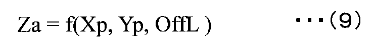
ここで、S65における半田29の高さの計算方法について、具体的に説明する。この場合、S63において、抽出した半田領域には、計測点Pが含まれているものとし、計測点Pにおける半田29の高さの計算方法について説明する。図21は、図20と同様に計測点Pにおけるz−x断面図である。図20と同様に、x軸が紙面の左右方向(主走査方向)を示し、z軸が高さ方向を示し、y軸は紙面の表裏方向(副走査方向)となる。そして、計測点Pと撮像部12とを通る線l上において、配線パターンの近似面SRとの交点をAとし、ランドの近似面SLとの交点をBとし、高さ0点、すなわちx軸との交点をCとする。そして、点A、点P、点B、および点Cのx位置およびy位置を座標(Xp、Yp)とする。
Here, the method for calculating the height of the
まず、ACの長さを算出する。ここで、点Aは、配線パターンの近似面SR上の点であるため、(x、y)に(Xp、Yp)を代入して、ACの長さは、以下の式より算出される。 First, the length of AC is calculated. Here, since the point A is a point on the approximate plane SR of the wiring pattern, (Xp, Yp) is substituted for (x, y), and the length of AC is calculated by the following equation.
![]()
![]()
このとき、ZaがACの長さとなる。 At this time, Za is the length of AC.
また、PCの長さを算出する。すなわち、計測点Pの高さを計測する。計測点Pは、半田29上の点であって、この半田29はランド35c上に塗布されるものである。したがって、計測点Pの高さは、半田29を含むランド35cの高さである。ここで、CPU44は、半田ランド高さ計測手段として作動する。
Also, the length of the PC is calculated. That is, the height of the measurement point P is measured. The measurement point P is a point on the
そして、配線パターンの近似面SR上の点Aにおける接線Laとx軸とでなす角度θを算出する。図22は、図21の半田29およびランド35cの部分を拡大した図であって、接線Laと角度θとを示す図である。ここで、接線Laは、座標(Xp、Yp)における接線であるため、接線Laの傾き(tanθ)は、配線パターンの近似面SRの式を偏微分し、(x、y)に(Xp、Yp)を代入することにより得ることができる。なお、ランドの近似面SL上の点Bにおける接線Lbとx軸とでなす角度も同じθであり、ランドの近似面SLの式を偏微分しても同じ結果となる。偏微分した結果を以下に示す。
Then, an angle θ formed by the tangent line La and the x axis at the point A on the approximate surface SR of the wiring pattern is calculated. FIG. 22 is an enlarged view of the portion of the
この式に、(x、y)に(Xp、Yp)を代入すると以下のようになり、角度θを算出することができる。 Substituting (Xp, Yp) for (x, y) in this equation results in the following, and the angle θ can be calculated.
また、計測点Pを通り、接線La、Lbに平行な直線をLpとし、点Aを通り、La、Lb、Lpに垂直な直線をLtとし、LpとLtとの交点をMとし、LbとLtとの交点をNとする。図23は、交点M、Nを示す図である。 A straight line passing through the measurement point P and parallel to the tangent lines La and Lb is set as Lp, a straight line passing through the point A and perpendicular to La, Lb and Lp is set as Lt, an intersection of Lp and Lt is set as M, and Lb and Let N be the intersection with Lt. FIG. 23 is a diagram showing the intersection points M and N. FIG.
そして、半田29の高さをDとすると、D=AN−AMで算出する。すなわち、この場合、半田29の高さDを計測するための基準は、オフセットから算出されるランドの高さとなる。ここで、ANの長さは、S64で読み出したOffLの値であり、AMの長さは、APcosθであり、APの長さは、AC−PCで算出することができる。その結果、Dは、以下の式で算出されることとなる。
If the height of the
なお、このようなS62〜S65の処理は、複数の検査ブロック毎に繰り返し実施される。 Note that such processing of S62 to S65 is repeatedly performed for each of a plurality of inspection blocks.
このように、この発明に係る三次元形状計測装置10は、所定の領域、ここでは、配線パターンの高さに基づいて、所定の領域における高さ分布を算出し、この算出した高さ分布とランドの高さとの距離(オフセット)を算出する。この場合、所定の領域における高さ分布は、例えば基板25に反りや撓みが発生した場合であっても、その反りや撓みによる変化を含めたものとなる。その結果、算出した距離は、基板25の歪みによる影響を抑えたものなる。そして、半田29の高さを算出する際には、例えば基板25に半田29を塗布した後、基板25に歪みが発生した場合であっても、このような歪みの影響を抑えた距離を用いることができるため、正確に半田29の高さを算出することができる。
As described above, the three-dimensional
また、この場合、オフセットは、配線パターンとランドとの両方を考慮して算出された値であるため、従来のように配線パターンのみから算出されることなく、正確に半田29の高さを算出することができる。
In this case, since the offset is a value calculated in consideration of both the wiring pattern and the land, the height of the
また、この場合、半田塗布前の基板25においてオフセットを算出し、半田塗布後の基板25において、再度配線パターンにおける基板25の近似面を算出して、半田29の高さを計測する。したがって、半田塗布前の基板25の状態と半田塗布後の基板25の状態とが変化していた場合であっても、正確に半田29の高さを算出することができる。
In this case, the offset is calculated in the
また、この場合、半田29のみを高さを算出することができ、工業規格等に定められた定量的な半田量を検査に採用することができ、検査を適切に行うことができる。
Further, in this case, the height of only the
また、基板25の反りや撓みは、一般的に基板25毎に異なるものである。しかしながら、この場合、基板25毎にオフセットを算出して、半田29の高さを算出することができ、基板25毎に正確に半田29の高さを算出することができる。
Further, the warpage and deflection of the
なお、上記の実施の形態においては、2次曲面の例について説明したが、これに限ることなく、平面や他の形状の面にも適用することができる。この場合、(1)で示したS22における配線パターンの近似面Sr、および(2)で示したS23におけるランドの近似面Slは、以下の式で示すことができる。 In the above-described embodiment, an example of a quadratic curved surface has been described. However, the present invention is not limited to this, and the present invention can be applied to a flat surface or a surface having another shape. In this case, the approximate surface Sr of the wiring pattern in S22 shown in (1) and the approximate surface S1 of the land in S23 shown in (2) can be expressed by the following equations.
![]()
![]()
そして、ACの長さを算出する際の(x、y)に(Xp、Yp)を入力すると、以下の式で示すことができる。 When (Xp, Yp) is input to (x, y) when calculating the length of AC, it can be expressed by the following equation.
![]()
![]()
そして、(5)および(6)で示した配線パターンの近似面SR上の点Aにおける接線Laとx軸とでなす角度θを算出する際の式は、以下の式で示すことができる。 The equation for calculating the angle θ formed by the tangent line La and the x axis at the point A on the approximate surface SR of the wiring pattern shown in (5) and (6) can be expressed by the following equation.
なお、上記の実施の形態においては、所定の領域として、配線パターンを採用する例について説明したが、これに限ることなく、例えば、ランドの近傍のレジストの領域であってもよいし、他の領域であってよい。 In the above-described embodiment, the example in which the wiring pattern is adopted as the predetermined area has been described. However, the present invention is not limited to this, and may be, for example, a resist area in the vicinity of the land. It may be an area.
また、上記の実施の形態においては、撮像部12により撮像した画像を取得して、配線パターンの高さやランドの高さを計測することにより、オフセットを算出し、この算出したオフセットを用いて、半田の高さを算出する例について説明したが、これに限ることなく、例えば、予めオフセットの値をユーザにより設定されることにより、この設定されたオフセットを用いて、半田の高さを算出することとしてもよい。
In the above-described embodiment, an image captured by the
以上、図面を参照してこの発明の実施形態を説明したが、この発明は、図示した実施形態のものに限定されない。図示された実施形態に対して、この発明と同一の範囲内において、あるいは均等の範囲内において、種々の修正や変形を加えることが可能である。 As mentioned above, although embodiment of this invention was described with reference to drawings, this invention is not limited to the thing of embodiment shown in figure. Various modifications and variations can be made to the illustrated embodiment within the same range or equivalent range as the present invention.
この発明は、半田の高さの計測が必要となる場合に、有効に利用される。 The present invention is effectively used when it is necessary to measure the height of the solder.
10 三次元形状計測装置、11 投光部、12 撮像部、13 画像解析・駆動制御部、14 搬送部、15 計測対象、16 光パタン照射領域、17 光パタン非照射領域、22 光源、24 投光レンズ、25,49a,49b 基板、25a 面、26 パタン生成素子、27 光線分離部、29 半田、30 ランド、31 配線パターン、32 スルーホール、33 シルク、34 レジスト、35 検査ブロック、35a 配線パターンの領域、35b オフセット算出用の領域、35c ランドの領域、40 ラインセンサ、41 撮像レンズ、42 コントローラ、43 キャプチャボード、44 CPU、45 RAM、46 搬送ステージ、47 サーボモータ、48 基板掴持部、48a 基準面、50 設計情報取得機能、51 画像取得機能、52 画像拡張判定機能、53 配線パターン抽出機能、54 ランド抽出機能、55 半田抽出機能、56 近似面算出機能、57 高さ計測機能、58 ランドオフセット算出機能、59 ランドオフセット減算機能、60 検査機能、61 ランドオフセット記録機能、62 ランドオフセット読み込み機能。
DESCRIPTION OF
Claims (5)
基板は、半田が塗布される領域であるランドと、前記ランドの周囲を取り囲むように前記基板の上面に配置される所定の領域とを含み、
前記三次元形状計測装置は、
光パタンが投影された基板上の部材を撮像し、画像として取得する撮像手段と、
半田が塗布される前の状態の基板における、所定の基準面を基準とした前記所定の領域における高さ分布と前記ランドの高さ分布との距離を、ランドオフセットとして記憶する記憶手段と、
前記記憶手段に記憶された前記ランドオフセットを用いて、基板のランド上に塗布された半田の、当該ランドからの高さを計測する半田高さ計測手段とを備え、
前記半田高さ計測手段は、
半田を塗布された後の状態の基板において、前記所定の領域の画像を前記撮像手段により取得して、前記所定の基準面からの前記所定の領域の高さを計測し、計測した前記所定の領域の高さに基づいて、前記所定の領域における高さ分布を算出する塗布後領域高さ分布算出手段と、
半田を塗布された後の状態の基板において、前記ランド上に塗布された半田の画像を前記撮像手段により取得して、前記所定の基準面からの、半田を含むランドの高さを計測する塗布後ランド高さ計測手段と、
前記塗布後領域高さ分布算出手段により算出された前記所定の領域における高さ分布と、前記塗布後ランド高さ計測手段により計測された半田を含むランドの高さと、前記記憶手段に記憶された前記ランドオフセットとを用いて、半田の高さを算出する半田高さ算出手段とを含む、三次元形状計測装置。 A three-dimensional shape measuring apparatus for measuring a three-dimensional shape of a member on a substrate by analyzing an optical pattern projected on the member on the substrate,
The board includes a land that is an area where solder is applied, and a predetermined area that is disposed on the upper surface of the board so as to surround the land.
The three-dimensional shape measuring apparatus is
An imaging unit that captures an image of a member on the substrate on which the optical pattern is projected, and acquires the image as an image;
In the substrate in a state before the solder is applied, with reference to a predetermined reference plane the height distribution of the predetermined area the distance between the height distribution of the land, and storage means for storing as a land offset,
Solder height measuring means for measuring the height of the solder applied on the land of the substrate from the land using the land offset stored in the storage means;
The solder height measuring means includes
In the substrate in a state after the solder is applied, an image of the predetermined area is acquired by the imaging unit, the height of the predetermined area from the predetermined reference plane is measured, and the measured predetermined area is measured. A post-application region height distribution calculating means for calculating a height distribution in the predetermined region based on the height of the region;
Application in which the image of the solder applied on the land is acquired by the imaging means on the substrate in a state after the solder is applied, and the height of the land including the solder from the predetermined reference plane is measured. Rear land height measuring means,
The height distribution in the predetermined area calculated by the post-application area height distribution calculation means, the height of lands including solder measured by the post-application land height measurement means, and stored in the storage means A three-dimensional shape measuring apparatus comprising: a solder height calculating means for calculating a solder height using the land offset.
半田が塗布される前の状態の基板において、前記ランドの画像を取得して、前記所定の基準面からの前記ランドの高さを計測し、計測した前記ランドの高さと前記塗布前領域高さ分布算出手段により算出された前記所定の領域における高さ分布とに基づいて、前記ランドの高さ分布を算出する塗布前ランド高さ分布算出手段と、
前記塗布前領域高さ分布算出手段により算出された前記所定の領域における高さ分布と、前記塗布前ランド高さ分布算出手段により算出された前記ランドの高さ分布との距離を算出する距離算出手段とをさらに備え、
前記記憶手段は、前記距離算出手段により算出された距離を、前記ランドオフセットとして記憶する、請求項1に記載の三次元形状計測装置。 In the substrate in a state before the solder is applied, an image of the predetermined area is acquired, the height of the predetermined area from the predetermined reference plane is measured, and the height of the measured predetermined area is measured. A pre-application area height distribution calculating means for calculating a height distribution in the predetermined area,
In the substrate before the solder is applied, an image of the land is obtained, the height of the land from the predetermined reference surface is measured, and the measured height of the land and the height of the pre-application area Pre-application land height distribution calculating means for calculating the height distribution of the lands based on the height distribution in the predetermined area calculated by the distribution calculating means;
Distance calculation for calculating a height distribution in the predetermined region calculated by the pre-application region height distribution calculating means, the distance between the height distribution of the land calculated by the pre-application land height distribution calculating means And further comprising means,
The three-dimensional shape measurement apparatus according to claim 1, wherein the storage unit stores the distance calculated by the distance calculation unit as the land offset.
前記ランドの高さ分布とは、前記所定の基準面からの前記ランドの高さを、前記所定の領域における近似曲面と平行な近似曲面で表したものである、請求項1または2に記載の三次元形状計測装置。 Wherein a height distribution in a predetermined area state, and are a representation of the height from the predetermined reference plane in the predetermined area in the curved surface approximation,
The height distribution of the land is expressed by an approximate curved surface parallel to an approximate curved surface in the predetermined region, the height of the land from the predetermined reference plane . Three-dimensional shape measuring device.
基板は、半田が塗布される領域であるランドと、前記ランドの周囲を取り囲むように前記基板の上面に配置される所定の領域とを含むものであり、
半田が塗布される前の状態の基板において、所定の基準面を基準とした前記所定の領域における高さ分布と前記ランドの高さ分布との距離を、ランドオフセットとして記憶するステップと、
記憶された前記ランドオフセットを用いて、基板のランド上に塗布された半田の、当該ランドからの高さを計測する計測ステップとを備え、
前記計測ステップは、
半田を塗布された後の状態の基板において、前記所定の基準面からの前記所定の領域の高さを計測し、計測した前記所定の領域の高さに基づいて、前記所定の領域における高さ分布を算出するステップと、
半田を塗布された後の状態の基板において、前記所定の基準面からの、半田を含むランドの高さを計測するステップと、
算出された前記所定の領域における高さ分布と、計測された半田を含むランドの高さと、記憶された前記ランドオフセットとを用いて、半田の高さを算出するステップとを含む、三次元形状計測方法。 A three-dimensional shape measuring method for measuring a three-dimensional shape of a member on a substrate,
The substrate includes a land to which solder is applied and a predetermined region disposed on the upper surface of the substrate so as to surround the periphery of the land.
In the substrate in a state before the solder is applied, and storing the distance between the height distribution of the predetermined area relative to the predetermined reference plane and the height distribution of the land, as land offset,
A measurement step of measuring the height of the solder applied on the land of the substrate from the land using the stored land offset;
The measurement step includes
In the substrate after the solder is applied, the height of the predetermined area from the predetermined reference plane is measured, and the height in the predetermined area is determined based on the measured height of the predetermined area. Calculating a distribution;
In the substrate in a state after the solder is applied, measuring the height of the land including the solder from the predetermined reference surface;
A step of calculating the height of the solder using the calculated height distribution in the predetermined region, the height of the land including the measured solder, and the stored land offset; Measurement method.
Priority Applications (4)
| Application Number | Priority Date | Filing Date | Title |
|---|---|---|---|
| JP2011040511A JP5772062B2 (en) | 2011-02-25 | 2011-02-25 | Three-dimensional shape measuring apparatus and three-dimensional shape measuring method |
| KR1020110102792A KR20120098386A (en) | 2011-02-25 | 2011-10-10 | Three-dimensional shape measuring device and three-dimensional shape measuring method |
| US13/280,566 US20120218562A1 (en) | 2011-02-25 | 2011-10-25 | Three-dimensional shape measurement apparatus and three-dimensional shape measurement method |
| EP11186829.5A EP2492633B1 (en) | 2011-02-25 | 2011-10-27 | Three-dimensional shape measurement apparatus and three-dimensional shape measurement method |
Applications Claiming Priority (1)
| Application Number | Priority Date | Filing Date | Title |
|---|---|---|---|
| JP2011040511A JP5772062B2 (en) | 2011-02-25 | 2011-02-25 | Three-dimensional shape measuring apparatus and three-dimensional shape measuring method |
Publications (2)
| Publication Number | Publication Date |
|---|---|
| JP2012177611A JP2012177611A (en) | 2012-09-13 |
| JP5772062B2 true JP5772062B2 (en) | 2015-09-02 |
Family
ID=45524239
Family Applications (1)
| Application Number | Title | Priority Date | Filing Date |
|---|---|---|---|
| JP2011040511A Active JP5772062B2 (en) | 2011-02-25 | 2011-02-25 | Three-dimensional shape measuring apparatus and three-dimensional shape measuring method |
Country Status (4)
| Country | Link |
|---|---|
| US (1) | US20120218562A1 (en) |
| EP (1) | EP2492633B1 (en) |
| JP (1) | JP5772062B2 (en) |
| KR (1) | KR20120098386A (en) |
Families Citing this family (3)
| Publication number | Priority date | Publication date | Assignee | Title |
|---|---|---|---|---|
| KR101614061B1 (en) * | 2012-03-29 | 2016-04-20 | 주식회사 고영테크놀러지 | Apparatus for joint inspection |
| US20140293011A1 (en) * | 2013-03-28 | 2014-10-02 | Phasica, LLC | Scanner System for Determining the Three Dimensional Shape of an Object and Method for Using |
| DE102015121673B4 (en) * | 2015-12-11 | 2019-01-10 | SmartRay GmbH | shape investigation |
Family Cites Families (17)
| Publication number | Priority date | Publication date | Assignee | Title |
|---|---|---|---|---|
| US4876455A (en) * | 1988-02-25 | 1989-10-24 | Westinghouse Electric Corp. | Fiber optic solder joint inspection system |
| US5028799A (en) * | 1988-08-01 | 1991-07-02 | Robotic Vision System, Inc. | Method and apparatus for three dimensional object surface determination using co-planar data from multiple sensors |
| JP3314406B2 (en) * | 1992-04-24 | 2002-08-12 | 松下電器産業株式会社 | How to measure the height of cream solder |
| US5465152A (en) * | 1994-06-03 | 1995-11-07 | Robotic Vision Systems, Inc. | Method for coplanarity inspection of package or substrate warpage for ball grid arrays, column arrays, and similar structures |
| US5995232A (en) * | 1997-07-14 | 1999-11-30 | U.S. Philips Corporation | Method of and device for inspecting a PCB |
| US6750899B1 (en) * | 2000-01-07 | 2004-06-15 | Cyberoptics Corporation | Solder paste inspection system |
| US6496270B1 (en) * | 2000-02-17 | 2002-12-17 | Gsi Lumonics, Inc. | Method and system for automatically generating reference height data for use in a three-dimensional inspection system |
| JP2002098513A (en) * | 2000-09-22 | 2002-04-05 | Tani Denki Kogyo Kk | Lens frame form measuring device |
| JP3850282B2 (en) * | 2001-12-12 | 2006-11-29 | 松下電器産業株式会社 | Pattern surface automatic extraction method and shape measuring apparatus using the same |
| JP2004292409A (en) * | 2003-03-28 | 2004-10-21 | Sumitomo Chem Co Ltd | Method for producing chlorosilane compound |
| JP3868917B2 (en) * | 2003-03-31 | 2007-01-17 | シーケーディ株式会社 | Three-dimensional measuring device and inspection device |
| JP4746841B2 (en) * | 2004-01-23 | 2011-08-10 | ルネサスエレクトロニクス株式会社 | Manufacturing method of semiconductor integrated circuit device |
| JP4613644B2 (en) * | 2005-03-09 | 2011-01-19 | パナソニック株式会社 | Circuit board inspection method |
| JP4735010B2 (en) * | 2005-04-06 | 2011-07-27 | パナソニック株式会社 | Substrate height measurement method |
| US7545512B2 (en) * | 2006-01-26 | 2009-06-09 | Koh Young Technology Inc. | Method for automated measurement of three-dimensional shape of circuit boards |
| JP4992811B2 (en) * | 2008-04-18 | 2012-08-08 | パナソニック株式会社 | Electronic component mounting equipment |
| JP4892602B2 (en) * | 2009-10-30 | 2012-03-07 | ルネサスエレクトロニクス株式会社 | Manufacturing method of semiconductor integrated circuit device |
-
2011
- 2011-02-25 JP JP2011040511A patent/JP5772062B2/en active Active
- 2011-10-10 KR KR1020110102792A patent/KR20120098386A/en active IP Right Grant
- 2011-10-25 US US13/280,566 patent/US20120218562A1/en not_active Abandoned
- 2011-10-27 EP EP11186829.5A patent/EP2492633B1/en active Active
Also Published As
| Publication number | Publication date |
|---|---|
| US20120218562A1 (en) | 2012-08-30 |
| KR20120098386A (en) | 2012-09-05 |
| EP2492633B1 (en) | 2019-03-06 |
| EP2492633A1 (en) | 2012-08-29 |
| JP2012177611A (en) | 2012-09-13 |
Similar Documents
| Publication | Publication Date | Title |
|---|---|---|
| JP6151406B2 (en) | Board inspection method | |
| JP2009198440A (en) | Correction pattern image generation device, pattern inspection apparatus, and correction pattern image generation method | |
| JP5307876B2 (en) | Inspection method | |
| KR20010040998A (en) | Automatic inspection system with stereovision | |
| KR101237497B1 (en) | Method of setting inspection area | |
| KR20150003783A (en) | X-ray inspection method and x-ray inspection device | |
| KR101729862B1 (en) | Data correcting apparatus, drawing apparatus, inspection apparatus, data correcting method, drawing method, inspection method and recording medium | |
| US20150045927A1 (en) | Stencil programming and inspection using solder paste inspection system | |
| JP5772062B2 (en) | Three-dimensional shape measuring apparatus and three-dimensional shape measuring method | |
| KR101121992B1 (en) | Method of Forming Mounting Inspection Data, Media Storing the Same, and Inspection Apparatus using the Same | |
| JP2019100753A (en) | Printed circuit board inspection device and printed circuit board inspection method | |
| JP2007033040A (en) | Method and device for calibrating optical head part in three-dimensional shape measuring instrument by optical cutting method | |
| JP6781963B1 (en) | Measuring device and measuring method | |
| JP2019219357A (en) | Imaging apparatus, imaging method, and imaging program | |
| TWI612296B (en) | Data correcting apparatus, drawing apparatus, inspection apparatus, data correcting method, drawing method, inspection method and recording medium carrying program | |
| KR101863439B1 (en) | Data correcting apparatus, drawing apparatus, inspection apparatus, data correcting method, drawing method, inspection method and program recorded on recording medium | |
| JP4772815B2 (en) | Correction pattern image generation apparatus, pattern inspection apparatus, and correction pattern image generation method | |
| JP4034325B2 (en) | Three-dimensional measuring device and inspection device | |
| JP2011047857A (en) | Method of measuring three-dimensional shape | |
| CN104991420A (en) | Drawing apparatus, substrate processing system and drawing method | |
| JP3868917B2 (en) | Three-dimensional measuring device and inspection device | |
| JP2009058311A (en) | Marking inspection device | |
| JP2007072232A (en) | Reference image forming apparatus, pattern inspection apparatus, reference image forming method, and reticle | |
| JP6903243B2 (en) | Measuring device and measuring method | |
| JP6868935B1 (en) | Measuring device and measuring method |
Legal Events
| Date | Code | Title | Description |
|---|---|---|---|
| RD03 | Notification of appointment of power of attorney |
Free format text: JAPANESE INTERMEDIATE CODE: A7423 Effective date: 20130130 |
|
| A621 | Written request for application examination |
Free format text: JAPANESE INTERMEDIATE CODE: A621 Effective date: 20130919 |
|
| A977 | Report on retrieval |
Free format text: JAPANESE INTERMEDIATE CODE: A971007 Effective date: 20140228 |
|
| A131 | Notification of reasons for refusal |
Free format text: JAPANESE INTERMEDIATE CODE: A131 Effective date: 20140304 |
|
| A521 | Request for written amendment filed |
Free format text: JAPANESE INTERMEDIATE CODE: A523 Effective date: 20140428 |
|
| A131 | Notification of reasons for refusal |
Free format text: JAPANESE INTERMEDIATE CODE: A131 Effective date: 20141014 |
|
| A521 | Request for written amendment filed |
Free format text: JAPANESE INTERMEDIATE CODE: A523 Effective date: 20141208 |
|
| TRDD | Decision of grant or rejection written | ||
| A01 | Written decision to grant a patent or to grant a registration (utility model) |
Free format text: JAPANESE INTERMEDIATE CODE: A01 Effective date: 20150602 |
|
| A61 | First payment of annual fees (during grant procedure) |
Free format text: JAPANESE INTERMEDIATE CODE: A61 Effective date: 20150615 |
|
| R150 | Certificate of patent or registration of utility model |
Ref document number: 5772062 Country of ref document: JP Free format text: JAPANESE INTERMEDIATE CODE: R150 |
|
| R250 | Receipt of annual fees |
Free format text: JAPANESE INTERMEDIATE CODE: R250 |
|
| R250 | Receipt of annual fees |
Free format text: JAPANESE INTERMEDIATE CODE: R250 |