JP5771187B2 - Substrate processing technology - Google Patents
Substrate processing technology Download PDFInfo
- Publication number
- JP5771187B2 JP5771187B2 JP2012504863A JP2012504863A JP5771187B2 JP 5771187 B2 JP5771187 B2 JP 5771187B2 JP 2012504863 A JP2012504863 A JP 2012504863A JP 2012504863 A JP2012504863 A JP 2012504863A JP 5771187 B2 JP5771187 B2 JP 5771187B2
- Authority
- JP
- Japan
- Prior art keywords
- ion beam
- mask
- substrate
- height
- ion
- Prior art date
- Legal status (The legal status is an assumption and is not a legal conclusion. Google has not performed a legal analysis and makes no representation as to the accuracy of the status listed.)
- Expired - Fee Related
Links
- 239000000758 substrate Substances 0.000 title claims description 149
- 238000012545 processing Methods 0.000 title description 24
- 238000010884 ion-beam technique Methods 0.000 claims description 196
- 238000000034 method Methods 0.000 claims description 93
- 150000002500 ions Chemical class 0.000 claims description 66
- 238000005468 ion implantation Methods 0.000 claims description 45
- 238000004519 manufacturing process Methods 0.000 claims description 9
- 238000003672 processing method Methods 0.000 claims description 6
- 239000002019 doping agent Substances 0.000 description 46
- 125000006850 spacer group Chemical group 0.000 description 15
- 239000000463 material Substances 0.000 description 14
- 239000007789 gas Substances 0.000 description 10
- 230000008569 process Effects 0.000 description 10
- XUIMIQQOPSSXEZ-UHFFFAOYSA-N Silicon Chemical compound [Si] XUIMIQQOPSSXEZ-UHFFFAOYSA-N 0.000 description 9
- 238000002513 implantation Methods 0.000 description 9
- 229910052710 silicon Inorganic materials 0.000 description 8
- 239000010703 silicon Substances 0.000 description 8
- 230000001133 acceleration Effects 0.000 description 6
- 238000009792 diffusion process Methods 0.000 description 6
- 239000012535 impurity Substances 0.000 description 6
- 229910052796 boron Inorganic materials 0.000 description 4
- 238000002347 injection Methods 0.000 description 4
- 239000007924 injection Substances 0.000 description 4
- -1 boron ions Chemical class 0.000 description 3
- 229910052751 metal Inorganic materials 0.000 description 3
- 239000002184 metal Substances 0.000 description 3
- 238000012986 modification Methods 0.000 description 3
- 230000004048 modification Effects 0.000 description 3
- MARUHZGHZWCEQU-UHFFFAOYSA-N 5-phenyl-2h-tetrazole Chemical compound C1=CC=CC=C1C1=NNN=N1 MARUHZGHZWCEQU-UHFFFAOYSA-N 0.000 description 2
- IJGRMHOSHXDMSA-UHFFFAOYSA-N Atomic nitrogen Chemical compound N#N IJGRMHOSHXDMSA-UHFFFAOYSA-N 0.000 description 2
- KTSFMFGEAAANTF-UHFFFAOYSA-N [Cu].[Se].[Se].[In] Chemical compound [Cu].[Se].[Se].[In] KTSFMFGEAAANTF-UHFFFAOYSA-N 0.000 description 2
- 238000001816 cooling Methods 0.000 description 2
- 238000012937 correction Methods 0.000 description 2
- 238000013461 design Methods 0.000 description 2
- 230000000694 effects Effects 0.000 description 2
- 238000000605 extraction Methods 0.000 description 2
- 239000011521 glass Substances 0.000 description 2
- 230000003287 optical effect Effects 0.000 description 2
- 229920002120 photoresistant polymer Polymers 0.000 description 2
- 238000013519 translation Methods 0.000 description 2
- ZOXJGFHDIHLPTG-UHFFFAOYSA-N Boron Chemical compound [B] ZOXJGFHDIHLPTG-UHFFFAOYSA-N 0.000 description 1
- OKTJSMMVPCPJKN-UHFFFAOYSA-N Carbon Chemical compound [C] OKTJSMMVPCPJKN-UHFFFAOYSA-N 0.000 description 1
- GYHNNYVSQQEPJS-UHFFFAOYSA-N Gallium Chemical compound [Ga] GYHNNYVSQQEPJS-UHFFFAOYSA-N 0.000 description 1
- UFHFLCQGNIYNRP-UHFFFAOYSA-N Hydrogen Chemical compound [H][H] UFHFLCQGNIYNRP-UHFFFAOYSA-N 0.000 description 1
- OAICVXFJPJFONN-UHFFFAOYSA-N Phosphorus Chemical compound [P] OAICVXFJPJFONN-UHFFFAOYSA-N 0.000 description 1
- 229910052787 antimony Inorganic materials 0.000 description 1
- WATWJIUSRGPENY-UHFFFAOYSA-N antimony atom Chemical compound [Sb] WATWJIUSRGPENY-UHFFFAOYSA-N 0.000 description 1
- 229910052785 arsenic Inorganic materials 0.000 description 1
- RQNWIZPPADIBDY-UHFFFAOYSA-N arsenic atom Chemical compound [As] RQNWIZPPADIBDY-UHFFFAOYSA-N 0.000 description 1
- QVGXLLKOCUKJST-UHFFFAOYSA-N atomic oxygen Chemical compound [O] QVGXLLKOCUKJST-UHFFFAOYSA-N 0.000 description 1
- 230000015572 biosynthetic process Effects 0.000 description 1
- 230000008859 change Effects 0.000 description 1
- 150000001875 compounds Chemical class 0.000 description 1
- 239000000356 contaminant Substances 0.000 description 1
- 239000013078 crystal Substances 0.000 description 1
- 238000010586 diagram Methods 0.000 description 1
- 229910052733 gallium Inorganic materials 0.000 description 1
- 229910002804 graphite Inorganic materials 0.000 description 1
- 239000010439 graphite Substances 0.000 description 1
- 238000010438 heat treatment Methods 0.000 description 1
- 239000001307 helium Substances 0.000 description 1
- 229910052734 helium Inorganic materials 0.000 description 1
- SWQJXJOGLNCZEY-UHFFFAOYSA-N helium atom Chemical compound [He] SWQJXJOGLNCZEY-UHFFFAOYSA-N 0.000 description 1
- 239000001257 hydrogen Substances 0.000 description 1
- 229910052739 hydrogen Inorganic materials 0.000 description 1
- 238000007654 immersion Methods 0.000 description 1
- 239000007943 implant Substances 0.000 description 1
- 229910052738 indium Inorganic materials 0.000 description 1
- APFVFJFRJDLVQX-UHFFFAOYSA-N indium atom Chemical compound [In] APFVFJFRJDLVQX-UHFFFAOYSA-N 0.000 description 1
- 238000001802 infusion Methods 0.000 description 1
- 238000005259 measurement Methods 0.000 description 1
- 229910052757 nitrogen Inorganic materials 0.000 description 1
- 239000001301 oxygen Substances 0.000 description 1
- 229910052760 oxygen Inorganic materials 0.000 description 1
- 238000004806 packaging method and process Methods 0.000 description 1
- 229910052698 phosphorus Inorganic materials 0.000 description 1
- 239000011574 phosphorus Substances 0.000 description 1
- 239000010453 quartz Substances 0.000 description 1
- 230000009467 reduction Effects 0.000 description 1
- 230000000630 rising effect Effects 0.000 description 1
- 229910052594 sapphire Inorganic materials 0.000 description 1
- 239000010980 sapphire Substances 0.000 description 1
- 239000004065 semiconductor Substances 0.000 description 1
- VYPSYNLAJGMNEJ-UHFFFAOYSA-N silicon dioxide Inorganic materials O=[Si]=O VYPSYNLAJGMNEJ-UHFFFAOYSA-N 0.000 description 1
- 230000001629 suppression Effects 0.000 description 1
- 238000011144 upstream manufacturing Methods 0.000 description 1
Images


Classifications
-
- H—ELECTRICITY
- H01—ELECTRIC ELEMENTS
- H01L—SEMICONDUCTOR DEVICES NOT COVERED BY CLASS H10
- H01L31/00—Semiconductor devices sensitive to infrared radiation, light, electromagnetic radiation of shorter wavelength or corpuscular radiation and specially adapted either for the conversion of the energy of such radiation into electrical energy or for the control of electrical energy by such radiation; Processes or apparatus specially adapted for the manufacture or treatment thereof or of parts thereof; Details thereof
- H01L31/04—Semiconductor devices sensitive to infrared radiation, light, electromagnetic radiation of shorter wavelength or corpuscular radiation and specially adapted either for the conversion of the energy of such radiation into electrical energy or for the control of electrical energy by such radiation; Processes or apparatus specially adapted for the manufacture or treatment thereof or of parts thereof; Details thereof adapted as photovoltaic [PV] conversion devices
- H01L31/06—Semiconductor devices sensitive to infrared radiation, light, electromagnetic radiation of shorter wavelength or corpuscular radiation and specially adapted either for the conversion of the energy of such radiation into electrical energy or for the control of electrical energy by such radiation; Processes or apparatus specially adapted for the manufacture or treatment thereof or of parts thereof; Details thereof adapted as photovoltaic [PV] conversion devices characterised by at least one potential-jump barrier or surface barrier
- H01L31/068—Semiconductor devices sensitive to infrared radiation, light, electromagnetic radiation of shorter wavelength or corpuscular radiation and specially adapted either for the conversion of the energy of such radiation into electrical energy or for the control of electrical energy by such radiation; Processes or apparatus specially adapted for the manufacture or treatment thereof or of parts thereof; Details thereof adapted as photovoltaic [PV] conversion devices characterised by at least one potential-jump barrier or surface barrier the potential barriers being only of the PN homojunction type, e.g. bulk silicon PN homojunction solar cells or thin film polycrystalline silicon PN homojunction solar cells
-
- H—ELECTRICITY
- H01—ELECTRIC ELEMENTS
- H01L—SEMICONDUCTOR DEVICES NOT COVERED BY CLASS H10
- H01L21/00—Processes or apparatus adapted for the manufacture or treatment of semiconductor or solid state devices or of parts thereof
- H01L21/02—Manufacture or treatment of semiconductor devices or of parts thereof
- H01L21/04—Manufacture or treatment of semiconductor devices or of parts thereof the devices having at least one potential-jump barrier or surface barrier, e.g. PN junction, depletion layer or carrier concentration layer
- H01L21/18—Manufacture or treatment of semiconductor devices or of parts thereof the devices having at least one potential-jump barrier or surface barrier, e.g. PN junction, depletion layer or carrier concentration layer the devices having semiconductor bodies comprising elements of Group IV of the Periodic System or AIIIBV compounds with or without impurities, e.g. doping materials
- H01L21/26—Bombardment with radiation
- H01L21/263—Bombardment with radiation with high-energy radiation
- H01L21/265—Bombardment with radiation with high-energy radiation producing ion implantation
- H01L21/266—Bombardment with radiation with high-energy radiation producing ion implantation using masks
-
- H—ELECTRICITY
- H01—ELECTRIC ELEMENTS
- H01L—SEMICONDUCTOR DEVICES NOT COVERED BY CLASS H10
- H01L31/00—Semiconductor devices sensitive to infrared radiation, light, electromagnetic radiation of shorter wavelength or corpuscular radiation and specially adapted either for the conversion of the energy of such radiation into electrical energy or for the control of electrical energy by such radiation; Processes or apparatus specially adapted for the manufacture or treatment thereof or of parts thereof; Details thereof
- H01L31/18—Processes or apparatus specially adapted for the manufacture or treatment of these devices or of parts thereof
- H01L31/1804—Processes or apparatus specially adapted for the manufacture or treatment of these devices or of parts thereof comprising only elements of Group IV of the Periodic System
-
- H—ELECTRICITY
- H01—ELECTRIC ELEMENTS
- H01J—ELECTRIC DISCHARGE TUBES OR DISCHARGE LAMPS
- H01J2237/00—Discharge tubes exposing object to beam, e.g. for analysis treatment, etching, imaging
- H01J2237/30—Electron or ion beam tubes for processing objects
- H01J2237/317—Processing objects on a microscale
- H01J2237/31701—Ion implantation
- H01J2237/31706—Ion implantation characterised by the area treated
- H01J2237/3171—Ion implantation characterised by the area treated patterned
- H01J2237/31711—Ion implantation characterised by the area treated patterned using mask
-
- Y—GENERAL TAGGING OF NEW TECHNOLOGICAL DEVELOPMENTS; GENERAL TAGGING OF CROSS-SECTIONAL TECHNOLOGIES SPANNING OVER SEVERAL SECTIONS OF THE IPC; TECHNICAL SUBJECTS COVERED BY FORMER USPC CROSS-REFERENCE ART COLLECTIONS [XRACs] AND DIGESTS
- Y02—TECHNOLOGIES OR APPLICATIONS FOR MITIGATION OR ADAPTATION AGAINST CLIMATE CHANGE
- Y02E—REDUCTION OF GREENHOUSE GAS [GHG] EMISSIONS, RELATED TO ENERGY GENERATION, TRANSMISSION OR DISTRIBUTION
- Y02E10/00—Energy generation through renewable energy sources
- Y02E10/50—Photovoltaic [PV] energy
- Y02E10/547—Monocrystalline silicon PV cells
-
- Y—GENERAL TAGGING OF NEW TECHNOLOGICAL DEVELOPMENTS; GENERAL TAGGING OF CROSS-SECTIONAL TECHNOLOGIES SPANNING OVER SEVERAL SECTIONS OF THE IPC; TECHNICAL SUBJECTS COVERED BY FORMER USPC CROSS-REFERENCE ART COLLECTIONS [XRACs] AND DIGESTS
- Y02—TECHNOLOGIES OR APPLICATIONS FOR MITIGATION OR ADAPTATION AGAINST CLIMATE CHANGE
- Y02P—CLIMATE CHANGE MITIGATION TECHNOLOGIES IN THE PRODUCTION OR PROCESSING OF GOODS
- Y02P70/00—Climate change mitigation technologies in the production process for final industrial or consumer products
- Y02P70/50—Manufacturing or production processes characterised by the final manufactured product
Description
本発明は、基板を処理するための技術に関連し、特に、ドーパント又は不純物を基板に導入するための技術に関連する。 The present invention relates to techniques for processing a substrate, and more particularly to techniques for introducing dopants or impurities into a substrate.
電子デバイスの製造においては、基板の元々の機械的性質、光学的性質、又は電気的性質を変化させるために、ドーパント又は不純物を基板に導入する。メモリデバイスの製造においては、ホウ素イオンをケイ素基板に導入することがある。結晶格子内のケイ素原子とホウ素イオンとが異なる電気的性質を有することから、十分な量のホウ素イオンを導入することによって、ケイ素基板の電気的性質を変化させることができる。 In the manufacture of electronic devices, dopants or impurities are introduced into the substrate to change the original mechanical, optical, or electrical properties of the substrate. In the manufacture of memory devices, boron ions may be introduced into the silicon substrate. Since silicon atoms and boron ions in the crystal lattice have different electrical properties, the electrical properties of the silicon substrate can be changed by introducing a sufficient amount of boron ions.
ドーパントを導入するためには、イオン注入技術を用いることができる。この技術では、所望の種を含む供給材料をイオン化する。その後、供給材料のイオンを、所望エネルギーを有するイオンビームの形態で、基板に向けて指向させ、その後注入する。イオンが互いに異なる種からなる場合、イオンによって基板の性質を変化させることができる。 In order to introduce the dopant, an ion implantation technique can be used. In this technique, a feed material containing the desired species is ionized. The feed ions are then directed towards the substrate in the form of an ion beam having the desired energy and then implanted. When ions are made of different species, the properties of the substrate can be changed by the ions.
他のケイ素基板ベースのデバイスである太陽電池も、イオン又はドーパントをケイ素基板に導入することにより製造することができる。従来では、ドーパントを含むガラス又はペーストをケイ素基板上に設けて行う拡散処理により、ドーパントを導入していた。その後、基板を加熱し、ガラス又はペースト内のドーパントを熱拡散により基板内に拡散させる。 Other silicon substrate-based devices, solar cells, can also be fabricated by introducing ions or dopants into the silicon substrate. Conventionally, the dopant is introduced by a diffusion treatment performed by providing glass or paste containing the dopant on the silicon substrate. Thereafter, the substrate is heated, and the dopant in the glass or paste is diffused into the substrate by thermal diffusion.
拡散処理は、コスト効果が高いものであり得るが、多くの欠点を有する。一部の太陽電池では、選択的ドーピングを行って基板の選択領域のみにドーパントを導入することが望ましい。しかしながら、拡散処理は制御が困難であり、拡散による選択的ドーピングを達成することは困難であり得る。当該処理は、不精密なドーピング又は不均一なドープ領域の形成をもたらし得る。さらに、拡散処理中に、空隙、空気泡、又は他の汚染物質が、ドーパントと共に基板に導入され得る。 Diffusion treatment can be cost effective, but has many drawbacks. In some solar cells, it is desirable to perform selective doping to introduce dopants only into selected regions of the substrate. However, the diffusion process is difficult to control and it can be difficult to achieve selective doping by diffusion. The treatment can result in inaccurate doping or formation of non-uniform doped regions. Furthermore, voids, air bubbles, or other contaminants can be introduced into the substrate along with the dopant during the diffusion process.
かかる欠点に対処するために、イオン注入処理によるドーピングが提案されてきた。提案された処理では、基板をフォトレジスト層で覆い、リソグラフィック処理を行って基板の一部分を露出させる。その後、イオン注入を行い、ドーパントを露出部分に注入する。この処理は、精密な選択的ドーピングを達成するが、安価ではない。フォトレジストで覆い、パターンを形成し、フォトレジストを除去するためのさらなるステップ及び時間が必要となり、その各々により製造処理のコストが増大される。露出させるべき領域が極度に小さい場合、これらのステップはさらに複雑となり得る。 In order to deal with such drawbacks, doping by ion implantation has been proposed. In the proposed process, the substrate is covered with a photoresist layer and a lithographic process is performed to expose a portion of the substrate. Thereafter, ion implantation is performed, and a dopant is implanted into the exposed portion. This process achieves precise selective doping, but is not cheap. Additional steps and time are required to cover, pattern, and remove the photoresist, each of which increases the cost of the manufacturing process. These steps can be further complicated if the area to be exposed is extremely small.
太陽電池の製造に追加されるコストにより、太陽電池により低コストのエネルギーを生産しにくくなる。一方、高効率・高性能の太陽電池の製造におけるコストの低減は、世界中で太陽電池の実装に良い影響を与えるはずである。これにより、クリーンエネルギー技術のより幅広い利用及び採用が可能になる。 The cost added to the manufacture of solar cells makes it difficult to produce low cost energy with solar cells. On the other hand, cost reductions in the production of highly efficient and high performance solar cells should have a positive impact on solar cell packaging worldwide. This allows for wider use and adoption of clean energy technology.
したがって、新規技術が要求されている。 Therefore, new technology is required.
本発明は、基板を処理するための改良技術を開示するものである。1つの特定の例示的実施形態において、本技術は、基板の処理方法として実現することができる。当該方法は、複数のイオンを含むイオンビームを、イオンビーム経路に沿ってイオン源から基板に向けて指向させるステップと、マスクの少なくとも一部分を、イオンビーム経路内でイオン源と基板との間に設けるステップと、基板及びマスクのうち一方を、基板及びマスクのうち他方に対して平行移動させるステップと、を含むことができる。 The present invention discloses an improved technique for processing a substrate. In one particular exemplary embodiment, the technology may be implemented as a substrate processing method. The method includes directing an ion beam including a plurality of ions from an ion source toward a substrate along an ion beam path, and at least a portion of a mask between the ion source and the substrate in the ion beam path. Providing and translating one of the substrate and mask relative to the other of the substrate and mask.
この特定の例示的実施形態の他の態様によれば、マスクを、イオンビームに対して固定配置することができる。 According to another aspect of this particular exemplary embodiment, the mask can be fixedly positioned with respect to the ion beam.
この特定の例示的実施形態の他の態様によれば、マスクは、互いに離間した複数のフィンガーを備え、少なくとも1つのギャップを規定することができる。 According to another aspect of this particular exemplary embodiment, the mask can comprise a plurality of fingers spaced apart from each other to define at least one gap.
この特定の例示的実施形態の他の態様によれば、マスクは、複数のフィンガーを支持するベースを備えることができる。 According to another aspect of this particular exemplary embodiment, the mask can comprise a base that supports a plurality of fingers.
この特定の例示的実施形態の他の態様によれば、上記マスクの少なくとも一部分を、イオンビームの高さ方向に延在させることができるとともに、イオンビームの第1部の経路内に設けることができる。 According to another aspect of this particular exemplary embodiment, at least a portion of the mask can extend in the height direction of the ion beam and be provided in the path of the first portion of the ion beam. it can.
この特定の例示的実施形態の他の態様によれば、イオンビームは、第2部をさらに備えることができ、 マスクの少なくとも一部分を、イオンビームの第2部の経路内に設けないようにする。 According to another aspect of this particular exemplary embodiment, the ion beam can further comprise a second portion such that at least a portion of the mask is not provided in the path of the second portion of the ion beam. .
この特定の例示的実施形態の他の態様によれば、イオンビームの第1部の高さを、イオンビームの第2部の高さにほぼ等しくすることができる。 According to another aspect of this particular exemplary embodiment, the height of the first portion of the ion beam can be approximately equal to the height of the second portion of the ion beam.
この特定の例示的実施形態の他の態様によれば、イオンビームの第1部の高さを、イオンビームの第2部の高さよりも大きくすることができる。 According to another aspect of this particular exemplary embodiment, the height of the first portion of the ion beam can be greater than the height of the second portion of the ion beam.
この特定の例示的実施形態の他の態様によれば、イオンビームの第1部の高さとイオンビームの第2部の高さとの比を、約3:2とすることができる。 According to another aspect of this particular exemplary embodiment, the ratio of the height of the first part of the ion beam to the height of the second part of the ion beam can be about 3: 2.
この特定の例示的実施形態の他の態様によれば、イオンビームの第1部の高さを、イオンビームの第2部の高さより小さくすることができる。 According to another aspect of this particular exemplary embodiment, the height of the first portion of the ion beam can be less than the height of the second portion of the ion beam.
この特定の例示的実施形態の他の態様によれば、イオンビームの第1部の高さとイオンビームの第2部の高さとの比を、約2:3とすることができる。 According to another aspect of this particular exemplary embodiment, the ratio of the height of the first part of the ion beam to the height of the second part of the ion beam can be about 2: 3.
この特定の例示的実施形態の他の態様によれば、マスクは、互いに離間した複数のフィンガーを備え、少なくとも1つのギャップを規定することができ、イオンビームの第1部からのイオンの一部を、マスクの少なくとも1つのギャップを通過させ、基板に注入して、選択的イオン注入を行うことができる。 According to another aspect of this particular exemplary embodiment, the mask comprises a plurality of fingers spaced apart from each other, can define at least one gap, and a portion of ions from the first part of the ion beam Can be passed through at least one gap of the mask and implanted into the substrate for selective ion implantation.
この特定の例示的実施形態の他の態様によれば、イオンビームの第2部からのイオンを、基板に注入して、ブランケットイオン注入を行うことができる。 According to another aspect of this particular exemplary embodiment, ions from the second part of the ion beam can be implanted into the substrate for blanket ion implantation.
この他の例示的実施形態によれば、本技術は、基板の処理方法として実現することができる。上記方法は、イオンビームをイオン源から基板に向けてイオンビーム経路に沿って指向させるステップであって、イオンビームは複数のイオンを含む、ステップと、イオン源と基板との間でイオンビーム経路内にマスクを設けるステップであって、マスクの少なくとも一部分を、イオンビームの全体高さの一部のみに亘ってイオンビームの高さ方向に延在させている、ステップと、を含むことができる。 According to other exemplary embodiments, the present technology can be implemented as a substrate processing method. The method includes directing an ion beam along an ion beam path from an ion source toward a substrate, the ion beam including a plurality of ions, and the ion beam path between the ion source and the substrate. Providing a mask therein, wherein at least a portion of the mask extends in the height direction of the ion beam over only a portion of the total height of the ion beam. .
この特定の例示的実施形態の他の態様によれば、マスク及びイオンビームを、相対的に固定配置することができる。 According to another aspect of this particular exemplary embodiment, the mask and ion beam can be relatively fixedly positioned.
この特定の例示的実施形態の他の態様によれば、上記方法は、マスク及び基板のうち少なくともいずれか一方を、マスク及び基板のうち他方に対して、平行移動させるステップをさらに含むことができる。 According to another aspect of this particular exemplary embodiment, the method can further include translating at least one of the mask and the substrate relative to the other of the mask and the substrate. .
この特定の例示的実施形態の他の態様によれば、イオンビームは、第1部及び第2部を有することができ、マスクの少なくとも一部分を、イオンビームの第1部の経路内に設け、マスクの少なくとも一部分を、イオンビームの第2部の経路内に設けないようにしている。 According to another aspect of this particular exemplary embodiment, the ion beam can have a first part and a second part, wherein at least a portion of the mask is provided in the path of the first part of the ion beam; At least a part of the mask is not provided in the path of the second part of the ion beam.
この特定の例示的実施形態の他の態様によれば、イオンビームの第1部の高さを、イオンビームの第2部の高さにほぼ等しくすることができる。 According to another aspect of this particular exemplary embodiment, the height of the first portion of the ion beam can be approximately equal to the height of the second portion of the ion beam.
この特定の例示的実施形態の他の態様によれば、イオンビームの第1部の高さを、イオンビームの第2部の高さより大きくすることができる。 According to another aspect of this particular exemplary embodiment, the height of the first portion of the ion beam can be greater than the height of the second portion of the ion beam.
この特定の例示的実施形態の他の態様によれば、イオンビームの第1部の高さとイオンビームの第2部の高さとの比を、約3:2とすることができる。 According to another aspect of this particular exemplary embodiment, the ratio of the height of the first part of the ion beam to the height of the second part of the ion beam can be about 3: 2.
この特定の例示的実施形態の他の態様によれば、イオンビームの第1部の高さを、イオンビームの第2部の高さより小さくする。 According to another aspect of this particular exemplary embodiment, the height of the first part of the ion beam is less than the height of the second part of the ion beam.
この特定の例示的実施形態の他の態様によれば、イオンビームの第1部の高さとイオンビームの第2部の高さとの比を、約2:3とすることができる。 According to another aspect of this particular exemplary embodiment, the ratio of the height of the first part of the ion beam to the height of the second part of the ion beam can be about 2: 3.
この特定の例示的実施形態の他の態様によれば、マスクは、互いに離間した複数のフィンガーを備え、1つ以上のギャップを規定することができ、イオンビームの第1部からのイオンの一部を、フィンガーにより規定した1つ以上のギャップを通過させることができる。 According to another aspect of this particular exemplary embodiment, the mask comprises a plurality of fingers spaced apart from each other, can define one or more gaps, and one of the ions from the first part of the ion beam. The part can be passed through one or more gaps defined by the fingers.
この特定の例示的実施形態の他の態様によれば、上記方法は、イオンビームの第1部からのイオンを用いて選択的イオン注入を行い、イオンビームの第2部からのイオンを用いてブランケットイオン注入を行うステップとを、さらに含むことができる。 According to another aspect of this particular exemplary embodiment, the method performs selective ion implantation using ions from the first part of the ion beam and using ions from the second part of the ion beam. Performing blanket ion implantation.
他の特定の例示的実施形態によれば、本技術は、基板の処理方法として実現することができる。上記方法は、複数のイオンを含むイオンビームを、イオンビーム経路に沿って指向させるステップと、イオンビームの第1部からのイオンを用いて基板に対してブランケットイオン注入を行い、イオンビームの第2部からのイオンを用いて基板に対して選択的イオン注入を行うステップであって、第1部及び第2部をイオンビームの互いに対向する側に配置している、実行ステップとを、含むことができる。 According to other specific exemplary embodiments, the present technology can be implemented as a substrate processing method. The method includes directing an ion beam including a plurality of ions along an ion beam path, performing blanket ion implantation on the substrate using ions from the first part of the ion beam, and Performing selective ion implantation on the substrate using ions from two parts, wherein the first part and the second part are arranged on opposite sides of the ion beam. be able to.
この特定の例示的実施形態の他の態様によれば、上記実行ステップは、イオンビームの第2部の経路内にマスクの少なくとも一部分を設けずに、イオンビームの第1部の経路内にマスクの当該少なくとも一部分を設けることを含むことができる。 According to another aspect of this particular exemplary embodiment, the performing step includes providing a mask in the path of the first part of the ion beam without providing at least a portion of the mask in the path of the second part of the ion beam. Providing at least a portion thereof.
この特定の例示的実施形態の他の態様によれば、選択的イオン注入を、イオンビームの第1部の幅方向に設けられた1つ以上のギャップを通過するイオンを用いて行うことができる。 According to another aspect of this particular exemplary embodiment, selective ion implantation can be performed using ions that pass through one or more gaps provided in the width direction of the first portion of the ion beam. .
この特定の例示的実施形態の他の態様によれば、上記方法は、イオンビーム及びマスクを固定配置するステップと、マスク及び基板のうち一方を、マスク及び基板のうち他方に対して平行移動させるステップとを、さらに含むことができる。 According to another aspect of this particular exemplary embodiment, the method includes: placing the ion beam and mask fixed; and translating one of the mask and substrate relative to the other of the mask and substrate. A step can be further included.
以下、本発明について、図面に示す例示的実施形態を参照しつつ、さらに詳細に説明する。以下では、本発明について、例示的実施形態を参照しつつ説明するが、本発明がこれに限定されないことは明らかである。当業者は、本明細書で説明する本発明の範囲内に属する他の実装、変更、実施形態、及び使用分野であって、本発明が大いに有用となり得るものを、理解するはずである。 Hereinafter, the present invention will be described in more detail with reference to exemplary embodiments shown in the drawings. In the following, the present invention will be described with reference to exemplary embodiments, but it is clear that the present invention is not limited thereto. Those skilled in the art will appreciate other implementations, modifications, embodiments, and fields of use that are within the scope of the invention described herein, and that the invention can be greatly useful.
ここで、基板を処理するための技術の実施形態を幾つか説明する。明確かつ単純な説明のために、実施形態の説明は、基板にドーパント又は不純物を導入する技術を中心とする場合がある。例えば、本明細書で説明する技術は、異なるドーズ量又は準位の不純物を含む領域及び/又は異なる型の不純物又はドーパントを含む領域を形成するために用いることができる。本発明は、特定の技術を中心に説明するが、これに限られるものではない。 Several embodiments of techniques for processing a substrate will now be described. For clarity and simplicity, the description of the embodiments may focus on techniques for introducing dopants or impurities into the substrate. For example, the techniques described herein can be used to form regions containing different doses or levels of impurities and / or regions containing different types of impurities or dopants. The present invention will be described focusing on a specific technique, but is not limited thereto.
本開示では、リボンビームを用いたビームラインイオン注入システムに関する実施形態を説明する。スポットイオンビーム又は集束イオンビームを用いた走査ビームイオン注入システムを含む、他の種類のイオン注入システムについては、詳細に説明しないが、除外されるものではない。さらに、例えば、プラズマ支援ドーピング(PLAD: Plasma Assisted Doping)システム又はプラズマ浸漬イオン注入(PIII: Plasma Immersion Ion Implantation)システムを含む、他の種類の基板処理システムを、同等に使用することができる。 In this disclosure, embodiments relating to a beamline ion implantation system using a ribbon beam are described. Other types of ion implantation systems, including scanning beam ion implantation systems using spot or focused ion beams, are not described in detail but are not excluded. In addition, other types of substrate processing systems can be used equally, including, for example, a Plasma Assisted Doping (PLAD) system or a Plasma Immersion Ion Implantation (PIII) system.
実施形態で開示する基板は、太陽電池を製造するためのケイ素ベースの基板とすることができる。ケイ素ベースの基板について主に説明するが、本発明は、他の材料を含む基板に、同等に使用することができる。例えば、テルル化カドミウム(CdTe)、セレン化銅インジウムガリウム(CIGS)、又は他の材料を含む基板も、使用することができる。さらに、他の非太陽電池の基板も、本発明に使用することができる。他の機械デバイス、電子デバイス(例えばメモリデバイス)、又は光学デバイス(例えば発光ダイオード)、又は他のデバイスの製造に、金属基板、他の半導体基板、及び絶縁基板を、同等に使用することができる。 The substrate disclosed in the embodiments can be a silicon-based substrate for manufacturing solar cells. Although primarily silicon based substrates will be described, the present invention can be used equally well with substrates containing other materials. For example, substrates comprising cadmium telluride (CdTe), copper indium gallium selenide (CIGS), or other materials can also be used. Furthermore, other non-solar cell substrates can also be used in the present invention. Metal substrates, other semiconductor substrates, and insulating substrates can be used equally well in the manufacture of other mechanical devices, electronic devices (eg, memory devices), or optical devices (eg, light emitting diodes), or other devices. .
図1は、本発明の技術を用いて製造した例示的な基板100を示す。本実施形態では、太陽電池基板100を示している。基板100は、一方側において、1つ以上のコンタクト領域102を含むことができる。各コンタクト領域102上には、金属コンタクト部(図示せず)を形成することができる。コンタクト領域102は、領域102内に所望のドーパントを所定ドーズ量だけ導入することにより、形成することができる。基板100が2つ以上のコンタクト領域102を含む場合、スペーサー領域104によりコンタクト領域102を互いに離間させることができる。一部の実施形態において、基板100は、1つ以上のスペーサー領域104を備えることもでき、各スペーサー領域104にドーパント又は不純物を導入することもできる。本実施形態では、コンタクト領域102とスペーサー領域104に導入するドーパント種を、互いに同一とすることができる。ただし、コンタクト領域102のドーパントのドーズ量は、スペーサー領域104のドーパントのドーズ量よりも、多くすることができる。基板が太陽電池である場合、基板100の正面上において高濃度にドープしたコンタクト領域102と低濃度にドープしたスペーサー領域104とを含むこのパターンを、選択的エミッタ設計と称する場合がある。高濃度にドープしたコンタクト領域102により、コンタクト領域102と金属コンタクト部との間のインタフェースを向上することができる。さらに、ドーパントのドーズ量をより多くすることにより、コンタクト領域102の導電率をより高くすることができる。他の実施形態において、コンタクト領域102とスペーサー領域104とに、異なるドーパント種を導入することができるが、好ましくはない。例えば、コンタクト領域102及びスペーサー領域104のうち一方にp型ドーパントを導入し、コンタクト領域102及びスペーサー領域104のうち他方にn型ドーパントを導入することができる。他の例では、コンタクト領域102及びスペーサー領域104に、同じ型で異なる種のドーパントを導入することができる。さらに、コンタクト領域102内のドーパントのドーズ量を、スペーサー領域104内のドーパントのドーズ量よりも多くすることもできる。代案として、コンタクト領域102内のドーパントのドーズ量を、スペーサー領域104内のドーパントのドーズ量以下とすることができる。
FIG. 1 illustrates an
図2は、本発明の一実施形態による基板を処理するための例示的システム200を示す。本実施形態において、システム200は、図1に示す選択的エミッタ設計を有する太陽電池基板を製造するために使用することができる。図2に示すように、システム200は、イオン形態のドーパントを基板100に導入し得るビームラインイオン注入システムとすることができる。
FIG. 2 illustrates an
本実施形態のイオン注入システム200は、所望のドーパント種の供給ガスを含むガスボックス230に接続されたイオン源202を含むことができる。ガスボックス230からの供給ガスは、イオン源202に供給され、その後イオン化される。この供給ガスは、I族及び3A〜8A族に属する1以上の元素のドーパント種を含むことができる。例えば、供給ガスは、水素(H)、ヘリウム(He)、他の希ガス、酸素(O)、窒素(N)、ヒ素(As)、ホウ素(B)、リン(P)、アンチモン、ガリウム(Ga)、インジウム(In)、又は他のガスを含むことができる。さらに、供給ガスは、カルボランC2B10H12又は他の分子化合物を含むことができる。供給ガスがイオン化された後、イオン源202内のイオン20は、抑制電極201a及び接地電極201bを含む引き出し電極201により引き出される。電源(図示せず)は、引き出し電極201に接続することができ、可変電圧を供給することができる。
The
イオン注入システム200は、随意的なビームラインコンポーネントを備えることもできる。他の実施形態におけるシステムでビームラインコンポーネントを省略することができるため、ビームラインコンポーネントは、随意とすることができる。ビームラインコンポーネントを含む場合、随意的なビームラインコンポーネントは、質量分析器203、角度補正磁石207、第1加速/減速ステージ205、及び第2加速/減速ステージ209のうち少なくともいずれか1つを含むことができる。
The
質量分析器203は、イオンの質量に応じてイオンを偏向させることができる。所望の質量を有するイオンを、十分に偏向させ、質量分析器203の出口側アパーチャを通過させ、システム200のさらに下流を移動させることができる。一方、不所望の質量を有するイオンを、不十分に又は過剰に偏向させ、質量分析器203の壁に向けて指向させることができる。一方、角度補正磁石207は、発散経路内を移動するイオン20を、ほぼ平行な経路内を移動するようにコリメートすることができる。本実施形態では、発散するイオンビーム20を、ほぼ平行なリボン型のイオンビーム20へとコリメートすることができる。第1加速/減速ステージ205及び第2加速/減速ステージ207を含む場合、第1加速/減速ステージ205及び第2加速/減速ステージ207は、イオンビーム経路に沿って移動するイオンビーム20内のビームを、加速又は減速させることができる。
The
イオンビーム経路に沿って移動するイオンビーム20は、エンドステーション206に向けて指向させことができる。エンドステーション206内には、基板100内にイオンビーム20内のイオンを注入し得るように、1つ以上の基板100を、イオンビーム経路内に配置することができる。注入処理を制御するために、エンドステーション206は、様々なコンポーネントを含むことができる。例えば、エンドステーション206は、1つ以上の基板100を支持し得るプラテン214を含むことができる。プラテン214は、基板100を支持することに加えて、例えば基板100の温度を制御して、高温イオン注入又は低温イオン注入をもたらすこともできる。低温イオン注入をもたらすために、プラテン214は、基板100を室温より低い温度、好ましくは273°K未満の温度に、維持することができる。高温イオン注入をもたらすために、プラテン214は、基板100を室温より高い温度、好ましくは293°Kより高い温度に、維持することができる。プラテン214に加えて、本発明のイオン注入システム200は、イオン注入前又はイオン注入後に基板100を冷却又は加熱し得る、冷却及び/又は加熱ステーション(図示せず)を含むことができる。
The
エンドステーション206は、基板100をイオンビーム20の経路内に配置し得るスキャナー(図示せず)、例えばロプラット(roplat)を含むこともできる。スキャナーは、基板100をイオンビーム20に対して所望の位置及び配向まで平行移動/回転させることもできる。一実施形態では、イオンがほぼ0°の入射角又は注入角で注入されるように、基板100を、イオンビーム経路に対してほぼ垂直に配向させることができる。他の実施形態では、非ゼロの入射角又は注入角をもたらすように、基板を、イオンビーム20に対して非垂直にすることができる。一実施形態では、注入処理全体を通じて、注入角を一定に維持することができる。他の実施形態では、注入処理中に、注入角を変化させることができる。本発明では、注入されるイオンのドーズ量を制御するために、基板を所望速度で平行移動させることもできる。適切なドーズ量を保証するために、エンドステーション306は、ドーズ量測定システムを含むこともできる。
The
イオン源202と基板100との間には、1つ以上のマスク250を配置することができる。本発明において、マスク250は、イオン20が基板100に到達するのを阻止するために、1つ以上のフィンガーを含むことができる。マスク250は、イオン20を通過させて基板100に注入し得るような、1つ以上のアパーチャを含むこともできる。マスク250は、エンドステーション206の壁を含むシステム200の様々なコンポーネントにより、支持することができる。マスク250を支持する様々なコンポーネントによって、イオンビーム20及び/又は基板100に対するマスク250の適切な配向又は位置をもたらすことができる。例えば、アクチュエータ(図示せず)をマスク250に接続して、マスク250を基板100及び/又はイオンビーム20に対して平行移動させ、回転させ、又は傾けることができる。マスク250の温度が過度に上昇するのを防ぐために、マスク250の冷却手段を設けることもできる。
One or
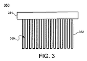
図3は、本発明の一実施形態による例示的なマスク350を示す。本実施の形態において、マスク350は、少なくとも1つのフィンガー352を備えることができる。マスク350は、随意にベース354を含むことができ、フィンガー352をベース354により支持することができる。マスク350がベース354を含まない場合、マスク350は、共に支持及び/又は保持される1つ以上のフィンガー352とすることができる。マスク350が2つ以上のフィンガー352を備える場合、フィンガー352を互いに離間させて、ギャップ又はアパーチャ356を規定することができる。一実施形態において、マスク350は、複数のフィンガー352を有して1つ以上のギャップ又はアパーチャを規定することができ、フィンガー352は、互いに均一の形状又は寸法を有することができる。さらに、ギャップ又はアパーチャ356が均一の形状又は寸法を有するように、フィンガー352を構成することができる。他の実施形態において、マスク350は、61個のフィンガー352を有することができ、フィンガー352は、60個の均一かつ矩形状のアパーチャ356を形成するように構成される。ただし、マスク350が任意数のフィンガー352及びアパーチャ356を有し得ることは、当業者に理解されるはずである。さらに、アパーチャ356は、均一又は非均一に関わらず、様々な形状及び寸法を有することができる。
FIG. 3 illustrates an
マスク350は、様々な材料で作ることができる。マスクは、イオン注入の反応条件に耐え得る不活性材料で作ることが好ましい。マスク350に含まれる材料の例は、石英、グラファイト、サファイア、ケイ素(Si)、SiC、及びSiNを含むことができる。他の材料の例を、マスク350に含めることもできる。他の材料の例は、ドーパント種を含む材料を含むことができる。
The
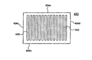
図4は、本発明の他の実施形態による他の例示的なマスク450を示す。本実施形態において、マスク450は、少なくとも1つのフィンガー452を備えることができる。マスク450は、フィンガー452を支持し、マスク450の互いに対向する側に設けられた、第1ベース454a及び第2ベース454bを備えることもできる。必要に応じて、マスク450は、マスク450の互いに対向する側において、フィンガーの隣に設けられた第3ベース454c及び第4ベース454dを含むこともできる。代案として、第3ベース454c及び第4ベース454dを、追加のフィンガー452に置き換えることができる。マスク450が2つ以上のフィンガー452を備える場合、フィンガー452を互いに離間させて、1つ以上のギャップ又はアパーチャ456を規定することができる。一実施形態において、マスク450は、複数のフィンガー452を有することができ、フィンガー452は、均一の形状及び寸法を有することができる。さらに、アパーチャ450が均一の形状及び寸法を有するように、フィンガー452を構成することができる。ただし、マスク456が任意数のフィンガー452及びアパーチャ456を有し得ることは、当業者に理解されるはずである。さらに、アパーチャ456は、均一又は非均一に関わらず、様々な形状及び寸法を有することができる。
FIG. 4 illustrates another
図3に示した上記実施形態のマスク350と同様に、マスク450は、様々な材料を含むことができる。明確かつ単純な説明のために、材料の説明を省略する。
Similar to the
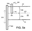
図5a及び図5bは、本発明の一実施形態による基板を処理するための例示的な技術を示す。これらの図は、必ずしも原寸に比例して描かれていない。明確かつ単純な説明のために、図2に示すビームラインイオン注入システム200及び図3に示すマスク350を参照して、この技術を説明する。ただし、スポットイオンビーム又は集束イオンビームを用いた走査ビームイオン注入システムを含む、他のシステムを使用することもできる。さらに、図4に示すマスク450を含む、他のマスクを使用することもできる。明確かつ単純な説明のために、本技術をビーム高さに関して説明する場合がある。リボンビームイオン注入装置について、ビーム高さが、リボンビームの実際の高さを意味し得ることは、当業者に理解されるはずである。スポットビーム又は集束ビームを用いる走査ビームイオン注入装置に対して、この用語は、リボンビームイオン注入装置の効果と同様の効果を達成するようにスポットビームにより走査される領域の高さを意味し得る。
Figures 5a and 5b illustrate an exemplary technique for processing a substrate according to one embodiment of the invention. These figures are not necessarily drawn to scale. For clarity and simplicity, the technique will be described with reference to the beamline
本実施形態では、基板500及びマスク350を、イオン注入システム200内に設けることができる。図5a及び図5bに示すように、マスク350のフィンガー352を、矢印510に示す高さ方向に基板500の全体高さに亘って延びないように、寸法決め又は配置することができる。フィンガー352を、イオンビーム20の全体高さに亘って延びないように、寸法決め又は配置することもできる。本実施形態において、マスク350のフィンガー352は、イオンビーム20の高さの約50%に亘って延びることができる。フィンガー352が全体高さの一部のみに亘って延びることにより、基板500に向けて指向されたときのイオンビーム20を、複数の部分に分割することができる。例えば、イオンビーム20は、イオンビーム20の第1エッジ20iから仮想基準線20iiiまで延びる第1部20aを備えることができる。イオンビーム20は、イオンビーム20の第2エッジ20iiから基準線20iiiまで延びる第2部20bを備えることもできる。基準線20iiiは、フィンガーの一端352iにより規定することができる。
In this embodiment, the
フィンガー352がイオンビーム20の高さの約50%に亘って延びる場合、イオンビーム20の第1部20a及び第2部20bの高さを、ほぼ等しくすることができる。イオンビームの第1部20aのイオンを、基板500に直接注入して、ブランケット(blanket)イオン注入を行うことができる。一方、第2部20bのイオンの一部を、アパーチャ356を介して基板500に注入して、選択的イオン注入を行うことができる。
When the
イオンビーム20、マスク350、及び基板500の各々は、個別の回転自由度及び平行移動自由度を有することができる。イオンビーム20、マスク350、及び基板500は、連帯して又は個別に、傾け、回転させ、及び/又は平行移動させることができる。本実施形態では、マスク350を、イオンビーム20に対して固定配置することができる。一方、基板500は、矢印510で示す高さ方向に、イオンビーム20及び/又はマスク350に対して平行移動させることができる。詳細には説明しないが、他の実施形態では、基板500を、矢印512で示す方向に、イオンビーム20及び/又はマスク350に対して平行移動させることもできる。基板500が高さ方向510に平行移動するとき、ドーパントを含む第1領域502及び第2領域504を形成することができる。第1領域502は、イオンビームの第1部20a及び第2部20bからのドーパントが注入されることから、高濃度ドープ領域とすることができる。一方、第2領域504は、イオンビームの第1部20aからのドーパント又はイオンが注入されることから、低濃度ドープ領域とすることができる。本実施形態の基板500を図1に示す基板100と比較すると、高濃度にドープした第1領域502はコンタクト領域102に対応し、低濃度にドープした第2領域504はスペーサー領域104に対応し得る。コンタクト領域102のドーパントのドーズ量がスペーサー領域104のドーパントのドーズ量よりも少ない他の実施形態において、高濃度にドープした第1領域502はスペーサー領域104に対応し、低濃度にドープした第2領域504はコンタクト領域102に対応し得る。
Each of the
フィンガー352及びイオンビーム20の高さに応じて、第1領域502及び第2領域504内のドーパントのドーズ量及び準位を調節することができる。本実施形態において、フィンガー352の高さは、イオンビーム20の高さの約50%とすることができる。その結果、フィンガー352によりもたらされるイオンビームの第1部20a及び第2部20bは、等しい高さを有することができる。イオンビーム20内のイオン量は、高さ方向510にほぼ均一であり、かつ基板500の平行移動速度が一定である場合は、第1領域502内のドーパントのドーズ量を、第2領域504内のドーパントのドーズ量の約2倍とすることができる。例えば、第1領域502内のドーパントのドーズ量を約2E15/cm2とすることができ、第2領域504内のドーパントのドーズ量を1E15/cm2とすることができる。他の実施形態では、フィンガー352の高さを、イオンビーム20の高さの約33%(3分の1)とすることができる。この実施形態では、イオンビームの第1部20aの高さを、第2部20bの高さより約50%大きくすることができる。イオン注入後、第1領域502内のドーパントの量を、第2領域504内のドーパントの量より約50%多くすることができる。これにより、第1領域502及び第2領域504内のドーパントのドーズ量の比を、約3:2とすることができる。
The dose amount and level of the dopant in the
ドーパントのドーズ量の制御に加えて、フィンガー352の高さを調節することで、イオンビームの均一性の調節をもたらすことができる。例えば、2xの均一な注入を達成するように、マスク350のフィンガー352の長さを調節することができる。
In addition to controlling the dose of the dopant, adjusting the height of the
本発明の技術を用いて、ドーパントのドーズ量が異なる2つの領域を有する基板を製造することができる。従来技術とは異なり、本発明の技術を使用すれば、1本のイオンビームを用いて、又はイオンビームを1回通過させて、ブランケット注入及び選択的注入を達成し、同時又はほぼ同時に、2つの領域を生成することができる。さらに、この技術は、2つの異なるマスクを必要としない。さらに、異なるマスクを設け、異なるマスクを用いて処理し、マスクを除去するという追加的なステップを回避することができる。本開示で説明した技術の方が、ずっと単純かつ効率的である。 Using the technique of the present invention, a substrate having two regions with different dopant doses can be manufactured. Unlike the prior art, the technique of the present invention can be used to achieve blanket implantation and selective implantation with a single ion beam or with a single pass of the ion beam, simultaneously or nearly simultaneously. One region can be generated. Furthermore, this technique does not require two different masks. Furthermore, the additional steps of providing different masks, processing with different masks and removing the masks can be avoided. The technique described in this disclosure is much simpler and more efficient.
図6は、本発明の一実施形態による基板を処理するための他の例示的な技術を示す。この図は、必ずしも原寸に比例して描かれていない。本実施形態が、上記実施形態で説明した特徴と同様の特徴を多く含むことは、当業者に理解されるはずである。明確かつ単純な説明のために、同様の特徴の説明を繰り返さない場合がある。これらの特徴は、必ずしも原寸に比例して描かれていない。 FIG. 6 illustrates another exemplary technique for processing a substrate according to one embodiment of the present invention. This figure is not necessarily drawn to scale. It should be understood by those skilled in the art that this embodiment includes many features similar to those described in the above embodiment. For clarity and simplicity, the description of similar features may not be repeated. These features are not necessarily drawn to scale.
本実施形態において、マスク650は、少なくとも1つのフィンガー652を備えることができ、複数のフィンガー652を互いに離間させて、ギャップ又はアパーチャ656を規定することができる。例えば、イオンビーム30は、イオンビーム30の第1エッジ30iから仮想基準線30iiiまで延びる第1部30aを備えることができる。イオンビーム30は、イオンビーム30の第2エッジ30iiから基準線30iiiまで延びる第2部30bを備えることもできる。基準線30iiiは、フィンガーの一端652iにより規定することができる。
本実施形態において、基板500及びマスク650を、イオン注入システム内に設けることができる。その後、イオンビーム30を基板500に向けて指向させることができる。本実施形態において、イオンビーム30に対する基板500の平行移動を不要とし得るように、矢印510で示す方向に沿ったイオンビーム30の高さを、十分に大きくすることができる。言い換えれば、注入されるべき基板500内の領域をイオンビーム30の高さにより包囲し得るとともに、基板500及びイオンビーム30の一方を他方に対して平行移動させる必要が無いほど、イオンビーム30の高さは、十分に大きい。
In this embodiment, the
In this embodiment, the
一方、本実施形態のマスク650は、マスク350と同様とすることができる。前述した実施形態と同様に、本実施形態のイオンビーム30、マスク650、及び基板500の各々は、個別の回転自由度及び平行移動自由度を有することができる。ただし、基板500及びイオンビーム30は、連帯して傾け、回転させ、及び/又は平行移動させ得るように、相対的に固定配置することができる。一方、マスク650は、イオンビーム30及び基板500に対して、平行移動させることができる。マスク650が高さ方向に平行移動するとき、高濃度にドープした第1領域502及び低濃度にドープした第2領域504を形成することができる。第1領域502及び第2領域504へのさらなるドーパントの注入を防ぐために、本実施形態のマスク650は、より大きな高さのベース654を随意に含むことができる。本実施形態の技術では、マスク650をイオンビーム30に対して平行移動させることにより、高濃度にドープした第1領域502及び低濃度にドープした第2領域504を得ることができる。
On the other hand, the
図7は、本発明の他の実施形態による他の例示的なマスク750を示す。本実施形態において、マスク750は、マスク750の互いに対向する側に設けられた上部702及び下部704を備えることができる。上部702及び下部704の各々が、図3に示した上記実施形態のマスク350と同様であることは、当業者に理解されるはずである。上部702及び下部704の各々において、マスク750は、1つ以上の第1フィンガー752a及び1つ以上の第2フィンガー752bを備えることができる。マスク750は、第1フィンガー752a及び第2フィンガー752bを支持する随意的な第1ベース754a及び第2ベース754bを備えることもできる。さらに、マスク750は、フィンガーの隣において互いに対向する側に設けられた随意的な第3ベース754c及び第4ベース754dを含むこともできる。
FIG. 7 illustrates another
マスク750の上部702及び下部704の各々が2つ以上の第1フィンガー752a及び第2フィンガー752bを備える場合、フィンガー752a、752bを幅方向712に互いに離間させ、1つ以上の第1アパーチャ756aを規定することができる。マスク750は、高さ方向710に互いに離間した上部702及び下部704により規定した第2アパーチャ756bを備えることもできる。
When each of the
上記実施形態のマスク350、450と同様に、本実施形態のマスク750は、様々な材料を含むことができる。
Similar to the
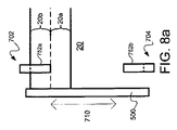
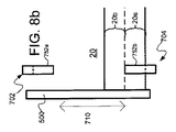
図8a及び図8bは、本発明の他の実施形態による基板を処理するための他の例示的な技術を示す。これらの図は、必ずしも原寸に比例して描かれていない。明確かつ単純な説明のために、本実施形態の技術を、図7に示すマスク750を参照して説明する。本技術を他のマスクを用いて使用し得ることは、当業者に理解されるはずである。さらに、説明を簡単かつ単純にするために、随意的な第3ベース754c及び第4ベース754dを図示していない。
Figures 8a and 8b illustrate another exemplary technique for processing a substrate according to another embodiment of the present invention. These figures are not necessarily drawn to scale. For the sake of clear and simple explanation, the technique of the present embodiment will be described with reference to a
本実施形態の技術は、複数部からなる技術とすることができ、第1部を図5a及び図5bを参照して説明した技術と同様とし得る。したがって、本実施形態の技術は、図5a及び図5bを参照して説明した上記実施形態の技術と共に理解されるべきである。 The technique of this embodiment can be a technique consisting of a plurality of parts, and the first part can be the same as the technique described with reference to FIGS. 5a and 5b. Therefore, the technique of the present embodiment should be understood together with the technique of the above-described embodiment described with reference to FIGS. 5a and 5b.
本実施形態において、マスク750を、イオン源(図示せず)と基板500との間に設けることができる。その後、イオンビーム20を、イオンビームの経路に沿って基板500に指向させることができる。本技術の第1部中では、イオンビーム20を、マスク750の上部702に指向させることができ、マスク750の上部702を、イオンビームの経路内に設けることができる。図8aに示すように、第1フィンガー752aがイオンビーム20の全体高さに亘って延びないように、第1フィンガー752aを寸法決め又は配置することができる。この処理では、イオンビーム20を、第1部20a及び第2部20bに分割することができる。イオンビーム20の第1部20a内のイオンを、第2アパーチャ756bを介して基板に直接注入して、ブランケットイオン注入を行うことができる。一方、イオンビーム20の第2部20bからのイオンの一部を、1つ以上の第1アパーチャ756aを通過させて、選択的イオン注入を行うことができる。図5a及び図5bに示した技術と同様に、基板500を高さ方向710に平行移動させることができる。ただし、マスク750の上部702は、イオンビーム20に対して固定配置することができる。結果として、高濃度ドープ領域(図示せず)及び低濃度ドープ領域(図示せず)を、基板500上に形成することができる。
In the present embodiment, the
第1部の後又は前に起こり得る本技術の第2部中では、イオンビーム20をマスク750の下部704に向けて指向させることができる。本技術の第1部と同様に、第2フィンガー752bがイオンビーム20の全体高さに亘って延びないように、第2フィンガー752bを寸法決め又は配置することができる。この処理では、イオンビーム20を、第1部20a及び第2部20bに分割することができる。本技術の第1部とは異なり、イオンビームの第1部20aを、マスク750の下部704内の第1アパーチャ756aを介して選択的イオン注入を行うために用いることができる。一方、ブランケットイオン注入を、イオンビーム20の第2部20bを用いて行うことができる。
In the second part of the present technology, which can occur after or before the first part, the
本実施形態の技術は、複数の利点をもたらす。本技術は、特に、高さ方向710におけるイオンビーム20の非均一性に対処するために用いることができる。多くのイオン注入装置では、非均一性、例えばイオンのドーズ量のバラツキが、高さ方向に存在することがある。このバラツキは、特に、空間電荷効果により発生し得る。イオンビームの第1部及び第2部の両方を用いて高濃度ドープ領域及び低濃度ドープ領域を生成することにより、非均一性を軽減することができる。
The technique of the present embodiment provides a plurality of advantages. The present technology can be used to address non-uniformity of the
さらに、基板に対するマスク750の位置を決定することができる。例えば、基板500及びイオンビーム20に対する第1フィンガー752a及び第2フィンガー752bの相対位置を補正することなく、マスク750を、基板500の上流に設けることができる。イオンビーム20をマスク750に指向させることができる。フィンガー752a、752bに起因するイオンビームの損失に応じて、「ウェハーマップ」を生成することができる。さらに、イオンビーム又は基板が高さ方向710に走査する速度を、いかなる反対称性をも補償するように、調節することができる。例えば、基板500がイオン注入されていないときに、基板500を方向転換させる間に、マスク750をイオンビームに対して移動させることができる。これにより、イオンビームの非均一性を、基板のブランケット注入された部分内で相殺することができる。基板を方向転換させる度にマスク750を移動させる必要はないが、イオンビームの変動とのオーバーラップを最小化させる間隔で移動させることができる。例えば、これにより、50Hz及び60Hzの高調波を回避することができる。
Furthermore, the position of the
図9は、本発明の他の実施形態による他の例示的なマスク950を示す。明確かつ単純な説明のために、マスク950について、アパーチャに関して説明する場合がある。マスク950は、高さ方向910に、アパーチャ956a〜956cの複数の行955a〜955cを備えることができる。本実施形態において、マスク950は、3行955a〜955cを備えることができる。各行995a〜955cには、1つ以上のアパーチャ956a〜956cを設けることができる。本実施形態では、アパーチャ956a〜956cを、矩形状とすることができる。図9に示すように、本実施形態の各アパーチャ956a〜956cは、高さ方向910に距離lだけ延びる第1側部967a及び第2側部967bと、幅方向912に距離wだけ延びる第1幅部969a及び第2幅部969bとを、備えることができる。他の実施形態において、アパーチャ956a〜956cは、他の形状を有することができる。
FIG. 9 illustrates another
本実施形態では、隣接行955a〜955cのアパーチャ956a〜956cを、非均一とすることができる。本実施形態において、非均一性とは、アパーチャ956a〜956cの位置又は整列に関連し得る。例えば、第1行955aの第1アパーチャ956aと第2行955bの第2アパーチャ956bは、高さ方向910に不整列である。この処理では、アパーチャ956a、956bの中心を、高さ方向910に距離xだけ変位させて不整列にすることができる。
In the present embodiment, the
さらに、1行955a〜955cのアパーチャ956a〜956cの第1側部967aを、隣接行955a〜955cのアパーチャ956a〜956cの第1側部967aに対して、変位させて不整列にし得るように、隣接行955a〜955cのアパーチャ956a〜956cを配置することができる。本実施形態において、第1アパーチャ956aの第1側部967aが第2アパーチャ956bの第2側部967bと整列されるように、隣接行のアパーチャ956a〜956cを変位させている。他の実施形態において、第1アパーチャ956aの第1側部967aを、第2アパーチャ956bの第2側部967bに対して、距離d(図示せず)だけ変位させて不整列にすることができる。本発明では、第1アパーチャ956aを、第3行955cの第3アパーチャ956cに対して整列させ又は不整列にすることができる。
Further, the
上記実施形態のマスクと同様に、本実施形態のマスク950は、様々な材料を含むことができる。
Similar to the mask of the above embodiment, the
図10は、本発明の他の実施形態による他の例示的なマスク1050を示す。本実施形態において、マスク1050は、図9に示すマスク950と同様である。ただし、隣接行955a〜955cのアパーチャ956a〜956cを、高さ方向910に距離yだけオーバーラップさせることができる。
FIG. 10 illustrates another
図11は、本発明の他の実施形態による基板を処理するための他の例示的な技術を示す。この図は、必ずしも原寸に比例して描かれていない。明確かつ単純な説明のために、本実施形態の技術を、図9に示すマスク950を参照して説明する。本技術を他のマスクを用いて使用し得ることは、当業者に理解されるはずである。
FIG. 11 illustrates another exemplary technique for processing a substrate according to another embodiment of the present invention. This figure is not necessarily drawn to scale. For the sake of clear and simple explanation, the technique of this embodiment will be described with reference to a
本実施形態の技術は、複数部からなる技術とすることができ、第1部を図5a、図5b、図8a、及び図8bを参照して説明した技術と同様とすることができる。よって、本実施形態の技術は、図5a、図5b、図8a、及び図8bを参照して説明した上記実施形態の技術とあわせて理解されるべきである。 The technique of this embodiment can be a technique composed of a plurality of parts, and the first part can be the same as the technique described with reference to FIGS. 5a, 5b, 8a, and 8b. Therefore, the technique of this embodiment should be understood together with the technique of the above-described embodiment described with reference to FIGS. 5a, 5b, 8a, and 8b.
本実施形態では、マスク950を、イオン源(図示せず)及び基板(図示せず)との間に設けることができる。その後、イオンビーム20を、イオンビームの経路に沿って基板に向けて指向させることができる。本技術の第1部中では、イオンビーム20を、マスク950の上部に向けて指向させることができる。例えば、イオンビームの第1部20aが第2行955bの第2アパーチャ956bの少なくとも一部分とオーバーラップするように、イオンビーム20及びマスク950を配置することができる。一方、イオンビームの第2部20bを、第1行955aの第1アパーチャ956aの少なくとも一部分とオーバーラップさせることができる。基板が高さ方向910に平行移動するとき、注入領域を形成することができる。
In this embodiment, the
第1アパーチャ966aの第1側部967aを第2アパーチャ966bの第2側部967bと高さ方向910に整列させた場合、第1アパーチャ956a及び第2アパーチャ956bの幅と等しい幅を有する注入領域を形成することができる。第1アパーチャ966aの第1側部967aを第2アパーチャ966bの第2側部967bから距離dだけ変位させた場合、2つの離間した注入領域の間に、幅dを有する非注入領域を形成することができる。
When the
第1部の前又は後に起こり得る本技術の第2部中では、イオンビーム20がマスク950の下部に向けて指向されるように、イオンビーム20を、マスク950に対して移動させることができる。例えば、イオンビームの第1部20aが第3行955cの第3アパーチャ956cの少なくとも一部分とオーバーラップするように、イオンビーム20及びマスク950を配置することができる。一方、イオンビームの第2部20bを、第2アパーチャ956bの少なくとも一部分とオーバーラップさせることができる。基板が平行移動するとき、イオンビームの高さ方向910の非均一性を軽減することができる。
In the second part of the technology, which can occur before or after the first part, the
図10に示すマスク1050を用いる場合、第1アパーチャ956a及び第2アパーチャ956bのオーバーラップ、又は第2アパーチャ956b及び第3アパーチャ956cのオーバーラップにより、低濃度ドープ領域間に、幅yを有する高濃度ドープ領域を形成することができる。高濃度ドープ領域は、オーバーラップ領域を通過するイオンによって形成することができ、低濃度ドープ領域は、非オーバーラップ領域を通過するイオンによって形成することができる。さらに、本技術が複数部からなる処理である場合、ビームの高さ方向(図示せず)の非均一性を軽減することができる。
When the
図12は、本発明の他の実施形態による他の例示的なマスクを示す。マスク1250は、複数行を備えることができ、各行は1つ以上のアパーチャを備える。本実施形態において、マスク1250は、高さ方向1210に5行1255a〜1255eを備えることができ、幅方向1212に沿う1つ以上のアパーチャ1256a〜1256eを、それぞれ各行1255a〜1255eに設けることができる。図12に示すように、隣接行のアパーチャ1256a〜1256eは、互いに非均一である。例えば、隣接行のアパーチャ1256a〜1256eは、互いにその寸法及び位置に関して異なることができる。
FIG. 12 shows another exemplary mask according to another embodiment of the present invention. The mask 1250 can comprise multiple rows, each row comprising one or more apertures. In this embodiment, the mask 1250 can include five
上記実施形態のマスクと同様に、本実施形態のマスク1050は、様々な材料を含むことができる。
Similar to the mask of the above embodiment, the
本発明の範囲は、本明細書で説明した特定の実施形態により限定されるものではない。本明細書で説明した実施形態に加えて、本発明の他の様々な実施形態及び変更が、上記の説明及び図面に基づき、当業者に明らかなはずである。よって、かかる他の実施形態及び変更は、本発明の範囲に属するものである。また、本明細書で説明した本発明を、特定用途のための特定の環境での特定の実装に関して説明したが、本発明がこれ以外にも有用なものであり、本発明をあらゆる用途のためにあらゆる環境で有利に実装し得ることは、当業者に理解されるはずである。したがって、特許請求の範囲は、本明細書で説明した本発明の全範囲に鑑みて、解釈されるべきである。 The scope of the invention is not limited by the specific embodiments described herein. In addition to the embodiments described herein, various other embodiments and modifications of the invention should be apparent to those skilled in the art based on the foregoing description and drawings. Accordingly, such other embodiments and modifications are within the scope of the present invention. Also, while the invention described herein has been described with reference to a particular implementation in a particular environment for a particular application, the invention is otherwise useful and the invention is not limited to any application. It should be appreciated by those skilled in the art that it can be advantageously implemented in any environment. Accordingly, the claims should be construed in view of the full scope of the invention described herein.
Claims (22)
複数のイオンを含むイオンビームを、イオンビーム経路に沿ってイオン源から前記基板に向けて指向させるステップであって、前記イオンビームは、高さ方向に沿って設けた第1部及び第2部を備えている、ステップと、
前記イオンビーム経路内で、前記イオン源と前記基板との間に、マスクの少なくとも一部分を設けるステップと、
を含み、
前記マスクの前記少なくとも一部分を、前記イオンビームの高さ方向に延在させるとともに、前記イオンビームの第1部の経路内に設け、
前記マスクの前記少なくとも一部分を、前記イオンビームの前記第2部の経路内に設けないようにし、
さらに、前記イオンビームの前記第1部からのイオンを用いて選択的イオン注入を行い、前記イオンビームの前記第2部からのイオンを用いてブランケットイオン注入を行うステップと、
前記基板及び前記マスクのうち一方を、該基板及び該マスクのうち他方に対して、前記高さ方向に沿って平行移動させるステップと、
を含む、方法。 In the substrate processing method,
A step of directing an ion beam including a plurality of ions from an ion source toward the substrate along an ion beam path, wherein the ion beam includes a first part and a second part provided along a height direction. With steps, and
Providing at least a portion of a mask in the ion beam path between the ion source and the substrate;
Including
The at least part of the mask extends in the height direction of the ion beam and is provided in the path of the first part of the ion beam;
Not providing the at least part of the mask in the path of the second part of the ion beam ;
Further performing selective ion implantation using ions from the first part of the ion beam and blanket ion implantation using ions from the second part of the ion beam;
Translating one of the substrate and the mask with respect to the other of the substrate and the mask along the height direction; and
Including a method.
前記マスクを、前記イオンビームに対して固定配置する方法。 The method of claim 1, wherein
A method in which the mask is fixedly arranged with respect to the ion beam.
前記マスクは、互いに離間した複数のフィンガーを備え、少なくとも1つのギャップを規定し、
前記イオンビームの前記第1部からのイオンの一部を、前記マスクの前記少なくとも1つのギャップを通過させ、前記基板に注入して、選択的イオン注入を行う方法。 The method of claim 1, wherein
The mask comprises a plurality of fingers spaced apart from each other, defining at least one gap ;
A method of performing selective ion implantation by implanting some of the ions from the first part of the ion beam through the at least one gap of the mask and injecting into the substrate .
前記マスクは、前記複数のフィンガーを支持するベースを備えている方法。 The method of claim 3, wherein
The method wherein the mask comprises a base that supports the plurality of fingers.
前記イオンビームの前記第1部の高さを、前記イオンビームの前記第2部の高さにほぼ等しくする方法。 The method of claim 1, wherein
A method in which the height of the first part of the ion beam is substantially equal to the height of the second part of the ion beam.
前記イオンビームの前記第1部の高さを、前記イオンビームの前記第2部の高さよりも大きくする方法。 The method of claim 1, wherein
A method of making the height of the first part of the ion beam larger than the height of the second part of the ion beam.
前記イオンビームの前記第1部の高さと前記イオンビームの前記第2部の高さとの比を、3:2とする方法。 The method of claim 6, wherein
A method in which the ratio of the height of the first part of the ion beam to the height of the second part of the ion beam is 3: 2.
前記イオンビームの前記第1部の高さを、前記イオンビームの前記第2部の高さより小さくする方法。 The method of claim 1, wherein
The height of the said 1st part of the said ion beam is made smaller than the height of the said 2nd part of the said ion beam.
前記イオンビームの前記第1部の高さと前記イオンビームの前記第2部の高さとの比を、2:3とする方法。 The method of claim 8, wherein
A method in which the ratio of the height of the first part of the ion beam to the height of the second part of the ion beam is 2: 3.
イオンビームをイオン源から前記基板に向けてイオンビーム経路に沿って指向させるステップであって、該イオンビームは複数のイオンを含む、ステップと、
前記イオン源と前記基板との間で前記イオンビーム経路内にマスクを設けるステップであって、前記マスクの少なくとも一部分を、前記イオンビームの全体高さの一部のみに亘って前記イオンビームの高さ方向に延在させている、ステップと、
を含み、
前記イオンビームは、第1部及び第2部を有し、
前記マスクの前記少なくとも一部分を、前記イオンビームの前記第1部の経路内に設け、
前記マスクの前記少なくとも一部分を、前記イオンビームの前記第2部の経路内に設けないようにし、
前記マスクは、互いに離間した複数のフィンガーを備え、1つ以上のギャップを規定し、
前記イオンビームの前記第1部からのイオンの一部を、前記フィンガーにより規定した前記1つ以上のギャップを通過させる方法。 In the substrate processing method,
Directing an ion beam from an ion source toward the substrate along an ion beam path, the ion beam comprising a plurality of ions;
Providing a mask in the ion beam path between the ion source and the substrate, wherein at least a portion of the mask extends over a portion of the total height of the ion beam; A step extending in a direction,
Including
The ion beam has a first part and a second part,
Providing at least a portion of the mask in a path of the first portion of the ion beam;
Not providing the at least part of the mask in the path of the second part of the ion beam ;
The mask comprises a plurality of fingers spaced apart from one another to define one or more gaps;
Passing a portion of the ions from the first part of the ion beam through the one or more gaps defined by the fingers .
前記マスク及び前記イオンビームを、相対的に固定配置する方法。 The method of claim 1 0,
A method in which the mask and the ion beam are relatively fixedly arranged.
前記マスク及び前記基板のうち少なくともいずれか一方を、前記マスク及び前記基板のうち他方に対して、平行移動させるステップを、さらに含む方法。 The method of claim 1 0,
The method further includes translating at least one of the mask and the substrate relative to the other of the mask and the substrate.
前記イオンビームの前記第1部の高さを、前記イオンビームの前記第2部の高さにほぼ等しくする方法。 The method of claim 1 0,
A method in which the height of the first part of the ion beam is substantially equal to the height of the second part of the ion beam.
前記イオンビームの前記第1部の高さを、前記イオンビームの前記第2部の高さより大きくする方法。 The method of claim 1 0,
A method of making the height of the first part of the ion beam larger than the height of the second part of the ion beam.
前記イオンビームの前記第1部の高さと前記イオンビームの前記第2部の高さとの比を、3:2とする方法。 The method according to claim 1 4,
A method in which the ratio of the height of the first part of the ion beam to the height of the second part of the ion beam is 3: 2.
前記イオンビームの前記第1部の高さを、前記イオンビームの前記第2部の高さより小さくする方法。 The method of claim 1 0,
The height of the said 1st part of the said ion beam is made smaller than the height of the said 2nd part of the said ion beam.
前記イオンビームの前記第1部の高さと前記イオンビームの前記第2部の高さとの比を、2:3とする方法。 The method of claim 16 , wherein
A method in which the ratio of the height of the first part of the ion beam to the height of the second part of the ion beam is 2: 3.
前記イオンビームの前記第1部からのイオンを用いて選択的イオン注入を行い、前記イオンビームの前記第2部からのイオンを用いてブランケットイオン注入を行う方法。 The method of claim 10 , wherein
A method in which selective ion implantation is performed using ions from the first part of the ion beam, and blanket ion implantation is performed using ions from the second part of the ion beam.
複数のイオンを含むイオンビームをイオンビーム経路に沿って指向させるステップと、
前記イオンビームの第1部からのイオンを用いて前記基板に対してブランケットイオン注入を行い、前記イオンビームの第2部からのイオンを用いて前記基板に対して選択的イオン注入を行うステップであって、前記第1部及び前記第2部を前記イオンビームの互いに対向する側に配置している、実行ステップと、
を含む方法。 In the substrate processing method,
Directing an ion beam comprising a plurality of ions along an ion beam path;
Performing blanket ion implantation on the substrate using ions from the first part of the ion beam, and performing selective ion implantation on the substrate using ions from the second part of the ion beam. An execution step in which the first part and the second part are arranged on opposite sides of the ion beam;
Including methods.
前記実行ステップは、前記イオンビームの前記第1部の経路内にマスクの少なくとも一部分を設けずに、前記イオンビームの前記第2部の経路内に前記マスクの前記少なくとも一部分を設けることを含む方法。 The method of claim 19 , wherein
The execution step includes the without providing at least a portion of the mask in the path of the first part of the ion beam, providing at least a portion of said mask in said path of the second portion of the ion beam Method.
前記選択的イオン注入を、前記イオンビームの前記第1部の幅方向に設けられた1つ以上のギャップを通過するイオンを用いて行う方法。 The method of claim 2 0,
A method in which the selective ion implantation is performed using ions passing through one or more gaps provided in a width direction of the first portion of the ion beam.
前記イオンビーム及び前記マスクを固定配置するステップと、
前記マスク及び前記基板のうち一方を、該マスク及び該基板のうち他方に対して平行移動させるステップと、
を含む方法。 The method of claim 2 1,
Fixedly arranging the ion beam and the mask;
Translating one of the mask and the substrate relative to the other of the mask and the substrate;
Including methods.
Applications Claiming Priority (5)
| Application Number | Priority Date | Filing Date | Title |
|---|---|---|---|
| US16755009P | 2009-04-08 | 2009-04-08 | |
| US61/167,550 | 2009-04-08 | ||
| US12/756,026 | 2010-04-07 | ||
| US12/756,026 US9076914B2 (en) | 2009-04-08 | 2010-04-07 | Techniques for processing a substrate |
| PCT/US2010/030391 WO2010118231A2 (en) | 2009-04-08 | 2010-04-08 | Techniques for processing a substrate |
Publications (3)
| Publication Number | Publication Date |
|---|---|
| JP2012523669A JP2012523669A (en) | 2012-10-04 |
| JP2012523669A5 JP2012523669A5 (en) | 2013-05-30 |
| JP5771187B2 true JP5771187B2 (en) | 2015-08-26 |
Family
ID=42936873
Family Applications (1)
| Application Number | Title | Priority Date | Filing Date |
|---|---|---|---|
| JP2012504863A Expired - Fee Related JP5771187B2 (en) | 2009-04-08 | 2010-04-08 | Substrate processing technology |
Country Status (7)
| Country | Link |
|---|---|
| US (1) | US9076914B2 (en) |
| EP (3) | EP2642512A3 (en) |
| JP (1) | JP5771187B2 (en) |
| KR (1) | KR101607619B1 (en) |
| CN (1) | CN102428543B (en) |
| TW (1) | TWI508143B (en) |
| WO (1) | WO2010118231A2 (en) |
Families Citing this family (10)
| Publication number | Priority date | Publication date | Assignee | Title |
|---|---|---|---|---|
| US9006688B2 (en) * | 2009-04-08 | 2015-04-14 | Varian Semiconductor Equipment Associates, Inc. | Techniques for processing a substrate using a mask |
| US8900982B2 (en) * | 2009-04-08 | 2014-12-02 | Varian Semiconductor Equipment Associates, Inc. | Techniques for processing a substrate |
| US20110027463A1 (en) * | 2009-06-16 | 2011-02-03 | Varian Semiconductor Equipment Associates, Inc. | Workpiece handling system |
| US8110431B2 (en) | 2010-06-03 | 2012-02-07 | Suniva, Inc. | Ion implanted selective emitter solar cells with in situ surface passivation |
| US8071418B2 (en) | 2010-06-03 | 2011-12-06 | Suniva, Inc. | Selective emitter solar cells formed by a hybrid diffusion and ion implantation process |
| US20110139231A1 (en) * | 2010-08-25 | 2011-06-16 | Daniel Meier | Back junction solar cell with selective front surface field |
| US8461556B2 (en) * | 2010-09-08 | 2013-06-11 | Varian Semiconductor Equipment Associates, Inc. | Using beam blockers to perform a patterned implant of a workpiece |
| US20120056107A1 (en) * | 2010-09-08 | 2012-03-08 | Varian Semiconductor Equipment Associates, Inc. | Uniformity control using ion beam blockers |
| CN102969214B (en) * | 2011-08-31 | 2017-08-25 | 圆益Ips股份有限公司 | Substrate board treatment and the base plate processing system with it |
| FR3003687B1 (en) * | 2013-03-20 | 2015-07-17 | Mpo Energy | METHOD FOR DOPING SILICON PLATES |
Family Cites Families (58)
| Publication number | Priority date | Publication date | Assignee | Title |
|---|---|---|---|---|
| US2591842A (en) | 1949-07-06 | 1952-04-08 | Bell Telephone Labor Inc | Electron discharge apparatus |
| US4086102A (en) | 1976-12-13 | 1978-04-25 | King William J | Inexpensive solar cell and method therefor |
| EP0203215B1 (en) | 1985-05-29 | 1990-02-21 | Ibm Deutschland Gmbh | Process for the correction of transmission masks |
| JPS63136618A (en) | 1986-11-28 | 1988-06-08 | Sony Corp | Energy irradiation |
| JP2710967B2 (en) | 1988-11-22 | 1998-02-10 | 株式会社日立製作所 | Manufacturing method of integrated circuit device |
| JPH0528956A (en) * | 1991-07-20 | 1993-02-05 | Nissin High Voltage Co Ltd | Ion implanter |
| US5369282A (en) | 1992-08-03 | 1994-11-29 | Fujitsu Limited | Electron beam exposure method and system for exposing a pattern on a substrate with an improved accuracy and throughput |
| US5468595A (en) * | 1993-01-29 | 1995-11-21 | Electron Vision Corporation | Method for three-dimensional control of solubility properties of resist layers |
| US5523576A (en) | 1993-03-15 | 1996-06-04 | Kabushiki Kaisha Toshiba | Charged beam drawing apparatus |
| JPH08213339A (en) | 1995-02-02 | 1996-08-20 | Hitachi Ltd | Ion implantation and device thereof |
| JP3504426B2 (en) | 1995-03-17 | 2004-03-08 | 株式会社荏原製作所 | Processing method and processing apparatus using energy beam |
| DE69615721T2 (en) * | 1995-03-17 | 2002-08-08 | Ebara Corp | Manufacturing process with a bundle of energy |
| US6429440B1 (en) * | 1998-06-16 | 2002-08-06 | Asml Netherlands B.V. | Lithography apparatus having a dynamically variable illumination beam |
| JP3353064B2 (en) | 2000-02-17 | 2002-12-03 | 独立行政法人物質・材料研究機構 | Ion implantation apparatus and method |
| JP2002203806A (en) | 2000-10-31 | 2002-07-19 | Toshiba Corp | Method for manufacturing semiconductor device, stencil mask and its manufacturing method |
| EP1347804A4 (en) | 2000-11-30 | 2009-04-22 | Semequip Inc | Ion implantation system and control method |
| JP4252237B2 (en) * | 2000-12-06 | 2009-04-08 | 株式会社アルバック | Ion implantation apparatus and ion implantation method |
| JP2002202585A (en) | 2000-12-27 | 2002-07-19 | Hitachi Ltd | Method of manufacturing photomask and method of manufacturing semiconductor integrated circuit device |
| FR2823005B1 (en) * | 2001-03-28 | 2003-05-16 | Centre Nat Rech Scient | DEVICE FOR GENERATING AN ION BEAM AND METHOD OF ADJUSTING THE BEAM |
| JP3674573B2 (en) | 2001-06-08 | 2005-07-20 | ソニー株式会社 | Mask, manufacturing method thereof, and manufacturing method of semiconductor device |
| US20030089863A1 (en) | 2001-10-02 | 2003-05-15 | Nikon Corporation | Beam-calibration methods for charged-particle-beam microlithography systems |
| CN1223899C (en) * | 2002-04-03 | 2005-10-19 | 台湾积体电路制造股份有限公司 | A few light shield installable light shield support and micro-image exposure system |
| CN1276306C (en) | 2002-05-14 | 2006-09-20 | 株式会社东芝 | Processing method, mfg. method and processing device for semiconductor |
| JP4443816B2 (en) | 2002-09-06 | 2010-03-31 | シャープ株式会社 | Ion doping apparatus and porous electrode for ion doping apparatus |
| JP2004207385A (en) | 2002-12-24 | 2004-07-22 | Rohm Co Ltd | Mask, its manufacturing method, and method of manufacturing semiconductor device using the same |
| JP2004207571A (en) | 2002-12-26 | 2004-07-22 | Toshiba Corp | Manufacturing method of semiconductor device, semiconductor manufacturing equipment, and stencil mask |
| KR100454846B1 (en) | 2002-12-27 | 2004-11-03 | 엘지.필립스 엘시디 주식회사 | Ion beam irradiation for forming an alignment layer |
| US6677598B1 (en) | 2003-04-29 | 2004-01-13 | Axcelis Technologies, Inc. | Beam uniformity and angular distribution measurement system |
| JP2004348118A (en) | 2003-04-30 | 2004-12-09 | Toshiba Corp | Photomask, exposure method using the same, and method for generating data |
| JP4112472B2 (en) | 2003-10-21 | 2008-07-02 | 株式会社東芝 | Semiconductor device manufacturing method and semiconductor device manufacturing apparatus |
| US7012022B2 (en) * | 2003-10-30 | 2006-03-14 | Chartered Semiconductor Manufacturing Ltd. | Self-patterning of photo-active dielectric materials for interconnect isolation |
| JP2006024624A (en) * | 2004-07-06 | 2006-01-26 | Toshiba Corp | Charged beam drawing apparatus and aperture adjusting method |
| US7799517B1 (en) | 2004-08-31 | 2010-09-21 | Globalfoundries Inc. | Single/double dipole mask for contact holes |
| DE102004052994C5 (en) | 2004-11-03 | 2010-08-26 | Vistec Electron Beam Gmbh | Multi-beam modulator for a particle beam and use of the multi-beam modulator for maskless substrate structuring |
| US7576341B2 (en) * | 2004-12-08 | 2009-08-18 | Samsung Electronics Co., Ltd. | Lithography systems and methods for operating the same |
| US7394070B2 (en) | 2004-12-27 | 2008-07-01 | Hitachi High-Technologies Corporation | Method and apparatus for inspecting patterns |
| US20060258128A1 (en) | 2005-03-09 | 2006-11-16 | Peter Nunan | Methods and apparatus for enabling multiple process steps on a single substrate |
| US7670956B2 (en) | 2005-04-08 | 2010-03-02 | Fei Company | Beam-induced etching |
| EP2027594B1 (en) * | 2005-07-08 | 2011-12-14 | NexGen Semi Holding, Inc. | Apparatus and method for controlled particle beam manufacturing of semiconductors |
| US7446326B2 (en) * | 2005-08-31 | 2008-11-04 | Varian Semiconductor Equipment Associates, Inc. | Technique for improving ion implanter productivity |
| JP2007115999A (en) | 2005-10-21 | 2007-05-10 | Toshiba Corp | Process and device for charged particle beam exposure employing character projection (cp) method, and program |
| JP4901203B2 (en) | 2005-12-12 | 2012-03-21 | 東芝モバイルディスプレイ株式会社 | Ion beam irradiation method and substrate manufacturing apparatus having thin film transistor |
| KR100732770B1 (en) | 2006-02-13 | 2007-06-27 | 주식회사 하이닉스반도체 | Apparatus and method of partial ion implantation |
| JP4882456B2 (en) | 2006-03-31 | 2012-02-22 | 株式会社Ihi | Ion implanter |
| JP2007287973A (en) | 2006-04-18 | 2007-11-01 | Toyota Motor Corp | Stencil mask, its utilization method, and charged particle injector utilizing it |
| US7528391B2 (en) * | 2006-12-22 | 2009-05-05 | Varian Semiconductor Equipment Associates, Inc. | Techniques for reducing contamination during ion implantation |
| KR20080062737A (en) | 2006-12-29 | 2008-07-03 | 주식회사 하이닉스반도체 | Method of implanting ion to wafer using region division mask |
| US7776727B2 (en) | 2007-08-31 | 2010-08-17 | Applied Materials, Inc. | Methods of emitter formation in solar cells |
| US7820460B2 (en) | 2007-09-07 | 2010-10-26 | Varian Semiconductor Equipment Associates, Inc. | Patterned assembly for manufacturing a solar cell and a method thereof |
| US20090142875A1 (en) | 2007-11-30 | 2009-06-04 | Applied Materials, Inc. | Method of making an improved selective emitter for silicon solar cells |
| US7727866B2 (en) | 2008-03-05 | 2010-06-01 | Varian Semiconductor Equipment Associates, Inc. | Use of chained implants in solar cells |
| US20090227095A1 (en) * | 2008-03-05 | 2009-09-10 | Nicholas Bateman | Counterdoping for solar cells |
| US8871619B2 (en) | 2008-06-11 | 2014-10-28 | Intevac, Inc. | Application specific implant system and method for use in solar cell fabrications |
| WO2010030588A2 (en) | 2008-09-10 | 2010-03-18 | Varian Semiconductor Equipment Associates, Inc. | Implanting a solar cell substrate using a mask |
| US7816239B2 (en) | 2008-11-20 | 2010-10-19 | Varian Semiconductor Equipment Associates, Inc. | Technique for manufacturing a solar cell |
| US9006688B2 (en) | 2009-04-08 | 2015-04-14 | Varian Semiconductor Equipment Associates, Inc. | Techniques for processing a substrate using a mask |
| US8900982B2 (en) | 2009-04-08 | 2014-12-02 | Varian Semiconductor Equipment Associates, Inc. | Techniques for processing a substrate |
| US8330128B2 (en) | 2009-04-17 | 2012-12-11 | Varian Semiconductor Equipment Associates, Inc. | Implant mask with moveable hinged mask segments |
-
2010
- 2010-04-07 US US12/756,026 patent/US9076914B2/en active Active
- 2010-04-08 EP EP13172459.3A patent/EP2642512A3/en not_active Withdrawn
- 2010-04-08 JP JP2012504863A patent/JP5771187B2/en not_active Expired - Fee Related
- 2010-04-08 CN CN201080021681.XA patent/CN102428543B/en not_active Expired - Fee Related
- 2010-04-08 TW TW099110888A patent/TWI508143B/en not_active IP Right Cessation
- 2010-04-08 EP EP10762436A patent/EP2417622A4/en not_active Withdrawn
- 2010-04-08 WO PCT/US2010/030391 patent/WO2010118231A2/en active Application Filing
- 2010-04-08 KR KR1020117026146A patent/KR101607619B1/en active IP Right Grant
- 2010-04-08 EP EP13172471.8A patent/EP2642513A3/en not_active Withdrawn
Also Published As
| Publication number | Publication date |
|---|---|
| TW201101374A (en) | 2011-01-01 |
| EP2417622A4 (en) | 2012-12-26 |
| EP2417622A2 (en) | 2012-02-15 |
| WO2010118231A2 (en) | 2010-10-14 |
| TWI508143B (en) | 2015-11-11 |
| CN102428543A (en) | 2012-04-25 |
| JP2012523669A (en) | 2012-10-04 |
| US20110089343A1 (en) | 2011-04-21 |
| WO2010118231A3 (en) | 2011-01-20 |
| EP2642513A3 (en) | 2014-03-19 |
| EP2642513A2 (en) | 2013-09-25 |
| US9076914B2 (en) | 2015-07-07 |
| CN102428543B (en) | 2016-02-24 |
| EP2642512A3 (en) | 2014-03-19 |
| EP2642512A2 (en) | 2013-09-25 |
| KR20120016224A (en) | 2012-02-23 |
| KR101607619B1 (en) | 2016-03-30 |
Similar Documents
| Publication | Publication Date | Title |
|---|---|---|
| JP5932634B2 (en) | Substrate processing technology | |
| JP5771187B2 (en) | Substrate processing technology | |
| JP5773317B2 (en) | Masks and equipment | |
| JP5572167B2 (en) | Solar cell manufacturing technology | |
| US8202789B2 (en) | Implanting a solar cell substrate using a mask | |
| US8354653B2 (en) | Techniques for manufacturing solar cells |
Legal Events
| Date | Code | Title | Description |
|---|---|---|---|
| A521 | Written amendment |
Free format text: JAPANESE INTERMEDIATE CODE: A523 Effective date: 20130405 |
|
| A621 | Written request for application examination |
Free format text: JAPANESE INTERMEDIATE CODE: A621 Effective date: 20130405 |
|
| A977 | Report on retrieval |
Free format text: JAPANESE INTERMEDIATE CODE: A971007 Effective date: 20131219 |
|
| A131 | Notification of reasons for refusal |
Free format text: JAPANESE INTERMEDIATE CODE: A131 Effective date: 20140114 |
|
| A601 | Written request for extension of time |
Free format text: JAPANESE INTERMEDIATE CODE: A601 Effective date: 20140411 |
|
| A602 | Written permission of extension of time |
Free format text: JAPANESE INTERMEDIATE CODE: A602 Effective date: 20140418 |
|
| A601 | Written request for extension of time |
Free format text: JAPANESE INTERMEDIATE CODE: A601 Effective date: 20140513 |
|
| A602 | Written permission of extension of time |
Free format text: JAPANESE INTERMEDIATE CODE: A602 Effective date: 20140520 |
|
| A521 | Written amendment |
Free format text: JAPANESE INTERMEDIATE CODE: A523 Effective date: 20140613 |
|
| A131 | Notification of reasons for refusal |
Free format text: JAPANESE INTERMEDIATE CODE: A131 Effective date: 20141007 |
|
| A521 | Written amendment |
Free format text: JAPANESE INTERMEDIATE CODE: A523 Effective date: 20150106 |
|
| TRDD | Decision of grant or rejection written | ||
| A01 | Written decision to grant a patent or to grant a registration (utility model) |
Free format text: JAPANESE INTERMEDIATE CODE: A01 Effective date: 20150609 |
|
| A61 | First payment of annual fees (during grant procedure) |
Free format text: JAPANESE INTERMEDIATE CODE: A61 Effective date: 20150626 |
|
| R150 | Certificate of patent or registration of utility model |
Ref document number: 5771187 Country of ref document: JP Free format text: JAPANESE INTERMEDIATE CODE: R150 |
|
| R250 | Receipt of annual fees |
Free format text: JAPANESE INTERMEDIATE CODE: R250 |
|
| LAPS | Cancellation because of no payment of annual fees |