JP5769921B2 - System and method for X-ray detection by a sensor - Google Patents
System and method for X-ray detection by a sensor Download PDFInfo
- Publication number
- JP5769921B2 JP5769921B2 JP2009246319A JP2009246319A JP5769921B2 JP 5769921 B2 JP5769921 B2 JP 5769921B2 JP 2009246319 A JP2009246319 A JP 2009246319A JP 2009246319 A JP2009246319 A JP 2009246319A JP 5769921 B2 JP5769921 B2 JP 5769921B2
- Authority
- JP
- Japan
- Prior art keywords
- pixel array
- dark current
- ray
- value
- time
- Prior art date
- Legal status (The legal status is an assumption and is not a legal conclusion. Google has not performed a legal analysis and makes no representation as to the accuracy of the status listed.)
- Expired - Fee Related
Links
- 238000000034 method Methods 0.000 title claims description 62
- 238000001514 detection method Methods 0.000 title description 28
- 230000005855 radiation Effects 0.000 claims description 49
- 230000010354 integration Effects 0.000 claims description 20
- 230000007423 decrease Effects 0.000 claims description 8
- 230000008569 process Effects 0.000 description 39
- 238000010586 diagram Methods 0.000 description 14
- 210000000214 mouth Anatomy 0.000 description 8
- 230000008859 change Effects 0.000 description 6
- 238000009825 accumulation Methods 0.000 description 5
- 230000004913 activation Effects 0.000 description 4
- 238000003384 imaging method Methods 0.000 description 4
- 230000003044 adaptive effect Effects 0.000 description 3
- 230000000694 effects Effects 0.000 description 3
- 230000004044 response Effects 0.000 description 3
- 230000001960 triggered effect Effects 0.000 description 3
- 238000004846 x-ray emission Methods 0.000 description 3
- 238000003491 array Methods 0.000 description 2
- 238000010276 construction Methods 0.000 description 2
- 239000000645 desinfectant Substances 0.000 description 2
- 230000001066 destructive effect Effects 0.000 description 2
- 230000006870 function Effects 0.000 description 2
- LFQSCWFLJHTTHZ-UHFFFAOYSA-N Ethanol Chemical compound CCO LFQSCWFLJHTTHZ-UHFFFAOYSA-N 0.000 description 1
- 230000003213 activating effect Effects 0.000 description 1
- 230000002411 adverse Effects 0.000 description 1
- 230000032683 aging Effects 0.000 description 1
- 238000004458 analytical method Methods 0.000 description 1
- 210000003484 anatomy Anatomy 0.000 description 1
- 230000002238 attenuated effect Effects 0.000 description 1
- 210000000988 bone and bone Anatomy 0.000 description 1
- 230000008878 coupling Effects 0.000 description 1
- 238000010168 coupling process Methods 0.000 description 1
- 238000005859 coupling reaction Methods 0.000 description 1
- 230000007613 environmental effect Effects 0.000 description 1
- 230000036541 health Effects 0.000 description 1
- 238000009434 installation Methods 0.000 description 1
- 238000012423 maintenance Methods 0.000 description 1
- 238000004519 manufacturing process Methods 0.000 description 1
- 238000005259 measurement Methods 0.000 description 1
- 230000007246 mechanism Effects 0.000 description 1
- 230000036961 partial effect Effects 0.000 description 1
- 230000002028 premature Effects 0.000 description 1
- 230000002829 reductive effect Effects 0.000 description 1
- 230000026954 response to X-ray Effects 0.000 description 1
- 239000004065 semiconductor Substances 0.000 description 1
- 230000011664 signaling Effects 0.000 description 1
- 238000005507 spraying Methods 0.000 description 1
- 230000003068 static effect Effects 0.000 description 1
- 230000035882 stress Effects 0.000 description 1
- 230000008646 thermal stress Effects 0.000 description 1
- 210000001519 tissue Anatomy 0.000 description 1
Images


Classifications
-
- A61B6/51—
-
- H—ELECTRICITY
- H01—ELECTRIC ELEMENTS
- H01L—SEMICONDUCTOR DEVICES NOT COVERED BY CLASS H10
- H01L27/00—Devices consisting of a plurality of semiconductor or other solid-state components formed in or on a common substrate
- H01L27/14—Devices consisting of a plurality of semiconductor or other solid-state components formed in or on a common substrate including semiconductor components sensitive to infrared radiation, light, electromagnetic radiation of shorter wavelength or corpuscular radiation and specially adapted either for the conversion of the energy of such radiation into electrical energy or for the control of electrical energy by such radiation
- H01L27/144—Devices controlled by radiation
- H01L27/146—Imager structures
-
- A—HUMAN NECESSITIES
- A61—MEDICAL OR VETERINARY SCIENCE; HYGIENE
- A61B—DIAGNOSIS; SURGERY; IDENTIFICATION
- A61B6/00—Apparatus for radiation diagnosis, e.g. combined with radiation therapy equipment
- A61B6/42—Apparatus for radiation diagnosis, e.g. combined with radiation therapy equipment with arrangements for detecting radiation specially adapted for radiation diagnosis
- A61B6/4208—Apparatus for radiation diagnosis, e.g. combined with radiation therapy equipment with arrangements for detecting radiation specially adapted for radiation diagnosis characterised by using a particular type of detector
- A61B6/4233—Apparatus for radiation diagnosis, e.g. combined with radiation therapy equipment with arrangements for detecting radiation specially adapted for radiation diagnosis characterised by using a particular type of detector using matrix detectors
-
- G—PHYSICS
- G01—MEASURING; TESTING
- G01T—MEASUREMENT OF NUCLEAR OR X-RADIATION
- G01T1/00—Measuring X-radiation, gamma radiation, corpuscular radiation, or cosmic radiation
- G01T1/16—Measuring radiation intensity
- G01T1/17—Circuit arrangements not adapted to a particular type of detector
-
- G—PHYSICS
- G01—MEASURING; TESTING
- G01T—MEASUREMENT OF NUCLEAR OR X-RADIATION
- G01T1/00—Measuring X-radiation, gamma radiation, corpuscular radiation, or cosmic radiation
- G01T1/29—Measurement performed on radiation beams, e.g. position or section of the beam; Measurement of spatial distribution of radiation
- G01T1/2914—Measurement of spatial distribution of radiation
- G01T1/2921—Static instruments for imaging the distribution of radioactivity in one or two dimensions; Radio-isotope cameras
- G01T1/2928—Static instruments for imaging the distribution of radioactivity in one or two dimensions; Radio-isotope cameras using solid state detectors
-
- H—ELECTRICITY
- H04—ELECTRIC COMMUNICATION TECHNIQUE
- H04N—PICTORIAL COMMUNICATION, e.g. TELEVISION
- H04N25/00—Circuitry of solid-state image sensors [SSIS]; Control thereof
- H04N25/60—Noise processing, e.g. detecting, correcting, reducing or removing noise
- H04N25/63—Noise processing, e.g. detecting, correcting, reducing or removing noise applied to dark current
-
- H—ELECTRICITY
- H04—ELECTRIC COMMUNICATION TECHNIQUE
- H04N—PICTORIAL COMMUNICATION, e.g. TELEVISION
- H04N5/00—Details of television systems
- H04N5/30—Transforming light or analogous information into electric information
- H04N5/32—Transforming X-rays
-
- A—HUMAN NECESSITIES
- A61—MEDICAL OR VETERINARY SCIENCE; HYGIENE
- A61B—DIAGNOSIS; SURGERY; IDENTIFICATION
- A61B6/00—Apparatus for radiation diagnosis, e.g. combined with radiation therapy equipment
- A61B6/50—Clinical applications
- A61B6/508—Clinical applications for non-human patients
-
- G—PHYSICS
- G03—PHOTOGRAPHY; CINEMATOGRAPHY; ANALOGOUS TECHNIQUES USING WAVES OTHER THAN OPTICAL WAVES; ELECTROGRAPHY; HOLOGRAPHY
- G03B—APPARATUS OR ARRANGEMENTS FOR TAKING PHOTOGRAPHS OR FOR PROJECTING OR VIEWING THEM; APPARATUS OR ARRANGEMENTS EMPLOYING ANALOGOUS TECHNIQUES USING WAVES OTHER THAN OPTICAL WAVES; ACCESSORIES THEREFOR
- G03B42/00—Obtaining records using waves other than optical waves; Visualisation of such records by using optical means
- G03B42/02—Obtaining records using waves other than optical waves; Visualisation of such records by using optical means using X-rays
- G03B42/04—Holders for X-ray films
- G03B42/042—Holders for X-ray films for dental applications
-
- H—ELECTRICITY
- H04—ELECTRIC COMMUNICATION TECHNIQUE
- H04N—PICTORIAL COMMUNICATION, e.g. TELEVISION
- H04N23/00—Cameras or camera modules comprising electronic image sensors; Control thereof
- H04N23/70—Circuitry for compensating brightness variation in the scene
Description
本発明は、X線撮像に関する。より詳しくは、本発明の実施形態は、歯科医療で使用されるX線センサの自動的なトリガーに関する。 The present invention relates to X-ray imaging. More particularly, embodiments of the present invention relate to automatic triggering of X-ray sensors used in dentistry.
X線は、多年にわたり、歯および口の部分を撮像するために、歯科医療において使用されてきた。一般に、処置は、患者の口腔の外部でX線を発生するステップと、患者の口中に配置された受像器に向けてX線を方向づけるステップとを含む。X線は、患者の歯の構造の異なる部分ごとに異なって減衰され(たとえば、骨対組織)、この減衰の差を使用して、フィルム上になどに、または電子画像センサを使用することによって、画像を生成する。ほとんどの場合、X線源が、オペレータによって手動でトリガーされる。言い換えると、画像の取り込みは、技師または他の人が、たとえばスイッチを起動することによって、開始される。フィルムベースのシステムの場合、画像は、フィルムがX線の放射線に露光されるとすぐに、取り込まれる。したがって、フィルムを「活性化する」必要がない。いったんX線源が起動され、X線がフィルムに到達すると、画像が取り込まれる。 X-rays have been used in dentistry for many years to image teeth and mouth areas. In general, the procedure includes generating X-rays outside the patient's oral cavity and directing the X-rays toward a receiver located in the patient's mouth. X-rays are attenuated differently for different parts of the patient's tooth structure (eg, bone vs. tissue), using this difference in attenuation, such as on film, or by using an electronic image sensor , Generate an image. In most cases, the x-ray source is triggered manually by an operator. In other words, image capture is initiated by a technician or other person, for example, by activating a switch. For film-based systems, the image is captured as soon as the film is exposed to x-ray radiation. Thus, there is no need to “activate” the film. Once the x-ray source is activated and the x-rays reach the film, an image is captured.
電子システムでは、取り込まれる特定の画像は、少なくとも2つのファクタ、すなわちX線源の起動およびセンサの「起動」に依存する。センサの「起動」を構成するものは、使用されるセンサのタイプに基づき変化することがあるが、ほとんどの場合、「起動」は、そのセンサの現在の画像データを記憶するかまたは出力する(本明細書では、「画像取り込み」という)ためのコマンドがセンサに送られたとき、行われる。いくつかのシステムでは、X線源が起動されたとき、コマンドが(同時に、またはほとんど同時に)センサに送られて画像取り込みを行えるように、X線源とセンサの間に電気的な結合が存在する。したがって、X線の放射線のバーストを発生し、そしてX線露光の比較的短い期間中にセンサが画像を取り込むことを保証することが可能である。 In an electronic system, the particular image captured depends on at least two factors: x-ray source activation and sensor “activation”. What constitutes a “activation” of a sensor may vary based on the type of sensor used, but in most cases, the “activation” stores or outputs the current image data for that sensor ( This is done when a command for “image capture” is sent to the sensor. In some systems, when the X-ray source is activated, there is an electrical coupling between the X-ray source and the sensor so that commands can be sent to the sensor (at or near the same time) for image capture. To do. Thus, it is possible to generate a burst of X-ray radiation and to ensure that the sensor captures an image during a relatively short period of X-ray exposure.
本発明の実施形態では、X線センサを自動的にトリガーする。自動的なX線センサでは、センサは、特定のトリガー信号をそのセンサに送ることを必要とせずに、X線源からのX線の放射線を検出する。特定のトリガー信号が自動的なX線センサに送られることはないが、いくつかの初期化信号がセンサに送られ、センサを起動させるかまたは準備完了の状態にさせ、センサがX線の放射線の検出を待ち始めるようにすべきことを指示することができる。 In an embodiment of the invention, the X-ray sensor is automatically triggered. In an automatic x-ray sensor, the sensor detects x-ray radiation from the x-ray source without the need to send a specific trigger signal to the sensor. No specific trigger signal is sent to the automatic X-ray sensor, but some initialization signals are sent to the sensor, causing the sensor to be activated or ready, causing the sensor to emit X-ray radiation. It can be indicated that it should start waiting for detection.
発明者等は、自動的なトリガーシステムに関する多くの課題を認識している。1つの課題は、暗電流の蓄積に基づく誤トリガーに関するものである。X線センサが、X線源からのX線の放射線を検出するために待機しているとき、暗電流および他のノイズによってセンサに電荷が蓄積され、それによって、センサが、最終的にX線の放射線を受け取ったかどうかを正しく判定しないことがある。この誤トリガーの問題は、センサ近くの大気温度が上昇するにつれて拡大する。というのは、暗電流は温度とともに増加するからである。 The inventors have recognized a number of challenges related to automatic trigger systems. One challenge relates to false triggers based on dark current accumulation. When the x-ray sensor is waiting to detect x-ray radiation from the x-ray source, the charge accumulates in the sensor due to dark current and other noise, thereby causing the sensor to eventually become x-rays. May not correctly determine whether or not radiation has been received. This false trigger problem is magnified as the ambient temperature near the sensor increases. This is because dark current increases with temperature.
自動的なトリガーシステムに関連する他の課題は、X線源とセンサの間の位置合わせに関するものである。多くの事例では、位置決めシステムまたは機構を使用した場合でも、X線センサ(特に口中に配置されたX線センサ(すなわち、口内センサ))は、正しく位置合わせされないことがしばしばである。したがって、X線センサの一部分だけが放射線に曝される。多くの事例において、この部分的な露光は、簡単な閾値ベースのトリガーによって画像取り込みを開始させるのに十分でない。したがって、正しくない位置合わせは、X線技師が生成されているはずだと確信した画像を調べようと試みるまで認識されないことがあり、結局、そのような画像が生成されていないことをと発見するだけになる。次いで、技師は、X線源およびセンサを再び位置合わせしようと試みて、撮像プロセスを再び開始することがある。しかし、使用に適した画像を取り込むために、いくつかの試みを実施することがあり、それぞれの試みは、X線の放射線の追加の放射線量に患者を曝すことになる。良く知られているように、X線の放射線の高い放射線量は、人々の健康に危険な悪影響を及ぼす恐れがある。したがって、X線に対して不必要に曝すことは回避すべきである。 Another problem associated with automatic trigger systems relates to alignment between the x-ray source and the sensor. In many cases, even when using a positioning system or mechanism, X-ray sensors (especially X-ray sensors placed in the mouth (ie, intraoral sensors)) are often not correctly aligned. Therefore, only a part of the X-ray sensor is exposed to radiation. In many cases, this partial exposure is not sufficient to initiate image capture with a simple threshold-based trigger. Thus, incorrect registrations may not be recognized until the X-ray technician tries to examine an image that he or she believes should have been generated, eventually discovering that no such image has been generated It becomes only. The technician may then attempt to realign the x-ray source and sensor and begin the imaging process again. However, several attempts may be made to capture a suitable image for use, each of which will expose the patient to additional doses of x-ray radiation. As is well known, high radiation doses of X-ray radiation can have a dangerous adverse effect on people's health. Therefore, unnecessary exposure to X-rays should be avoided.
自動的トリガーシステムに関連するまた他の課題は、受像器内でX線画像を形成するために投与されるX線の放射線量および線量率が、比較的大きくばらつくことである。被曝量および線量率のばらつきは、X線源の差を含む、いくつかのファクタによって引き起こされる。X線源は、いくつかの異なる製造業者によって製造され、それらの設計および仕様は時間とともに変化してしまう。したがって、それらの出力強度は様々である。たとえば、より古いX線の機械は、通常、変動する線量率とともに比較的高いX線の放射線量を発生するが、一方より新しい機械は、より安定した線量率とともにより少ない放射線量を発生する。センサで受け取られるX線の放射線量および線量率のばらつきは、(患者から患者の)生体構造および源から患者までの距離のばらつきの結果でもある。知られているように、放射線量は、源と患者の間の距離(d)のd2のファクタに依存する。 Yet another problem associated with automatic trigger systems is the relatively large variation in the dose and dose rate of X-rays administered to form an X-ray image in the receiver. Variations in dose and dose rate are caused by several factors, including differences in x-ray sources. X-ray sources are manufactured by several different manufacturers, and their design and specifications change over time. Therefore, their output intensity varies. For example, older x-ray machines typically produce relatively high x-ray doses with varying dose rates, while newer machines produce less doses with more stable dose rates. Variations in x-ray radiation dose and dose rate received by the sensor are also a result of variations in anatomy (from patient to patient) and distance from source to patient. As is known, the radiation dose depends on the d2 factor of the distance (d) between the source and the patient.
一実施形態では、本発明は、X線センサによってX線の放射線を自動的に検出する方法を提供する。この方法は、蓄えられた電荷を画素アレイから除去することによって、画素アレイをリセットするステップと、画素アレイのリセットからの経過時間をプロセッサによって測定するステップとを含む。また、この方法は、プロセッサが、経過時間および平均暗電流トリガー時間を使用して判定演算を実行するステップと、閾値を横切ったことを判定するステップとを含む。閾値を横切ったことは、所定量の電荷が、画素アレイの少なくとも一部分上に蓄えられたことを示す。また、この方法は、X線の放射線が画素アレイの一部分で受け取られたことを、上記判定演算に基づきプロセッサによって判定するステップを含む。X線の放射線が受け取られたと判定されると、X線画像を生成することに使用するため、画素アレイからデータを出力する。 In one embodiment, the present invention provides a method for automatically detecting x-ray radiation by an x-ray sensor. The method includes resetting the pixel array by removing stored charge from the pixel array and measuring the elapsed time since the reset of the pixel array by a processor. The method also includes the step of the processor performing a determination operation using the elapsed time and the average dark current trigger time, and determining that the threshold has been crossed. Crossing the threshold indicates that a predetermined amount of charge has been stored on at least a portion of the pixel array. The method also includes determining by the processor based on the determination operation that X-ray radiation has been received at a portion of the pixel array. If it is determined that X-ray radiation has been received, data is output from the pixel array for use in generating an X-ray image.
一実施形態では、本発明は、X線の受け取りを自動的に検出するX線センサを提供する。X線センサは、プロセッサと、画素アレイと、メモリとを含む。プロセッサは、蓄えられた電荷を画素アレイから除去することによって画素アレイをリセットし、画素アレイのリセットからの経過時間を測定するように構成される。また、プロセッサは、経過時間および平均暗電流トリガー時間を使用して判定演算を実行し、閾値を横切ったことを判定するように構成される。閾値を横切ったことは、所定量の電荷が、画素アレイの少なくとも一部分上に蓄えられたことを示す。プロセッサは、上記判定演算に基づき、X線の放射線が画素アレイの一部分で受け取られたことを判定するように構成される。X線の放射線が受け取られたと判定されると、プロセッサは、X線画像を生成することに使用するため、画素アレイからデータを出力するように構成される。 In one embodiment, the present invention provides an x-ray sensor that automatically detects receipt of x-rays. The X-ray sensor includes a processor, a pixel array, and a memory. The processor is configured to reset the pixel array by removing the stored charge from the pixel array and to measure the elapsed time since the reset of the pixel array. The processor is also configured to perform a determination operation using the elapsed time and the average dark current trigger time to determine that the threshold has been crossed. Crossing the threshold indicates that a predetermined amount of charge has been stored on at least a portion of the pixel array. The processor is configured to determine that x-ray radiation has been received at a portion of the pixel array based on the determination operation. If it is determined that X-ray radiation has been received, the processor is configured to output data from the pixel array for use in generating an X-ray image.
本発明の他の態様は、詳細な説明と添付図面を検討することによって、明らかになる。 Other aspects of the invention will become apparent by consideration of the detailed description and accompanying drawings.
本発明のいずれかの実施形態を詳細に述べる前に、本発明はその応用において、以下の説明で述べるかまたは以下の図面に示す構成要素の構造および構成の詳細に限定されないことを理解されたい。本発明は、他の実施形態が可能であり、様々な方法で実施または実行することができる。さらに、本出願で使用されるプロセッサという用語は、マイクロコントローラ、プログラマブルロジックデバイス(たとえば、フィールドプログラマブルゲートアレイ「FPGA」)、汎用プロセッサ、特別に設計されたハードウェア(たとえば、特定用途向け集積回路「ASIC」)、または、それらの組み合わせのいずれも意味する。 Before describing any embodiment of the present invention in detail, it is to be understood that the present invention is not limited in its application to the details of construction and construction of the components set forth in the following description or illustrated in the following drawings. . The invention is capable of other embodiments and of being practiced or carried out in various ways. Further, the term processor as used in this application refers to microcontrollers, programmable logic devices (eg, field programmable gate arrays “FPGAs”), general purpose processors, specially designed hardware (eg, application specific integrated circuits “ ASIC ") or a combination thereof.
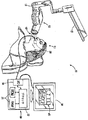
図1に、歯科X線システム10を示す。このシステムは、X線源12を含む。ここに示す実施形態では、この源は機械的アーム15の端部13上に配置される。X線源12は、起動されたとき、X線ストリーム16を発生する。(もちろん、X線は、一般に目に見えないが、ストリームの表現は、本発明の理解を容易にするために示されている)。いくつかの応用においては、X線ストリームをX線センサに位置合わせするのに役立てるために、取り外し可能なコリメータが機械的な位置決め装置とともに使用される。
FIG. 1 shows a
図1に示すように、アーム15は、口内センサ20にX線ストリームを方向づけるように、(たとえば、オペレータによって)位置決めされる。口内センサ20は、患者21の口内に配置されているのを示す。いくつかの実施形態では、口内センサ20は、X線の放射線を可視光線に変換するシンチレータと、その可視光線を電子に変換する光検出素子とを含む。他の実施形態では、センサ20は、シンチレータなしで、X線を電子に変換するように構成される。
As shown in FIG. 1, the
図2を参照すると、もっともよく分かるように、センサ20は、画素のアレイ22も含む。各画素は、その上に衝突する(シンチレータからの)光に、またはX線の放射線に応答して、電気信号を生成する。一実施形態では、センサ20は、画素が発生したアナログ信号をデジタル信号に変換する、1つまたは複数のアナログ・デジタル(「A/D」)変換器を含む。これらの信号は、プロセッサ23(プログラマブルエレクトロニックマイクロプロセッサ、FPGA、ASICまたは同様のデバイスなど)に送られる。いくつかの実施形態では、A/D変換器は、画素アレイ22の一部分として、プロセッサ23の一部分として、または画素アレイ22とプロセッサ23の間にある別の構成要素として、実装される。ここに示す実施形態では、プロセッサ23は、メモリ24(ROMおよびRAM)および入出力インターフェース25に接続される。また、センサ20は、電源を供給し、画素アレイを駆動し、出力部(たとえば、入出力インターフェース25中に配置された回路)を駆動するために、1つまたは複数の電子回路を含んでいる。アレイ22は、画素アレイ22と構成要素23、24および25との間の接続の説明を容易にするために、センサ20の一部分だけをカバーするものとして示してある。しかし、アレイ22は、ほとんどの応用の場合、センサ20と一般に同一の広がりを有し、構成要素23、24および25は、(図2に示すように)アレイ22の側面にではなく、むしろアレイ22の背後に配置される。
Referring to FIG. 2, as best seen,
図1に戻ってそれを参照すると、センサ20は、そのワイヤ、ケーブルまたは同様のコネクタ27によって、コンピュータ30に接続される。コンピュータ30は、プロセッサまたは同様の電子デバイス32、入出力インターフェース34、およびメモリ36(たとえば、RAMおよびROM)を含む、様々な構成要素を含む。1つの具体的な実施形態では、入出力インターフェース34は、ユニバーサルシリアルバス(「USB」)接続部であり、コネクタ27は、USBケーブルである。他の実施形態では、無線接続部が、センサ20とコンピュータ30の間に構成される。図1に、センサ20が取り込み、コンピュータ30が処理した画像データが、ディスプレイ38に送られて、画像40として見られることを示す。(画像40は、X線画像が通常見えるよりもっとはっきりと描画される)。
Referring back to FIG. 1, the
図3に、画素アレイ22の例示の図を表す。画素アレイ22は、説明の目的で、3×3の画素アレイとして表現されているが、画素アレイ22は、一般に9個より多くの画素を有している。画素アレイ22は、画素42と、リセットスイッチ44と、検知スイッチ45とを含む。各画素は、リセット/検知スイッチ46と、積分素子48と、読み出し増幅器50と、読み出しスイッチ52とを含む。積分素子48は、X線、暗電流およびノイズに基づくエネルギーの受け取りに応答して電荷を積分し、以下にもっと詳細に述べる。この説明において電荷という用語を使用するが、大まかに言って、電荷は、積分素子48で受け取られたエネルギーの量を表す。他の実施形態では、電子、正孔、または他の電気的信号であり、アナログであろうとデジタルあろうと、積分素子48で受け取られたエネルギーの量を表す。また、各画素は、行選択信号54および列選択信号56の1つを受け取る。行選択ライン54は、読み出しスイッチ52を制御する。各積分素子48上に蓄えられた電荷は、行選択信号54および列選択信号56を使用して読み出し、解釈して、上記に述べたようにX線画像40を生成することができる。いくつかの実施形態では、積分素子48は、読み出し時に消去される(「破壊」読み出し)。他の実施形態では、積分素子48は、読み出し時に消去されない(「非破壊」読み出し)。
FIG. 3 illustrates an exemplary diagram of the
画素アレイ22は、4つの一般的な機能状態、すなわち1)リセット状態、2)検出状態、3)積分状態、および4)読み出し状態を有する。リセット状態では、各画素42の積分素子48上に蓄えられた電荷が、積分素子48を基準電圧(たとえば、2ボルト)にセットすることによって、除去される。積分素子48は、検知スイッチ45および読み出しスイッチ52を開のままにしながら、リセット/検知スイッチ46およびリセットスイッチ44を閉じることによって、基準電圧にセットされる。
The
検出状態では、リセット/検知スイッチ46および検知スイッチ45が閉じられて、積分素子48を検知ライン47に接続し、一方リセットスイッチ44および読み出しスイッチ52が開のままにされる。検出状態では、閾値を横切ったかどうかを判定するために画素アレイの全体的な電荷が測定され、それによりX線の放射線の受け取りを示すことができる。各積分素子48は、リセット状態から、ほぼ基準電圧に等しい電圧を有して始まる。その後、電荷が、積分素子48においてX線エネルギー、暗電流およびノイズから積分されるにつれて、積分素子48における電圧が低下する。したがって、いずれかの積分素子48における電圧が低下するにつれ、検知ライン47とグラウンド59の間で測定された画素アレイ全体にわたる全体的な電圧(画素アレイ22の全体をメタダイオードとして見なすことができるので、「ダイオード電圧」という)は低下する。いくつかの実施形態では、画素42の一部分だけが、検出状態中、検知スイッチ45に接続される。他の実施形態では、追加の検知スイッチ45が画素アレイ22中に設けられ、各検知スイッチ45は画素42の特定の部分に接続される。したがって、画素アレイ22を全体にわたって検知することとは対照的に、画素42の特定の部分によって電圧閾値を横切ったことを検知することができる。
In the detection state, the reset /
積分状態では、すべてのスイッチ(44、45、46および52)が開である。画素アレイ22は、X線の放射線によって、さらには望ましくないノイズ成分(たとえば、暗電流)によって生成された電荷を積分する。
In the integrated state, all switches (44, 45, 46 and 52) are open. The
読み出し状態では、信号が、列選択ライン56(j、j+1、またはj+2のいずれか)に送られる。さらに、信号が、行選択ライン54(i、i+1、またはi+2のいずれか)に沿って画素の特定の行に送られる。それに応じて、画素の選択された行の読み出しスイッチが閉じられる。画素の行の積分素子48上に蓄えられた電荷は、出力経路57に沿って出力される。特定の列選択ライン56に送られた指示は、出力経路57の1つを選ぶように働き、選ばれた出力経路57に沿って出力された電荷をA/D変換器58に入力することが可能になる。A/D変換器58は、画素から受け取ったアナログ信号を変換して、プロセッサ23にデジタル信号を出力する。適切な行選択ライン54および列選択ライン56に信号を送ることを通じた各画素42についてのこのプロセスを繰り返すことによって、すべての画素アレイ22が読み出される。
In the read state, a signal is sent to the column select line 56 (either j, j + 1, or j + 2). In addition, a signal is sent along a row select line 54 (either i, i + 1, or i + 2) to a particular row of pixels. In response, the readout switch for the selected row of pixels is closed. The charge stored on the
いくつかの実施形態では、複数の画素が並行して読み出される。たとえば、いくつかの実施形態では、A/D変換器58は、画素42からの複数のアナログ信号をデジタル信号に同時に変換して、そのデジタル信号をマルチビットバスに沿ってプロセッサ23に転送する。他の実施形態では、個々の画素のA/D変換器が、単一のA/D変換器58とは対照的に、各画素内に設けられる。いくつかの実施形態では、積分素子48で積分された電荷によって、各積分素子にわたって蓄えられた電圧が、(低下するよりむしろ)上昇する。この実施形態では、リセット信号が、各積分素子48の間の電圧をグラウンドにセットすることによって、各積分素子48上に蓄えられた電荷を除去する。さらに、ダイオード電圧は、画素アレイがX線の放射線、暗電流および他のノイズに曝されたとき、低下するよりむしろ上昇する。したがって、閾値電圧は、リセット値より高い値にセットされ、ダイオード電圧が閾値より高いレベルまで上昇したとき、横切られる。
In some embodiments, multiple pixels are read out in parallel. For example, in some embodiments, A /
図4に、源12がX線ストリーム16を放射し、センサ20がそのX線ストリームを検出し、プロセッサ23が画像を取り込むことに対する時間軸80を表す。時刻82の前に、画素アレイ22は、リセット状態と検出状態の間で繰り返し切り替えられることによって、準備がされる。時刻82で、源12がX線ストリーム16の放射を始める。時刻84で、センサ20が、X線ストリーム16を検出し、X線ストリーム16に応答して生成される電荷の積分を始める。時刻86で、源12から放射されたX線の放射が終了する。時刻86と88の間で、画素アレイ22は、積分状態のままである。いくつかの実施形態では、X線情報が失われることになる、読み出しが早すぎることを回避するために、時刻86と88の間に積分時間が含められる。時刻88で、画素アレイ22で積分された電荷は、プロセッサ23が読み出して、いくつかの実施形態では、メモリ24に記憶される。一実施形態では、時刻82と84の間の期間は1から6ミリ秒の範囲内であり、時刻84と86の間の期間は20から600ミリ秒の範囲内であり、時刻86と88の間の期間は約2万ミリ秒の範囲内であり、時刻88と画素の読み出し終了の間の期間は約1秒である。一般に、時刻84と88の間の積分期間は、源12がX線の放射線を放射する時間の長さより長くセットされる。しかし、いくつかの実施形態では、センサ20は、回路またはソフトウェアを設けてX線放射の終了を検出し、そして時刻88で始まる読み出し動作は時刻86の前でX線放射の終了のより近くで行われる。
FIG. 4 represents a time axis 80 for
画素アレイ22の画素で受け取られた信号は、2つの主な部分、すなわちバックグラウンド信号と、X線の放射線の入射の結果として生成された信号とを含む。バックグラウンド信号は、ほとんど、1)暗電流、2)他のパラメータおよび3)ノイズの結果である。画素アレイ22におけるそれらの信号の合計がトリガー閾値レベルを横切ったとき、センサ20は、以下に述べるようにX線を検出する、または、X線が受け取られたかどうかを判定するために、追加のステップを実施する。
The signal received at the pixels of the
図5に、画素アレイ22の単一の画素(u、v)によるX線蓄積および信号出力のモデル90を示す。画素上に蓄積された電荷は、3つの成分、すなわち1)源12からのX線信号92、それは、シンチレータまたは同様のデバイスによって光に変換することができ、2)様々な源からのランダムノイズ94、および3)暗電流96を含む。その3つの成分は画素で積分され、その機能は積分器98で表される。積分器98は、図3に積分素子48として表す。画素は、一実施形態ではCMOSデバイスであり、ブロック100において積分された電荷を電圧に変換する。ブロック100は、図3に読み出し増幅器50として表す。その後、画素の読み出しが、画素アレイの列を読み出し、その後行を読み出すことによって、ステップ104および106で行われる。あるいは、行が読み出され、その後列が読み出される。列と行の順序にかかわらず、画素アレイ22から読み出された電圧は、A/D変換器108によって変換され、A/D変換器108は、画素アレイ内にまたは画素アレイ22の外部にあることができる。A/D変換器108は、図3にA/D変換器58として示す。また、ブロック102a〜cに、画素アレイがランダムノイズを受ける恐れがあることを示しているが、その影響は、通常無視してよい。A/D変換器108の前で、A/D変換器108の内部で、またはデジタル的にA/D変換器108の後で、信号に利得を加えることができる。
FIG. 5 shows a model 90 of X-ray accumulation and signal output by a single pixel (u, v) of the
図6に、半導体撮像の分野では知られている、暗電流に及ぼす温度の影響を示す。センサ20の画素アレイ22の温度が、(特定の部分上で、または全体的に)上昇するにつれて、暗電流は増加する。たとえば、暗電流は、ほぼ7〜11℃ごとに2倍になる。画素アレイ22の温度は、たとえば、口内のX線のために患者の口の内部に配置されると上昇することがあり、日光に曝されると上昇することがあり、あるいは、消毒剤(アルコールなど)に曝されると低下することがある。暗電流は、その蓄積が許容されている場合、最終的に画素アレイ22のトリガー閾値を横切り、X線が受け取られていないときに画像取り込みをトリガーしてしまうことになる。
FIG. 6 shows the effect of temperature on dark current, which is known in the field of semiconductor imaging. As the temperature of the
図7および8に、暗電流の蓄積によって画素アレイ22が誤ってトリガーされることを防止するプロセス150、および固定リセットのタイミング図151aおよび151bを表す。このプロセスは、ステップ152で始まり、リセットステップ154に進む。リセットステップ154では、変数「t」が0にリセットされ、画素アレイ22がリセットされる。画素アレイ22をリセットするために、電荷が、上記に図3を参照して述べたように、それぞれの画素から流出させられる。リセットの後、電荷は、暗電流またはX線ストリーム16などの源から蓄積を始める。ステップ156で、プロセスは変数tが所定の「リセット時間」に等しいかどうかを判定する。変数tがリセット時間に等しくない場合、プロセスは、ステップ158に進む。ステップ158で、プロセスは画素アレイ22中に蓄積された電荷がトリガー閾値を超えたかどうかを判定する。そうでない場合、プロセスは、ステップ160に進み、そこで変数tが1だけ増加する(すなわち、t=t+1)。
7 and 8 represent a
ステップ160の後、プロセスはステップ156に戻り、再び、変数tがリセット時間に等しいかどうかを判定する。X線ストリーム16が、所定の期間(リセット時間)にわたって画素アレイ22で受け取られていない場合、プロセスのステップ156〜160は十分な回数だけ繰り返され、それによって、ステップ156でtはリセット時間に等しくなることになる。次いで、処理はリセットステップ154に進み、画素アレイ22はリセットされ、暗電流による電荷は取り除かれる。プロセスは、ステップ156〜160に戻り、X線ストリーム16の受け取りを待つ。例示のリセット時間は、約1ミリ秒とすることができる。リセット時間は、センサ20の製造中に、またはセンサ20の取り付け前の別のときに(取り付けは、センサがユーザのコンピュータ30に接続されるときに行われる)、プロセッサ23中に記憶してもよい。いくつかの実施形態では、リセット時間は、異なるX線の放射線量に適合するように、および、センサ20の経年劣化および用途の一方又は双方を考慮するように、現場で更新される。
After
ステップ158で、画素アレイ22中に蓄積された電荷がトリガー閾値を超えた場合、プロセス150は、X線ストリーム16が画素アレイ22によって受け取られたと判定する。その後、ステップ162で画素アレイ22はプロセッサ23によって読み出され、ステップ164でコンピュータ30に出力される。
In step 158, if the charge accumulated in the
図8に、リセット信号181(リセットステップ154中に画素アレイ22に送られる)および画素アレイ22中への電荷の蓄積に対するタイミング図151aおよび151bを表す。電荷が画素アレイ22中で蓄積されるにつれて、ダイオード電圧182は初期値から下降する。タイミング図151aに示すように、リセット時間が過ぎた後に(t=ステップ156におけるリセット時間)X線ストリーム16が画素アレイによって受け取られていないと仮定されると、リセット信号がパルスされ、画素アレイ22がリセットされる。しかしながら、X線ストリーム16が受け取られた場合、タイミング図151bに示すように、ダイオード電圧はより早く低下して、閾値電圧183より下を横切り、X線ストリーム16が検出されることになる(ステップ158)。図8に示す実施形態では、300マイクロ秒のリセット時間、0.5Vの閾値電圧183、および2Vの初期電圧が使用される。他の実施形態では、異なる値を使用することができる。
FIG. 8 depicts timing diagrams 151a and 151b for the reset signal 181 (sent to the
図7の固定タイミングのプロセス150はいくつかの事例でうまくゆくが、より適応性のある技術を使用することができる。選ばれたリセット時間が長すぎる場合、暗電流が蓄積されて、X線ストリームが受け取られていないときに画像の取り込みをトリガーすることになる。選ばれたリセット時間が短すぎる場合、X線の放射線の受け取りを知らせるのに十分な電荷を画素アレイ22で積分することができないことになる。したがって、トリガー閾値は横切られず、X線ストリーム16は検出されないことになる。さらに、リセット時間は、動作中、異なる環境設定に合わせて自動的に調節することができない。たとえば、図6に示すように、暗電流は温度に大きく依存する。温度変動の可能性があるために、リセット時間を適切に選択することの困難さが増加される。さらに、第1の設定で適切なリセット時間は、第2の設定では適切でないことがある。1つの追加の問題は、源12、源12とセンサ20の間の距離、および源12とセンサ20の位置合わせに依存して、異なる量の放射線が放射される場合があるということである。そのため、リセット時間は、蓄積された暗電流による誤ったトリガーを回避するのに十分短く、X線の放射線の低放射線量に適合するのに十分長くなければならない。
The fixed
図9および10に、これらの問題に対処する適応タイミングプロセス250を表す(図10に、タイミング図251を表し、それは、以下で述べる)。図9のプロセス250は、ステップ252で始まり、リセットステップ254に進む。リセットステップ254では、変数iが0にリセットされ、リセット信号256をパルスすることによって、画素アレイ22がリセットされる。リセットステップの後、センサは、ダイオード電圧258がステップ262でトリガー閾値260を横切るまで、暗電流を蓄積することが可能である。カウンタがリセットステップ254と暗電流によってトリガー閾値260を横切るまでとの間のクロックパルス264の数を数えて、t0=クロックパルス264の数とセットする。この値t0は、初期暗電流トリガー時間である。また、値tiは「時系列」として参照される。
FIGS. 9 and 10 represent an
プロセス250はステップ266に進み、そこで、リセット信号256をパルスすることによって画素アレイが再びリセットされ、i=i+1とセットされる。ステップ268で、プロセス250はトリガー値270が論理ハイに変化したかどうかを判定することによって、トリガー閾値を横切ったかどうかを判定する。ステップ268は、トリガー値270が論理ハイに変えられるまで繰り返される。トリガー値270が論理ハイになったとき、ステップ272で、ti=リセットステップ266から経過したクロックパルス264の数とセットされる。ステップ276で、TAVG(i=0からiまでのtiの移動平均)が計算される。さらに、時刻i=0からiまでのTAVGの標準偏差が、ステップ276で計算される。TAVGは、平均暗電流トリガー時間を表す。この平均暗電流トリガー時間は、画素アレイ22のリセットと、ダイオード電圧の暗電流による閾値260の横切りとの間の平均経過時間である。いくつかの実施形態では、TAVGは、単にti−1に等しくセットされるか、または前のti値の最大数(たとえば、i=i−20からiのti)だけについてのtiの移動平均である。
その後、ステップ278で、TAVG−tiがTAVGの標準偏差の倍数と比較される。TAVG−tiがTAVGの標準偏差のn倍より大きい場合、X線が検出される。微調整変数「n」の値は、検出プロセスを調節するように選択される。いくつかの実施形態では0<n<1であり、TAVGからの小さな変動からX線が検出されることになることを意味する。他の実施形態では、n>1であり、TAVGからの大きな変動の場合だけ、X線が検出されることになる。さらに他の実施形態ではn=1であり、標準偏差より大きいいかなるTAVGからの変動の場合もX線が検出されることになる。X線の検出のとき、プロセス250は、ステップ280に進み、そこで画素アレイ22がプロセッサ23によって読み出されて、ステップ282でコンピュータ30に出力される。しかし、ステップ278で、ti−TAVGがnとTAVGの標準偏差の積より小さい場合、プロセスはステップ266に戻り、画素アレイをリセットしi=i+1とセットする。
Thereafter, at step 278, T AVG -t i is compared with a multiple of the standard deviation of T AVG. T AVG -t i cases n times larger than the standard deviation of T AVG, X-rays are detected. The value of the fine tuning variable “n” is selected to adjust the detection process. In some embodiments, 0 <n <1, meaning that X-rays will be detected from small variations from TAVG . In other embodiments, n> 1 and X-rays will be detected only in the case of large variations from TAVG . In yet other embodiments and n = 1, so that X-rays are detected in the case of change from a larger standard deviation any T AVG. Upon detection of x-rays,
いくつかの実施形態では、ステップ278の比較は、TAVGとtiの間の差を所定値(たとえば、0、1、2など)と比較するだけである。TAVGとtiの間の差が所定値より大きい場合、方法250によってX線がセンサ20で受け取られたと判定する。
In some embodiments, the comparison of step 278, a predetermined value the difference between T AVG and t i (e.g., 0,1,2, etc.) is only compared. If the difference between T AVG and t i is greater than a predetermined value,
他の実施形態では、ステップ276は複数のサブステップ(示さず)に置き換えられ、各サブステップは、TAVGとtiの間の差と、ユニークな所定値(たとえば、0、1、2など)または動的な値(標準偏差)との比較を含む。複数の比較を使用すると、プロセス250によって、1)高線量率、短い持続期間のX線露光、および2)低線量率、長い持続期間のX線露光の両方を検出することが可能になる。高線量率、短い持続期間の露光を検出するために、1つのサブステップは、もっとも最近のti値だけに焦点を合わせた検出アルゴリズムを含むことができる。低線量率、長い持続期間の露光を検出するために、他のサブステップは、より長い期間にわたってti値を解析する検出アルゴリズムを含むことができる。サブステップは並列に実行され、いずれかのサブステップがX線の検出されたことを示した場合、プロセス250はステップ280に進む。たとえば、変数Xが変数Yより大きい場合、高線量率、短い持続期間の露光を検出するための第1のサブステップは、TAVGとtiの間の差がXより大きい場合にX線を検出することができる。低線量率、長い持続期間の露光を検出するための第2のサブステップは、TAVGとtiの間の差、TAVGとti−1の間の差、TAVGとti−2の間の差、TAVGとti−3の間の差、およびTAVGとti−4の間の差がすべてYより大きい場合に、X線を検出することができる。XおよびYは、所定の静的な値か、またはTAVGの標準偏差などの動的な値にある程度基づいたものでよいが、様々な微調整変数nを使用してもよい。第3のサブステップは、tiとti−1の間の差が変数Zより大きいことを判定するだけでX線を示すことができる。この第3のサブステップでは、変数Zは、単にノイズによって引き起こされたいかなる起こり得る変動よりも大きくなるように、比較的大きくすべきである。
In other embodiments,
いくつかの実施形態では、ステップ262および268はタイムアウト限界を有し、それによって、センサ20が閾値260を横切らない場合、所定の時間の経過後にタイムアウト信号を発生する。したがって、タイムアウト限界は、エラーによって閾値260を横切ることが防止されたときに、センサ20が無限の時間待つことを防止する。
In some embodiments,
いくつかの実施形態では、TAVGまたはtiの値は、センサ20が過熱状態である(たとえば、直射日光に曝されたために)ことを示すものとして、プロセッサ23が使用する。たとえば、暗電流によってダイオード電圧が閾値260を一度横切った場合、または所定回数繰り返し横切った場合のいずれかにおいて、TAVGが低すぎる場合、プロセッサ23はセンサ20が過熱していると判断を下す。センサ20が過熱していると検出されたとき、適切な警戒信号、警報または他の情報がユーザに提供される。
In some embodiments, the value of T AVG or t i is used by the
ここで、図10を参照すると、タイミング図251にはトリガー値270が含まれ、それは、ダイオード電圧258がトリガー閾値260を横切ったことを示す。たとえば、クロックパルス264を数えることによって時間が測定される。次いで、変数tiが、プロセス250について述べたように、数えられたクロックパルスの数にセットされる。リセット信号256がパルスされ、画素アレイ22をリセットし、ダイオード電圧258をリセットする。図10に示す実施形態では、0.5Vのトリガー閾値260、2Vの初期ダイオード電圧258が使用される。他の実施形態では、異なる値が使用される。
Referring now to FIG. 10, the timing diagram 251 includes a
プロセス250のいくつかの実施形態では、センサ20は準備完了状態または待機状態になるように構成される。センサ20が待機状態であるとき、プロセス250は、ステップ278での判定が誤りであると常に判定されることを除いて正常に進み、このプロセスはTAVG、ti、n、およびTAVGの標準偏差の値にかかわらずステップ266に戻る。センサ20が準備完了であるとき、ステップ278での判定は正常に実行される(TAVG−tiが調整変数nとTAVGの標準偏差の積より大きい場合、プロセスは、ステップ280に進む)。しかし、センサ20が待機していた間に計算された値は、継続して準備完了の状態で使用される。
In some embodiments of
いくつかの実施形態では、一定利得レベルが画素アレイ22から出力されたデータに適用される。利得レベルは、ダイオード電圧258の変化率259を変更する(図10参照)。たとえば、利得レベルがより高いと変化率259が増加し、それによって、閾値電圧260を横切らせるために積分素子48におけるより小さな電荷積分が必要となる。対照的に、利得レベルがより低いと変化率259が低下し、それによって、閾値電圧260を横切らせるために積分素子48におけるより大きな電荷積分が必要となる。いくつかの実施形態では、利得レベルはtiレベルに基づき変更される。たとえば、tiレベルが短すぎる場合、利得レベルは低下して、平均暗電流時間を増加させることがある。一般に、その結果には、X線がセンサで受け取られたとき、TAVG(平均暗電流時間)とti値の間の差がより大きくなることが含まれる。tiレベルが長すぎる場合、利得レベルは増加し、X線関連の電荷は十分に積分されて、ノイズの低いX線画像を生成することができる。
In some embodiments, a constant gain level is applied to the data output from the
いくつかの実施形態では、プロセス250で計算された平均暗電流トリガー時間は、プロセッサ23が使用してセンサ20が動作している温度を見積もる。計算された温度は、特に、センサ20の温度記録を生成し、センサ20が許容温度範囲外の温度で動作していることをユーザに警告するために使用することができる。温度記録はセンサ20に課された熱ストレス(たとえば、センサに消毒剤を吹き付けることによって生じるストレス)を同定するために、または他の保全解析のために使用される。さらに、計算された温度は、センサ20のオフセット画像を縮小拡大すること、センサ20のオフセット画像を予測すること、またはその両方に使用することができる。
In some embodiments, the average dark current trigger time calculated in
他の実施形態では、画素アレイ22に対する所望の積分時間が、画素アレイ22のリセットと、(方法250によって判定される)画素アレイ22でのX線の受け取りまでの間の時間tiを解析することによって見積もられる。時間tiは、線量率を見積もるために解析される。tiがより短いと、見積もられた線量率はより高くなる。というのは、閾値を横切るためにかかる時間の長さが短いからである。線量率の見積もりがいったん決定されると、積分時間(すなわち、図4の時刻84と88の間の時間)は適切に調節することができる。たとえば、プロセッサ23が高線量率を見積もった場合、より短い積分時間が使用される。プロセッサ23が低線量率を見積もった場合、より長い積分時間が使用される。正確に見積もられた線量率に基づき積分時間を調節すると、画素アレイ22中の暗電流は長い積分時間のためにより少なくなり、その上、余りにも早くX線信号の積分を中断する短い積分時間を防止する。
In other embodiments, the desired integration time for the
プロセス150および250は、画素アレイ22の全体にわたって蓄積された電荷に基づく検出プロセスを使用する。画素アレイ全体上の電荷の測定はいくつかの状況下では適切な検出を提供するが、蓄積された電荷の積分レベルは、X線の場が画素アレイ22全体をカバーしない場合、変化する。X線の場が画素アレイ22全体をカバーしないとき(「円錐カット(cone cut)」としても参照される)、X線による積分量はカバーされていなかった画素アレイ22の部分に比例して減少するが、暗電流の作用は、それでも画素アレイ22全体にわたって積分される。したがって、X線は、X線源が画素アレイ22に適切に位置合わせされていない場合検出されない恐れがある。たとえば、図11aでは、X線源12は適切に位置合わせされており、画素アレイ22はX線ストリーム16の円400内に完全に含まれる。しかし、図11bおよび11cでは、X線ストリーム16の円400は画素アレイ22の全体には達していない。むしろ、画素アレイの一部分だけがX線の放射線を受け取っている。画素アレイ22の全体より小さい部分でX線の放射線を受け取っている場合、画素アレイ22上に蓄積される電荷量は、(たとえば、図11aに示すように)円400内に画素アレイ全体が含まれる場合より少なくなる。したがって、図11bおよび11cでは、X線の放射線を受けたにもかかわらず、トリガー閾値を横切らない恐れがある。
位置合わせ不良のX線源に配慮するために、いくつかの実施形態では、検出プロセス150および250は画素アレイ22の複数の区域を別々にモニタする。たとえば、図11a〜cの画素アレイ22は14個の区域を含み、例示の目的で、その4つは区域402、404、406および408と名付ける。したがって、X線が、それらの区域のいずれかで検出された場合、プロセスは画素アレイ22全体でX線を検出して、画像取り込みを行う。したがって、自動的な検出プロセスは、X線源12およびセンサ20の位置合わせ不良に配慮している。
To account for misaligned x-ray sources, in some embodiments, detection processes 150 and 250 monitor multiple areas of
いくつかの実施形態では、別々にモニタされている画素アレイ22の複数の区域の1つまたは複数は、X線検出の後に検出モードの状態に保たれ、一方画素アレイ22の区域の残りは積分モードに切り替えられる。検出モードのままであるいくつかの区域からもたらされた情報は、1)誤トリガーが行われなかったことを確認する、2)A/CのX線パルスパターンを検出する、および3)画素アレイ22で受け取られているX線放射の終了を検出するために使用することができる。上記に述べたように、X線放射の終了の検出は、画素アレイ22の積分の持続期間をX線露光の持続期間により厳密に合わせるために使用することができる。積分の持続期間をより厳密に合わせることは、X線露光の持続期間をより厳密に合わせるように時刻84と88の間の期間を減少させる。
In some embodiments, one or more of the plurality of areas of the
上記に述べた検出プロセスはヒトの歯科に向けられているが、いくつかの実施形態では、このプロセスは、獣医学の用途、歯以外の用途、および無生物の撮像を対象としたX線センサとともに使用される。さらに、いくつかの実施形態では、センサ20のプロセッサ23およびメモリ24、またはそれらの付随する機能は、コンピュータ30に属しているか、またはその中で実行される。
Although the detection process described above is directed to human dentistry, in some embodiments, the process is used with x-ray sensors for veterinary applications, non-dental applications, and inanimate imaging. used. Further, in some embodiments, the
タイミング図およびプロセスは、具体的な論理状態、たとえば論理ハイおよび論理ローを用いて述べたが、本発明の実施形態では、同様の事象を信号で伝えるために、代替の信号の位置付けの使用が意図される。たとえば、トリガー値270は、ダイオード電圧258が図10のトリガー閾値260を横切ったときに論理ハイになる。しかし、いくつかの実施形態では、トリガー値270はトリガー閾値260を横切ったことを示すために論理ローになる。
Although the timing diagrams and processes have been described using specific logic states, such as logic high and logic low, embodiments of the present invention allow the use of alternative signal positioning to signal similar events. Intended. For example, the
したがって、本発明は、とりわけ、X線を自動的に検出するためのシステムおよび方法を提供する。本発明の様々な特徴および効果は、以下の特許請求の範囲で述べる。 Accordingly, the present invention provides, among other things, a system and method for automatically detecting x-rays. Various features and advantages of the invention are set forth in the following claims.
10 歯科X線システム
12 X線源
13 端部
15 機械的アーム
16 X線ストリーム
20 口内センサ、センサ
21 患者
22 画素アレイ
23 プロセッサ
24 メモリ
25 入出力インターフェース
30 コンピュータ
32 プロセッサまたは同様の電子デバイス
34 入出力インターフェース
36 メモリ
38 ディスプレイ
40 X線画像
42 画素
44 リセットスイッチ
45 検知スイッチ
46 リセット/検知スイッチ
47 検知ライン
48 積分素子
50 読み出し増幅器
52 読み出しスイッチ
54 行選択信号、行選択ライン
56 列選択信号、列選択ライン
57 出力経路
58 A/D変換器
80 時間軸
82、84、86、88 時刻
90 モデル
92 X線信号
94 ランダムノイズ
96 暗電流
98 積分器
100 ブロック
102a、102b、102c ブロック
108 A/D変換器
181 リセット信号
182 ダイオード電圧
183 閾値電圧
256 リセット信号
258 ダイオード電圧
259 変化率
260 トリガー閾値、閾値電圧
264 クロックパルス
270 トリガー値
400 円
402、404、406、408 区域
DESCRIPTION OF
Claims (22)
蓄えられた電荷を画素アレイから除去することによって、前記画素アレイをリセットするステップと、
平均暗電流トリガー時間を求めるステップと、
前記画素アレイのリセットからの経過時間を測定するステップと、
前記経過時間と平均暗電流トリガー時間との比較を行うステップと、
閾値を横切ったことを判定するステップであって、前記閾値を横切ることは、所定量の電荷が、前記画素アレイの少なくとも一部分上に蓄えられたことを示す、ステップと、
X線の放射線が、前記画素アレイの前記少なくとも一部分で受け取られたことを、前記比較に基づき判定するステップと、
X線の放射線が受け取られたと判定されたとき、X線画像を生成するのに使用するために、前記画素アレイからデータを出力するステップと
を含み、前記平均暗電流トリガー時間は、前記画素アレイのリセットと前記閾値の横切りとの間の平均時間を含む、方法。 A method for detecting X-ray radiation using an X-ray sensor,
Resetting the pixel array by removing stored charge from the pixel array;
Obtaining an average dark current trigger time;
Measuring an elapsed time since reset of the pixel array;
Comparing the elapsed time with an average dark current trigger time;
Determining that a threshold has been crossed, wherein crossing the threshold indicates that a predetermined amount of charge has been stored on at least a portion of the pixel array; and
Determining, based on the comparison, that x-ray radiation has been received at the at least a portion of the pixel array;
Outputting data from the pixel array for use in generating an X-ray image when it is determined that X-ray radiation has been received, wherein the average dark current trigger time is determined by the pixel array Including an average time between resetting and crossing the threshold.
所定値と、
微調整変数と前記平均暗電流トリガー時間の標準偏差との積と
のうちの少なくとも1つにも基づく、請求項1に記載の方法。 The step of comparing the elapsed time and the average dark current trigger time includes:
A predetermined value,
The method of claim 1, wherein the method is also based on at least one of a product of a fine tuning variable and a standard deviation of the average dark current trigger time.
前記画素アレイの前記少なくとも一部分上に蓄えられた前記所定量の電荷によって、ダイオードでの電位が前記閾値より低くなる、請求項1から6のうちの何れか一項に記載の方法。 The threshold is a predetermined voltage level;
7. A method according to any one of the preceding claims, wherein the predetermined amount of charge stored on the at least part of the pixel array causes a potential at a diode to be lower than the threshold.
前記比較を行うステップは、前記経過時間と前記平均暗電流トリガー時間との間の差を第1の値と比較するステップを含み、
前記判定演算を実行するステップは、
前記差を第2の値と比較するステップと、
前の経過時間と前の平均暗電流トリガー時間との間の第2の差を、前記第2の値と比較するステップと
を含む、請求項1から7のうちの何れか一項に記載の方法。 Further comprising performing a decision operation using the elapsed time and the average dark current trigger time;
Performing the comparison includes comparing a difference between the elapsed time and the average dark current trigger time to a first value;
The step of executing the determination calculation includes:
Comparing the difference with a second value;
And comparing a second difference between a previous elapsed time and a previous average dark current trigger time with the second value. Method.
前記第1の値は、前記第2の値より大きい、請求項9に記載の方法。 1) If the difference is greater than the first value, determine that a high dose rate has occurred; 2) If both the difference and the second difference are greater than the second value, low dose Further comprising determining that the rate has occurred,
The method of claim 9, wherein the first value is greater than the second value.
前記画素アレイのリセットと前記X線の放射線が前記画素アレイの前記少なくとも一部分で受け取られたときとの間の測定された経過時間に基づき、その後のX線の放射線の露光に対する積分時間を減少又は増大させるステップとをさらに含む、請求項1から10のうちの何れか一項に記載の方法。 Determining that the x-ray radiation has been received;
Decrease integration time for subsequent X-ray radiation exposure based on measured elapsed time between reset of the pixel array and when the X-ray radiation is received at the at least a portion of the pixel array, or 11. The method according to any one of claims 1 to 10, further comprising an increasing step.
プロセッサと、
画素アレイと、
メモリと
を含み、
前記プロセッサは、
蓄えられた電荷を前記画素アレイから除去することによって、前記画素アレイをリセットし、
平均暗電流トリガー時間を求め、
前記画素アレイのリセットからの経過時間を測定し、
前記経過時間と平均暗電流トリガー時間との比較を行い、
閾値を横切ったことを判定し、前記閾値を横切ることは、所定量の電荷が前記画素アレイの少なくとも一部分上に蓄えられたことを示し、
X線の放射線が前記画素アレイの前記少なくとも一部分で受け取られたことを、前記比較に基づき判定し、
X線の放射線が受け取られたと判定されたとき、X線画像を生成するのに使用するために、前記画素アレイからデータを出力する
ように構成され、前記平均暗電流トリガー時間は、前記画素アレイのリセットと前記閾値の横切りとの間の平均時間を含む、X線センサ。 An X-ray sensor for detecting receipt of X-rays,
A processor;
A pixel array;
Including memory,
The processor is
Resetting the pixel array by removing stored charge from the pixel array;
Find the average dark current trigger time,
Measure the elapsed time from reset of the pixel array,
Compare the elapsed time and the average dark current trigger time,
Determining that the threshold has been crossed, crossing the threshold indicates that a predetermined amount of charge has been stored on at least a portion of the pixel array;
Determining, based on the comparison, that x-ray radiation has been received at the at least a portion of the pixel array;
When it is determined that X-ray radiation has been received, the pixel array is configured to output data from the pixel array for use in generating an X-ray image; X-ray sensor comprising an average time between resetting and crossing the threshold.
所定値と、
微調整変数と前記平均暗電流トリガー時間の標準偏差との積と
のうちの少なくとも1つにも基づいて行うように、さらに構成された、請求項12に記載のX線センサ。 The processor compares the elapsed time with the average dark current trigger time.
A predetermined value,
The X-ray sensor according to claim 12, further configured to perform based on at least one of a product of a fine tuning variable and a standard deviation of the average dark current trigger time.
前記画素アレイの前記少なくとも一部分上に蓄えられた前記所定量の電荷によって、ダイオードでの電位が前記閾値より低くなる、請求項12から17のうちの何れか一項に記載のX線センサ。 The threshold is a predetermined voltage level;
18. The X-ray sensor according to claim 12, wherein the predetermined amount of electric charge stored on the at least part of the pixel array causes a potential at a diode to be lower than the threshold value. 19.
前記比較を行うことは、前記経過時間と前記平均暗電流トリガー時間との間の差を第1の値と比較することを含み、
前記判定演算を実行することは、前記差を第2の値と比較することと、前の経過時間と前の平均暗電流トリガー時間との間の第2の差を、前記第2の値と比較することとを含む、請求項12から18のうちの何れか一項に記載のX線センサ。 The processor is further configured to perform a decision operation using the elapsed time and the average dark current trigger time;
Making the comparison includes comparing a difference between the elapsed time and the average dark current trigger time to a first value;
Performing the determination operation may include comparing the difference with a second value and calculating a second difference between a previous elapsed time and a previous average dark current trigger time to the second value. The X-ray sensor according to claim 12, comprising comparing.
前記第1の値は、前記第2の値より大きい、請求項20に記載のX線センサ。 The processor 1) determines that a high dose rate has occurred if the difference is greater than the first value, and 2) both the difference and the second difference are greater than the second value. Is further configured to determine that a low dose rate has occurred,
The X-ray sensor according to claim 20, wherein the first value is larger than the second value.
前記X線の放射線が受け取られたことを判定し、
前記画素アレイのリセットと前記X線の放射線が前記画素アレイの前記少なくとも一部分で受け取られたときとの間の測定された経過時間に基づき、その後のX線の放射線の露光に対する積分時間を減少又は増大させるようにさらに構成された、請求項12から21のうちの何れか一項に記載のX線センサ。 The processor is
Determining that the X-ray radiation has been received;
Decrease integration time for subsequent X-ray radiation exposure based on measured elapsed time between reset of the pixel array and when the X-ray radiation is received at the at least a portion of the pixel array, or 22. X-ray sensor according to any one of claims 12 to 21, further configured to increase.
Applications Claiming Priority (2)
| Application Number | Priority Date | Filing Date | Title |
|---|---|---|---|
| US10855208P | 2008-10-27 | 2008-10-27 | |
| US61/108,552 | 2008-10-27 |
Publications (3)
| Publication Number | Publication Date |
|---|---|
| JP2010099481A JP2010099481A (en) | 2010-05-06 |
| JP2010099481A5 JP2010099481A5 (en) | 2012-11-01 |
| JP5769921B2 true JP5769921B2 (en) | 2015-08-26 |
Family
ID=42016980
Family Applications (1)
| Application Number | Title | Priority Date | Filing Date |
|---|---|---|---|
| JP2009246319A Expired - Fee Related JP5769921B2 (en) | 2008-10-27 | 2009-10-27 | System and method for X-ray detection by a sensor |
Country Status (5)
| Country | Link |
|---|---|
| US (3) | US8119990B2 (en) |
| EP (1) | EP2180343B1 (en) |
| JP (1) | JP5769921B2 (en) |
| KR (1) | KR101719814B1 (en) |
| IL (1) | IL201765A (en) |
Cited By (1)
| Publication number | Priority date | Publication date | Assignee | Title |
|---|---|---|---|---|
| KR101870610B1 (en) | 2017-05-24 | 2018-06-25 | 주식회사 센소니아 | Trigger circuit of x-ray photographing device improving stability to change in temperature with controlling reset peroid |
Families Citing this family (32)
| Publication number | Priority date | Publication date | Assignee | Title |
|---|---|---|---|---|
| US9492129B2 (en) * | 2008-10-27 | 2016-11-15 | Dental Imaging Technologies Corporation | Triggering of intraoral X-ray sensor using pixel array sub-sampling |
| US8366318B2 (en) | 2009-07-17 | 2013-02-05 | Dental Imaging Technologies Corporation | Intraoral X-ray sensor with embedded standard computer interface |
| JP5464064B2 (en) * | 2010-06-09 | 2014-04-09 | コニカミノルタ株式会社 | Portable radiographic imaging device and radiographic imaging system |
| JP5475574B2 (en) * | 2010-07-02 | 2014-04-16 | 富士フイルム株式会社 | Radiation detection element and radiographic imaging device |
| JP2012083307A (en) * | 2010-10-14 | 2012-04-26 | Fujifilm Corp | Radiation detection device, radiation image photographing system, radiation detection program and radiation detection method |
| JP5209021B2 (en) | 2010-10-19 | 2013-06-12 | 富士フイルム株式会社 | Radiation image capturing apparatus, radiation image capturing system, radiation image capturing program, and radiation image capturing method |
| JP5289477B2 (en) * | 2011-02-09 | 2013-09-11 | 富士フイルム株式会社 | Radiation image detection apparatus and radiation irradiation start detection method |
| US8729485B2 (en) | 2012-02-17 | 2014-05-20 | Luxen Technologies, Inc. | Parallel mode readout integrated circuit for X-ray image sensor |
| US9128195B2 (en) | 2012-03-28 | 2015-09-08 | Luxen Technologies, Inc. | Increasing dynamic range for x-ray image sensor |
| US20130256542A1 (en) | 2012-03-28 | 2013-10-03 | Luxen Technologies, Inc. | Programmable readout integrated circuit for an ionizing radiation sensor |
| US8942444B2 (en) | 2012-08-17 | 2015-01-27 | General Electric Company | System and method for image compression in X-ray imaging systems |
| KR101389525B1 (en) * | 2012-12-20 | 2014-04-25 | 아스텔 주식회사 | X-ray detector apparatus, x-ray image taking system using the x-ray detector apparatus |
| US9113827B2 (en) * | 2013-01-17 | 2015-08-25 | Jordan C. Christoff | Intraoral X-ray imaging device with optimized image data output |
| US9788809B2 (en) * | 2013-03-06 | 2017-10-17 | Canon Kabushiki Kaisha | Apparatus, method and computer-readable medium storing program for radiographic imaging with elapsed time control of radiation sensor apparatus |
| KR102025928B1 (en) * | 2013-05-14 | 2019-09-26 | 삼성전자주식회사 | Imaging apparatus and controlling method thereof |
| KR102208106B1 (en) * | 2014-04-03 | 2021-01-28 | 주식회사 레이언스 | Imaging system including image sensor and method of driving the same |
| JP6491432B2 (en) * | 2014-08-08 | 2019-03-27 | キヤノン株式会社 | Radiation imaging apparatus and control method thereof |
| FR3025086B1 (en) | 2014-09-02 | 2016-11-11 | E2V Semiconductors | METHOD AND SYSTEM FOR TAKING MEDICAL RADIOLOGICAL IMAGES WITH STOP CONTROL OF THE X-RAY SOURCE |
| KR20160048538A (en) | 2014-10-24 | 2016-05-04 | 삼성전자주식회사 | Apparatus and method for detecting X-ray, X-ray imaging system |
| KR101687522B1 (en) | 2015-06-25 | 2016-12-20 | 주식회사 뷰웍스 | X-ray detector |
| CN105496444B (en) * | 2015-12-01 | 2018-06-26 | 苏州佳世达光电有限公司 | Scan control method and scanning means |
| FR3046679B1 (en) | 2016-01-12 | 2019-12-27 | Teledyne E2V Semiconductors Sas | X-RAY DETECTION CIRCUIT FOR DENTAL RADIOLOGICAL SENSOR |
| US10213180B2 (en) * | 2016-09-14 | 2019-02-26 | Dental Imaging Technologies Corporation | Multiple-dimension imaging sensor with operation based on magnetic field detection |
| US10299742B2 (en) * | 2016-09-14 | 2019-05-28 | Dental Imaging Technologies Corporation | Multiple-dimension imaging sensor with fault condition detection |
| US10932733B2 (en) | 2016-09-14 | 2021-03-02 | Dental Imaging Technologies Corporation | Multiple-dimension imaging sensor with operation based on movement detection |
| US10299741B2 (en) * | 2016-09-14 | 2019-05-28 | Dental Imaging Technologies Corporation | Multiple-dimension imaging sensor and state-based operation of an imaging system including a multiple-dimension imaging sensor |
| JP6412208B2 (en) * | 2017-05-25 | 2018-10-24 | 富士フイルム株式会社 | Radiation image capturing apparatus, radiation image capturing system, radiation image capturing program, and radiation image capturing method |
| KR101855658B1 (en) * | 2017-05-26 | 2018-06-08 | 주식회사 센소니아 | Trigger circuit of x-ray photographing device having trigger valid peroid |
| EP3677100A2 (en) * | 2017-09-02 | 2020-07-08 | Cetteen GmbH | Control device for an x-ray tube and method for operating an x-ray tube |
| US11191497B2 (en) * | 2018-10-16 | 2021-12-07 | Shayda Cullen | Digital dental x-ray sensor device having a rounded housing including a radio transceiver |
| JP7392289B2 (en) * | 2019-05-22 | 2023-12-06 | コニカミノルタ株式会社 | Radiation image detection device |
| US11911197B2 (en) * | 2021-12-14 | 2024-02-27 | BAE Systems Imaging Solutions Inc. | X-ray sensor system for intraoral tomography |
Family Cites Families (99)
| Publication number | Priority date | Publication date | Assignee | Title |
|---|---|---|---|---|
| DE2519640C3 (en) | 1975-05-02 | 1981-02-05 | Siemens Ag, 1000 Berlin Und 8000 Muenchen | Dental X-ray diagnostic device with means for measuring the recording time |
| US4057732A (en) | 1976-02-04 | 1977-11-08 | Rolf Marcus Klauser | Film holder for bite-wing radiographs |
| US4259583A (en) | 1979-05-03 | 1981-03-31 | Albert Richard D | Image region selector for a scanning X-ray system |
| FR2547495B1 (en) | 1983-06-16 | 1986-10-24 | Mouyen Francis | APPARATUS FOR OBTAINING A DENTAL RADIOLOGICAL IMAGE |
| US4866750A (en) | 1987-03-27 | 1989-09-12 | Board Of Regents, The University Of Texas System | Image receptor holder and bite block device |
| DE8909398U1 (en) | 1989-08-03 | 1989-10-05 | Siemens Ag, 1000 Berlin Und 8000 Muenchen, De | |
| SE469104B (en) | 1991-06-03 | 1993-05-10 | Regam Medical Systems Ab | PROCEDURE AND DEVICE FOR X-ray apparatus with electronic image detection |
| US5331166A (en) | 1991-10-25 | 1994-07-19 | Kabushiki Kaisha Morita Seisakusho | Dental X-ray image detecting device with an automatic exposure function |
| DE4218020C1 (en) | 1992-06-01 | 1993-07-15 | Siemens Ag, 8000 Muenchen, De | |
| JP3190458B2 (en) | 1992-10-15 | 2001-07-23 | 浜松ホトニクス株式会社 | Dental X-ray image processing device |
| US5434418A (en) | 1992-10-16 | 1995-07-18 | Schick; David | Intra-oral sensor for computer aided radiography |
| DE4402114C2 (en) | 1994-01-25 | 1999-06-02 | Sirona Dental Systems Gmbh | Radiation detector with a housing for receiving a radiation converter |
| US5471515A (en) | 1994-01-28 | 1995-11-28 | California Institute Of Technology | Active pixel sensor with intra-pixel charge transfer |
| JPH08603A (en) | 1994-06-24 | 1996-01-09 | Morita Mfg Co Ltd | Medical x-ray image detecting device |
| US5574250A (en) | 1995-02-03 | 1996-11-12 | W. L. Gore & Associates, Inc. | Multiple differential pair cable |
| US5757011A (en) | 1995-02-10 | 1998-05-26 | Orbit Semiconductor, Inc. | X-ray onset detector and method |
| US5510623A (en) | 1995-02-24 | 1996-04-23 | Loral Fairchild Corp. | Center readout intra-oral image sensor |
| DE29505854U1 (en) | 1995-04-05 | 1995-06-01 | Pfeiffer Manfred Dr | Device for image acquisition in the oral area, in particular for dental diagnosis |
| SE9501332L (en) | 1995-04-10 | 1996-10-11 | Regam Medical Systems Ab | Device at CCD cell |
| DE29506839U1 (en) | 1995-04-22 | 1995-06-22 | Pfeiffer Manfred Dr | Sensor that can be placed intraorally of a patient's mouth to create a patient's tooth / jaw images |
| GB2303772B (en) | 1995-07-28 | 1999-06-16 | Eev Ltd | Imaging apparatus |
| GB9515762D0 (en) | 1995-08-01 | 1995-10-04 | Eev Ltd | Imaging apparatus |
| JP3441578B2 (en) | 1995-11-22 | 2003-09-02 | 株式会社モリタ製作所 | Dental panoramic radiography device |
| US6127684A (en) * | 1996-02-26 | 2000-10-03 | Canon Kabushiki Kaisha | Photoelectric conversion apparatus and driving method of the apparatus |
| EP0792066B1 (en) * | 1996-02-26 | 2004-11-03 | Canon Kabushiki Kaisha | Photoelectric conversion apparatus and driving method thereof |
| US5887049A (en) | 1996-11-12 | 1999-03-23 | California Institute Of Technology | Self-triggered X-ray sensor |
| US6011251A (en) | 1997-06-04 | 2000-01-04 | Imec | Method for obtaining a high dynamic range read-out signal of a CMOS-based pixel structure and such CMOS-based pixel structure |
| JPH10277028A (en) | 1997-04-08 | 1998-10-20 | Morita Mfg Co Ltd | Dental x-ray image detector and adapter therefor |
| JP3836208B2 (en) | 1997-04-09 | 2006-10-25 | 浜松ホトニクス株式会社 | Small medical X-ray image detection device |
| US5912942A (en) | 1997-06-06 | 1999-06-15 | Schick Technologies, Inc. | X-ray detection system using active pixel sensors |
| DE29717432U1 (en) | 1997-09-30 | 1999-02-04 | Sirona Dental Sys Gmbh & Co Kg | Sensor that can be placed intraorally of a patient's mouth to create a patient's tooth / jaw images |
| US6462268B1 (en) | 1998-08-06 | 2002-10-08 | Krone, Inc. | Cable with twisting filler and shared sheath |
| US6134298A (en) | 1998-08-07 | 2000-10-17 | Schick Technologies, Inc. | Filmless dental radiography system using universal serial bus port |
| US6033111A (en) | 1998-11-20 | 2000-03-07 | Wolf X-Ray Corporation | Color coding method and apparatus for an X-ray positioning system |
| US6203195B1 (en) | 1999-01-20 | 2001-03-20 | Timothy G. Willis | Holder for dental sensors |
| JP2002543684A (en) * | 1999-04-26 | 2002-12-17 | シマゲ オユ | Self-triggered imaging device for radiation imaging lines |
| DE60010703T2 (en) | 1999-06-30 | 2005-05-19 | Dentsply International Inc. | Positioning device for various dental X-ray recording methods with a sensor holder and different bite blocks of modular design |
| US6244866B1 (en) | 1999-12-29 | 2001-06-12 | Regina Campbell | Tongue suppressing bite block |
| WO2001058148A1 (en) | 2000-02-02 | 2001-08-09 | Dentsply International Inc. | Automatic x-ray detection for intra-oral dental x-ray imaging apparatus |
| JP4234304B2 (en) | 2000-05-19 | 2009-03-04 | 浜松ホトニクス株式会社 | Radiation detector |
| JP4398065B2 (en) | 2000-05-19 | 2010-01-13 | 浜松ホトニクス株式会社 | Radiation detector |
| US6307915B1 (en) * | 2000-06-26 | 2001-10-23 | Afp Imaging Corporation | Triggering of solid state X-ray imagers with non-destructive readout capability |
| US6527442B2 (en) | 2000-06-26 | 2003-03-04 | Afp Imaging Corporation | Integrated sensor holder for dental imaging |
| US6320934B1 (en) | 2000-06-26 | 2001-11-20 | Afp Imaging Corporation | Sensor characterization in memory |
| US6404854B1 (en) | 2000-06-26 | 2002-06-11 | Afp Imaging Corporation | Dental x-ray imaging system |
| DE20100641U1 (en) | 2001-01-27 | 2001-07-26 | Steer Sebastian | Universally adjustable holder system for easy positioning of a recording medium for X-rays |
| SE0100382D0 (en) | 2001-02-07 | 2001-02-07 | Lp Roentgenteknik Ab | X-ray detector |
| DE50106886D1 (en) | 2001-05-05 | 2005-09-01 | Pfeiffer Manfred | Apparatus for image acquisition in the oral field, in particular for dental diagnosis |
| FI117818B (en) | 2001-08-03 | 2007-03-15 | Palodex Group Oy | Irradiation control in an X-ray imaging device used for intraoral application |
| JP3950665B2 (en) * | 2001-10-23 | 2007-08-01 | キヤノン株式会社 | Radiation imaging apparatus and imaging method of radiation imaging apparatus |
| JP3778844B2 (en) | 2001-11-15 | 2006-05-24 | 浜松ホトニクス株式会社 | Image sensor and imaging system using the image sensor |
| US6652141B1 (en) | 2002-01-24 | 2003-11-25 | Cygnus Technologies, L.L.C. | Intraoral sensor |
| US6811312B2 (en) | 2002-02-08 | 2004-11-02 | Schick Technologies, Inc. | Dental x-ray positioning using adhesives |
| ITBO20020440A1 (en) | 2002-07-05 | 2004-01-05 | Cefla Coop | UNIT FOR THE ACQUISITION AND VISUALIZATION OF DENTAL RADIOGRAPHIC IMAGES |
| US7072443B2 (en) | 2002-10-03 | 2006-07-04 | Schick Technologies, Inc. | Intraoral image sensor |
| US6972411B2 (en) | 2002-10-03 | 2005-12-06 | Schick Technologies, Inc. | Method of event detection for intraoral image sensor |
| US6924486B2 (en) | 2002-10-03 | 2005-08-02 | Schick Technologies, Inc. | Intraoral sensor having power conservation features |
| US7033075B2 (en) | 2002-11-27 | 2006-04-25 | Op-D-Op, Inc. | Apparatus for retaining a radiographic sensor during dental x-ray imaging |
| EP1605829B1 (en) | 2003-03-24 | 2017-06-14 | Kaltenbach & Voigt GmbH | Intraoral x-ray sensor |
| DE10313976A1 (en) | 2003-03-27 | 2004-10-28 | Sirona Dental Systems Gmbh | Image receiver for creating digital dental images |
| FR2857160B1 (en) | 2003-07-01 | 2005-09-23 | Atmel Grenoble Sa | ERGONOMIC IMAGE SENSOR |
| US7661880B2 (en) | 2003-07-17 | 2010-02-16 | Calderwood Mitchell C | Radiographic sensor positioning system |
| TWM243182U (en) | 2003-09-03 | 2004-09-11 | Ying-Chau Yau | Multi-directional bracketed tooth X-ray radiation clamp |
| ES2298485T3 (en) | 2003-11-21 | 2008-05-16 | Carestream Health, Inc. | DENTAL RADIOLOGY DEVICE. |
| EP1537826B1 (en) | 2003-11-26 | 2010-11-10 | Carestream Health, Inc. | Method of signal processing in a dental radiologic apparatus |
| US7006600B1 (en) | 2004-01-15 | 2006-02-28 | Progeny, Inc. | Integrated digital dental x-ray system |
| US7036985B2 (en) | 2004-02-25 | 2006-05-02 | Ultradent Products, Inc. | X-ray positioning device |
| US7090395B2 (en) | 2004-04-05 | 2006-08-15 | Dov Glazer | Wireless digital dental x-ray sensor with positioning apparatus |
| US6974253B2 (en) | 2004-04-12 | 2005-12-13 | Instrumentarium Corp. | Connection between X-ray sensor and holder |
| SE528307C2 (en) | 2004-07-06 | 2006-10-17 | Unident Ab | Device at container |
| FI119008B (en) | 2004-07-22 | 2008-06-13 | Planmeca Oy | Wireless intraoral X-ray imaging |
| US7172339B2 (en) | 2004-07-26 | 2007-02-06 | Jennifer A Diederich | Intraoral dental radiology positioning device for use with aiming ring |
| ATE346546T1 (en) | 2004-08-06 | 2006-12-15 | Gendex Corp | IMAGE SENSOR FOR DENTAL INTRAORAL X-RAY RADIOGRAPHY |
| DE102004046968A1 (en) | 2004-09-28 | 2006-04-06 | Siemens Ag | Detector system, in particular for intraoral X-ray images |
| JP5236951B2 (en) | 2005-02-16 | 2013-07-17 | デンツプライ インターナショナル インコーポレーテッド | General-purpose dental X-ray sensor holder |
| US20060188070A1 (en) | 2005-02-23 | 2006-08-24 | Razzano Michael R | Image capture device and methods |
| US7195395B2 (en) | 2005-02-28 | 2007-03-27 | Kerrhawe Sa | Dental sensor clamp |
| US20060199146A1 (en) | 2005-03-01 | 2006-09-07 | Schick Technologies | Method of transferring power and data via an inductive link |
| GB0504415D0 (en) | 2005-03-03 | 2005-04-06 | E2V Tech Uk Ltd | Non-planar x-ray sensor |
| FR2883719B1 (en) | 2005-04-01 | 2007-06-01 | Atmel Grenoble Soc Par Actions | INTRAORAL DENTAL IMAGE SENSOR AND RADIOLOGICAL SYSTEM USING THE SENSOR |
| US7775713B2 (en) | 2005-05-16 | 2010-08-17 | Palodex Group Oy | Arrangement for dental imaging |
| FR2888044B1 (en) | 2005-07-01 | 2007-08-31 | Atmel Grenoble Soc Par Actions | IMAGE SENSOR WITH CORNERS |
| GB0514998D0 (en) | 2005-07-21 | 2005-08-31 | E2V Tech Uk Ltd | Sensor with trigger pixels for imaging of pulsed radiation |
| CA2619528C (en) | 2005-08-16 | 2013-11-26 | Dentsply International Inc. | Holder device for dental x-ray digital sensor |
| US7425095B2 (en) | 2005-08-23 | 2008-09-16 | Harold K. Schmulenson | Instrument for holding and aligning an x-ray sensing device |
| US7563026B2 (en) | 2005-09-08 | 2009-07-21 | Schick Technologies, Inc. | Flexible intra-oral x-ray imaging device |
| US7501631B2 (en) | 2005-10-07 | 2009-03-10 | Schick Technologies, Inc. | Shielding an imaging array from X-ray noise |
| US20070147675A1 (en) | 2005-12-06 | 2007-06-28 | Johannes Ulrici | Image detection system, comprising an X-ray sensor and an image detecting unit, and method of operating same |
| CA2653837C (en) | 2006-05-30 | 2015-08-04 | Dentsply International Inc. | Adjustable dental x-ray image media holder |
| JP2006263483A (en) * | 2006-06-06 | 2006-10-05 | Canon Inc | Imaging device |
| US7659516B2 (en) | 2006-06-29 | 2010-02-09 | Dalsa Corporation | C-MOS sensor readout from multiple cells across the array to generate dose sensing signal |
| FR2908625B1 (en) | 2006-11-17 | 2008-12-26 | E2V Semiconductors Soc Par Act | MULTI-LED INTRAORAL DENTAL IMAGE SENSOR SYSTEM |
| US7959355B2 (en) | 2006-11-19 | 2011-06-14 | George Stantchev | Method and apparatus for imaging using digital dental X-ray sensor |
| JP5217156B2 (en) * | 2006-11-29 | 2013-06-19 | コニカミノルタエムジー株式会社 | Radiation imaging system |
| US8876375B2 (en) | 2007-02-22 | 2014-11-04 | Dentsply International Inc. | Color coded dental X-ray positioning device |
| JP5105940B2 (en) * | 2007-04-06 | 2012-12-26 | キヤノン株式会社 | Imaging apparatus, imaging system, control method thereof, and program |
| US20090108311A1 (en) | 2007-10-25 | 2009-04-30 | Xinqiao Liu | CMOS Detector with Reduced Sensitivity to X-Rays |
| US7605376B2 (en) | 2007-10-29 | 2009-10-20 | Fairchild Imaging, Inc. | CMOS sensor adapted for dental x-ray imaging |
| US7812879B2 (en) * | 2007-10-30 | 2010-10-12 | Fairchild Imaging | Self-triggering CMOS image sensor |
-
2009
- 2009-10-26 US US12/605,624 patent/US8119990B2/en not_active Expired - Fee Related
- 2009-10-26 EP EP09174091.0A patent/EP2180343B1/en active Active
- 2009-10-26 IL IL201765A patent/IL201765A/en active IP Right Grant
- 2009-10-27 JP JP2009246319A patent/JP5769921B2/en not_active Expired - Fee Related
- 2009-10-27 KR KR1020090102361A patent/KR101719814B1/en active IP Right Grant
-
2012
- 2012-01-25 US US13/358,125 patent/US8324587B2/en active Active
- 2012-12-03 US US13/692,323 patent/US20130092844A1/en not_active Abandoned
Cited By (1)
| Publication number | Priority date | Publication date | Assignee | Title |
|---|---|---|---|---|
| KR101870610B1 (en) | 2017-05-24 | 2018-06-25 | 주식회사 센소니아 | Trigger circuit of x-ray photographing device improving stability to change in temperature with controlling reset peroid |
Also Published As
| Publication number | Publication date |
|---|---|
| US20120119099A1 (en) | 2012-05-17 |
| EP2180343B1 (en) | 2018-07-25 |
| US8324587B2 (en) | 2012-12-04 |
| IL201765A0 (en) | 2010-06-16 |
| JP2010099481A (en) | 2010-05-06 |
| KR20100047167A (en) | 2010-05-07 |
| IL201765A (en) | 2013-06-27 |
| US8119990B2 (en) | 2012-02-21 |
| EP2180343A2 (en) | 2010-04-28 |
| KR101719814B1 (en) | 2017-03-24 |
| US20100102241A1 (en) | 2010-04-29 |
| US20130092844A1 (en) | 2013-04-18 |
| EP2180343A3 (en) | 2013-05-29 |
Similar Documents
| Publication | Publication Date | Title |
|---|---|---|
| JP5769921B2 (en) | System and method for X-ray detection by a sensor | |
| KR101749777B1 (en) | Triggering of intraoral x-ray sensor using pixel array sub-sampling | |
| US9675307B2 (en) | Radiation imaging apparatus, radiation imaging system, and control method of radiation imaging system | |
| US10585196B2 (en) | Radiation detection apparatus for changing sensitivity of radiation sensing during control for radiation imaging, method of controlling the same, and non-transitory computer-readable storage medium | |
| KR101919619B1 (en) | Radiographic detector including trap occupancy change monitor and feedback, imaging apparatus and methods using the same | |
| JPH09133772A (en) | Image forming device | |
| JP6797909B2 (en) | Polarization correction for direct conversion X-ray detector | |
| JP2003299641A (en) | Method for identifying and correcting pixel having excess pixel lag in semiconductor x-ray detector | |
| EP3348049B1 (en) | Radiation detector and x-ray imaging system | |
| JP2017530565A (en) | Radiation detector and radiography method using the same | |
| US7847261B2 (en) | Radiation detector | |
| EP3300665A1 (en) | Imager with bump detection | |
| JP7266052B2 (en) | Intraoral imaging system and imaging device | |
| JPS592077B2 (en) | Smoke detectors | |
| KR20230145339A (en) | intraoral imaging device | |
| JP2007243527A (en) | Sample timing monitor system | |
| JP2010154985A (en) | Mastication frequency detecting device |
Legal Events
| Date | Code | Title | Description |
|---|---|---|---|
| A621 | Written request for application examination |
Free format text: JAPANESE INTERMEDIATE CODE: A621 Effective date: 20120523 |
|
| A521 | Request for written amendment filed |
Free format text: JAPANESE INTERMEDIATE CODE: A523 Effective date: 20120914 |
|
| A977 | Report on retrieval |
Free format text: JAPANESE INTERMEDIATE CODE: A971007 Effective date: 20130523 |
|
| A131 | Notification of reasons for refusal |
Free format text: JAPANESE INTERMEDIATE CODE: A131 Effective date: 20130527 |
|
| A601 | Written request for extension of time |
Free format text: JAPANESE INTERMEDIATE CODE: A601 Effective date: 20130826 |
|
| A602 | Written permission of extension of time |
Free format text: JAPANESE INTERMEDIATE CODE: A602 Effective date: 20130829 |
|
| A521 | Request for written amendment filed |
Free format text: JAPANESE INTERMEDIATE CODE: A523 Effective date: 20131126 |
|
| A131 | Notification of reasons for refusal |
Free format text: JAPANESE INTERMEDIATE CODE: A131 Effective date: 20140305 |
|
| A601 | Written request for extension of time |
Free format text: JAPANESE INTERMEDIATE CODE: A601 Effective date: 20140530 |
|
| A602 | Written permission of extension of time |
Free format text: JAPANESE INTERMEDIATE CODE: A602 Effective date: 20140604 |
|
| A521 | Request for written amendment filed |
Free format text: JAPANESE INTERMEDIATE CODE: A523 Effective date: 20140905 |
|
| A131 | Notification of reasons for refusal |
Free format text: JAPANESE INTERMEDIATE CODE: A131 Effective date: 20150216 |
|
| A521 | Request for written amendment filed |
Free format text: JAPANESE INTERMEDIATE CODE: A523 Effective date: 20150424 |
|
| RD04 | Notification of resignation of power of attorney |
Free format text: JAPANESE INTERMEDIATE CODE: A7424 Effective date: 20150511 |
|
| TRDD | Decision of grant or rejection written | ||
| A01 | Written decision to grant a patent or to grant a registration (utility model) |
Free format text: JAPANESE INTERMEDIATE CODE: A01 Effective date: 20150526 |
|
| A61 | First payment of annual fees (during grant procedure) |
Free format text: JAPANESE INTERMEDIATE CODE: A61 Effective date: 20150624 |
|
| R150 | Certificate of patent or registration of utility model |
Ref document number: 5769921 Country of ref document: JP Free format text: JAPANESE INTERMEDIATE CODE: R150 |
|
| R250 | Receipt of annual fees |
Free format text: JAPANESE INTERMEDIATE CODE: R250 |
|
| R250 | Receipt of annual fees |
Free format text: JAPANESE INTERMEDIATE CODE: R250 |
|
| R250 | Receipt of annual fees |
Free format text: JAPANESE INTERMEDIATE CODE: R250 |
|
| R250 | Receipt of annual fees |
Free format text: JAPANESE INTERMEDIATE CODE: R250 |
|
| LAPS | Cancellation because of no payment of annual fees |