EP2180343B1 - System and method of x-ray detection with a sensor - Google Patents
System and method of x-ray detection with a sensor Download PDFInfo
- Publication number
- EP2180343B1 EP2180343B1 EP09174091.0A EP09174091A EP2180343B1 EP 2180343 B1 EP2180343 B1 EP 2180343B1 EP 09174091 A EP09174091 A EP 09174091A EP 2180343 B1 EP2180343 B1 EP 2180343B1
- Authority
- EP
- European Patent Office
- Prior art keywords
- pixel array
- ray
- dark current
- sensor
- difference
- Prior art date
- Legal status (The legal status is an assumption and is not a legal conclusion. Google has not performed a legal analysis and makes no representation as to the accuracy of the status listed.)
- Active
Links
- 238000000034 method Methods 0.000 title claims description 63
- 238000001514 detection method Methods 0.000 title description 17
- 230000005855 radiation Effects 0.000 claims description 49
- 230000010354 integration Effects 0.000 claims description 20
- 230000008569 process Effects 0.000 description 38
- 238000010586 diagram Methods 0.000 description 12
- 238000003384 imaging method Methods 0.000 description 8
- 230000007423 decrease Effects 0.000 description 7
- 210000000214 mouth Anatomy 0.000 description 7
- 238000009825 accumulation Methods 0.000 description 5
- 230000004913 activation Effects 0.000 description 4
- 230000004044 response Effects 0.000 description 4
- 230000003044 adaptive effect Effects 0.000 description 3
- 230000008859 change Effects 0.000 description 3
- 230000000694 effects Effects 0.000 description 3
- 230000001186 cumulative effect Effects 0.000 description 2
- 230000001419 dependent effect Effects 0.000 description 2
- 239000000645 desinfectant Substances 0.000 description 2
- 230000001066 destructive effect Effects 0.000 description 2
- 230000006870 function Effects 0.000 description 2
- 238000009434 installation Methods 0.000 description 2
- 230000002829 reductive effect Effects 0.000 description 2
- LFQSCWFLJHTTHZ-UHFFFAOYSA-N Ethanol Chemical compound CCO LFQSCWFLJHTTHZ-UHFFFAOYSA-N 0.000 description 1
- 230000003213 activating effect Effects 0.000 description 1
- 230000002411 adverse Effects 0.000 description 1
- 210000003484 anatomy Anatomy 0.000 description 1
- 230000002238 attenuated effect Effects 0.000 description 1
- 230000015572 biosynthetic process Effects 0.000 description 1
- 210000000988 bone and bone Anatomy 0.000 description 1
- 238000010276 construction Methods 0.000 description 1
- 230000003247 decreasing effect Effects 0.000 description 1
- 230000007613 environmental effect Effects 0.000 description 1
- 230000002431 foraging effect Effects 0.000 description 1
- 230000008571 general function Effects 0.000 description 1
- 230000036541 health Effects 0.000 description 1
- 238000012423 maintenance Methods 0.000 description 1
- 238000004519 manufacturing process Methods 0.000 description 1
- 230000007246 mechanism Effects 0.000 description 1
- 238000012544 monitoring process Methods 0.000 description 1
- 230000036961 partial effect Effects 0.000 description 1
- 230000002028 premature Effects 0.000 description 1
- 238000012545 processing Methods 0.000 description 1
- 238000012552 review Methods 0.000 description 1
- 239000004065 semiconductor Substances 0.000 description 1
- 238000005507 spraying Methods 0.000 description 1
- 230000003068 static effect Effects 0.000 description 1
- 230000035882 stress Effects 0.000 description 1
- 230000008646 thermal stress Effects 0.000 description 1
- 210000001519 tissue Anatomy 0.000 description 1
- 230000001960 triggered effect Effects 0.000 description 1
Images


Classifications
-
- A—HUMAN NECESSITIES
- A61—MEDICAL OR VETERINARY SCIENCE; HYGIENE
- A61B—DIAGNOSIS; SURGERY; IDENTIFICATION
- A61B6/00—Apparatus or devices for radiation diagnosis; Apparatus or devices for radiation diagnosis combined with radiation therapy equipment
- A61B6/50—Apparatus or devices for radiation diagnosis; Apparatus or devices for radiation diagnosis combined with radiation therapy equipment specially adapted for specific body parts; specially adapted for specific clinical applications
- A61B6/51—Apparatus or devices for radiation diagnosis; Apparatus or devices for radiation diagnosis combined with radiation therapy equipment specially adapted for specific body parts; specially adapted for specific clinical applications for dentistry
-
- H—ELECTRICITY
- H01—ELECTRIC ELEMENTS
- H01L—SEMICONDUCTOR DEVICES NOT COVERED BY CLASS H10
- H01L27/00—Devices consisting of a plurality of semiconductor or other solid-state components formed in or on a common substrate
- H01L27/14—Devices consisting of a plurality of semiconductor or other solid-state components formed in or on a common substrate including semiconductor components sensitive to infrared radiation, light, electromagnetic radiation of shorter wavelength or corpuscular radiation and specially adapted either for the conversion of the energy of such radiation into electrical energy or for the control of electrical energy by such radiation
- H01L27/144—Devices controlled by radiation
- H01L27/146—Imager structures
-
- A—HUMAN NECESSITIES
- A61—MEDICAL OR VETERINARY SCIENCE; HYGIENE
- A61B—DIAGNOSIS; SURGERY; IDENTIFICATION
- A61B6/00—Apparatus or devices for radiation diagnosis; Apparatus or devices for radiation diagnosis combined with radiation therapy equipment
- A61B6/42—Arrangements for detecting radiation specially adapted for radiation diagnosis
- A61B6/4208—Arrangements for detecting radiation specially adapted for radiation diagnosis characterised by using a particular type of detector
- A61B6/4233—Arrangements for detecting radiation specially adapted for radiation diagnosis characterised by using a particular type of detector using matrix detectors
-
- G—PHYSICS
- G01—MEASURING; TESTING
- G01T—MEASUREMENT OF NUCLEAR OR X-RADIATION
- G01T1/00—Measuring X-radiation, gamma radiation, corpuscular radiation, or cosmic radiation
- G01T1/16—Measuring radiation intensity
- G01T1/17—Circuit arrangements not adapted to a particular type of detector
-
- G—PHYSICS
- G01—MEASURING; TESTING
- G01T—MEASUREMENT OF NUCLEAR OR X-RADIATION
- G01T1/00—Measuring X-radiation, gamma radiation, corpuscular radiation, or cosmic radiation
- G01T1/29—Measurement performed on radiation beams, e.g. position or section of the beam; Measurement of spatial distribution of radiation
- G01T1/2914—Measurement of spatial distribution of radiation
- G01T1/2921—Static instruments for imaging the distribution of radioactivity in one or two dimensions; Radio-isotope cameras
- G01T1/2928—Static instruments for imaging the distribution of radioactivity in one or two dimensions; Radio-isotope cameras using solid state detectors
-
- H—ELECTRICITY
- H04—ELECTRIC COMMUNICATION TECHNIQUE
- H04N—PICTORIAL COMMUNICATION, e.g. TELEVISION
- H04N23/00—Cameras or camera modules comprising electronic image sensors; Control thereof
- H04N23/30—Cameras or camera modules comprising electronic image sensors; Control thereof for generating image signals from X-rays
-
- H—ELECTRICITY
- H04—ELECTRIC COMMUNICATION TECHNIQUE
- H04N—PICTORIAL COMMUNICATION, e.g. TELEVISION
- H04N25/00—Circuitry of solid-state image sensors [SSIS]; Control thereof
- H04N25/60—Noise processing, e.g. detecting, correcting, reducing or removing noise
- H04N25/63—Noise processing, e.g. detecting, correcting, reducing or removing noise applied to dark current
-
- H—ELECTRICITY
- H04—ELECTRIC COMMUNICATION TECHNIQUE
- H04N—PICTORIAL COMMUNICATION, e.g. TELEVISION
- H04N5/00—Details of television systems
- H04N5/30—Transforming light or analogous information into electric information
- H04N5/32—Transforming X-rays
-
- A—HUMAN NECESSITIES
- A61—MEDICAL OR VETERINARY SCIENCE; HYGIENE
- A61B—DIAGNOSIS; SURGERY; IDENTIFICATION
- A61B6/00—Apparatus or devices for radiation diagnosis; Apparatus or devices for radiation diagnosis combined with radiation therapy equipment
- A61B6/50—Apparatus or devices for radiation diagnosis; Apparatus or devices for radiation diagnosis combined with radiation therapy equipment specially adapted for specific body parts; specially adapted for specific clinical applications
- A61B6/508—Apparatus or devices for radiation diagnosis; Apparatus or devices for radiation diagnosis combined with radiation therapy equipment specially adapted for specific body parts; specially adapted for specific clinical applications for non-human patients
-
- G—PHYSICS
- G03—PHOTOGRAPHY; CINEMATOGRAPHY; ANALOGOUS TECHNIQUES USING WAVES OTHER THAN OPTICAL WAVES; ELECTROGRAPHY; HOLOGRAPHY
- G03B—APPARATUS OR ARRANGEMENTS FOR TAKING PHOTOGRAPHS OR FOR PROJECTING OR VIEWING THEM; APPARATUS OR ARRANGEMENTS EMPLOYING ANALOGOUS TECHNIQUES USING WAVES OTHER THAN OPTICAL WAVES; ACCESSORIES THEREFOR
- G03B42/00—Obtaining records using waves other than optical waves; Visualisation of such records by using optical means
- G03B42/02—Obtaining records using waves other than optical waves; Visualisation of such records by using optical means using X-rays
- G03B42/04—Holders for X-ray films
- G03B42/042—Holders for X-ray films for dental applications
-
- H—ELECTRICITY
- H04—ELECTRIC COMMUNICATION TECHNIQUE
- H04N—PICTORIAL COMMUNICATION, e.g. TELEVISION
- H04N23/00—Cameras or camera modules comprising electronic image sensors; Control thereof
- H04N23/70—Circuitry for compensating brightness variation in the scene
Definitions
- the present invention relates to x-ray imaging. More particularly, embodiments of the invention relate to automatic triggering of an x-ray sensor used in dentistry.
- X-rays have been used in dentistry to image teeth and parts of the mouth for many years.
- the process involves generating x-rays outside the patient's oral cavity and directing the x-rays at an image receptor located in the patient's mouth.
- the x-rays are attenuated differently by different parts of the patient's dental structures (e.g., bone versus tissue) and this difference in attenuation is used to create an image, such as on film or by using an electronic image sensor.
- the x-ray source is triggered manually by the operator.
- the capturing of an image is initiated by a technician or other person by, for example, activating a switch.
- the image is captured as soon as the film is exposed to x-ray radiation. So, there is no need to "activate" the film. Once the x-ray source is activated and the x-rays reach the film, an image is captured.
- the particular image captured depends on at least two factors: activation of the x-ray source and "activation" of the sensor. What constitutes “activation” of the sensor can vary based upon the type of sensor used, but in most cases “activation” occurs when a command is provided to the sensor to either store or output its current image data (referred to herein as “image capture”). So, in some systems, there is an electrical link between the x-ray source and the sensor such that when the x-ray source is activated, a command is sent (simultaneously or nearly simultaneously) to the sensor to perform an image capture. Thus, it is possible to generate a burst of x-ray radiation and be assured that an image will be captured by the sensor during the relatively short period of x-ray exposure.
- the x-ray imaging system includes an x-ray image sensor having an array of pixels organized in rows and columns and carries out an image capture sequence.
- the image capture sequence includes a wait for exposure period. During the wait for exposure period the reference pixels are compared with a threshold one by one. If, after a predetermined time interval, a predetermined number of reference pixels are above the threshold, it is decided that exposure has started.
- U.S. Publication No. 2004/065836 discloses a method of determining that radiation is incident upon a radiation sensor.
- the method includes monitoring the magnitude of current drawn by each pixel of a sensor array of an intraoral sensor and generating a signal from the intraoral sensor to a base station, which is connected to a computer.
- the signal is generated when the amount of current drawn by each pixel exceeds a predetermined amount.
- U.S. Patent No. 5,694,448 discloses an imaging apparatus for use in intraoral dental applications.
- the imaging apparatus includes a charge-coupled device (CCD), which includes an array of radiation sensitive detector elements which accumulate charge depending on the intensity of the radiation directed onto the detector elements. The accumulated charge can be clocked at selected times to produce a signal S. When an x-ray pulse is applied, signal S will rise rapidly. Once the signal S rises above a reference signal, image acquisition begins.
- CCD charge-coupled device
- Embodiments of the invention provide automatic triggering of an x-ray sensor.
- the sensor detects x-ray radiation from an x-ray source without requiring that a particular trigger signal be sent to the sensor.
- no particular triggering signal is sent to an automatic x-ray sensor, some initializing signals may be sent to the sensor to activate or arm the sensor and indicate it should begin waiting to detect x-ray radiation.
- the inventors have recognized many challenges with respect to automatic triggering systems.
- One challenge relates to false triggering based on dark current accumulation.
- dark current and other noise can build charge on the sensor and, eventually, cause the sensor to incorrectly determine x-ray radiation has been received.
- This false triggering issue is amplified as the ambient temperature near the sensor increases because dark current increases with temperature.
- Another challenge associated with automatic triggering systems relates to the alignment between the x-ray source and the sensor.
- x-ray sensors particularly those placed in the mouth (i.e., an intra-oral sensor)
- x-ray sensors are often misaligned.
- only a portion of the x-ray sensor is exposed to radiation.
- this partial exposure is not sufficient to cause a simple threshold-based trigger to initiate image capture.
- a misalignment may not be recognized until the x-ray technician attempts to review images that he or she believes to have been created only to discover that no such images have been created. The technician may then try to realign the x-ray source and sensor and reinitiate the imaging process.
- Yet another challenge associated with automatic triggering systems is the relatively large variation in x-ray doses and dose rates that are provided to perform x-ray image formation in a receptor.
- the variation in dosages and dose rates is caused by a number of factors including differences in x-ray sources.
- X-ray sources are manufactured by a number of different manufacturers and their designs and specifications have changed over time. Thus, the intensity of their outputs varies. For example, older x-ray machines usually generate relatively high x-ray doses with alternating dose rates while newer machines generate lower doses with more steady dose rates.
- the variation in x-ray doses and dose rates received at the sensor is also a consequence of variations in anatomy (from patient to patient) and the distance of the source to the patient. As is known, the dose is dependent on the distance (d) between the source and the patient by a factor of d 2 .
- This disclosure provides a method of automatically detecting x-ray radiation with an x-ray sensor.
- the method includes resetting a pixel array by removing stored charge from the pixel array and measuring, by a processor, an elapsed time since resetting of the pixel array.
- the method also includes a processor executing a decision operation using the elapsed time and an average dark current trigger time, and determining that a threshold has been crossed. The threshold being crossed indicates a predetermined amount of charge has been stored on at least a portion of the pixel array.
- the method also includes determining, by the processor, that x-ray radiation has been received at a portion of the pixel array based on the decision operation. Upon determining that x-ray radiation has been received, data is output from the pixel array to be used to generate an x-ray image.
- the x-ray sensor includes a processor, a pixel array, and a memory.
- the processor is configured to reset a pixel array by removing stored charge from the pixel array and measure an elapsed time since resetting of the pixel array.
- the processor is also configured to execute a decision operation using the elapsed time and an average dark current trigger time, and to determine that a threshold has been crossed.
- the threshold being crossed indicates a predetermined amount of charge has been stored on at least a portion of the pixel array.
- the processor is configured to determine that x-ray radiation has been received at a portion of the pixel array based on the decision operation. Upon determining that x-ray radiation has been received, the processor is configured to output data from the pixel array to be used to generate an x-ray image.
- processor as is used in this application to mean any of a microcontroller, programmable logic device (e.g., a field programmable gate array "FPGA”), a general purpose processor, specifically designed hardware (e.g., an application specific integrated circuit "ASIC”), or a combination thereof.
- programmable logic device e.g., a field programmable gate array "FPGA”
- FPGA field programmable gate array
- ASIC application specific integrated circuit
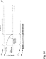
- Fig. 1 illustrates a dental x-ray system 10.
- the system includes an x-ray source 12.
- the source is located on an end 13 of a mechanical arm 15.
- the x-ray source 12 When activated, the x-ray source 12 generates an x-ray stream 16.
- x-rays are generally invisible, but a representation of a stream is illustrated to facilitate understanding of the invention.
- a removable collimator is used with a mechanical positioning device to help align the x-ray stream with an x-ray sensor.
- the arm 15 is positioned (e.g., by an operator) so that the x-ray stream is directed to an intraoral sensor 20.
- the intraoral sensor 20 is shown located in the mouth of a patient 21.
- the intraoral sensor 20 includes a scintillator that coverts x-ray radiation to visible light and light detecting elements that convert the visible light to electrons.
- the sensor 20 is configured to convert x-rays to electrons without a scintillator.
- the sensor 20 also includes an array of pixels 22. Each pixel produces an electric signal in response to light (from the scintillator) or x-ray radiation impinged upon it.
- the sensor 20 includes one or more analog-to-digital (“A/D") converters to covert analog signals generated by the pixels to digital signals. These signals are provided to a processor 23 (such as a programmable, electronic microprocessor, FPGA, ASIC, or similar device).
- the A/D converters are implemented as part of the pixel array 22, as part of the processor 23, or as separate components between the pixel array 22 and the processor 23.
- the processor 23 is connected to memory 24 (ROM and RAM) and an input-output interface 25.
- the sensor 20 also includes one or more electronic circuits for power supply, driving the pixel array, and driving the output (e.g., circuits located in the I/O interface 25).
- the array 22 is shown as covering only a portion of the sensor 20. However, in most applications, the array 22 is generally coextensive with the sensor 20 and the components 23, 24, and 25 are located behind the array 22, rather than to the side of the array 22 (as shown in Fig. 2 ).
- a wire, cable, or similar connecter 27 of the sensor 20 connects the sensor 20 to a computer 30.
- the computer 30 includes various components, including a processor or similar electronic device 32, an input/output interface 34, and memory 36 (e.g., RAM and ROM).
- the input/output interface 34 is a Universal Serial Bus ("USB") connection and the connector 27 is a USB cable.
- USB Universal Serial Bus
- a wireless connection is made between the sensor 20 and computer 30.
- Fig. 1 illustrates that image data captured by the sensor 20 and processed by the computer 30 is sent to a display 38 and viewed as image 40. (Image 40 is drawn more distinctly than an x-ray image would typically appear.)
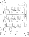
- Fig. 3 depicts an exemplary diagram of the pixel array 22.
- the pixel array 22 is depicted as a 3 x 3 pixel array for explanation purposes, but, the pixel array 22 generally has more than nine pixels.
- the pixel array 22 includes pixels 42, a reset switch 44, and a sensing switch 45.
- Each pixel includes a reset/sense switch 46, an integrating element 48, a read-out amplifier 50, and a read-out switch 52.
- the integrating element 48 integrates charge in response to receiving energy based on x-rays, dark current, and noise, as will be described in more detail below. While we use the term charge in this description, broadly speaking, the charge represents the amount of energy received at the integrating element 48.
- electrons, holes, or other electrical signals that represent the amount of energy received at the integrating element 48.
- Each pixel also receives one of the row select signals 54 and column select signals 56.
- the row select line 54 controls the read-out switch 52.
- the charge stored on each integrating element 48 can be read using the row select signals 54 and column select signals 56 and interpreted to generate an x-ray image 40 as described above.
- the integrating element 48 is erased upon a read out (a "destructive" read). In other embodiments, the integrating element 48 is not erased upon a read out (a "non-destructive" read).
- the pixel array 22 has four general function states: 1) a reset state, 2) a detecting state, 3) an integrating state, and 4) read-out state.
- the reset state the charge stored on the integrating element 48 of each pixel 42 is removed by setting the integrating elements 48 to the reference voltage (e.g., 2 volts).
- the integrating elements 48 are set to the reference voltage by closing the reset/sense switch 46 and the reset switch 44, while leaving the sense switch 45 and read-out switch 52 open.
- the reset/sense switch 46 and the sensing switch 45 are closed to connect integrating elements 48 to sensing line 47, while the reset switch 44 and the read-out switch 52 are left open.
- the pixel array's collective charge is measured to determine whether a threshold has been crossed, which may indicate receipt of x-ray radiation.
- Each integrating element 48 begins with a voltage approximately equal to the reference voltage from the reset state. Thereafter, as charge is integrating at the integrating element 48 from x-ray energy, dark current, and noise, the voltage at the integrating element 48 decreases.
- the collective voltage across the entire pixel array (referred to as the "diode voltage," since the entire pixel array 22 can be viewed as a meta diode) measured across the sense line 47 and ground 59 decreases as the voltage at any integrating element 48 decreases.
- the sense switch 45 only a portion of the pixels 42 are connected to the sense switch 45 during the detecting state.
- additional sense switches 45 are provided in the pixel array 22, and each sense switch 45 is connected to a particular portion of pixels 42. Thus, a particular portion of the pixels 42 may be sensed to have crossed a voltage threshold, as opposed to sensing across the entire pixel array 22.
- the pixel array 22 integrates the charges created by the x-ray radiation as well as by the undesirable noise components (e.g., dark current).
- a signal is provided to a column select line 56 (either j, j + 1, or j + 2).
- a signal is provided along a row select line 54 (either i, i + 1, or i + 2) to a particular row of pixels.
- the read-out switches of the selected row of pixels is closed.
- the charge stored on the integrating elements 48 of the row of pixels is output along the output paths 57.
- the indication provided to the particular column select line 56 serves to chose one of the output paths 57 and allows the charge output along the chosen output path 57 to be input to the A/D converter 58.
- the A/D converter 58 converts the analog signal received from a pixel and outputs a digital signal to the processor 23.
- the A/D converter 58 converts multiple analog signals from pixels 42 to digital signals simultaneously and forwards the digital signals along a multi-bit bus to the processor 23.
- individual pixel A/D converters are provided within each pixel, as opposed to a single A/D converter 58.
- the charge integrating on integrating elements 48 increases (rather than decreases) the voltage stored across each integrating element.
- the reset signal removes the stored charge on each integrating element 48 by causing the voltage across each integrating element 48 to be set to ground.
- the diode voltage increases, rather than decreases, as the pixel array is exposed to x-ray radiation, dark current, and other noise.
- the threshold voltage is set to a value above the reset value and is crossed upon the diode voltage increasing to a level above the threshold.
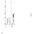
- Fig. 4 depicts a time line 80 for the source 12 emitting an x-ray stream 16, the sensor 20 detecting the x-ray stream, and capturing of the image by the processor 23.
- the pixel array 22 is prepared by repeatedly switching between the reset state and detection state.
- the source 12 begins to emit an x-ray stream 16.
- the sensor 20 detects the x-ray stream 16 and begins integrating charge generated in response to the x-ray stream 16.
- the x-ray radiation emitted from source 12 has concluded.
- the pixel array 22 remains in an integration state.
- the integration time between times 86 and 88 is included to avoid a premature readout that would result in lost x-ray information.
- the charge integrated at the pixel array 22 is read by the processor 23 and, in some embodiments, stored in memory 24.
- the period between times 82 and 84 is in the range of 1 to 6 milliseconds; the period between times 84 and 86 is in the range of 20 to 600 milliseconds; the period between times 86 and 88 is in the range of about 200 hundred milliseconds; and the period between times 88 and the end of the pixel read out is approximately one second.
- the integration period between times 84 and 88 is set to be longer than the length of time the source 12 emits x-ray radiation. In some embodiments, however, the sensor 20 provides circuitry or software to detect the end of x-ray radiation and the read-out operation beginning at time 88 occurs before time 86 and closer to the end of the x-ray radiation.
- the signal received at a pixel of pixel array 22 includes two main portions: a background signal and a signal generated as a result of incident x-ray radiation.
- the background signal is mostly a consequence of 1) dark current, 2) other parameters, and 3) noise.
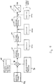
- Fig. 5 shows a model 90 of the x-ray accumulation and the signal output by a single pixel(u,v) of the pixel array 22.
- the charge built up on the pixel includes three components: 1) x-ray signals 92 from source 12, which may have been converted to light by a scintillator or similar device; 2) random noise 94 from various sources, and 3) dark current 96.
- the three components are integrated at the pixel, the function of which is represented at integrator 98.
- the integrator 98 is depicted as integrating element 48 in Fig. 3 .
- the pixel which is a CMOS device in one embodiment, converts the integrated charge into voltage at block 100.
- the block 100 is depicted as read-out amplifier 50 in Fig. 3 .
- a read out of the pixel occurs in steps 104 and 106 by reading out the columns followed by the rows of the pixel array 22. Alternatively, the rows are read out followed a read out of the columns. Regardless of the column-row order, the voltage read out of the pixel array 22 is converted by an A/D converter 108, which may be within the pixel array or outside of the pixel array 22.
- the A/D converter 108 is depicted as A/D converter 58 in Fig. 3 .
- Blocks 102a-c illustrate that the pixel array may also be subject to random noise, but the effect is normally negligible. Gain may be added to the signal either before the A/D 108, within the A/D 108, or digitally after the A/D 108.
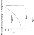
- Fig. 6 shows the influence of temperature on dark current as is known in the semiconductor imaging field.
- the dark current increases. For instance, dark current doubles approximately every 7-11 degrees Celsius.
- the temperature of pixel array 22 can, for instance, increase when placed inside a patient's mouth for an intraoral x-ray, increase when exposed to sunlight, or decrease when exposed to a disinfectant (such as alcohol).
- the dark current if allowed to accumulate, will eventually cause the trigger threshold of the pixel array 22 to be crossed and trigger an image capture when no x-rays have been received.
- Figs. 7 and 8 depict a process 150 of preventing dark current accumulation from falsely triggering pixel array 22 and fixed reset timing diagrams 151a and 151b.
- the process begins at step 152 and proceeds to a reset step 154.
- the reset step 154 the variable "t" is reset to 0 and the pixel array 22 is reset.
- the charge is drained off each pixel as described above with reference to Fig. 3 .
- charge begins to accumulate from sources such as dark current or an x-ray stream 16.
- step 156 the process determines if variable t is equal to a predetermined "reset time.” If the variable t is not equal to the reset time, the process proceeds to step 158.
- step 160 the process returns to step 156 and again determines whether variable t is equal to the reset time. If no x-ray stream 16 is received by pixel array 22 over a predetermined amount of time (reset time), the process steps 156-160 will have repeated enough times such that t will equal reset time in step 156. Processing then proceeds to the reset step 154. and the pixel array 22 is reset such that dark current charge is eliminated from the pixel array 22. The process returns to steps 156-160 to await receipt of an x-ray stream 16. Exemplary reset times may be approximately 1 millisecond. The reset time may be stored in the processor 23 during manufacture of the sensor 20 or at another time before installation of the sensor 20 (installation occurs when the sensor is connected to a user's computer 30). In some embodiments, the reset time is updated in the field to accommodate for different x-ray doses and to account for aging and/or use of the sensor 20.
- step 158 if the charge accumulated in the pixel array 22 exceeds the trigger threshold, the process 150 determines that an x-ray stream 16 has been received by the pixel array 22. Thereafter, in step 162, the pixel array 22 is read by the processor 23 and, in step 164, output to the computer 30.
- Fig. 8 depicts timing diagrams 151a and 151b for the reset signal 181 (sent to pixel array 22 during reset step 154) and the charge accumulation in pixel array 22.
- the diode voltage 182 declines from the initial value.
- the reset signal pulses and the pixel array 22 is reset. If, however, an x-ray stream 16 is received, the diode voltage will drop faster and cross below the threshold voltage 183 and the x-ray stream 16 will be detected (step 158), as shown in timing diagram 151b.
- a reset time of 300 microseconds, threshold voltage 183 of 0.5 V, and initial voltage of 2 V are used. In other embodiments, different values may be used.
- the fixed-timing process 150 of Fig. 7 works in some instances, more adaptive techniques may be employed. If the chosen reset time is too long, dark current will accumulate and trigger an image capture when no x-ray stream has been received. If the chosen reset time is too short, not enough charge will be able to be integrated on the pixel array 22 to signify receipt of x-ray radiation. Thus, the trigger threshold will not be crossed and the x-ray stream 16 will not be detected. Furthermore, the reset time cannot automatically adjust for different environmental settings during operation. For instance, as shown in Fig. 6 , dark current is highly dependent on temperature. The potential for temperature fluctuations increases the difficulty of selecting an appropriate reset time. Additionally, a reset time that is appropriate in a first setting may not be appropriate in a second setting.
- the reset time must be short enough to avoid false triggers by accumulated dark current and long enough to accommodate low doses of x-ray radiation.
- Figs. 9-10 depict an adaptive timing process 250 according to the present invention that address these concerns ( FIG. 10 illustrates a timing diagram 251, which is discussed below).
- the process 250 of Fig. 9 begins at step 252 and proceeds to a reset step 254.
- the variable i is reset to 0 and the pixel array 22 is reset by pulsing the reset signal 256.
- the sensor is allowed to accumulate dark current until the diode voltage 258 crosses the trigger threshold 260 in step 262.
- This value t 0 is the initial dark current trigger time.
- the values of t i are also referred to as a "0"
- the process 250 determines whether the trigger threshold has been crossed by determining if the trigger value 270 has changed to a logic high. Step 268 is repeated until the trigger value 270 is changed to a logic high.
- T AVG represents the average dark current trigger time.
- the average dark current trigger time is the average elapsed time between a reset of the pixel array 22 and the diode voltage crossing the threshold 260 due to dark current.
- T AVG - t i is compared with a multiple of the standard deviation of T AVG . If T AVG - t i is greater than n times the standard deviation of T AVG , an x-ray is detected.
- the comparison of step 278 simply compares the difference of T AVG and t; with a predetermined value (e.g., 0, 1, 2, etc.). If the difference between T AVG and t i is greater than the predetermined value, the method 250 will determine an x-ray has been received at the sensor 20.
- a predetermined value e.g., 0, 1, 2, etc.
- step 276 is replaced by a plurality of sub-steps (not shown), and each sub-step includes a comparison of the difference of T AVG and t i with a unique predetermined value (e.g., 0, 1, 2, etc.) or dynamic value (standard deviation).
- a unique predetermined value e.g., 0, 1, 2, etc.
- dynamic value standard deviation
- a first sub-step for detecting a high-dose rate, short duration exposure may detect an x-ray if the difference of T AVG and t i is greater than X.
- a second sub-step for detecting a low-dose rate, long duration exposure may detect an x-ray if the differences of T AVG and t i , T AVG and t i-1 , T AVG and t i-2 , T AVG and t i-3 , and T AVG and t i-4 are all greater than Y.
- a third sub-step may indicate an x-ray simply by determining that the difference between t i and t i-1 is greater than a variable Z.
- the variable Z should be relatively large such that it is greater than any likely variation caused merely by noise.
- steps 262 and 268 have timeout limits whereby the sensor 20 will produce a timeout signal after a predetermined amount of time if the threshold 260 is not crossed.
- the timeout limits prevent the sensor 20 from waiting an infinite amount of time when an error prevents the threshold 260 from being crossed.
- the T AVG or t i value are used by the processor 23 as an indication that the sensor 20 is over-heated (i.e., from being exposed to direct sunlight). For instance, if T AVG is too low, either in a single instance or over a predetermined number of iterations of dark current causing the diode voltage to cross the threshold 260, the processor 23 concludes that the sensor 20 is over-heated. Appropriate warning signals, alerts, or other information is provided to a user upon detecting that the sensor 20 is over-heated.
- the timing diagram 251 includes trigger value 270, which indicates that the diode voltage 258 has crossed the trigger threshold 260.
- a time is measured by, for instance, counting clock pulses 264.
- the variable t i is then set to the number of clock pulses counted, as described for process 250.
- the reset signal 256 pulses to reset the pixel array 22 and to reset the diode voltage 258.
- a trigger threshold 260 of 0.5 V and initial diode voltage 258 of 2 V are used. In other embodiments, different values are used.
- the senor 20 is configured to be in an armed state or disarmed state.
- the process 250 proceeds normally except that the decision in step 278 is always determined to be false and the process returns to step 266 regardless of the values of T AVG , t i , n, and the standard deviation of T AVG .
- the decision in step 278 is executed normally (if T AVG - t i is greater than the product of the tuning variable n and the standard deviation of T AVG the process proceeds to step 280). However, the values calculated while the sensor 20 was disarmed continue to be used in the armed state
- a constant gain level is applied to the data output from the pixel array 22.
- the gain level alters the rate of change 259 of the diode voltage 258 (see Fig. 10 ). For instance, a higher gain level will increase the rate of change 259 such that less charge integration at the integrating elements 48 is necessary to cause crossing of the threshold voltage 260. A lower gain level, in contrast, will decrease the rate of change 259 such that more charge integration at the integrating elements 48 is necessary to cause crossing of the threshold voltage 260.
- the gain level is altered based on t i levels. For instance, if t i levels are too short, the gain level may be decreased causing the average dark current time to increase.
- the result will include a greater difference between T AVG (average dark current time) and the t i value when an x-ray is received at the sensor. If t; levels are too long, the gain level may be increased such that enough x-ray associated charge is integrated to generate a low noise x-ray image.
- T AVG average dark current time
- the average dark current trigger times calculated in processes 250 are used by the processor 23 to estimate the temperature at which the sensor 20 is operating.
- the calculated temperature can be used, among other reasons, to create temperature records of the sensor 20 and to warn the user that the sensor 20 is operating at a temperature outside of acceptable temperature ranges.
- the temperature records are used to identify thermal stresses placed on the sensor 20 (e.g., stresses caused by spraying the sensor with a disinfectant) or for other maintenance analysis.
- the calculated temperature can be used to scale an offset image of the sensor 20, predict an offset image of the sensor 20, or both.
- a desired integration time for the pixel array 22 is estimated by analyzing the time t i between a reset of the pixel array 22 to the receipt of x-rays at the pixel array 22 (as determined by method 250).
- the time t i is analyzed to estimate the dose rate. The shorter t i , the higher the estimated dose rate because of the reduced amount of time it took for the threshold to be crossed.
- the integration time i.e., the time between times 84 and 88 of Fig. 4
- the integration time i.e., the time between times 84 and 88 of Fig. 4
- the processor 23 estimates a high dose rate, a shorter integration time is used. If the processor 23 estimates a low dose rate, a longer integration time is used. Adjusting the integration time based on an accurately estimated dose rate results in less dark current in the pixel array 22 from long integration times, yet prevents short integration times that cut-off integration of x-ray signals too early.
- the processes 150 and 250 use detection processes based on the cumulative charge across the entire pixel array 22. While measuring the charge on the entire pixel array provides adequate detection in some situations, the level of the cumulative charge integration is altered if the x-ray field does not cover the entire pixel array 22. When the x-ray field does not cover the entire pixel array 22 (also referred to as a "cone cut"), the amount of integration due to x-rays is reduced proportionally to the portion of the pixel array 22 that was not covered, but the effects of dark current are still integrated across the entire pixel array 22. Thus, x-rays may not be detected if the x-ray source is not properly aligned to the pixel array 22. For instance, in Fig.
- the x-ray source 12 is properly aligned and the pixel array 22 is completely within a circle 400 of x-ray stream 16.
- the circle 400 of x-ray stream 16 does not reach the entire pixel array 22. Rather, only a portion of the pixel array 22 receives x-ray radiation. If less than the entire pixel array 22 receives x-ray radiation, a lower amount of charge will be built up on the pixel array 22 than if the entire pixel array was within the circle 400 (as shown, for example, in Fig. 11a ). Thus, in Figs. 11b and 11c , the trigger threshold may not be crossed despite receipt of x-ray radiation.
- the detection processes 150 and 250 monitor multiple sections of the pixel array 22 independently.
- the pixel array 22 of Figs. 11a-c includes 14 sections, four of which are labeled sections 402, 404, 406, and 408 for exemplary purposes.
- the processes will detect an x-ray for the entire pixel array 22 and an image capture will take place.
- the automatic detection processes account for a misaligned x-ray source 12 and sensor 20.
- one or more of the plurality of sections of the pixel array 22 being independently monitored are kept in the detecting mode after detection of x-rays, while the remainder of the pixel array 22 sections are switched to the integration mode.
- the information provided by the few sections that remain in the detecting mode can be used to 1) confirm no false trigger has occurred, 2) detect A/C x-ray pulse patterns, and 3) detect the end of x-ray radiation being received at the pixel array 22.
- detecting the end of x-ray radiation can be used to more closely tailor the duration of integration of the pixel array 22 to the duration of x-ray exposure. More closely tailoring the duration of integration reduces the time period between times 84 and 88 to more closely match the duration of the x-ray exposure.
- the detection processes described above are directed to human dentistry, in some embodiments the processes are used with x-ray sensors intended for: veterinary applications; non-dental applications; and imaging of inanimate objects. Furthermore, in some embodiments, the processor 23 and memory 24 of sensor 20, or their associated functions, reside or are executed within the computer 30.
- the trigger value 270 becomes a logic high upon the diode voltage 258 crossing trigger threshold 260 in Fig. 10 .
- the trigger value 270 becomes a logic low to indicate the trigger threshold 260 has been crossed.
- a source emits x-ray radiation towards an x-ray sensor, and the x-ray sensor automatically detects the x-ray radiation.
- the x-ray sensor automatically detects x-ray radiation by evaluating a time series and determining that a voltage threshold is crossed a certain amount of time earlier than the average time it takes the voltage threshold to be crossed from dark current and other noise.
- the invention provides, among other things, systems and methods for automatic detection of x-rays.
- systems and methods for automatic detection of x-rays are set forth in the following claims.
Landscapes
- Health & Medical Sciences (AREA)
- Life Sciences & Earth Sciences (AREA)
- Engineering & Computer Science (AREA)
- Physics & Mathematics (AREA)
- Medical Informatics (AREA)
- High Energy & Nuclear Physics (AREA)
- Molecular Biology (AREA)
- Multimedia (AREA)
- Signal Processing (AREA)
- General Physics & Mathematics (AREA)
- Biophysics (AREA)
- General Health & Medical Sciences (AREA)
- Veterinary Medicine (AREA)
- Public Health (AREA)
- Animal Behavior & Ethology (AREA)
- Surgery (AREA)
- Heart & Thoracic Surgery (AREA)
- Biomedical Technology (AREA)
- Nuclear Medicine, Radiotherapy & Molecular Imaging (AREA)
- Optics & Photonics (AREA)
- Pathology (AREA)
- Radiology & Medical Imaging (AREA)
- Spectroscopy & Molecular Physics (AREA)
- Dentistry (AREA)
- Oral & Maxillofacial Surgery (AREA)
- Power Engineering (AREA)
- Mathematical Physics (AREA)
- Electromagnetism (AREA)
- Microelectronics & Electronic Packaging (AREA)
- Condensed Matter Physics & Semiconductors (AREA)
- Computer Hardware Design (AREA)
- Apparatus For Radiation Diagnosis (AREA)
Description
- The present invention relates to x-ray imaging. More particularly, embodiments of the invention relate to automatic triggering of an x-ray sensor used in dentistry.
- X-rays have been used in dentistry to image teeth and parts of the mouth for many years. In general, the process involves generating x-rays outside the patient's oral cavity and directing the x-rays at an image receptor located in the patient's mouth. The x-rays are attenuated differently by different parts of the patient's dental structures (e.g., bone versus tissue) and this difference in attenuation is used to create an image, such as on film or by using an electronic image sensor. In most cases, the x-ray source is triggered manually by the operator.
- In other words, the capturing of an image is initiated by a technician or other person by, for example, activating a switch. In the case of film-based systems, the image is captured as soon as the film is exposed to x-ray radiation. So, there is no need to "activate" the film. Once the x-ray source is activated and the x-rays reach the film, an image is captured.
- In electronic systems, the particular image captured depends on at least two factors: activation of the x-ray source and "activation" of the sensor. What constitutes "activation" of the sensor can vary based upon the type of sensor used, but in most cases "activation" occurs when a command is provided to the sensor to either store or output its current image data (referred to herein as "image capture"). So, in some systems, there is an electrical link between the x-ray source and the sensor such that when the x-ray source is activated, a command is sent (simultaneously or nearly simultaneously) to the sensor to perform an image capture. Thus, it is possible to generate a burst of x-ray radiation and be assured that an image will be captured by the sensor during the relatively short period of x-ray exposure.
- Relevant background art includes
U.S. Patent No. 6,404,854 , which discloses an x-ray imaging system. The x-ray imaging system includes an x-ray image sensor having an array of pixels organized in rows and columns and carries out an image capture sequence. The image capture sequence includes a wait for exposure period. During the wait for exposure period the reference pixels are compared with a threshold one by one. If, after a predetermined time interval, a predetermined number of reference pixels are above the threshold, it is decided that exposure has started. - Relevant background art further includes
U.S. Publication No. 2004/065836 , which discloses a method of determining that radiation is incident upon a radiation sensor. The method includes monitoring the magnitude of current drawn by each pixel of a sensor array of an intraoral sensor and generating a signal from the intraoral sensor to a base station, which is connected to a computer. The signal is generated when the amount of current drawn by each pixel exceeds a predetermined amount. - Relevant background art further includes
U.S. Patent No. 5,694,448 , which discloses an imaging apparatus for use in intraoral dental applications. The imaging apparatus includes a charge-coupled device (CCD), which includes an array of radiation sensitive detector elements which accumulate charge depending on the intensity of the radiation directed onto the detector elements. The accumulated charge can be clocked at selected times to produce a signal S. When an x-ray pulse is applied, signal S will rise rapidly. Once the signal S rises above a reference signal, image acquisition begins. - Embodiments of the invention provide automatic triggering of an x-ray sensor. In an automatic x-ray sensor, the sensor detects x-ray radiation from an x-ray source without requiring that a particular trigger signal be sent to the sensor. Although no particular triggering signal is sent to an automatic x-ray sensor, some initializing signals may be sent to the sensor to activate or arm the sensor and indicate it should begin waiting to detect x-ray radiation.
- The inventors have recognized many challenges with respect to automatic triggering systems. One challenge relates to false triggering based on dark current accumulation. As an x-ray sensor waits to detect x-ray radiation from an x-ray source, dark current and other noise can build charge on the sensor and, eventually, cause the sensor to incorrectly determine x-ray radiation has been received. This false triggering issue is amplified as the ambient temperature near the sensor increases because dark current increases with temperature.
- Another challenge associated with automatic triggering systems relates to the alignment between the x-ray source and the sensor. In many instances, even with the use of a positioning system or mechanism, x-ray sensors (particularly those placed in the mouth (i.e., an intra-oral sensor)) are often misaligned. Thus, only a portion of the x-ray sensor is exposed to radiation. In many instances, this partial exposure is not sufficient to cause a simple threshold-based trigger to initiate image capture. Thus, a misalignment may not be recognized until the x-ray technician attempts to review images that he or she believes to have been created only to discover that no such images have been created. The technician may then try to realign the x-ray source and sensor and reinitiate the imaging process. However, it may take several attempts to capture a usable image and each attempt exposes the patient to additional doses of x-ray radiation. As is well-known, high doses of x-ray radiation can have severe adverse effects on an individual's health. So, unnecessary exposure to x-rays should be avoided.
- Yet another challenge associated with automatic triggering systems is the relatively large variation in x-ray doses and dose rates that are provided to perform x-ray image formation in a receptor. The variation in dosages and dose rates is caused by a number of factors including differences in x-ray sources. X-ray sources are manufactured by a number of different manufacturers and their designs and specifications have changed over time. Thus, the intensity of their outputs varies. For example, older x-ray machines usually generate relatively high x-ray doses with alternating dose rates while newer machines generate lower doses with more steady dose rates. The variation in x-ray doses and dose rates received at the sensor is also a consequence of variations in anatomy (from patient to patient) and the distance of the source to the patient. As is known, the dose is dependent on the distance (d) between the source and the patient by a factor of d2.
- The scope of the present invention is set forth in the appended claims. This disclosure provides a method of automatically detecting x-ray radiation with an x-ray sensor. The method includes resetting a pixel array by removing stored charge from the pixel array and measuring, by a processor, an elapsed time since resetting of the pixel array. The method also includes a processor executing a decision operation using the elapsed time and an average dark current trigger time, and determining that a threshold has been crossed. The threshold being crossed indicates a predetermined amount of charge has been stored on at least a portion of the pixel array. The method also includes determining, by the processor, that x-ray radiation has been received at a portion of the pixel array based on the decision operation. Upon determining that x-ray radiation has been received, data is output from the pixel array to be used to generate an x-ray image.
- This disclosure also provides an x-ray sensor that automatically detects receipt of x-rays. The x-ray sensor includes a processor, a pixel array, and a memory. The processor is configured to reset a pixel array by removing stored charge from the pixel array and measure an elapsed time since resetting of the pixel array. The processor is also configured to execute a decision operation using the elapsed time and an average dark current trigger time, and to determine that a threshold has been crossed. The threshold being crossed indicates a predetermined amount of charge has been stored on at least a portion of the pixel array. The processor is configured to determine that x-ray radiation has been received at a portion of the pixel array based on the decision operation. Upon determining that x-ray radiation has been received, the processor is configured to output data from the pixel array to be used to generate an x-ray image.
- Other aspects of the invention will become apparent by consideration of the detailed description and accompanying drawings.
-
-
Fig. 1 illustrates a dental x-ray system including an x-ray source, an intraoral sensor located in a patient's mouth, and a computer connected to the intraoral sensor. -
Fig. 2 illustrates an intraoral sensor. -
Fig. 3 illustrates a circuit diagram of a pixel array according to some embodiments of the invention. -
Fig. 4 depicts a timing diagram of x-ray exposure on a pixel array. -
Fig. 5 depicts a flow chart of x-ray accumulation and output by a pixel. -
Fig. 6 depicts a graph of dark current relative to temperature. -
Fig. 7 illustrates a process of automatically detecting x-ray radiation. -
Fig. 8 illustrates fixed reset timing diagrams. -
Fig. 9 illustrates a process of automatically detecting x-ray radiation. -
Fig. 10 illustrates a fully adaptive reset timing diagram. -
Figs. 11a-c illustrate a sensor receiving x-ray radiation. - Before any embodiments of the invention are explained in detail, it is to be understood that the invention is not limited in its application to the details of construction and the arrangement of components set forth in the following description or illustrated in the following drawings. The invention is capable of other embodiments and of being practiced or of being carried out in various ways. Additionally, the term processor as is used in this application to mean any of a microcontroller, programmable logic device (e.g., a field programmable gate array "FPGA"), a general purpose processor, specifically designed hardware (e.g., an application specific integrated circuit "ASIC"), or a combination thereof.
-
Fig. 1 illustrates adental x-ray system 10. The system includes anx-ray source 12. In the embodiment shown, the source is located on anend 13 of amechanical arm 15. When activated, thex-ray source 12 generates anx-ray stream 16. (Of course, x-rays are generally invisible, but a representation of a stream is illustrated to facilitate understanding of the invention.) In some applications, a removable collimator is used with a mechanical positioning device to help align the x-ray stream with an x-ray sensor. - As shown in
Fig. 1 , thearm 15 is positioned (e.g., by an operator) so that the x-ray stream is directed to anintraoral sensor 20. Theintraoral sensor 20 is shown located in the mouth of a patient 21. In some embodiments, theintraoral sensor 20 includes a scintillator that coverts x-ray radiation to visible light and light detecting elements that convert the visible light to electrons. In other embodiments, thesensor 20 is configured to convert x-rays to electrons without a scintillator. - As best seen by reference to
Fig. 2 , thesensor 20 also includes an array ofpixels 22. Each pixel produces an electric signal in response to light (from the scintillator) or x-ray radiation impinged upon it. In one embodiment, thesensor 20 includes one or more analog-to-digital ("A/D") converters to covert analog signals generated by the pixels to digital signals. These signals are provided to a processor 23 (such as a programmable, electronic microprocessor, FPGA, ASIC, or similar device). In some embodiments, the A/D converters are implemented as part of thepixel array 22, as part of theprocessor 23, or as separate components between thepixel array 22 and theprocessor 23. In the embodiment shown, theprocessor 23 is connected to memory 24 (ROM and RAM) and an input-output interface 25. Thesensor 20 also includes one or more electronic circuits for power supply, driving the pixel array, and driving the output (e.g., circuits located in the I/O interface 25). To facilitate the illustration of the connections betweenpixel array 22 andcomponents array 22 is shown as covering only a portion of thesensor 20. However, in most applications, thearray 22 is generally coextensive with thesensor 20 and thecomponents array 22, rather than to the side of the array 22 (as shown inFig. 2 ). - Referring back to
Fig. 1 , a wire, cable, or similar connecter 27 of thesensor 20 connects thesensor 20 to acomputer 30. Thecomputer 30 includes various components, including a processor or similarelectronic device 32, an input/output interface 34, and memory 36 (e.g., RAM and ROM). In one particular embodiment, the input/output interface 34 is a Universal Serial Bus ("USB") connection and the connector 27 is a USB cable. In other embodiments, a wireless connection is made between thesensor 20 andcomputer 30.Fig. 1 illustrates that image data captured by thesensor 20 and processed by thecomputer 30 is sent to adisplay 38 and viewed asimage 40. (Image 40 is drawn more distinctly than an x-ray image would typically appear.) -
Fig. 3 depicts an exemplary diagram of thepixel array 22. Thepixel array 22 is depicted as a 3 x 3 pixel array for explanation purposes, but, thepixel array 22 generally has more than nine pixels. Thepixel array 22 includespixels 42, areset switch 44, and asensing switch 45. Each pixel includes a reset/sense switch 46, an integratingelement 48, a read-out amplifier 50, and a read-out switch 52. The integratingelement 48 integrates charge in response to receiving energy based on x-rays, dark current, and noise, as will be described in more detail below. While we use the term charge in this description, broadly speaking, the charge represents the amount of energy received at the integratingelement 48. In other embodiments, electrons, holes, or other electrical signals, whether analog or digital, that represent the amount of energy received at the integratingelement 48. Each pixel also receives one of the rowselect signals 54 and column select signals 56. The rowselect line 54 controls the read-out switch 52. The charge stored on each integratingelement 48 can be read using the rowselect signals 54 and columnselect signals 56 and interpreted to generate anx-ray image 40 as described above. In some embodiments, the integratingelement 48 is erased upon a read out (a "destructive" read). In other embodiments, the integratingelement 48 is not erased upon a read out (a "non-destructive" read). - The
pixel array 22 has four general function states: 1) a reset state, 2) a detecting state, 3) an integrating state, and 4) read-out state. In the reset state, the charge stored on the integratingelement 48 of eachpixel 42 is removed by setting the integratingelements 48 to the reference voltage (e.g., 2 volts). The integratingelements 48 are set to the reference voltage by closing the reset/sense switch 46 and thereset switch 44, while leaving thesense switch 45 and read-out switch 52 open. - In the detecting state, the reset/
sense switch 46 and thesensing switch 45 are closed to connect integratingelements 48 to sensingline 47, while thereset switch 44 and the read-out switch 52 are left open. In the detecting state, the pixel array's collective charge is measured to determine whether a threshold has been crossed, which may indicate receipt of x-ray radiation. Each integratingelement 48 begins with a voltage approximately equal to the reference voltage from the reset state. Thereafter, as charge is integrating at the integratingelement 48 from x-ray energy, dark current, and noise, the voltage at the integratingelement 48 decreases. Therefore, the collective voltage across the entire pixel array (referred to as the "diode voltage," since theentire pixel array 22 can be viewed as a meta diode) measured across thesense line 47 andground 59 decreases as the voltage at any integratingelement 48 decreases. In some embodiments, only a portion of thepixels 42 are connected to thesense switch 45 during the detecting state. In other embodiments, additional sense switches 45 are provided in thepixel array 22, and eachsense switch 45 is connected to a particular portion ofpixels 42. Thus, a particular portion of thepixels 42 may be sensed to have crossed a voltage threshold, as opposed to sensing across theentire pixel array 22. - In the integration state, all switches (44, 45, 46, and 52) are open. The
pixel array 22 integrates the charges created by the x-ray radiation as well as by the undesirable noise components (e.g., dark current). - In the read-out state, a signal is provided to a column select line 56 (either j, j + 1, or j + 2). In addition, a signal is provided along a row select line 54 (either i, i + 1, or i + 2) to a particular row of pixels. In response, the read-out switches of the selected row of pixels is closed. The charge stored on the integrating
elements 48 of the row of pixels is output along theoutput paths 57. The indication provided to the particular columnselect line 56 serves to chose one of theoutput paths 57 and allows the charge output along the chosenoutput path 57 to be input to the A/D converter 58. The A/D converter 58 converts the analog signal received from a pixel and outputs a digital signal to theprocessor 23. By repeating this process for eachpixel 42 through providing signals to the appropriate rowselect line 54 and columnselect line 56, theentire pixel array 22 is read out. - In some embodiments, multiple pixels are read out in parallel. For instance, in some embodiments, the A/D converter 58 converts multiple analog signals from
pixels 42 to digital signals simultaneously and forwards the digital signals along a multi-bit bus to theprocessor 23. In other embodiments, individual pixel A/D converters are provided within each pixel, as opposed to a single A/D converter 58. In some embodiments, the charge integrating on integratingelements 48 increases (rather than decreases) the voltage stored across each integrating element. In this embodiment, the reset signal removes the stored charge on each integratingelement 48 by causing the voltage across each integratingelement 48 to be set to ground. Additionally, the diode voltage increases, rather than decreases, as the pixel array is exposed to x-ray radiation, dark current, and other noise. Thus, the threshold voltage is set to a value above the reset value and is crossed upon the diode voltage increasing to a level above the threshold. -
Fig. 4 depicts atime line 80 for thesource 12 emitting anx-ray stream 16, thesensor 20 detecting the x-ray stream, and capturing of the image by theprocessor 23. Before time 82, thepixel array 22 is prepared by repeatedly switching between the reset state and detection state. At time 82, thesource 12 begins to emit anx-ray stream 16. At time 84, thesensor 20 detects thex-ray stream 16 and begins integrating charge generated in response to thex-ray stream 16. At time 86, the x-ray radiation emitted fromsource 12 has concluded. Betweentimes 86 and 88, thepixel array 22 remains in an integration state. In some embodiments, the integration time betweentimes 86 and 88 is included to avoid a premature readout that would result in lost x-ray information. Attime 88, the charge integrated at thepixel array 22 is read by theprocessor 23 and, in some embodiments, stored in memory 24. In one embodiment, the period between times 82 and 84 is in the range of 1 to 6 milliseconds; the period between times 84 and 86 is in the range of 20 to 600 milliseconds; the period betweentimes 86 and 88 is in the range of about 200 hundred milliseconds; and the period betweentimes 88 and the end of the pixel read out is approximately one second. Generally, the integration period betweentimes 84 and 88 is set to be longer than the length of time thesource 12 emits x-ray radiation. In some embodiments, however, thesensor 20 provides circuitry or software to detect the end of x-ray radiation and the read-out operation beginning attime 88 occurs before time 86 and closer to the end of the x-ray radiation. - The signal received at a pixel of
pixel array 22 includes two main portions: a background signal and a signal generated as a result of incident x-ray radiation. The background signal is mostly a consequence of 1) dark current, 2) other parameters, and 3) noise. When the sum of the signals on thepixel array 22 cross a trigger threshold level, thesensor 20 detects an x-ray or performs additional steps to determine whether an x-ray has been received, as will be described below. -
Fig. 5 shows a model 90 of the x-ray accumulation and the signal output by a single pixel(u,v) of thepixel array 22. The charge built up on the pixel includes three components: 1) x-ray signals 92 fromsource 12, which may have been converted to light by a scintillator or similar device; 2)random noise 94 from various sources, and 3) dark current 96. The three components are integrated at the pixel, the function of which is represented atintegrator 98. Theintegrator 98 is depicted as integratingelement 48 inFig. 3 . The pixel, which is a CMOS device in one embodiment, converts the integrated charge into voltage atblock 100. Theblock 100 is depicted as read-out amplifier 50 inFig. 3 . Thereafter, a read out of the pixel occurs insteps pixel array 22. Alternatively, the rows are read out followed a read out of the columns. Regardless of the column-row order, the voltage read out of thepixel array 22 is converted by an A/D converter 108, which may be within the pixel array or outside of thepixel array 22. The A/D converter 108 is depicted as A/D converter 58 inFig. 3 . Blocks 102a-c illustrate that the pixel array may also be subject to random noise, but the effect is normally negligible. Gain may be added to the signal either before the A/D 108, within the A/D 108, or digitally after the A/D 108. -
Fig. 6 shows the influence of temperature on dark current as is known in the semiconductor imaging field. As the temperature of thepixel array 22 ofsensor 20 increases (either on a particular portion or globally), the dark current increases. For instance, dark current doubles approximately every 7-11 degrees Celsius. The temperature ofpixel array 22 can, for instance, increase when placed inside a patient's mouth for an intraoral x-ray, increase when exposed to sunlight, or decrease when exposed to a disinfectant (such as alcohol). The dark current, if allowed to accumulate, will eventually cause the trigger threshold of thepixel array 22 to be crossed and trigger an image capture when no x-rays have been received. -
Figs. 7 and8 depict aprocess 150 of preventing dark current accumulation from falsely triggeringpixel array 22 and fixed reset timing diagrams 151a and 151b. The process begins atstep 152 and proceeds to areset step 154. In thereset step 154, the variable "t" is reset to 0 and thepixel array 22 is reset. To reset thepixel array 22, the charge is drained off each pixel as described above with reference toFig. 3 . After the reset, charge begins to accumulate from sources such as dark current or anx-ray stream 16. Instep 156, the process determines if variable t is equal to a predetermined "reset time." If the variable t is not equal to the reset time, the process proceeds to step 158. Instep 158, the process determines whether charge accumulated in thepixel array 22 has exceeded the trigger threshold. If not, the process proceeds to step 160, where variable t is increased by one (i.e., t = t + 1). - After
step 160, the process returns to step 156 and again determines whether variable t is equal to the reset time. If nox-ray stream 16 is received bypixel array 22 over a predetermined amount of time (reset time), the process steps 156-160 will have repeated enough times such that t will equal reset time instep 156. Processing then proceeds to thereset step 154. and thepixel array 22 is reset such that dark current charge is eliminated from thepixel array 22. The process returns to steps 156-160 to await receipt of anx-ray stream 16. Exemplary reset times may be approximately 1 millisecond. The reset time may be stored in theprocessor 23 during manufacture of thesensor 20 or at another time before installation of the sensor 20 (installation occurs when the sensor is connected to a user's computer 30). In some embodiments, the reset time is updated in the field to accommodate for different x-ray doses and to account for aging and/or use of thesensor 20. - In
step 158, if the charge accumulated in thepixel array 22 exceeds the trigger threshold, theprocess 150 determines that anx-ray stream 16 has been received by thepixel array 22. Thereafter, instep 162, thepixel array 22 is read by theprocessor 23 and, instep 164, output to thecomputer 30. -
Fig. 8 depicts timing diagrams 151a and 151b for the reset signal 181 (sent topixel array 22 during reset step 154) and the charge accumulation inpixel array 22. As charge accumulates in thepixel array 22, thediode voltage 182 declines from the initial value. As shown in timing diagram 151a, after the reset time passes (t = reset time in step 156), assuming nox-ray stream 16 has been received by the pixel array, the reset signal pulses and thepixel array 22 is reset. If, however, anx-ray stream 16 is received, the diode voltage will drop faster and cross below thethreshold voltage 183 and thex-ray stream 16 will be detected (step 158), as shown in timing diagram 151b. In the embodiment shown inFig. 8 , a reset time of 300 microseconds,threshold voltage 183 of 0.5 V, and initial voltage of 2 V are used. In other embodiments, different values may be used. - Although the fixed-
timing process 150 ofFig. 7 works in some instances, more adaptive techniques may be employed. If the chosen reset time is too long, dark current will accumulate and trigger an image capture when no x-ray stream has been received. If the chosen reset time is too short, not enough charge will be able to be integrated on thepixel array 22 to signify receipt of x-ray radiation. Thus, the trigger threshold will not be crossed and thex-ray stream 16 will not be detected. Furthermore, the reset time cannot automatically adjust for different environmental settings during operation. For instance, as shown inFig. 6 , dark current is highly dependent on temperature. The potential for temperature fluctuations increases the difficulty of selecting an appropriate reset time. Additionally, a reset time that is appropriate in a first setting may not be appropriate in a second setting. One additional issue is that different amounts of radiation may be emitted depending on thesource 12, the distance between thesource 12 andsensor 20, the alignment of thesource 12 andsensor 20. As such, the reset time must be short enough to avoid false triggers by accumulated dark current and long enough to accommodate low doses of x-ray radiation. -
Figs. 9-10 depict anadaptive timing process 250 according to the present invention that address these concerns (Fig. 10 illustrates a timing diagram 251, which is discussed below). Theprocess 250 ofFig. 9 begins atstep 252 and proceeds to areset step 254. Inreset step 254, the variable i is reset to 0 and thepixel array 22 is reset by pulsing thereset signal 256. After the reset step, the sensor is allowed to accumulate dark current until thediode voltage 258 crosses thetrigger threshold 260 instep 262. A counter counts the number ofclock pulses 264 between thereset step 254 and the dark current causing thetrigger threshold 260 to be crossed and sets t0 = number ofclock pulses 264. This value t0 is the initial dark current trigger time. The values of ti are also referred to as a "time series." - The
process 250 proceeds to step 266, where the pixel array is again reset and i = i + 1 by pulsingreset signal 256. Instep 268, theprocess 250 determines whether the trigger threshold has been crossed by determining if thetrigger value 270 has changed to a logic high. Step 268 is repeated until thetrigger value 270 is changed to a logic high. Upon thetrigger value 270 becoming a logic high,step 272 sets ti = the number ofclock pulses 264 that have elapsed since thereset step 266. Instep 276, TAVG (the running average of ti from i = 0 to i) is calculated. Additionally, the standard deviation of TAVG from time i = 0 to i is calculated instep 276. TAVG represents the average dark current trigger time. The average dark current trigger time is the average elapsed time between a reset of thepixel array 22 and the diode voltage crossing thethreshold 260 due to dark current. In some embodiments, TAVG is simply set equal to ti-1 or is the running average of t; for only maximum number of previous ti values (e.g., ti from i = i-20 to i). - Thereafter, in
step 278, TAVG- ti is compared with a multiple of the standard deviation of TAVG. If TAVG - ti is greater than n times the standard deviation of TAVG, an x-ray is detected. The value of fine tuning variable "n" is selected to adjust the detection process. In some embodiments, 0 < n < 1, meaning that small variations from the TAVG will result in an x-ray detection. In other embodiments, n > 1, and only large variations from TAVG will result in an x-ray detection. In still other embodiments, n = 1, and any variation from TAVG greater than the standard deviation will result in an x-ray detection. Upon detection of an x-ray, theprocess 250 proceeds to step 280, where thepixel array 22 is read by theprocessor 23 and, instep 282, output to thecomputer 30. If instep 278, however, ti - TAVG is less than the product of n and the standard deviation of TAVG, the process returns to step 266 to reset the pixel array and sets i = i + 1. - In some embodiments, the comparison of
step 278 simply compares the difference of TAVG and t; with a predetermined value (e.g., 0, 1, 2, etc.). If the difference between TAVG and ti is greater than the predetermined value, themethod 250 will determine an x-ray has been received at thesensor 20. - In other embodiments,
step 276 is replaced by a plurality of sub-steps (not shown), and each sub-step includes a comparison of the difference of TAVG and ti with a unique predetermined value (e.g., 0, 1, 2, etc.) or dynamic value (standard deviation). Using the plurality of comparisons enables theprocess 250 to detect both 1) high-dose rate, short duration x-ray exposures and 2) low-dose rate, long duration x-ray exposures. To detect high-dose rate, short duration exposures, one sub-step may include a detection algorithm that focuses only on the most recent ti values. To detect low-dose rate, long duration exposures, another sub-step may include a detection algorithm that analyzes ti values over a longer period of time. The sub-steps are executed in parallel and, if any sub-step indicates that an x-ray is detected, theprocess 250 proceeds to step 280. For instance, where variable X is greater than variable Y, a first sub-step for detecting a high-dose rate, short duration exposure, may detect an x-ray if the difference of TAVG and ti is greater than X. A second sub-step for detecting a low-dose rate, long duration exposure, may detect an x-ray if the differences of TAVG and ti, TAVG and ti-1, TAVG and ti-2, TAVG and ti-3, and TAVG and ti-4 are all greater than Y. X and Y may be predetermined static values or may be based in part on dynamic values such as the standard deviations of TAVG, but using different fine tuning variables n. A third sub-step may indicate an x-ray simply by determining that the difference between ti and ti-1 is greater than a variable Z. In this third sub-step, the variable Z should be relatively large such that it is greater than any likely variation caused merely by noise. - In some embodiments,
steps sensor 20 will produce a timeout signal after a predetermined amount of time if thethreshold 260 is not crossed. Thus, the timeout limits prevent thesensor 20 from waiting an infinite amount of time when an error prevents thethreshold 260 from being crossed. - In some embodiments, the TAVG or ti value are used by the
processor 23 as an indication that thesensor 20 is over-heated (i.e., from being exposed to direct sunlight). For instance, if TAVG is too low, either in a single instance or over a predetermined number of iterations of dark current causing the diode voltage to cross thethreshold 260, theprocessor 23 concludes that thesensor 20 is over-heated. Appropriate warning signals, alerts, or other information is provided to a user upon detecting that thesensor 20 is over-heated. - Referring now to
Fig. 10 , the timing diagram 251 includestrigger value 270, which indicates that thediode voltage 258 has crossed thetrigger threshold 260. A time is measured by, for instance, countingclock pulses 264. The variable ti is then set to the number of clock pulses counted, as described forprocess 250. Thereset signal 256 pulses to reset thepixel array 22 and to reset thediode voltage 258. In the embodiment shown inFig. 10 , atrigger threshold 260 of 0.5 V andinitial diode voltage 258 of 2 V are used. In other embodiments, different values are used. - In some embodiments of
process 250, thesensor 20 is configured to be in an armed state or disarmed state. When thesensor 20 is in a disarmed state, theprocess 250 proceeds normally except that the decision instep 278 is always determined to be false and the process returns to step 266 regardless of the values of TAVG, ti, n, and the standard deviation of TAVG. Whensensor 20 is armed, the decision instep 278 is executed normally (if TAVG- ti is greater than the product of the tuning variable n and the standard deviation of TAVG the process proceeds to step 280). However, the values calculated while thesensor 20 was disarmed continue to be used in the armed state - In some embodiments, a constant gain level is applied to the data output from the
pixel array 22. The gain level alters the rate of change 259 of the diode voltage 258 (seeFig. 10 ). For instance, a higher gain level will increase the rate of change 259 such that less charge integration at the integratingelements 48 is necessary to cause crossing of thethreshold voltage 260. A lower gain level, in contrast, will decrease the rate of change 259 such that more charge integration at the integratingelements 48 is necessary to cause crossing of thethreshold voltage 260. In some embodiments, the gain level is altered based on ti levels. For instance, if ti levels are too short, the gain level may be decreased causing the average dark current time to increase. Generally, the result will include a greater difference between TAVG (average dark current time) and the ti value when an x-ray is received at the sensor. If t; levels are too long, the gain level may be increased such that enough x-ray associated charge is integrated to generate a low noise x-ray image. - In some embodiments, the average dark current trigger times calculated in
processes 250 are used by theprocessor 23 to estimate the temperature at which thesensor 20 is operating. The calculated temperature can be used, among other reasons, to create temperature records of thesensor 20 and to warn the user that thesensor 20 is operating at a temperature outside of acceptable temperature ranges. The temperature records are used to identify thermal stresses placed on the sensor 20 (e.g., stresses caused by spraying the sensor with a disinfectant) or for other maintenance analysis. Furthermore, the calculated temperature can be used to scale an offset image of thesensor 20, predict an offset image of thesensor 20, or both. - In other embodiments, a desired integration time for the
pixel array 22 is estimated by analyzing the time ti between a reset of thepixel array 22 to the receipt of x-rays at the pixel array 22 (as determined by method 250). The time ti is analyzed to estimate the dose rate. The shorter ti, the higher the estimated dose rate because of the reduced amount of time it took for the threshold to be crossed. Once an estimated dose rate is determined, the integration time (i.e., the time betweentimes 84 and 88 ofFig. 4 ) can be properly adjusted. For example, if theprocessor 23 estimates a high dose rate, a shorter integration time is used. If theprocessor 23 estimates a low dose rate, a longer integration time is used. Adjusting the integration time based on an accurately estimated dose rate results in less dark current in thepixel array 22 from long integration times, yet prevents short integration times that cut-off integration of x-ray signals too early. - The
processes entire pixel array 22. While measuring the charge on the entire pixel array provides adequate detection in some situations, the level of the cumulative charge integration is altered if the x-ray field does not cover theentire pixel array 22. When the x-ray field does not cover the entire pixel array 22 (also referred to as a "cone cut"), the amount of integration due to x-rays is reduced proportionally to the portion of thepixel array 22 that was not covered, but the effects of dark current are still integrated across theentire pixel array 22. Thus, x-rays may not be detected if the x-ray source is not properly aligned to thepixel array 22. For instance, inFig. 11a , thex-ray source 12 is properly aligned and thepixel array 22 is completely within a circle 400 ofx-ray stream 16. InFigs. 11b and 11c , however, the circle 400 ofx-ray stream 16 does not reach theentire pixel array 22. Rather, only a portion of thepixel array 22 receives x-ray radiation. If less than theentire pixel array 22 receives x-ray radiation, a lower amount of charge will be built up on thepixel array 22 than if the entire pixel array was within the circle 400 (as shown, for example, inFig. 11a ). Thus, inFigs. 11b and 11c , the trigger threshold may not be crossed despite receipt of x-ray radiation. - In some embodiments, to account for misaligned x-ray sources, the detection processes 150 and 250 monitor multiple sections of the
pixel array 22 independently. For instance, thepixel array 22 ofFigs. 11a-c includes 14 sections, four of which are labeledsections 402, 404, 406, and 408 for exemplary purposes. Thus, if an x-ray is detected on any of the sections, the processes will detect an x-ray for theentire pixel array 22 and an image capture will take place. Thus, the automatic detection processes account for amisaligned x-ray source 12 andsensor 20. - In some embodiments, one or more of the plurality of sections of the
pixel array 22 being independently monitored are kept in the detecting mode after detection of x-rays, while the remainder of thepixel array 22 sections are switched to the integration mode. The information provided by the few sections that remain in the detecting mode can be used to 1) confirm no false trigger has occurred, 2) detect A/C x-ray pulse patterns, and 3) detect the end of x-ray radiation being received at thepixel array 22. As discussed above, detecting the end of x-ray radiation can be used to more closely tailor the duration of integration of thepixel array 22 to the duration of x-ray exposure. More closely tailoring the duration of integration reduces the time period betweentimes 84 and 88 to more closely match the duration of the x-ray exposure. - Although the detection processes described above are directed to human dentistry, in some embodiments the processes are used with x-ray sensors intended for: veterinary applications; non-dental applications; and imaging of inanimate objects. Furthermore, in some embodiments, the
processor 23 and memory 24 ofsensor 20, or their associated functions, reside or are executed within thecomputer 30. - Although the timing diagrams and processes were described with particular logic states, e.g., logic high and logic low, embodiments of the invention contemplate using alternative signal orientations to signal similar events. For instance, the
trigger value 270 becomes a logic high upon thediode voltage 258crossing trigger threshold 260 inFig. 10 . However, in some embodiments, thetrigger value 270 becomes a logic low to indicate thetrigger threshold 260 has been crossed. - There has been described a system and method for automatic detection of x-rays at an x-ray sensor. A source emits x-ray radiation towards an x-ray sensor, and the x-ray sensor automatically detects the x-ray radiation. The x-ray sensor automatically detects x-ray radiation by evaluating a time series and determining that a voltage threshold is crossed a certain amount of time earlier than the average time it takes the voltage threshold to be crossed from dark current and other noise.
- Thus, the invention provides, among other things, systems and methods for automatic detection of x-rays. Various features and advantages of the invention are set forth in the following claims.
Claims (11)
- A method of automatically detecting x-ray radiation with an x-ray sensor, the method comprising:resetting a pixel array by removing stored charge from the pixel array (254,266);determining an average dark current trigger time (262);measuring an elapsed time since resetting of the pixel array (272);performing a comparison based upon the elapsed time and the average dark current trigger time (276);determining that a threshold has been crossed, crossing of the threshold indicating that a predetermined amount of charge has been stored on at least a portion of the pixel array (268);determining that x-ray radiation has been received at the at least a portion of the pixel array based on the comparison (278); andupon determining that x-ray radiation has been received (278), outputting data from the pixel array (280, 282) to be used to generate an x-ray image;wherein the average dark current trigger time is based on iteratively calculating the elapsed time between resetting of the pixel array and the determination that the threshold has been crossed due to dark current.
- The method of claim 1, wherein performing a comparison includes comparing a difference between the elapsed time and the average dark current trigger time with at least one ofa predetermined value, anda product of a fine tuning variable and a standard deviation of the average dark current trigger time.
- The method of claim 2, wherein x-ray radiation is determined to have been received at the at least a portion of the pixel array if the difference is greater than the at least one of the predetermined value or the standard deviation.
- The method of any one of the preceding claims, wherein the average dark current trigger time indicates a temperature of the x-ray sensor.
- The method of claim 4, further comprising generating an error condition if the temperature of the x-ray sensor indicated by the average dark current trigger time exceeds a predetermined level.
- The method of any one of the preceding claims, wherein the threshold is a predetermined voltage level, and wherein the predetermined amount of charge stored on the at least a portion of the pixel array causes a voltage potential at a diode to drop below the threshold.
- The method of any one of the preceding claims, further comprisingperforming a second comparison based on using the elapsed time and the average dark current trigger time,wherein said performing a comparison includes comparing a difference between the elapsed time and the average dark current trigger time with a first value,and wherein said performing a second comparison includes comparing the difference with a second value and comparing a second difference between a previous elapsed time and a previous average dark current trigger time with the second value.
- The method of claim 7, wherein x-ray radiation is determined to have been received at the at least a portion of the pixel array ifthe difference is greater than the first value, orboth the difference and the second difference are greater than the second value.
- The method of claim 8, further comprising concluding 1) a high dose rate occurred if the difference is greater than the first value and 2) a low dose rate occurred if both the difference and the second difference are greater than the second value, wherein the first value is greater than the second value.
- The method of any one of the preceding claims, further comprisingdetermining that the x-ray radiation is no longer being received, andreducing an integration time for a subsequent x-ray radiation exposure based on a duration of the x-ray radiation received at the at least a portion of the pixel array.
- An x-ray sensor that automatically detects receipt of x-rays, the x-ray sensor including a processor, a pixel array, and a memory, the processor configured to implement a method in accordance with any one of the preceding claims.
Applications Claiming Priority (1)
| Application Number | Priority Date | Filing Date | Title |
|---|---|---|---|
| US10855208P | 2008-10-27 | 2008-10-27 |
Publications (3)
| Publication Number | Publication Date |
|---|---|
| EP2180343A2 EP2180343A2 (en) | 2010-04-28 |
| EP2180343A3 EP2180343A3 (en) | 2013-05-29 |
| EP2180343B1 true EP2180343B1 (en) | 2018-07-25 |
Family
ID=42016980
Family Applications (1)
| Application Number | Title | Priority Date | Filing Date |
|---|---|---|---|
| EP09174091.0A Active EP2180343B1 (en) | 2008-10-27 | 2009-10-26 | System and method of x-ray detection with a sensor |
Country Status (5)
| Country | Link |
|---|---|
| US (3) | US8119990B2 (en) |
| EP (1) | EP2180343B1 (en) |
| JP (1) | JP5769921B2 (en) |
| KR (1) | KR101719814B1 (en) |
| IL (1) | IL201765A (en) |
Families Citing this family (36)
| Publication number | Priority date | Publication date | Assignee | Title |
|---|---|---|---|---|
| US9492129B2 (en) * | 2008-10-27 | 2016-11-15 | Dental Imaging Technologies Corporation | Triggering of intraoral X-ray sensor using pixel array sub-sampling |
| US8366318B2 (en) | 2009-07-17 | 2013-02-05 | Dental Imaging Technologies Corporation | Intraoral X-ray sensor with embedded standard computer interface |
| JP5464064B2 (en) * | 2010-06-09 | 2014-04-09 | コニカミノルタ株式会社 | Portable radiographic imaging device and radiographic imaging system |
| JP5475574B2 (en) * | 2010-07-02 | 2014-04-16 | 富士フイルム株式会社 | Radiation detection element and radiographic imaging device |
| JP2012083307A (en) * | 2010-10-14 | 2012-04-26 | Fujifilm Corp | Radiation detection device, radiation image photographing system, radiation detection program and radiation detection method |
| JP5209021B2 (en) | 2010-10-19 | 2013-06-12 | 富士フイルム株式会社 | Radiation image capturing apparatus, radiation image capturing system, radiation image capturing program, and radiation image capturing method |
| JP5289477B2 (en) * | 2011-02-09 | 2013-09-11 | 富士フイルム株式会社 | Radiation image detection apparatus and radiation irradiation start detection method |
| US8729485B2 (en) | 2012-02-17 | 2014-05-20 | Luxen Technologies, Inc. | Parallel mode readout integrated circuit for X-ray image sensor |
| US20130256542A1 (en) | 2012-03-28 | 2013-10-03 | Luxen Technologies, Inc. | Programmable readout integrated circuit for an ionizing radiation sensor |
| US9128195B2 (en) | 2012-03-28 | 2015-09-08 | Luxen Technologies, Inc. | Increasing dynamic range for x-ray image sensor |
| US8942444B2 (en) | 2012-08-17 | 2015-01-27 | General Electric Company | System and method for image compression in X-ray imaging systems |
| KR101389525B1 (en) * | 2012-12-20 | 2014-04-25 | 아스텔 주식회사 | X-ray detector apparatus, x-ray image taking system using the x-ray detector apparatus |
| US9113827B2 (en) * | 2013-01-17 | 2015-08-25 | Jordan C. Christoff | Intraoral X-ray imaging device with optimized image data output |
| US9788809B2 (en) * | 2013-03-06 | 2017-10-17 | Canon Kabushiki Kaisha | Apparatus, method and computer-readable medium storing program for radiographic imaging with elapsed time control of radiation sensor apparatus |
| KR102025928B1 (en) * | 2013-05-14 | 2019-09-26 | 삼성전자주식회사 | Imaging apparatus and controlling method thereof |
| KR102208106B1 (en) * | 2014-04-03 | 2021-01-28 | 주식회사 레이언스 | Imaging system including image sensor and method of driving the same |
| JP6491432B2 (en) * | 2014-08-08 | 2019-03-27 | キヤノン株式会社 | Radiation imaging apparatus and control method thereof |
| FR3025086B1 (en) * | 2014-09-02 | 2016-11-11 | E2V Semiconductors | METHOD AND SYSTEM FOR TAKING MEDICAL RADIOLOGICAL IMAGES WITH STOP CONTROL OF THE X-RAY SOURCE |
| KR20160048538A (en) | 2014-10-24 | 2016-05-04 | 삼성전자주식회사 | Apparatus and method for detecting X-ray, X-ray imaging system |
| KR101687522B1 (en) | 2015-06-25 | 2016-12-20 | 주식회사 뷰웍스 | X-ray detector |
| CN105496444B (en) * | 2015-12-01 | 2018-06-26 | 苏州佳世达光电有限公司 | Scan control method and scanning means |
| FR3046679B1 (en) | 2016-01-12 | 2019-12-27 | Teledyne E2V Semiconductors Sas | X-RAY DETECTION CIRCUIT FOR DENTAL RADIOLOGICAL SENSOR |
| US10213180B2 (en) * | 2016-09-14 | 2019-02-26 | Dental Imaging Technologies Corporation | Multiple-dimension imaging sensor with operation based on magnetic field detection |
| US10932733B2 (en) | 2016-09-14 | 2021-03-02 | Dental Imaging Technologies Corporation | Multiple-dimension imaging sensor with operation based on movement detection |
| US10299741B2 (en) * | 2016-09-14 | 2019-05-28 | Dental Imaging Technologies Corporation | Multiple-dimension imaging sensor and state-based operation of an imaging system including a multiple-dimension imaging sensor |
| US10299742B2 (en) * | 2016-09-14 | 2019-05-28 | Dental Imaging Technologies Corporation | Multiple-dimension imaging sensor with fault condition detection |
| KR101870610B1 (en) | 2017-05-24 | 2018-06-25 | 주식회사 센소니아 | Trigger circuit of x-ray photographing device improving stability to change in temperature with controlling reset peroid |
| JP6412208B2 (en) * | 2017-05-25 | 2018-10-24 | 富士フイルム株式会社 | Radiation image capturing apparatus, radiation image capturing system, radiation image capturing program, and radiation image capturing method |
| KR101855658B1 (en) * | 2017-05-26 | 2018-06-08 | 주식회사 센소니아 | Trigger circuit of x-ray photographing device having trigger valid peroid |
| CN111602470B (en) * | 2017-09-02 | 2024-03-26 | 思庭股份有限公司 | Control device for an X-ray tube and method for operating an X-ray tube |
| US11191497B2 (en) * | 2018-10-16 | 2021-12-07 | Shayda Cullen | Digital dental x-ray sensor device having a rounded housing including a radio transceiver |
| JP7392289B2 (en) * | 2019-05-22 | 2023-12-06 | コニカミノルタ株式会社 | Radiation image detection device |
| EP3777693B1 (en) * | 2019-08-12 | 2022-03-16 | DENTSPLY SIRONA Inc. | Measurement and data communication device for an intraoral dental radiology system |
| US11911197B2 (en) * | 2021-12-14 | 2024-02-27 | BAE Systems Imaging Solutions Inc. | X-ray sensor system for intraoral tomography |
| US12015870B2 (en) | 2022-08-03 | 2024-06-18 | BAE Systems Imaging Solutions Inc. | X-ray onset detector for intraoral dental sensor |
| KR102671684B1 (en) | 2023-05-04 | 2024-06-03 | 주식회사 피노가구 | Kitchen furniture with built-in light switch |
Family Cites Families (99)
| Publication number | Priority date | Publication date | Assignee | Title |
|---|---|---|---|---|
| DE2519640C3 (en) | 1975-05-02 | 1981-02-05 | Siemens Ag, 1000 Berlin Und 8000 Muenchen | Dental X-ray diagnostic device with means for measuring the recording time |
| US4057732A (en) * | 1976-02-04 | 1977-11-08 | Rolf Marcus Klauser | Film holder for bite-wing radiographs |
| US4259583A (en) * | 1979-05-03 | 1981-03-31 | Albert Richard D | Image region selector for a scanning X-ray system |
| FR2547495B1 (en) * | 1983-06-16 | 1986-10-24 | Mouyen Francis | APPARATUS FOR OBTAINING A DENTAL RADIOLOGICAL IMAGE |
| US4866750A (en) * | 1987-03-27 | 1989-09-12 | Board Of Regents, The University Of Texas System | Image receptor holder and bite block device |
| DE8909398U1 (en) | 1989-08-03 | 1989-10-05 | Siemens AG, 1000 Berlin und 8000 München | Dental X-ray diagnostic facility |
| SE469104B (en) | 1991-06-03 | 1993-05-10 | Regam Medical Systems Ab | PROCEDURE AND DEVICE FOR X-ray apparatus with electronic image detection |
| DE4235527C2 (en) * | 1991-10-25 | 1998-07-09 | Morita Mfg | Device for the acquisition of medical X-ray images with automatic exposure |
| DE4218020C1 (en) * | 1992-06-01 | 1993-07-15 | Siemens Ag, 8000 Muenchen, De | |
| JP3190458B2 (en) * | 1992-10-15 | 2001-07-23 | 浜松ホトニクス株式会社 | Dental X-ray image processing device |
| US5434418A (en) * | 1992-10-16 | 1995-07-18 | Schick; David | Intra-oral sensor for computer aided radiography |
| DE4402114C2 (en) * | 1994-01-25 | 1999-06-02 | Sirona Dental Systems Gmbh | Radiation detector with a housing for receiving a radiation converter |
| US5471515A (en) * | 1994-01-28 | 1995-11-28 | California Institute Of Technology | Active pixel sensor with intra-pixel charge transfer |
| JPH08603A (en) | 1994-06-24 | 1996-01-09 | Morita Mfg Co Ltd | Medical x-ray image detecting device |
| US5574250A (en) * | 1995-02-03 | 1996-11-12 | W. L. Gore & Associates, Inc. | Multiple differential pair cable |
| US5757011A (en) * | 1995-02-10 | 1998-05-26 | Orbit Semiconductor, Inc. | X-ray onset detector and method |
| US5510623A (en) * | 1995-02-24 | 1996-04-23 | Loral Fairchild Corp. | Center readout intra-oral image sensor |
| DE29505854U1 (en) * | 1995-04-05 | 1995-06-01 | Pfeiffer, Manfred, Dr., London | Device for image acquisition in the oral area, in particular for dental diagnosis |
| SE9501332L (en) | 1995-04-10 | 1996-10-11 | Regam Medical Systems Ab | Device at CCD cell |
| DE29506839U1 (en) * | 1995-04-22 | 1995-06-22 | Pfeiffer, Manfred, Dr., London | Sensor that can be placed intraorally of a patient's mouth to create a patient's tooth / jaw images |
| GB2303772B (en) * | 1995-07-28 | 1999-06-16 | Eev Ltd | Imaging apparatus |
| GB9515762D0 (en) * | 1995-08-01 | 1995-10-04 | Eev Ltd | Imaging apparatus |
| JP3441578B2 (en) * | 1995-11-22 | 2003-09-02 | 株式会社モリタ製作所 | Dental panoramic radiography device |
| EP0792066B1 (en) * | 1996-02-26 | 2004-11-03 | Canon Kabushiki Kaisha | Photoelectric conversion apparatus and driving method thereof |
| US6127684A (en) * | 1996-02-26 | 2000-10-03 | Canon Kabushiki Kaisha | Photoelectric conversion apparatus and driving method of the apparatus |
| US5887049A (en) * | 1996-11-12 | 1999-03-23 | California Institute Of Technology | Self-triggered X-ray sensor |
| US6011251A (en) * | 1997-06-04 | 2000-01-04 | Imec | Method for obtaining a high dynamic range read-out signal of a CMOS-based pixel structure and such CMOS-based pixel structure |
| JPH10277028A (en) | 1997-04-08 | 1998-10-20 | Morita Mfg Co Ltd | Dental x-ray image detector and adapter therefor |
| JP3836208B2 (en) * | 1997-04-09 | 2006-10-25 | 浜松ホトニクス株式会社 | Small medical X-ray image detection device |
| US5912942A (en) * | 1997-06-06 | 1999-06-15 | Schick Technologies, Inc. | X-ray detection system using active pixel sensors |
| DE29717432U1 (en) * | 1997-09-30 | 1999-02-04 | Sirona Dental Systems GmbH & Co. KG, 64625 Bensheim | Sensor that can be placed intraorally of a patient's mouth to create a patient's tooth / jaw images |
| US6462268B1 (en) * | 1998-08-06 | 2002-10-08 | Krone, Inc. | Cable with twisting filler and shared sheath |
| US6134298A (en) * | 1998-08-07 | 2000-10-17 | Schick Technologies, Inc. | Filmless dental radiography system using universal serial bus port |
| US6033111A (en) * | 1998-11-20 | 2000-03-07 | Wolf X-Ray Corporation | Color coding method and apparatus for an X-ray positioning system |
| US6203195B1 (en) * | 1999-01-20 | 2001-03-20 | Timothy G. Willis | Holder for dental sensors |
| US6797960B1 (en) * | 1999-04-26 | 2004-09-28 | Simage Oy | Self triggered imaging device for imaging radiation |
| EP1194811B1 (en) * | 1999-06-30 | 2004-05-12 | Dentsply International, Inc. | X-ray positioning device kit for different dental X-ray imaging procedures comprising a sensor holder and different bite blocks of modular design |
| US6244866B1 (en) * | 1999-12-29 | 2001-06-12 | Regina Campbell | Tongue suppressing bite block |
| ATE293865T1 (en) | 2000-02-02 | 2005-05-15 | Dentsply Int Inc | AUTOMATIC DETECTION OF X-RAY FOR INTERORAL DENTAL X-RAY IMAGING DEVICE |
| JP4234304B2 (en) * | 2000-05-19 | 2009-03-04 | 浜松ホトニクス株式会社 | Radiation detector |
| JP4398065B2 (en) * | 2000-05-19 | 2010-01-13 | 浜松ホトニクス株式会社 | Radiation detector |
| US6527442B2 (en) * | 2000-06-26 | 2003-03-04 | Afp Imaging Corporation | Integrated sensor holder for dental imaging |
| US6404854B1 (en) * | 2000-06-26 | 2002-06-11 | Afp Imaging Corporation | Dental x-ray imaging system |
| US6320934B1 (en) * | 2000-06-26 | 2001-11-20 | Afp Imaging Corporation | Sensor characterization in memory |
| US6307915B1 (en) * | 2000-06-26 | 2001-10-23 | Afp Imaging Corporation | Triggering of solid state X-ray imagers with non-destructive readout capability |
| DE20100641U1 (en) | 2001-01-27 | 2001-07-26 | Herzog, Rainer, Dipl.-Ing.Univ., 90537 Feucht | Universally adjustable holder system for easy positioning of a recording medium for X-rays |
| SE0100382D0 (en) | 2001-02-07 | 2001-02-07 | Lp Roentgenteknik Ab | X-ray detector |
| DE50106886D1 (en) | 2001-05-05 | 2005-09-01 | Pfeiffer Manfred | Apparatus for image acquisition in the oral field, in particular for dental diagnosis |
| FI117818B (en) * | 2001-08-03 | 2007-03-15 | Palodex Group Oy | Irradiation control in an X-ray imaging device used for intraoral application |
| JP3950665B2 (en) * | 2001-10-23 | 2007-08-01 | キヤノン株式会社 | Radiation imaging apparatus and imaging method of radiation imaging apparatus |
| JP3778844B2 (en) * | 2001-11-15 | 2006-05-24 | 浜松ホトニクス株式会社 | Image sensor and imaging system using the image sensor |
| US6652141B1 (en) * | 2002-01-24 | 2003-11-25 | Cygnus Technologies, L.L.C. | Intraoral sensor |
| US6811312B2 (en) * | 2002-02-08 | 2004-11-02 | Schick Technologies, Inc. | Dental x-ray positioning using adhesives |
| ITBO20020440A1 (en) | 2002-07-05 | 2004-01-05 | Cefla Coop | UNIT FOR THE ACQUISITION AND VISUALIZATION OF DENTAL RADIOGRAPHIC IMAGES |
| US7072443B2 (en) * | 2002-10-03 | 2006-07-04 | Schick Technologies, Inc. | Intraoral image sensor |
| US6924486B2 (en) * | 2002-10-03 | 2005-08-02 | Schick Technologies, Inc. | Intraoral sensor having power conservation features |
| US6972411B2 (en) * | 2002-10-03 | 2005-12-06 | Schick Technologies, Inc. | Method of event detection for intraoral image sensor |
| US7033075B2 (en) * | 2002-11-27 | 2006-04-25 | Op-D-Op, Inc. | Apparatus for retaining a radiographic sensor during dental x-ray imaging |
| EP1605829B1 (en) * | 2003-03-24 | 2017-06-14 | Kaltenbach & Voigt GmbH | Intraoral x-ray sensor |
| DE10313976A1 (en) * | 2003-03-27 | 2004-10-28 | Sirona Dental Systems Gmbh | Image receiver for creating digital dental images |
| FR2857160B1 (en) * | 2003-07-01 | 2005-09-23 | Atmel Grenoble Sa | ERGONOMIC IMAGE SENSOR |
| US7661880B2 (en) * | 2003-07-17 | 2010-02-16 | Calderwood Mitchell C | Radiographic sensor positioning system |
| TWM243182U (en) * | 2003-09-03 | 2004-09-11 | Ying-Chau Yau | Multi-directional bracketed tooth X-ray radiation clamp |
| ES2298485T3 (en) | 2003-11-21 | 2008-05-16 | Carestream Health, Inc. | DENTAL RADIOLOGY DEVICE. |
| EP1537826B1 (en) * | 2003-11-26 | 2010-11-10 | Carestream Health, Inc. | Method of signal processing in a dental radiologic apparatus |
| US7006600B1 (en) * | 2004-01-15 | 2006-02-28 | Progeny, Inc. | Integrated digital dental x-ray system |
| US7036985B2 (en) * | 2004-02-25 | 2006-05-02 | Ultradent Products, Inc. | X-ray positioning device |
| US7090395B2 (en) * | 2004-04-05 | 2006-08-15 | Dov Glazer | Wireless digital dental x-ray sensor with positioning apparatus |
| US6974253B2 (en) * | 2004-04-12 | 2005-12-13 | Instrumentarium Corp. | Connection between X-ray sensor and holder |
| SE528307C2 (en) | 2004-07-06 | 2006-10-17 | Unident Ab | Device at container |
| FI119008B (en) | 2004-07-22 | 2008-06-13 | Planmeca Oy | Wireless intraoral X-ray imaging |
| US7172339B2 (en) * | 2004-07-26 | 2007-02-06 | Jennifer A Diederich | Intraoral dental radiology positioning device for use with aiming ring |
| ES2273132T3 (en) | 2004-08-06 | 2007-05-01 | Gendex Corporation | IMAGE SENSOR FOR INTRAORAL DENTAL RADIOGRAPHY. |
| DE102004046968A1 (en) | 2004-09-28 | 2006-04-06 | Siemens Ag | Detector system, in particular for intraoral X-ray images |
| JP5236951B2 (en) | 2005-02-16 | 2013-07-17 | デンツプライ インターナショナル インコーポレーテッド | General-purpose dental X-ray sensor holder |
| US20060188070A1 (en) * | 2005-02-23 | 2006-08-24 | Razzano Michael R | Image capture device and methods |
| US7195395B2 (en) * | 2005-02-28 | 2007-03-27 | Kerrhawe Sa | Dental sensor clamp |
| US20060199146A1 (en) | 2005-03-01 | 2006-09-07 | Schick Technologies | Method of transferring power and data via an inductive link |
| GB0504415D0 (en) * | 2005-03-03 | 2005-04-06 | E2V Tech Uk Ltd | Non-planar x-ray sensor |
| FR2883719B1 (en) | 2005-04-01 | 2007-06-01 | Atmel Grenoble Soc Par Actions | INTRAORAL DENTAL IMAGE SENSOR AND RADIOLOGICAL SYSTEM USING THE SENSOR |
| US7775713B2 (en) * | 2005-05-16 | 2010-08-17 | Palodex Group Oy | Arrangement for dental imaging |
| FR2888044B1 (en) | 2005-07-01 | 2007-08-31 | Atmel Grenoble Soc Par Actions | IMAGE SENSOR WITH CORNERS |
| GB0514998D0 (en) | 2005-07-21 | 2005-08-31 | E2V Tech Uk Ltd | Sensor with trigger pixels for imaging of pulsed radiation |
| EP1917561B1 (en) | 2005-08-16 | 2013-04-10 | DENTSPLY International Inc. | Holder device for a digital dental X-ray sensor |
| US7425095B2 (en) * | 2005-08-23 | 2008-09-16 | Harold K. Schmulenson | Instrument for holding and aligning an x-ray sensing device |
| US7563026B2 (en) * | 2005-09-08 | 2009-07-21 | Schick Technologies, Inc. | Flexible intra-oral x-ray imaging device |
| US7501631B2 (en) | 2005-10-07 | 2009-03-10 | Schick Technologies, Inc. | Shielding an imaging array from X-ray noise |
| US20070147675A1 (en) * | 2005-12-06 | 2007-06-28 | Johannes Ulrici | Image detection system, comprising an X-ray sensor and an image detecting unit, and method of operating same |
| EP3299888B1 (en) | 2006-05-30 | 2019-02-27 | DENTSPLY SIRONA Inc. | Adjustable dental x-ray image media holder |
| JP2006263483A (en) * | 2006-06-06 | 2006-10-05 | Canon Inc | Imaging device |
| US7659516B2 (en) * | 2006-06-29 | 2010-02-09 | Dalsa Corporation | C-MOS sensor readout from multiple cells across the array to generate dose sensing signal |
| FR2908625B1 (en) | 2006-11-17 | 2008-12-26 | E2V Semiconductors Soc Par Act | MULTI-LED INTRAORAL DENTAL IMAGE SENSOR SYSTEM |
| US7959355B2 (en) * | 2006-11-19 | 2011-06-14 | George Stantchev | Method and apparatus for imaging using digital dental X-ray sensor |
| JP5217156B2 (en) * | 2006-11-29 | 2013-06-19 | コニカミノルタエムジー株式会社 | Radiation imaging system |
| US8876375B2 (en) | 2007-02-22 | 2014-11-04 | Dentsply International Inc. | Color coded dental X-ray positioning device |
| JP5105940B2 (en) * | 2007-04-06 | 2012-12-26 | キヤノン株式会社 | Imaging apparatus, imaging system, control method thereof, and program |
| US20090108311A1 (en) | 2007-10-25 | 2009-04-30 | Xinqiao Liu | CMOS Detector with Reduced Sensitivity to X-Rays |
| US7605376B2 (en) | 2007-10-29 | 2009-10-20 | Fairchild Imaging, Inc. | CMOS sensor adapted for dental x-ray imaging |
| US7812879B2 (en) | 2007-10-30 | 2010-10-12 | Fairchild Imaging | Self-triggering CMOS image sensor |
-
2009
- 2009-10-26 US US12/605,624 patent/US8119990B2/en not_active Expired - Fee Related
- 2009-10-26 EP EP09174091.0A patent/EP2180343B1/en active Active
- 2009-10-26 IL IL201765A patent/IL201765A/en active IP Right Grant
- 2009-10-27 KR KR1020090102361A patent/KR101719814B1/en active IP Right Grant
- 2009-10-27 JP JP2009246319A patent/JP5769921B2/en not_active Expired - Fee Related
-
2012
- 2012-01-25 US US13/358,125 patent/US8324587B2/en active Active
- 2012-12-03 US US13/692,323 patent/US20130092844A1/en not_active Abandoned
Non-Patent Citations (1)
| Title |
|---|
| None * |
Also Published As
| Publication number | Publication date |
|---|---|
| US8324587B2 (en) | 2012-12-04 |
| US20130092844A1 (en) | 2013-04-18 |
| IL201765A (en) | 2013-06-27 |
| EP2180343A2 (en) | 2010-04-28 |
| KR101719814B1 (en) | 2017-03-24 |
| US8119990B2 (en) | 2012-02-21 |
| US20100102241A1 (en) | 2010-04-29 |
| IL201765A0 (en) | 2010-06-16 |
| JP5769921B2 (en) | 2015-08-26 |
| EP2180343A3 (en) | 2013-05-29 |
| US20120119099A1 (en) | 2012-05-17 |
| KR20100047167A (en) | 2010-05-07 |
| JP2010099481A (en) | 2010-05-06 |
Similar Documents
| Publication | Publication Date | Title |
|---|---|---|
| EP2180343B1 (en) | System and method of x-ray detection with a sensor | |
| KR101749777B1 (en) | Triggering of intraoral x-ray sensor using pixel array sub-sampling | |
| US9675307B2 (en) | Radiation imaging apparatus, radiation imaging system, and control method of radiation imaging system | |
| JP4111559B2 (en) | Image forming apparatus | |
| EP1308070B1 (en) | Triggering of solid state x-ray imagers with non-destructive readout capability | |
| KR101273307B1 (en) | Method and device for controlling the duration of the emission of x-rays in a dental radiology device | |
| JP6366542B2 (en) | Radiation imaging apparatus, radiation imaging system, and irradiation start detection method | |
| JP6370397B2 (en) | Radiation detector and radiography method using the same | |
| JP5715960B2 (en) | Multifunctional image acquisition device | |
| US11252349B2 (en) | Radiation detection apparatus, control method of the same, and radiation imaging system | |
| JP7266052B2 (en) | Intraoral imaging system and imaging device | |
| CN107874769B (en) | Imager with collision detection | |
| JP4574336B2 (en) | X-ray equipment | |
| CN118068642A (en) | Radiation imaging apparatus and radiation imaging system |
Legal Events
| Date | Code | Title | Description |
|---|---|---|---|
| PUAI | Public reference made under article 153(3) epc to a published international application that has entered the european phase |
Free format text: ORIGINAL CODE: 0009012 |
|
| AK | Designated contracting states |
Kind code of ref document: A2 Designated state(s): AT BE BG CH CY CZ DE DK EE ES FI FR GB GR HR HU IE IS IT LI LT LU LV MC MK MT NL NO PL PT RO SE SI SK SM TR |
|
| AX | Request for extension of the european patent |
Extension state: AL BA RS |
|
| PUAL | Search report despatched |
Free format text: ORIGINAL CODE: 0009013 |
|
| AK | Designated contracting states |
Kind code of ref document: A3 Designated state(s): AT BE BG CH CY CZ DE DK EE ES FI FR GB GR HR HU IE IS IT LI LT LU LV MC MK MT NL NO PL PT RO SE SI SK SM TR |
|
| AX | Request for extension of the european patent |
Extension state: AL BA RS |
|
| RIC1 | Information provided on ipc code assigned before grant |
Ipc: H04N 5/32 20060101ALI20130423BHEP Ipc: G01T 1/29 20060101AFI20130423BHEP Ipc: G01T 1/17 20060101ALI20130423BHEP Ipc: H04N 5/235 20060101ALN20130423BHEP |
|
| RAP1 | Party data changed (applicant data changed or rights of an application transferred) |
Owner name: DENTAL IMAGING TECHNOLOGIES CORPORATION |
|
| 17P | Request for examination filed |
Effective date: 20131128 |
|
| RBV | Designated contracting states (corrected) |
Designated state(s): AT BE BG CH CY CZ DE DK EE ES FI FR GB GR HR HU IE IS IT LI LT LU LV MC MK MT NL NO PL PT RO SE SI SK SM TR |
|
| 17Q | First examination report despatched |
Effective date: 20151106 |
|
| GRAP | Despatch of communication of intention to grant a patent |
Free format text: ORIGINAL CODE: EPIDOSNIGR1 |
|
| INTG | Intention to grant announced |
Effective date: 20180223 |
|
| RIC1 | Information provided on ipc code assigned before grant |
Ipc: G01T 1/29 20060101AFI20180209BHEP Ipc: G01T 1/17 20060101ALI20180209BHEP Ipc: H04N 5/361 20110101ALI20180209BHEP Ipc: H04N 5/235 20060101ALN20180209BHEP Ipc: H04N 5/32 20060101ALI20180209BHEP |
|
| RIN1 | Information on inventor provided before grant (corrected) |
Inventor name: ZELLER, UWE |
|
| GRAS | Grant fee paid |
Free format text: ORIGINAL CODE: EPIDOSNIGR3 |
|
| GRAA | (expected) grant |
Free format text: ORIGINAL CODE: 0009210 |
|
| AK | Designated contracting states |
Kind code of ref document: B1 Designated state(s): AT BE BG CH CY CZ DE DK EE ES FI FR GB GR HR HU IE IS IT LI LT LU LV MC MK MT NL NO PL PT RO SE SI SK SM TR |
|
| REG | Reference to a national code |
Ref country code: GB Ref legal event code: FG4D |
|
| REG | Reference to a national code |
Ref country code: CH Ref legal event code: EP |
|
| REG | Reference to a national code |
Ref country code: AT Ref legal event code: REF Ref document number: 1022357 Country of ref document: AT Kind code of ref document: T Effective date: 20180815 Ref country code: NL Ref legal event code: FP |
|
| REG | Reference to a national code |
Ref country code: DE Ref legal event code: R096 Ref document number: 602009053417 Country of ref document: DE |
|
| REG | Reference to a national code |
Ref country code: IE Ref legal event code: FG4D |
|
| REG | Reference to a national code |
Ref country code: FR Ref legal event code: PLFP Year of fee payment: 10 |
|
| REG | Reference to a national code |
Ref country code: LT Ref legal event code: MG4D |
|
| REG | Reference to a national code |
Ref country code: AT Ref legal event code: MK05 Ref document number: 1022357 Country of ref document: AT Kind code of ref document: T Effective date: 20180725 |
|
| PG25 | Lapsed in a contracting state [announced via postgrant information from national office to epo] |
Ref country code: IS Free format text: LAPSE BECAUSE OF FAILURE TO SUBMIT A TRANSLATION OF THE DESCRIPTION OR TO PAY THE FEE WITHIN THE PRESCRIBED TIME-LIMIT Effective date: 20181125 Ref country code: AT Free format text: LAPSE BECAUSE OF FAILURE TO SUBMIT A TRANSLATION OF THE DESCRIPTION OR TO PAY THE FEE WITHIN THE PRESCRIBED TIME-LIMIT Effective date: 20180725 Ref country code: GR Free format text: LAPSE BECAUSE OF FAILURE TO SUBMIT A TRANSLATION OF THE DESCRIPTION OR TO PAY THE FEE WITHIN THE PRESCRIBED TIME-LIMIT Effective date: 20181026 Ref country code: NO Free format text: LAPSE BECAUSE OF FAILURE TO SUBMIT A TRANSLATION OF THE DESCRIPTION OR TO PAY THE FEE WITHIN THE PRESCRIBED TIME-LIMIT Effective date: 20181025 Ref country code: SE Free format text: LAPSE BECAUSE OF FAILURE TO SUBMIT A TRANSLATION OF THE DESCRIPTION OR TO PAY THE FEE WITHIN THE PRESCRIBED TIME-LIMIT Effective date: 20180725 Ref country code: BG Free format text: LAPSE BECAUSE OF FAILURE TO SUBMIT A TRANSLATION OF THE DESCRIPTION OR TO PAY THE FEE WITHIN THE PRESCRIBED TIME-LIMIT Effective date: 20181025 Ref country code: PL Free format text: LAPSE BECAUSE OF FAILURE TO SUBMIT A TRANSLATION OF THE DESCRIPTION OR TO PAY THE FEE WITHIN THE PRESCRIBED TIME-LIMIT Effective date: 20180725 Ref country code: LT Free format text: LAPSE BECAUSE OF FAILURE TO SUBMIT A TRANSLATION OF THE DESCRIPTION OR TO PAY THE FEE WITHIN THE PRESCRIBED TIME-LIMIT Effective date: 20180725 |
|
| PG25 | Lapsed in a contracting state [announced via postgrant information from national office to epo] |
Ref country code: HR Free format text: LAPSE BECAUSE OF FAILURE TO SUBMIT A TRANSLATION OF THE DESCRIPTION OR TO PAY THE FEE WITHIN THE PRESCRIBED TIME-LIMIT Effective date: 20180725 Ref country code: LV Free format text: LAPSE BECAUSE OF FAILURE TO SUBMIT A TRANSLATION OF THE DESCRIPTION OR TO PAY THE FEE WITHIN THE PRESCRIBED TIME-LIMIT Effective date: 20180725 Ref country code: ES Free format text: LAPSE BECAUSE OF FAILURE TO SUBMIT A TRANSLATION OF THE DESCRIPTION OR TO PAY THE FEE WITHIN THE PRESCRIBED TIME-LIMIT Effective date: 20180725 |
|
| REG | Reference to a national code |
Ref country code: DE Ref legal event code: R097 Ref document number: 602009053417 Country of ref document: DE |
|
| PG25 | Lapsed in a contracting state [announced via postgrant information from national office to epo] |
Ref country code: CZ Free format text: LAPSE BECAUSE OF FAILURE TO SUBMIT A TRANSLATION OF THE DESCRIPTION OR TO PAY THE FEE WITHIN THE PRESCRIBED TIME-LIMIT Effective date: 20180725 Ref country code: RO Free format text: LAPSE BECAUSE OF FAILURE TO SUBMIT A TRANSLATION OF THE DESCRIPTION OR TO PAY THE FEE WITHIN THE PRESCRIBED TIME-LIMIT Effective date: 20180725 Ref country code: EE Free format text: LAPSE BECAUSE OF FAILURE TO SUBMIT A TRANSLATION OF THE DESCRIPTION OR TO PAY THE FEE WITHIN THE PRESCRIBED TIME-LIMIT Effective date: 20180725 |
|
| PG25 | Lapsed in a contracting state [announced via postgrant information from national office to epo] |
Ref country code: SM Free format text: LAPSE BECAUSE OF FAILURE TO SUBMIT A TRANSLATION OF THE DESCRIPTION OR TO PAY THE FEE WITHIN THE PRESCRIBED TIME-LIMIT Effective date: 20180725 Ref country code: DK Free format text: LAPSE BECAUSE OF FAILURE TO SUBMIT A TRANSLATION OF THE DESCRIPTION OR TO PAY THE FEE WITHIN THE PRESCRIBED TIME-LIMIT Effective date: 20180725 Ref country code: SK Free format text: LAPSE BECAUSE OF FAILURE TO SUBMIT A TRANSLATION OF THE DESCRIPTION OR TO PAY THE FEE WITHIN THE PRESCRIBED TIME-LIMIT Effective date: 20180725 |
|
| PLBE | No opposition filed within time limit |
Free format text: ORIGINAL CODE: 0009261 |
|
| REG | Reference to a national code |
Ref country code: CH Ref legal event code: PL |
|
| STAA | Information on the status of an ep patent application or granted ep patent |
Free format text: STATUS: NO OPPOSITION FILED WITHIN TIME LIMIT |
|
| GBPC | Gb: european patent ceased through non-payment of renewal fee |
Effective date: 20181026 |
|
| REG | Reference to a national code |
Ref country code: BE Ref legal event code: MM Effective date: 20181031 |
|
| PG25 | Lapsed in a contracting state [announced via postgrant information from national office to epo] |
Ref country code: MC Free format text: LAPSE BECAUSE OF FAILURE TO SUBMIT A TRANSLATION OF THE DESCRIPTION OR TO PAY THE FEE WITHIN THE PRESCRIBED TIME-LIMIT Effective date: 20180725 Ref country code: LU Free format text: LAPSE BECAUSE OF NON-PAYMENT OF DUE FEES Effective date: 20181026 |
|
| 26N | No opposition filed |
Effective date: 20190426 |
|
| REG | Reference to a national code |
Ref country code: IE Ref legal event code: MM4A |
|
| PG25 | Lapsed in a contracting state [announced via postgrant information from national office to epo] |
Ref country code: LI Free format text: LAPSE BECAUSE OF NON-PAYMENT OF DUE FEES Effective date: 20181031 Ref country code: CH Free format text: LAPSE BECAUSE OF NON-PAYMENT OF DUE FEES Effective date: 20181031 Ref country code: BE Free format text: LAPSE BECAUSE OF NON-PAYMENT OF DUE FEES Effective date: 20181031 Ref country code: SI Free format text: LAPSE BECAUSE OF FAILURE TO SUBMIT A TRANSLATION OF THE DESCRIPTION OR TO PAY THE FEE WITHIN THE PRESCRIBED TIME-LIMIT Effective date: 20180725 |
|
| PG25 | Lapsed in a contracting state [announced via postgrant information from national office to epo] |
Ref country code: GB Free format text: LAPSE BECAUSE OF NON-PAYMENT OF DUE FEES Effective date: 20181026 Ref country code: IE Free format text: LAPSE BECAUSE OF NON-PAYMENT OF DUE FEES Effective date: 20181026 |
|
| PG25 | Lapsed in a contracting state [announced via postgrant information from national office to epo] |
Ref country code: MT Free format text: LAPSE BECAUSE OF NON-PAYMENT OF DUE FEES Effective date: 20181026 |
|
| PG25 | Lapsed in a contracting state [announced via postgrant information from national office to epo] |
Ref country code: TR Free format text: LAPSE BECAUSE OF FAILURE TO SUBMIT A TRANSLATION OF THE DESCRIPTION OR TO PAY THE FEE WITHIN THE PRESCRIBED TIME-LIMIT Effective date: 20180725 |
|
| PG25 | Lapsed in a contracting state [announced via postgrant information from national office to epo] |
Ref country code: PT Free format text: LAPSE BECAUSE OF FAILURE TO SUBMIT A TRANSLATION OF THE DESCRIPTION OR TO PAY THE FEE WITHIN THE PRESCRIBED TIME-LIMIT Effective date: 20180725 |
|
| PG25 | Lapsed in a contracting state [announced via postgrant information from national office to epo] |
Ref country code: HU Free format text: LAPSE BECAUSE OF FAILURE TO SUBMIT A TRANSLATION OF THE DESCRIPTION OR TO PAY THE FEE WITHIN THE PRESCRIBED TIME-LIMIT; INVALID AB INITIO Effective date: 20091026 Ref country code: CY Free format text: LAPSE BECAUSE OF FAILURE TO SUBMIT A TRANSLATION OF THE DESCRIPTION OR TO PAY THE FEE WITHIN THE PRESCRIBED TIME-LIMIT Effective date: 20180725 Ref country code: MK Free format text: LAPSE BECAUSE OF NON-PAYMENT OF DUE FEES Effective date: 20180725 |
|
| PGFP | Annual fee paid to national office [announced via postgrant information from national office to epo] |
Ref country code: NL Payment date: 20220916 Year of fee payment: 14 |
|
| PGFP | Annual fee paid to national office [announced via postgrant information from national office to epo] |
Ref country code: FR Payment date: 20220908 Year of fee payment: 14 |
|
| PGFP | Annual fee paid to national office [announced via postgrant information from national office to epo] |
Ref country code: IT Payment date: 20220913 Year of fee payment: 14 Ref country code: FI Payment date: 20221011 Year of fee payment: 14 Ref country code: DE Payment date: 20220906 Year of fee payment: 14 |
|
| P01 | Opt-out of the competence of the unified patent court (upc) registered |
Effective date: 20230525 |
|
| REG | Reference to a national code |
Ref country code: DE Ref legal event code: R119 Ref document number: 602009053417 Country of ref document: DE |
|
| REG | Reference to a national code |
Ref country code: NL Ref legal event code: MM Effective date: 20231101 |
|
| PG25 | Lapsed in a contracting state [announced via postgrant information from national office to epo] |
Ref country code: NL Free format text: LAPSE BECAUSE OF NON-PAYMENT OF DUE FEES Effective date: 20231101 |
|
| PG25 | Lapsed in a contracting state [announced via postgrant information from national office to epo] |
Ref country code: NL Free format text: LAPSE BECAUSE OF NON-PAYMENT OF DUE FEES Effective date: 20231101 Ref country code: FR Free format text: LAPSE BECAUSE OF NON-PAYMENT OF DUE FEES Effective date: 20231031 Ref country code: FI Free format text: LAPSE BECAUSE OF NON-PAYMENT OF DUE FEES Effective date: 20231026 Ref country code: DE Free format text: LAPSE BECAUSE OF NON-PAYMENT OF DUE FEES Effective date: 20240501 |