JP5768717B2 - Glass for scattering layer of organic LED element and organic LED element using the same - Google Patents
Glass for scattering layer of organic LED element and organic LED element using the same Download PDFInfo
- Publication number
- JP5768717B2 JP5768717B2 JP2011536161A JP2011536161A JP5768717B2 JP 5768717 B2 JP5768717 B2 JP 5768717B2 JP 2011536161 A JP2011536161 A JP 2011536161A JP 2011536161 A JP2011536161 A JP 2011536161A JP 5768717 B2 JP5768717 B2 JP 5768717B2
- Authority
- JP
- Japan
- Prior art keywords
- glass
- content
- led element
- organic led
- scattering layer
- Prior art date
- Legal status (The legal status is an assumption and is not a legal conclusion. Google has not performed a legal analysis and makes no representation as to the accuracy of the status listed.)
- Expired - Fee Related
Links
- 239000011521 glass Substances 0.000 title claims description 141
- 239000010410 layer Substances 0.000 claims description 97
- 239000000463 material Substances 0.000 claims description 90
- 239000000758 substrate Substances 0.000 claims description 57
- 239000012044 organic layer Substances 0.000 claims description 18
- 229910015902 Bi 2 O 3 Inorganic materials 0.000 claims description 13
- 229910010413 TiO 2 Inorganic materials 0.000 claims description 12
- 229910052708 sodium Inorganic materials 0.000 claims description 12
- 229910018068 Li 2 O Inorganic materials 0.000 claims description 11
- 239000012535 impurity Substances 0.000 claims description 11
- 229910018072 Al 2 O 3 Inorganic materials 0.000 claims description 9
- 229910004298 SiO 2 Inorganic materials 0.000 claims description 8
- 229910052688 Gadolinium Inorganic materials 0.000 claims description 3
- 239000002585 base Substances 0.000 description 45
- XLOMVQKBTHCTTD-UHFFFAOYSA-N Zinc monoxide Chemical compound [Zn]=O XLOMVQKBTHCTTD-UHFFFAOYSA-N 0.000 description 36
- 238000002425 crystallisation Methods 0.000 description 31
- 230000008025 crystallization Effects 0.000 description 31
- 239000011787 zinc oxide Substances 0.000 description 18
- 239000005361 soda-lime glass Substances 0.000 description 17
- 238000010304 firing Methods 0.000 description 15
- 238000004031 devitrification Methods 0.000 description 13
- 239000002245 particle Substances 0.000 description 13
- 238000002347 injection Methods 0.000 description 12
- 239000007924 injection Substances 0.000 description 12
- BASFCYQUMIYNBI-UHFFFAOYSA-N platinum Chemical compound [Pt] BASFCYQUMIYNBI-UHFFFAOYSA-N 0.000 description 12
- 239000000843 powder Substances 0.000 description 12
- 239000010408 film Substances 0.000 description 11
- 230000009477 glass transition Effects 0.000 description 11
- 239000000203 mixture Substances 0.000 description 11
- 229920005989 resin Polymers 0.000 description 11
- 239000011347 resin Substances 0.000 description 11
- 239000013078 crystal Substances 0.000 description 10
- 230000007423 decrease Effects 0.000 description 10
- VYPSYNLAJGMNEJ-UHFFFAOYSA-N Silicium dioxide Chemical compound O=[Si]=O VYPSYNLAJGMNEJ-UHFFFAOYSA-N 0.000 description 9
- 239000011734 sodium Substances 0.000 description 9
- NIQCNGHVCWTJSM-UHFFFAOYSA-N Dimethyl phthalate Chemical compound COC(=O)C1=CC=CC=C1C(=O)OC NIQCNGHVCWTJSM-UHFFFAOYSA-N 0.000 description 8
- DOIRQSBPFJWKBE-UHFFFAOYSA-N dibutyl phthalate Chemical compound CCCCOC(=O)C1=CC=CC=C1C(=O)OCCCC DOIRQSBPFJWKBE-UHFFFAOYSA-N 0.000 description 8
- 239000001856 Ethyl cellulose Substances 0.000 description 7
- ZZSNKZQZMQGXPY-UHFFFAOYSA-N Ethyl cellulose Chemical compound CCOCC1OC(OC)C(OCC)C(OCC)C1OC1C(O)C(O)C(OC)C(CO)O1 ZZSNKZQZMQGXPY-UHFFFAOYSA-N 0.000 description 7
- 229920001249 ethyl cellulose Polymers 0.000 description 7
- 235000019325 ethyl cellulose Nutrition 0.000 description 7
- 238000000605 extraction Methods 0.000 description 7
- 230000001965 increasing effect Effects 0.000 description 6
- 229910052697 platinum Inorganic materials 0.000 description 6
- 238000001556 precipitation Methods 0.000 description 6
- 239000002904 solvent Substances 0.000 description 6
- WUOACPNHFRMFPN-SECBINFHSA-N (S)-(-)-alpha-terpineol Chemical compound CC1=CC[C@@H](C(C)(C)O)CC1 WUOACPNHFRMFPN-SECBINFHSA-N 0.000 description 5
- -1 Rukinakudorin (QD) Chemical compound 0.000 description 5
- OVKDFILSBMEKLT-UHFFFAOYSA-N alpha-Terpineol Natural products CC(=C)C1(O)CCC(C)=CC1 OVKDFILSBMEKLT-UHFFFAOYSA-N 0.000 description 5
- 229940088601 alpha-terpineol Drugs 0.000 description 5
- 239000002419 bulk glass Substances 0.000 description 5
- 239000011248 coating agent Substances 0.000 description 5
- 238000000576 coating method Methods 0.000 description 5
- 230000000694 effects Effects 0.000 description 5
- 238000010438 heat treatment Methods 0.000 description 5
- 238000000034 method Methods 0.000 description 5
- 239000004570 mortar (masonry) Substances 0.000 description 5
- 238000005191 phase separation Methods 0.000 description 5
- 239000004033 plastic Substances 0.000 description 5
- 229920003023 plastic Polymers 0.000 description 5
- 238000007639 printing Methods 0.000 description 5
- MQIUGAXCHLFZKX-UHFFFAOYSA-N Di-n-octyl phthalate Natural products CCCCCCCCOC(=O)C1=CC=CC=C1C(=O)OCCCCCCCC MQIUGAXCHLFZKX-UHFFFAOYSA-N 0.000 description 4
- 239000000020 Nitrocellulose Substances 0.000 description 4
- 239000003513 alkali Substances 0.000 description 4
- 239000011230 binding agent Substances 0.000 description 4
- 230000015572 biosynthetic process Effects 0.000 description 4
- BJQHLKABXJIVAM-UHFFFAOYSA-N bis(2-ethylhexyl) phthalate Chemical compound CCCCC(CC)COC(=O)C1=CC=CC=C1C(=O)OCC(CC)CCCC BJQHLKABXJIVAM-UHFFFAOYSA-N 0.000 description 4
- FBSAITBEAPNWJG-UHFFFAOYSA-N dimethyl phthalate Natural products CC(=O)OC1=CC=CC=C1OC(C)=O FBSAITBEAPNWJG-UHFFFAOYSA-N 0.000 description 4
- 229960001826 dimethylphthalate Drugs 0.000 description 4
- 238000000295 emission spectrum Methods 0.000 description 4
- 230000005525 hole transport Effects 0.000 description 4
- 229910052751 metal Inorganic materials 0.000 description 4
- 239000002184 metal Substances 0.000 description 4
- 229920001220 nitrocellulos Polymers 0.000 description 4
- 238000010298 pulverizing process Methods 0.000 description 4
- 239000000126 substance Substances 0.000 description 4
- 239000004094 surface-active agent Substances 0.000 description 4
- WHXSMMKQMYFTQS-UHFFFAOYSA-N Lithium Chemical compound [Li] WHXSMMKQMYFTQS-UHFFFAOYSA-N 0.000 description 3
- 229910052783 alkali metal Inorganic materials 0.000 description 3
- 150000001340 alkali metals Chemical class 0.000 description 3
- 229910052782 aluminium Inorganic materials 0.000 description 3
- XAGFODPZIPBFFR-UHFFFAOYSA-N aluminium Chemical compound [Al] XAGFODPZIPBFFR-UHFFFAOYSA-N 0.000 description 3
- PNEYBMLMFCGWSK-UHFFFAOYSA-N aluminium oxide Inorganic materials [O-2].[O-2].[O-2].[Al+3].[Al+3] PNEYBMLMFCGWSK-UHFFFAOYSA-N 0.000 description 3
- 230000005540 biological transmission Effects 0.000 description 3
- 239000003086 colorant Substances 0.000 description 3
- 238000001035 drying Methods 0.000 description 3
- HJUFTIJOISQSKQ-UHFFFAOYSA-N fenoxycarb Chemical compound C1=CC(OCCNC(=O)OCC)=CC=C1OC1=CC=CC=C1 HJUFTIJOISQSKQ-UHFFFAOYSA-N 0.000 description 3
- 230000001771 impaired effect Effects 0.000 description 3
- 229910052744 lithium Inorganic materials 0.000 description 3
- 238000004519 manufacturing process Methods 0.000 description 3
- 238000005259 measurement Methods 0.000 description 3
- 238000002156 mixing Methods 0.000 description 3
- 230000008569 process Effects 0.000 description 3
- 238000007650 screen-printing Methods 0.000 description 3
- 230000003746 surface roughness Effects 0.000 description 3
- 238000012360 testing method Methods 0.000 description 3
- 238000002834 transmittance Methods 0.000 description 3
- TVIVIEFSHFOWTE-UHFFFAOYSA-K tri(quinolin-8-yloxy)alumane Chemical compound [Al+3].C1=CN=C2C([O-])=CC=CC2=C1.C1=CN=C2C([O-])=CC=CC2=C1.C1=CN=C2C([O-])=CC=CC2=C1 TVIVIEFSHFOWTE-UHFFFAOYSA-K 0.000 description 3
- 230000000007 visual effect Effects 0.000 description 3
- DAFHKNAQFPVRKR-UHFFFAOYSA-N (3-hydroxy-2,2,4-trimethylpentyl) 2-methylpropanoate Chemical compound CC(C)C(O)C(C)(C)COC(=O)C(C)C DAFHKNAQFPVRKR-UHFFFAOYSA-N 0.000 description 2
- MUNFOTHAFHGRIM-UHFFFAOYSA-N 2,5-dinaphthalen-1-yl-1,3,4-oxadiazole Chemical compound C1=CC=C2C(C3=NN=C(O3)C=3C4=CC=CC=C4C=CC=3)=CC=CC2=C1 MUNFOTHAFHGRIM-UHFFFAOYSA-N 0.000 description 2
- VXQBJTKSVGFQOL-UHFFFAOYSA-N 2-(2-butoxyethoxy)ethyl acetate Chemical compound CCCCOCCOCCOC(C)=O VXQBJTKSVGFQOL-UHFFFAOYSA-N 0.000 description 2
- RSWGJHLUYNHPMX-UHFFFAOYSA-N Abietic-Saeure Natural products C12CCC(C(C)C)=CC2=CCC2C1(C)CCCC2(C)C(O)=O RSWGJHLUYNHPMX-UHFFFAOYSA-N 0.000 description 2
- OKTJSMMVPCPJKN-UHFFFAOYSA-N Carbon Chemical compound [C] OKTJSMMVPCPJKN-UHFFFAOYSA-N 0.000 description 2
- DGAQECJNVWCQMB-PUAWFVPOSA-M Ilexoside XXIX Chemical compound C[C@@H]1CC[C@@]2(CC[C@@]3(C(=CC[C@H]4[C@]3(CC[C@@H]5[C@@]4(CC[C@@H](C5(C)C)OS(=O)(=O)[O-])C)C)[C@@H]2[C@]1(C)O)C)C(=O)O[C@H]6[C@@H]([C@H]([C@@H]([C@H](O6)CO)O)O)O.[Na+] DGAQECJNVWCQMB-PUAWFVPOSA-M 0.000 description 2
- 239000004640 Melamine resin Substances 0.000 description 2
- 229920000877 Melamine resin Polymers 0.000 description 2
- KHPCPRHQVVSZAH-HUOMCSJISA-N Rosin Natural products O(C/C=C/c1ccccc1)[C@H]1[C@H](O)[C@@H](O)[C@@H](O)[C@@H](CO)O1 KHPCPRHQVVSZAH-HUOMCSJISA-N 0.000 description 2
- 239000006087 Silane Coupling Agent Substances 0.000 description 2
- 229910006404 SnO 2 Inorganic materials 0.000 description 2
- 239000002253 acid Substances 0.000 description 2
- 229910000287 alkaline earth metal oxide Inorganic materials 0.000 description 2
- 229920000180 alkyd Polymers 0.000 description 2
- 239000000956 alloy Substances 0.000 description 2
- 229910045601 alloy Inorganic materials 0.000 description 2
- MWPLVEDNUUSJAV-UHFFFAOYSA-N anthracene Chemical compound C1=CC=CC2=CC3=CC=CC=C3C=C21 MWPLVEDNUUSJAV-UHFFFAOYSA-N 0.000 description 2
- 239000012298 atmosphere Substances 0.000 description 2
- 230000004888 barrier function Effects 0.000 description 2
- 230000008901 benefit Effects 0.000 description 2
- 238000012769 bulk production Methods 0.000 description 2
- 239000011575 calcium Substances 0.000 description 2
- 229910052799 carbon Inorganic materials 0.000 description 2
- 238000001816 cooling Methods 0.000 description 2
- VPUGDVKSAQVFFS-UHFFFAOYSA-N coronene Chemical compound C1=C(C2=C34)C=CC3=CC=C(C=C3)C4=C4C3=CC=C(C=C3)C4=C2C3=C1 VPUGDVKSAQVFFS-UHFFFAOYSA-N 0.000 description 2
- 238000009837 dry grinding Methods 0.000 description 2
- JBTWLSYIZRCDFO-UHFFFAOYSA-N ethyl methyl carbonate Chemical compound CCOC(=O)OC JBTWLSYIZRCDFO-UHFFFAOYSA-N 0.000 description 2
- 238000002474 experimental method Methods 0.000 description 2
- 238000007496 glass forming Methods 0.000 description 2
- 239000011777 magnesium Substances 0.000 description 2
- 238000012986 modification Methods 0.000 description 2
- 230000004048 modification Effects 0.000 description 2
- 238000000465 moulding Methods 0.000 description 2
- 229920000172 poly(styrenesulfonic acid) Polymers 0.000 description 2
- 229920002037 poly(vinyl butyral) polymer Polymers 0.000 description 2
- 229920000642 polymer Polymers 0.000 description 2
- 229940005642 polystyrene sulfonic acid Drugs 0.000 description 2
- 238000003825 pressing Methods 0.000 description 2
- MCJGNVYPOGVAJF-UHFFFAOYSA-N quinolin-8-ol Chemical class C1=CN=C2C(O)=CC=CC2=C1 MCJGNVYPOGVAJF-UHFFFAOYSA-N 0.000 description 2
- 239000002994 raw material Substances 0.000 description 2
- 238000002310 reflectometry Methods 0.000 description 2
- 239000000377 silicon dioxide Substances 0.000 description 2
- 239000007787 solid Substances 0.000 description 2
- 239000010409 thin film Substances 0.000 description 2
- KHPCPRHQVVSZAH-UHFFFAOYSA-N trans-cinnamyl beta-D-glucopyranoside Natural products OC1C(O)C(O)C(CO)OC1OCC=CC1=CC=CC=C1 KHPCPRHQVVSZAH-UHFFFAOYSA-N 0.000 description 2
- KLCLIOISYBHYDZ-UHFFFAOYSA-N 1,4,4-triphenylbuta-1,3-dienylbenzene Chemical compound C=1C=CC=CC=1C(C=1C=CC=CC=1)=CC=C(C=1C=CC=CC=1)C1=CC=CC=C1 KLCLIOISYBHYDZ-UHFFFAOYSA-N 0.000 description 1
- CUVLMZNMSPJDON-UHFFFAOYSA-N 1-(1-butoxypropan-2-yloxy)propan-2-ol Chemical compound CCCCOCC(C)OCC(C)O CUVLMZNMSPJDON-UHFFFAOYSA-N 0.000 description 1
- KZVBBTZJMSWGTK-UHFFFAOYSA-N 1-[2-(2-butoxyethoxy)ethoxy]butane Chemical compound CCCCOCCOCCOCCCC KZVBBTZJMSWGTK-UHFFFAOYSA-N 0.000 description 1
- OAYXUHPQHDHDDZ-UHFFFAOYSA-N 2-(2-butoxyethoxy)ethanol Chemical compound CCCCOCCOCCO OAYXUHPQHDHDDZ-UHFFFAOYSA-N 0.000 description 1
- RIKNNBBGYSDYAX-UHFFFAOYSA-N 2-[1-[2-(4-methyl-n-(4-methylphenyl)anilino)phenyl]cyclohexyl]-n,n-bis(4-methylphenyl)aniline Chemical compound C1=CC(C)=CC=C1N(C=1C(=CC=CC=1)C1(CCCCC1)C=1C(=CC=CC=1)N(C=1C=CC(C)=CC=1)C=1C=CC(C)=CC=1)C1=CC=C(C)C=C1 RIKNNBBGYSDYAX-UHFFFAOYSA-N 0.000 description 1
- NQBXSWAWVZHKBZ-UHFFFAOYSA-N 2-butoxyethyl acetate Chemical compound CCCCOCCOC(C)=O NQBXSWAWVZHKBZ-UHFFFAOYSA-N 0.000 description 1
- DHDHJYNTEFLIHY-UHFFFAOYSA-N 4,7-diphenyl-1,10-phenanthroline Chemical class C1=CC=CC=C1C1=CC=NC2=C1C=CC1=C(C=3C=CC=CC=3)C=CN=C21 DHDHJYNTEFLIHY-UHFFFAOYSA-N 0.000 description 1
- 229920000178 Acrylic resin Polymers 0.000 description 1
- 239000004925 Acrylic resin Substances 0.000 description 1
- 229910014230 BO 3 Inorganic materials 0.000 description 1
- 229920002799 BoPET Polymers 0.000 description 1
- IWKUFILHADDCMZ-UHFFFAOYSA-K CC1=C([O-])C=C(C=C1)C.[Al+3].OC=1C=CC=C2C=CC(=NC12)C.CC1=C([O-])C=C(C=C1)C.CC1=C([O-])C=C(C=C1)C Chemical compound CC1=C([O-])C=C(C=C1)C.[Al+3].OC=1C=CC=C2C=CC(=NC12)C.CC1=C([O-])C=C(C=C1)C.CC1=C([O-])C=C(C=C1)C IWKUFILHADDCMZ-UHFFFAOYSA-K 0.000 description 1
- OYPRJOBELJOOCE-UHFFFAOYSA-N Calcium Chemical compound [Ca] OYPRJOBELJOOCE-UHFFFAOYSA-N 0.000 description 1
- 229910005191 Ga 2 O 3 Inorganic materials 0.000 description 1
- GYHNNYVSQQEPJS-UHFFFAOYSA-N Gallium Chemical compound [Ga] GYHNNYVSQQEPJS-UHFFFAOYSA-N 0.000 description 1
- 229910005793 GeO 2 Inorganic materials 0.000 description 1
- 229910021193 La 2 O 3 Inorganic materials 0.000 description 1
- FUJCRWPEOMXPAD-UHFFFAOYSA-N Li2O Inorganic materials [Li+].[Li+].[O-2] FUJCRWPEOMXPAD-UHFFFAOYSA-N 0.000 description 1
- FYYHWMGAXLPEAU-UHFFFAOYSA-N Magnesium Chemical compound [Mg] FYYHWMGAXLPEAU-UHFFFAOYSA-N 0.000 description 1
- PDTUIFWQHSBZBS-UHFFFAOYSA-N N-[4-[4-(N-[4-[4-(N-[4-[4-(N-naphthalen-2-ylanilino)phenyl]phenyl]anilino)phenyl]phenyl]anilino)phenyl]phenyl]-N-phenylnaphthalen-2-amine Chemical compound C1=CC=CC=C1N(C=1C=CC(=CC=1)C=1C=CC(=CC=1)N(C=1C=CC=CC=1)C=1C=C2C=CC=CC2=CC=1)C1=CC=C(C=2C=CC(=CC=2)N(C=2C=CC=CC=2)C=2C=CC(=CC=2)C=2C=CC(=CC=2)N(C=2C=CC=CC=2)C=2C=C3C=CC=CC3=CC=2)C=C1 PDTUIFWQHSBZBS-UHFFFAOYSA-N 0.000 description 1
- 229920000144 PEDOT:PSS Polymers 0.000 description 1
- 229910019142 PO4 Inorganic materials 0.000 description 1
- 229920001609 Poly(3,4-ethylenedioxythiophene) Polymers 0.000 description 1
- BQCADISMDOOEFD-UHFFFAOYSA-N Silver Chemical compound [Ag] BQCADISMDOOEFD-UHFFFAOYSA-N 0.000 description 1
- RNFAKTRFMQEEQE-UHFFFAOYSA-N Tripropylene glycol butyl ether Chemical compound CCCCOC(CC)OC(C)COC(O)CC RNFAKTRFMQEEQE-UHFFFAOYSA-N 0.000 description 1
- XTXRWKRVRITETP-UHFFFAOYSA-N Vinyl acetate Chemical compound CC(=O)OC=C XTXRWKRVRITETP-UHFFFAOYSA-N 0.000 description 1
- FJWGYAHXMCUOOM-QHOUIDNNSA-N [(2s,3r,4s,5r,6r)-2-[(2r,3r,4s,5r,6s)-4,5-dinitrooxy-2-(nitrooxymethyl)-6-[(2r,3r,4s,5r,6s)-4,5,6-trinitrooxy-2-(nitrooxymethyl)oxan-3-yl]oxyoxan-3-yl]oxy-3,5-dinitrooxy-6-(nitrooxymethyl)oxan-4-yl] nitrate Chemical compound O([C@@H]1O[C@@H]([C@H]([C@H](O[N+]([O-])=O)[C@H]1O[N+]([O-])=O)O[C@H]1[C@@H]([C@@H](O[N+]([O-])=O)[C@H](O[N+]([O-])=O)[C@@H](CO[N+]([O-])=O)O1)O[N+]([O-])=O)CO[N+](=O)[O-])[C@@H]1[C@@H](CO[N+]([O-])=O)O[C@@H](O[N+]([O-])=O)[C@H](O[N+]([O-])=O)[C@H]1O[N+]([O-])=O FJWGYAHXMCUOOM-QHOUIDNNSA-N 0.000 description 1
- NWCWRXQNDHIJNX-UHFFFAOYSA-K [O-]C1=CC=CC=C1.[Al+3].OC=1C=CC=C2C=CC(=NC12)C.[O-]C1=CC=CC=C1.[O-]C1=CC=CC=C1 Chemical compound [O-]C1=CC=CC=C1.[Al+3].OC=1C=CC=C2C=CC(=NC12)C.[O-]C1=CC=CC=C1.[O-]C1=CC=CC=C1 NWCWRXQNDHIJNX-UHFFFAOYSA-K 0.000 description 1
- 239000000654 additive Substances 0.000 description 1
- 230000002411 adverse Effects 0.000 description 1
- 239000005456 alcohol based solvent Substances 0.000 description 1
- 229910000272 alkali metal oxide Inorganic materials 0.000 description 1
- 229910052784 alkaline earth metal Inorganic materials 0.000 description 1
- 150000001342 alkaline earth metals Chemical class 0.000 description 1
- 238000000137 annealing Methods 0.000 description 1
- 229940027991 antiseptic and disinfectant quinoline derivative Drugs 0.000 description 1
- 238000000149 argon plasma sintering Methods 0.000 description 1
- 229910052788 barium Inorganic materials 0.000 description 1
- DSAJWYNOEDNPEQ-UHFFFAOYSA-N barium atom Chemical compound [Ba] DSAJWYNOEDNPEQ-UHFFFAOYSA-N 0.000 description 1
- 125000000319 biphenyl-4-yl group Chemical group [H]C1=C([H])C([H])=C([H])C([H])=C1C1=C([H])C([H])=C([*])C([H])=C1[H] 0.000 description 1
- UFVXQDWNSAGPHN-UHFFFAOYSA-K bis[(2-methylquinolin-8-yl)oxy]-(4-phenylphenoxy)alumane Chemical compound [Al+3].C1=CC=C([O-])C2=NC(C)=CC=C21.C1=CC=C([O-])C2=NC(C)=CC=C21.C1=CC([O-])=CC=C1C1=CC=CC=C1 UFVXQDWNSAGPHN-UHFFFAOYSA-K 0.000 description 1
- 229910052797 bismuth Inorganic materials 0.000 description 1
- 238000009835 boiling Methods 0.000 description 1
- 229910052792 caesium Inorganic materials 0.000 description 1
- TVFDJXOCXUVLDH-UHFFFAOYSA-N caesium atom Chemical compound [Cs] TVFDJXOCXUVLDH-UHFFFAOYSA-N 0.000 description 1
- 150000001669 calcium Chemical class 0.000 description 1
- 229910052791 calcium Inorganic materials 0.000 description 1
- 150000004649 carbonic acid derivatives Chemical class 0.000 description 1
- 239000000919 ceramic Substances 0.000 description 1
- 230000008859 change Effects 0.000 description 1
- 239000003795 chemical substances by application Substances 0.000 description 1
- 239000000084 colloidal system Substances 0.000 description 1
- 230000000052 comparative effect Effects 0.000 description 1
- XCJYREBRNVKWGJ-UHFFFAOYSA-N copper(II) phthalocyanine Chemical compound [Cu+2].C12=CC=CC=C2C(N=C2[N-]C(C3=CC=CC=C32)=N2)=NC1=NC([C]1C=CC=CC1=1)=NC=1N=C1[C]3C=CC=CC3=C2[N-]1 XCJYREBRNVKWGJ-UHFFFAOYSA-N 0.000 description 1
- 238000005336 cracking Methods 0.000 description 1
- JAONJTDQXUSBGG-UHFFFAOYSA-N dialuminum;dizinc;oxygen(2-) Chemical compound [O-2].[O-2].[O-2].[O-2].[O-2].[Al+3].[Al+3].[Zn+2].[Zn+2] JAONJTDQXUSBGG-UHFFFAOYSA-N 0.000 description 1
- 238000007607 die coating method Methods 0.000 description 1
- XUCJHNOBJLKZNU-UHFFFAOYSA-M dilithium;hydroxide Chemical compound [Li+].[Li+].[OH-] XUCJHNOBJLKZNU-UHFFFAOYSA-M 0.000 description 1
- 238000009826 distribution Methods 0.000 description 1
- 239000000839 emulsion Substances 0.000 description 1
- 230000002708 enhancing effect Effects 0.000 description 1
- 239000004210 ether based solvent Substances 0.000 description 1
- 238000001914 filtration Methods 0.000 description 1
- 229910052733 gallium Inorganic materials 0.000 description 1
- RBTKNAXYKSUFRK-UHFFFAOYSA-N heliogen blue Chemical compound [Cu].[N-]1C2=C(C=CC=C3)C3=C1N=C([N-]1)C3=CC=CC=C3C1=NC([N-]1)=C(C=CC=C3)C3=C1N=C([N-]1)C3=CC=CC=C3C1=N2 RBTKNAXYKSUFRK-UHFFFAOYSA-N 0.000 description 1
- 150000004679 hydroxides Chemical class 0.000 description 1
- 230000006872 improvement Effects 0.000 description 1
- AMGQUBHHOARCQH-UHFFFAOYSA-N indium;oxotin Chemical compound [In].[Sn]=O AMGQUBHHOARCQH-UHFFFAOYSA-N 0.000 description 1
- 238000004898 kneading Methods 0.000 description 1
- 239000003446 ligand Substances 0.000 description 1
- 125000000040 m-tolyl group Chemical group [H]C1=C([H])C(*)=C([H])C(=C1[H])C([H])([H])[H] 0.000 description 1
- 229910052749 magnesium Inorganic materials 0.000 description 1
- 238000000691 measurement method Methods 0.000 description 1
- 230000007246 mechanism Effects 0.000 description 1
- 239000000155 melt Substances 0.000 description 1
- 238000002844 melting Methods 0.000 description 1
- 230000008018 melting Effects 0.000 description 1
- 150000002739 metals Chemical class 0.000 description 1
- 125000005341 metaphosphate group Chemical group 0.000 description 1
- IBHBKWKFFTZAHE-UHFFFAOYSA-N n-[4-[4-(n-naphthalen-1-ylanilino)phenyl]phenyl]-n-phenylnaphthalen-1-amine Chemical compound C1=CC=CC=C1N(C=1C2=CC=CC=C2C=CC=1)C1=CC=C(C=2C=CC(=CC=2)N(C=2C=CC=CC=2)C=2C3=CC=CC=C3C=CC=2)C=C1 IBHBKWKFFTZAHE-UHFFFAOYSA-N 0.000 description 1
- 150000002823 nitrates Chemical class 0.000 description 1
- 239000005304 optical glass Substances 0.000 description 1
- 239000011368 organic material Substances 0.000 description 1
- 150000004866 oxadiazoles Chemical class 0.000 description 1
- 229960003540 oxyquinoline Drugs 0.000 description 1
- 230000000737 periodic effect Effects 0.000 description 1
- 125000002080 perylenyl group Chemical group C1(=CC=C2C=CC=C3C4=CC=CC5=CC=CC(C1=C23)=C45)* 0.000 description 1
- CSHWQDPOILHKBI-UHFFFAOYSA-N peryrene Natural products C1=CC(C2=CC=CC=3C2=C2C=CC=3)=C3C2=CC=CC3=C1 CSHWQDPOILHKBI-UHFFFAOYSA-N 0.000 description 1
- 235000021317 phosphate Nutrition 0.000 description 1
- 125000002467 phosphate group Chemical class [H]OP(=O)(O[H])O[*] 0.000 description 1
- XNGIFLGASWRNHJ-UHFFFAOYSA-L phthalate(2-) Chemical compound [O-]C(=O)C1=CC=CC=C1C([O-])=O XNGIFLGASWRNHJ-UHFFFAOYSA-L 0.000 description 1
- IEQIEDJGQAUEQZ-UHFFFAOYSA-N phthalocyanine Chemical compound N1C(N=C2C3=CC=CC=C3C(N=C3C4=CC=CC=C4C(=N4)N3)=N2)=C(C=CC=C2)C2=C1N=C1C2=CC=CC=C2C4=N1 IEQIEDJGQAUEQZ-UHFFFAOYSA-N 0.000 description 1
- 230000000704 physical effect Effects 0.000 description 1
- 239000010665 pine oil Substances 0.000 description 1
- 239000004014 plasticizer Substances 0.000 description 1
- 238000005498 polishing Methods 0.000 description 1
- 239000011241 protective layer Substances 0.000 description 1
- 238000010791 quenching Methods 0.000 description 1
- LISFMEBWQUVKPJ-UHFFFAOYSA-N quinolin-2-ol Chemical compound C1=CC=C2NC(=O)C=CC2=C1 LISFMEBWQUVKPJ-UHFFFAOYSA-N 0.000 description 1
- 150000003248 quinolines Chemical class 0.000 description 1
- 229910001404 rare earth metal oxide Inorganic materials 0.000 description 1
- 230000006798 recombination Effects 0.000 description 1
- 238000005215 recombination Methods 0.000 description 1
- 150000003967 siloles Chemical class 0.000 description 1
- 229910052709 silver Inorganic materials 0.000 description 1
- 239000004332 silver Substances 0.000 description 1
- 239000002356 single layer Substances 0.000 description 1
- 238000005245 sintering Methods 0.000 description 1
- 238000004381 surface treatment Methods 0.000 description 1
- 229940042055 systemic antimycotics triazole derivative Drugs 0.000 description 1
- 229910000314 transition metal oxide Inorganic materials 0.000 description 1
- 125000006617 triphenylamine group Chemical group 0.000 description 1
- XLYOFNOQVPJJNP-UHFFFAOYSA-N water Substances O XLYOFNOQVPJJNP-UHFFFAOYSA-N 0.000 description 1
- 238000005303 weighing Methods 0.000 description 1
- 239000011701 zinc Substances 0.000 description 1
- YVTHLONGBIQYBO-UHFFFAOYSA-N zinc indium(3+) oxygen(2-) Chemical compound [O--].[Zn++].[In+3] YVTHLONGBIQYBO-UHFFFAOYSA-N 0.000 description 1
Images
Classifications
-
- C—CHEMISTRY; METALLURGY
- C03—GLASS; MINERAL OR SLAG WOOL
- C03C—CHEMICAL COMPOSITION OF GLASSES, GLAZES OR VITREOUS ENAMELS; SURFACE TREATMENT OF GLASS; SURFACE TREATMENT OF FIBRES OR FILAMENTS MADE FROM GLASS, MINERALS OR SLAGS; JOINING GLASS TO GLASS OR OTHER MATERIALS
- C03C8/00—Enamels; Glazes; Fusion seal compositions being frit compositions having non-frit additions
- C03C8/02—Frit compositions, i.e. in a powdered or comminuted form
-
- H—ELECTRICITY
- H10—SEMICONDUCTOR DEVICES; ELECTRIC SOLID-STATE DEVICES NOT OTHERWISE PROVIDED FOR
- H10K—ORGANIC ELECTRIC SOLID-STATE DEVICES
- H10K50/00—Organic light-emitting devices
- H10K50/80—Constructional details
- H10K50/85—Arrangements for extracting light from the devices
- H10K50/854—Arrangements for extracting light from the devices comprising scattering means
-
- C—CHEMISTRY; METALLURGY
- C03—GLASS; MINERAL OR SLAG WOOL
- C03C—CHEMICAL COMPOSITION OF GLASSES, GLAZES OR VITREOUS ENAMELS; SURFACE TREATMENT OF GLASS; SURFACE TREATMENT OF FIBRES OR FILAMENTS MADE FROM GLASS, MINERALS OR SLAGS; JOINING GLASS TO GLASS OR OTHER MATERIALS
- C03C17/00—Surface treatment of glass, not in the form of fibres or filaments, by coating
- C03C17/006—Surface treatment of glass, not in the form of fibres or filaments, by coating with materials of composite character
- C03C17/007—Surface treatment of glass, not in the form of fibres or filaments, by coating with materials of composite character containing a dispersed phase, e.g. particles, fibres or flakes, in a continuous phase
-
- C—CHEMISTRY; METALLURGY
- C03—GLASS; MINERAL OR SLAG WOOL
- C03C—CHEMICAL COMPOSITION OF GLASSES, GLAZES OR VITREOUS ENAMELS; SURFACE TREATMENT OF GLASS; SURFACE TREATMENT OF FIBRES OR FILAMENTS MADE FROM GLASS, MINERALS OR SLAGS; JOINING GLASS TO GLASS OR OTHER MATERIALS
- C03C3/00—Glass compositions
- C03C3/04—Glass compositions containing silica
- C03C3/062—Glass compositions containing silica with less than 40% silica by weight
- C03C3/064—Glass compositions containing silica with less than 40% silica by weight containing boron
- C03C3/066—Glass compositions containing silica with less than 40% silica by weight containing boron containing zinc
-
- C—CHEMISTRY; METALLURGY
- C03—GLASS; MINERAL OR SLAG WOOL
- C03C—CHEMICAL COMPOSITION OF GLASSES, GLAZES OR VITREOUS ENAMELS; SURFACE TREATMENT OF GLASS; SURFACE TREATMENT OF FIBRES OR FILAMENTS MADE FROM GLASS, MINERALS OR SLAGS; JOINING GLASS TO GLASS OR OTHER MATERIALS
- C03C3/00—Glass compositions
- C03C3/04—Glass compositions containing silica
- C03C3/062—Glass compositions containing silica with less than 40% silica by weight
- C03C3/064—Glass compositions containing silica with less than 40% silica by weight containing boron
- C03C3/068—Glass compositions containing silica with less than 40% silica by weight containing boron containing rare earths
-
- C—CHEMISTRY; METALLURGY
- C03—GLASS; MINERAL OR SLAG WOOL
- C03C—CHEMICAL COMPOSITION OF GLASSES, GLAZES OR VITREOUS ENAMELS; SURFACE TREATMENT OF GLASS; SURFACE TREATMENT OF FIBRES OR FILAMENTS MADE FROM GLASS, MINERALS OR SLAGS; JOINING GLASS TO GLASS OR OTHER MATERIALS
- C03C3/00—Glass compositions
- C03C3/12—Silica-free oxide glass compositions
- C03C3/14—Silica-free oxide glass compositions containing boron
-
- C—CHEMISTRY; METALLURGY
- C03—GLASS; MINERAL OR SLAG WOOL
- C03C—CHEMICAL COMPOSITION OF GLASSES, GLAZES OR VITREOUS ENAMELS; SURFACE TREATMENT OF GLASS; SURFACE TREATMENT OF FIBRES OR FILAMENTS MADE FROM GLASS, MINERALS OR SLAGS; JOINING GLASS TO GLASS OR OTHER MATERIALS
- C03C3/00—Glass compositions
- C03C3/12—Silica-free oxide glass compositions
- C03C3/16—Silica-free oxide glass compositions containing phosphorus
- C03C3/19—Silica-free oxide glass compositions containing phosphorus containing boron
-
- C—CHEMISTRY; METALLURGY
- C03—GLASS; MINERAL OR SLAG WOOL
- C03C—CHEMICAL COMPOSITION OF GLASSES, GLAZES OR VITREOUS ENAMELS; SURFACE TREATMENT OF GLASS; SURFACE TREATMENT OF FIBRES OR FILAMENTS MADE FROM GLASS, MINERALS OR SLAGS; JOINING GLASS TO GLASS OR OTHER MATERIALS
- C03C3/00—Glass compositions
- C03C3/12—Silica-free oxide glass compositions
- C03C3/16—Silica-free oxide glass compositions containing phosphorus
- C03C3/21—Silica-free oxide glass compositions containing phosphorus containing titanium, zirconium, vanadium, tungsten or molybdenum
-
- C—CHEMISTRY; METALLURGY
- C03—GLASS; MINERAL OR SLAG WOOL
- C03C—CHEMICAL COMPOSITION OF GLASSES, GLAZES OR VITREOUS ENAMELS; SURFACE TREATMENT OF GLASS; SURFACE TREATMENT OF FIBRES OR FILAMENTS MADE FROM GLASS, MINERALS OR SLAGS; JOINING GLASS TO GLASS OR OTHER MATERIALS
- C03C8/00—Enamels; Glazes; Fusion seal compositions being frit compositions having non-frit additions
- C03C8/02—Frit compositions, i.e. in a powdered or comminuted form
- C03C8/04—Frit compositions, i.e. in a powdered or comminuted form containing zinc
-
- C—CHEMISTRY; METALLURGY
- C03—GLASS; MINERAL OR SLAG WOOL
- C03C—CHEMICAL COMPOSITION OF GLASSES, GLAZES OR VITREOUS ENAMELS; SURFACE TREATMENT OF GLASS; SURFACE TREATMENT OF FIBRES OR FILAMENTS MADE FROM GLASS, MINERALS OR SLAGS; JOINING GLASS TO GLASS OR OTHER MATERIALS
- C03C8/00—Enamels; Glazes; Fusion seal compositions being frit compositions having non-frit additions
- C03C8/02—Frit compositions, i.e. in a powdered or comminuted form
- C03C8/08—Frit compositions, i.e. in a powdered or comminuted form containing phosphorus
-
- G—PHYSICS
- G02—OPTICS
- G02B—OPTICAL ELEMENTS, SYSTEMS OR APPARATUS
- G02B5/00—Optical elements other than lenses
- G02B5/02—Diffusing elements; Afocal elements
- G02B5/0273—Diffusing elements; Afocal elements characterized by the use
- G02B5/0278—Diffusing elements; Afocal elements characterized by the use used in transmission
-
- H—ELECTRICITY
- H05—ELECTRIC TECHNIQUES NOT OTHERWISE PROVIDED FOR
- H05B—ELECTRIC HEATING; ELECTRIC LIGHT SOURCES NOT OTHERWISE PROVIDED FOR; CIRCUIT ARRANGEMENTS FOR ELECTRIC LIGHT SOURCES, IN GENERAL
- H05B33/00—Electroluminescent light sources
- H05B33/10—Apparatus or processes specially adapted to the manufacture of electroluminescent light sources
-
- H—ELECTRICITY
- H10—SEMICONDUCTOR DEVICES; ELECTRIC SOLID-STATE DEVICES NOT OTHERWISE PROVIDED FOR
- H10K—ORGANIC ELECTRIC SOLID-STATE DEVICES
- H10K59/00—Integrated devices, or assemblies of multiple devices, comprising at least one organic light-emitting element covered by group H10K50/00
- H10K59/80—Constructional details
- H10K59/875—Arrangements for extracting light from the devices
- H10K59/877—Arrangements for extracting light from the devices comprising scattering means
Landscapes
- Chemical & Material Sciences (AREA)
- Engineering & Computer Science (AREA)
- Geochemistry & Mineralogy (AREA)
- Materials Engineering (AREA)
- Organic Chemistry (AREA)
- Life Sciences & Earth Sciences (AREA)
- Chemical Kinetics & Catalysis (AREA)
- General Chemical & Material Sciences (AREA)
- Physics & Mathematics (AREA)
- Optics & Photonics (AREA)
- General Physics & Mathematics (AREA)
- Dispersion Chemistry (AREA)
- Composite Materials (AREA)
- Manufacturing & Machinery (AREA)
- Glass Compositions (AREA)
- Electroluminescent Light Sources (AREA)
Description
本発明は、有機LED素子の散乱層用ガラス及びそれを用いた有機LED素子に関する。 The present invention relates to a glass for a scattering layer of an organic LED element and an organic LED element using the same.
従来、有機LED素子の光取り出し効率を向上させるため、有機LED素子内に散乱層を設けることが知られている(例えば、特許文献1参照)。 Conventionally, in order to improve the light extraction efficiency of an organic LED element, it is known to provide a scattering layer in the organic LED element (for example, refer to Patent Document 1).
特許文献1に記載の散乱層は、ベース材中に散乱材を分散させてなる。ベース材としては、アルカリ金属を含有していないガラスが例示されている。 The scattering layer described in Patent Document 1 is formed by dispersing a scattering material in a base material. Examples of the base material include glass that does not contain an alkali metal.
また、P2O5とBi2O3とZnOとを含有し、高屈折率と低温軟化性と低熱膨張率を有する光学ガラスが知られている(例えば、特許文献2参照)。An optical glass containing P 2 O 5 , Bi 2 O 3, and ZnO and having a high refractive index, a low temperature softening property, and a low thermal expansion coefficient is known (for example, see Patent Document 2).
しかしながら、特許文献1の表12に記載の散乱層用のガラスは、鉛(Pb3O4)を多く含有している。そのため、鉛の使用量をできるだけ減らしたいという使用者の要求に応えられるものではなかった。However, the scattering layer glass described in Table 12 of Patent Document 1 contains a large amount of lead (Pb 3 O 4 ). For this reason, it has not been possible to meet the user's request to reduce the amount of lead used as much as possible.
また、特許文献2には、有機LED素子の散乱層用のガラスとして用いる記載はない。加えて、特許文献2に記載のガラスは、ガラスフリットとして焼成したときに、容易に結晶化してしまうという問題点があった。結晶化してしまうと、光透過率が低下すると共に、ガラス表面の平滑性が損なわれるので、有機LED素子の電極間の短絡を招くおそれがある。尚、以下の説明において、「結晶化」とは、ガラスフリットとして焼成したときの結晶化を意味する。 In addition, Patent Document 2 has no description used as a glass for a scattering layer of an organic LED element. In addition, the glass described in Patent Document 2 has a problem that it easily crystallizes when fired as a glass frit. If crystallized, the light transmittance is lowered and the smoothness of the glass surface is impaired, which may cause a short circuit between the electrodes of the organic LED element. In the following description, “crystallization” means crystallization when fired as a glass frit.
本発明は、上記課題に鑑みてなされたものであって、結晶化しにくく、かつ鉛の使用量をできるだけ減らしたいというという使用者の要求に応えられる有機LED素子の散乱層用ガラス、それを用いた有機LED素子を提供することを目的とする。 The present invention has been made in view of the above problems, and is a glass for a scattering layer of an organic LED element that is difficult to crystallize and can meet the user's request to reduce the amount of lead used as much as possible. An object of the present invention is to provide an organic LED element.
上記目的を解決するため、本発明の有機LED素子の散乱層用ガラスは、
酸化物基準のモル%表示で、
P2O5を0〜20%、B2O3を15〜60%、Bi2O3を15〜28%、ZnOを20〜50%含有し、
P2O5の含有量をZnOの含有量で割った値が0.48未満であり、
P2O5とB2O3の含有量の合量が30〜60%であり、
P2O5とB2O3の含有量の合量が50%を超えるときはP2O5の含有量は10%以下であり、
不純物として含有されることを除き、鉛(PbOまたはPb3O4)とLi2OとNa2OとK2Oを実質的に含有しない。In order to solve the above object, the scattering layer glass of the organic LED element of the present invention is:
In mol% display based on oxide,
P 2 O 5 and 0 to 20% B 2 O 3 15 to 60% of Bi 2 O 3 15 to 28% of ZnO and containing 20-50%,
The value obtained by dividing the content of P 2 O 5 by the content of ZnO is less than 0.48,
The total content of P 2 O 5 and B 2 O 3 is 30 to 60%,
When the total content of P 2 O 5 and B 2 O 3 exceeds 50%, the content of P 2 O 5 is 10% or less,
Except for being contained as impurities, lead (PbO or Pb 3 O 4 ), Li 2 O, Na 2 O, and K 2 O are not substantially contained.
また、本発明の他の有機LED素子の散乱層用ガラスは、
酸化物基準のモル%表示で、
P2O5を0〜20%、B2O3を15〜60%、Bi2O3を10〜37%、ZnOを5〜50%、SiO2を0〜20%、Al2O3を0〜10%、ZrO2を0〜5%、Gd2O3を0〜10%、TiO2を0〜15%、MgOとCaOとSrOとBaOを合計で0〜10%含有し、
P2O5の含有量をZnOの含有量で割った値が0.48未満であり、
P2O5とB2O3の含有量の合量が30〜60%であり、
P2O5とB2O3の含有量の合量が50%を超えるときはP2O5の含有量は10%以下であり、
不純物として含有されることを除き、鉛(PbOまたはPb3O4)とLi2OとNa2OとK2Oを実質的に含有しない。Moreover, the glass for scattering layers of other organic LED elements of the present invention is
In mol% display based on oxide,
P 2 O 5 and 0 to 20% B 2 O 3 15 to 60% of Bi 2 O 3 10~37%, a ZnO 5 to 50% of SiO 2 0 to 20% of Al 2 O 3 0 to 10%, 0 to 5% of ZrO 2 , 0 to 10% of Gd 2 O 3 , 0 to 15% of TiO 2 , 0 to 10% in total of MgO, CaO, SrO and BaO,
The value obtained by dividing the content of P 2 O 5 by the content of ZnO is less than 0.48,
The total content of P 2 O 5 and B 2 O 3 is 30 to 60%,
When the total content of P 2 O 5 and B 2 O 3 exceeds 50%, the content of P 2 O 5 is 10% or less,
Except for being contained as impurities, lead (PbO or Pb 3 O 4 ), Li 2 O, Na 2 O, and K 2 O are not substantially contained.
また、本発明の有機LED素子は、
基板と、散乱層と、第1の電極と、有機層と、第2の電極とを順次有する有機LED素子であって、
前記散乱層は、ベース材、及び前記ベース材中に分散され、前記ベース材と異なる屈折率を有する1種以上の散乱材を含み、
前記ベース材は、酸化物基準のモル%表示で、P2O5を0〜20%、B2O3を15〜60%、Bi2O3を15〜28%、ZnOを20〜50%含有し、P2O5の含有量をZnOの含有量で割った値が0.48未満であり、P2O5とB2O3の含有量の合量が30〜60%であり、P2O5とB2O3の含有量の合量が50%を超えるときはP2O5の含有量は10%以下であり、不純物として含有されることを除き、鉛(PbOまたはPb3O4)とLi2OとNa2OとK2Oを実質的に含有しないガラスからなる。The organic LED element of the present invention is
An organic LED element having a substrate, a scattering layer, a first electrode, an organic layer, and a second electrode in order,
The scattering layer includes a base material, and one or more scattering materials dispersed in the base material and having a refractive index different from that of the base material,
The base material is expressed in mol% based on oxide, and P 2 O 5 is 0 to 20%, B 2 O 3 is 15 to 60%, Bi 2 O 3 is 15 to 28%, and ZnO is 20 to 50%. And the value obtained by dividing the content of P 2 O 5 by the content of ZnO is less than 0.48, and the total content of P 2 O 5 and B 2 O 3 is 30 to 60%, When the total content of P 2 O 5 and B 2 O 3 exceeds 50%, the content of P 2 O 5 is 10% or less, except that it is contained as an impurity (PbO or Pb 3 O 4 ), Li 2 O, Na 2 O, and K 2 O.
また、本発明の他の有機LED素子は、
基板と、散乱層と、第1の電極と、有機層と、第2の電極とを順次有する有機LED素子であって、
前記散乱層は、ベース材、及び前記ベース材中に分散され、前記ベース材と異なる屈折率を有する1種以上の散乱材を含み、
前記ベース材は、酸化物基準のモル%表示で、P2O5を0〜20%、B2O3を15〜60%、Bi2O3を10〜37%、ZnOを5〜50%、SiO2を0〜20%、Al2O3を0〜10%、ZrO2を0〜5%、Gd2O3を0〜10%、TiO2を0〜15%、MgOとCaOとSrOとBaOを合計で0〜10%含有し、P2O5の含有量をZnOの含有量で割った値が0.48未満であり、P2O5とB2O3の含有量の合量が30〜60%であり、P2O5とB2O3の含有量の合量が50%を超えるときはP2O5の含有量は10%以下であり、不純物として含有されることを除き、鉛(PbOまたはPb3O4)とLi2OとNa2OとK2Oを実質的に含有しない。Moreover, the other organic LED element of this invention is
An organic LED element having a substrate, a scattering layer, a first electrode, an organic layer, and a second electrode in order,
The scattering layer includes a base material, and one or more scattering materials dispersed in the base material and having a refractive index different from that of the base material,
The base material is expressed in mol% based on oxide, and P 2 O 5 is 0 to 20%, B 2 O 3 is 15 to 60%, Bi 2 O 3 is 10 to 37%, and ZnO is 5 to 50%. , SiO 2 0-20%, Al 2 O 3 0-10%, ZrO 2 0-5%, Gd 2 O 3 0-10%, TiO 2 0-15%, MgO, CaO and SrO. And BaO in a total of 0 to 10%, the value obtained by dividing the content of P 2 O 5 by the content of ZnO is less than 0.48, and the total content of P 2 O 5 and B 2 O 3 When the amount is 30 to 60% and the total content of P 2 O 5 and B 2 O 3 exceeds 50%, the content of P 2 O 5 is 10% or less and is contained as an impurity. Except this, lead (PbO or Pb 3 O 4 ), Li 2 O, Na 2 O, and K 2 O are not substantially contained.
本発明によれば、結晶化しにくく、かつ鉛の使用量をできるだけ減らしたいという使用者の要求に応えられる有機LED素子の散乱層用ガラス、それを用いた有機LED素子を提供することができる。 ADVANTAGE OF THE INVENTION According to this invention, the glass for scattering layers of the organic LED element which respond | corresponds to the user's request | requirement of being hard to crystallize and reducing the usage-amount of lead as much as possible, and an organic LED element using the same can be provided.
以下、本発明を実施するための形態について図面を参照して説明する。尚、以下の実施形態は、一例として示されたものであって、本発明の目的を逸脱しない範囲で種々の変形をして実施することが可能である。 Hereinafter, embodiments for carrying out the present invention will be described with reference to the drawings. The following embodiment is shown as an example, and various modifications can be made without departing from the object of the present invention.
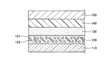
図1は、本発明の有機LED素子の一例を示す断面図である。 FIG. 1 is a cross-sectional view showing an example of the organic LED element of the present invention.
図1に示す例では、有機LED素子は、ボトムエミッションタイプの有機LED素子であって、基板110と、散乱層120と、第1の電極130と、有機層140と、第2の電極150とを順次有する。第1の電極130は、透明電極(陽極)であり、有機層140から発光された光を散乱層120へ伝えるための透明性を有する。一方、第2の電極150は、反射電極(陰極)であり、有機層140から発光された光を反射して有機層140へ戻すための反射性を有する。
In the example illustrated in FIG. 1, the organic LED element is a bottom emission type organic LED element, and includes a
尚、図1に示す例では、第1の電極130を陽極とし、第2の電極150を陰極としたが、第1の電極130を陰極とし、第2の電極150を陽極としても良い。
In the example shown in FIG. 1, the
(基板)
基板110は、透光性を有する。基板110(以下、「透光性基板110」という)は、可視光に対する透過率が高い材料で構成され、例えばガラスやプラスチックで構成される。(substrate)
The
透光性基板110を構成するガラスとしては、アルカリガラス、無アルカリガラス及び石英ガラスなどがある。一般的には、ソーダライムガラスが用いられる。一般的なソーダライムガラスは、50〜300℃における平均線膨張係数(以下、単に「平均線膨張係数」ともいう)が87×10−7/℃程度であり、徐冷点が550℃程度である。このようなソーダライムガラスで構成された透光性基板110は、550℃以上の温度で熱処理すると変形するおそれがあるので、散乱層120等を550℃よりも低い温度で形成することが好ましい。Examples of the glass constituting the light-transmitting
透光性基板110をプラスチック基板で構成した場合、プラスチック基板は、ガラス基板に比較して耐湿性が低いので、バリア性をもたせた構成としてもよい。例えば、透光性基板110は、プラスチック基板上の散乱層120側と反対側に別のガラス層を更に形成した構成としてもよい。
In the case where the light-transmitting
透光性基板110の厚さは、通常0.1mm〜2.0mmである。透光性基板110であるガラス基板が薄い場合には強度が不足するおそれがある。透光性基板110であるガラス基板の厚さは、0.5mm〜1.0mmであることが特に好ましい。
The thickness of the
透光性基板110上には、散乱層120が形成されている。透光性基板110であるガラス基板上の散乱層形成面は、シリカコーティング等の表面処理が施されたものであってもよい。即ち、透光性基板110であるガラス基板と散乱層120との間には、シリカ膜等の保護層が形成されていてもよい。
A
(第1の電極)
第1の電極(陽極)130は、有機層140で発生した光を外部に取り出すために、80%以上の透光性が要求される。また、多くの正孔を注入するため、仕事関数が高いものが要求される。具体的には、ITO(Indium Tin Oxide)、SnO2、ZnO、IZO(Indium Zinc Oxide)、AZO(ZnO−Al2O3:アルミニウムがドーピングされた亜鉛酸化物)、GZO(ZnO−Ga2O3:ガリウムがドーピングされた亜鉛酸化物)、NbドープTiO2、TaドープTiO2などの材料が用いられる。(First electrode)
The first electrode (anode) 130 is required to have a translucency of 80% or more in order to extract light generated in the
第1の電極130の厚さは、100nm以上であることが好ましい。100nm未満では、電気抵抗が高くなる。
The thickness of the
第1の電極130の屈折率は、通常、1.9〜2.2である。第1の電極130であるITOの屈折率を低下させるため、ITOのキャリア濃度を増加させてもよい。具体的には、ITOのSn濃度を増やすことで、ITOの屈折率を下げることができる。但し、Sn濃度を増やすと、移動度及び透過率が低下するので、これらのバランスをとって、Sn濃度を決める必要がある。
The refractive index of the
なお、第1の電極130は、単層であっても複数層であっても良いことは言うまでもない。
Needless to say, the
第1の電極130上には、有機層140が形成されている。
An
(有機層)
有機層140は、発光機能を有する層であり、正孔注入層と、正孔輸送層と、発光層と、電子輸送層と、電子注入層とにより構成される。(Organic layer)
The
正孔注入層は、陽極からの正孔注入障壁を低くするために、イオン化ポテンシャルの差が小さいものが要求される。正孔注入層における電極界面からの電荷の注入効率の向上は、素子の駆動電圧を下げるとともに、電荷の注入効率を高める。高分子では、ポリスチレンスルフォン酸(PSS)がドープされたポリエチレンジオキシチオフェン(PEDOT:PSS)、低分子ではフタロシアニン系の銅フタロシアニン(CuPc)が広く用いられる。 The hole injection layer is required to have a small difference in ionization potential in order to lower the hole injection barrier from the anode. Improvement of the charge injection efficiency from the electrode interface in the hole injection layer lowers the drive voltage of the device and increases the charge injection efficiency. Polyethylene dioxythiophene (PEDOT: PSS) doped with polystyrene sulfonic acid (PSS) is widely used for polymers, and phthalocyanine-based copper phthalocyanine (CuPc) is widely used for low molecules.
正孔輸送層は、正孔注入層から注入された正孔を発光層に輸送する役割をする。適切なイオン化ポテンシャルと正孔移動度を有することが必要である。正孔輸送層は、具体的には、トリフェニルアミン誘導体、N,N'−ビス(1−ナフチル)−N,N'−ジフェニル−1,1'−ビフェニル−4,4'−ジアミン(NPD)、N,N'−ジフェニル−N,N'−ビス[N−フェニル−N−(2−ナフチル)−4'−アミノビフェニル−4−イル]−1,1'−ビフェニル−4,4'−ジアミン(NPTE)、1,1−ビス[(ジ−4−トリルアミノ)フェニル]シクロヘキサン(HTM2)およびN,N'−ジフェニル−N,N'−ビス(3−メチルフェニル)−1,1'−ジフェニル−4,4'−ジアミン(TPD)などが用いられる。正孔輸送層の厚さは、10nm〜150nmが好ましい。厚さは薄ければ薄いほど低電圧化できるが、電極間短絡の問題から10nm〜150nmであることが特に好ましい。 The hole transport layer serves to transport holes injected from the hole injection layer to the light emitting layer. It is necessary to have an appropriate ionization potential and hole mobility. Specifically, the hole transport layer may be a triphenylamine derivative, N, N′-bis (1-naphthyl) -N, N′-diphenyl-1,1′-biphenyl-4,4′-diamine (NPD ), N, N′-diphenyl-N, N′-bis [N-phenyl-N- (2-naphthyl) -4′-aminobiphenyl-4-yl] -1,1′-biphenyl-4,4 ′ -Diamine (NPTE), 1,1-bis [(di-4-tolylamino) phenyl] cyclohexane (HTM2) and N, N'-diphenyl-N, N'-bis (3-methylphenyl) -1,1 ' -Diphenyl-4,4'-diamine (TPD) or the like is used. The thickness of the hole transport layer is preferably 10 nm to 150 nm. The thinner the thickness is, the lower the voltage can be. However, the thickness is particularly preferably 10 nm to 150 nm from the problem of short circuit between electrodes.
発光層は、注入された電子と正孔が再結合する場を提供し、かつ、発光効率の高い材料を用いる。詳細に説明すると、発光層に用いられる発光ホスト材料および発光色素のドーピング材料は、陽極及び陰極から注入された正孔及び電子の再結合中心として機能する、また、発光層におけるホスト材料への発光色素のドーピングは、高い発光効率を得ると共に、発光波長を変換させる。これらは電荷注入のための適切なエネルギーレベルを有すること、化学的安定性や耐熱性に優れ、均質なアモルファス薄膜を形成することなどが求められる。また、発光色の種類や色純度が優れていることや発光効率の高いことが求められる。有機材料である発光材料には、低分子系と高分子系の材料がある。さらに、発光機構によって、蛍光材料、りん光材料に分類される。発光層は、具体的には、トリス(8−キノリノラート)アルミニウム錯体(Alq3)、ビス(8−ヒドロキシ)キナルジンアルミニウムフェノキサイド(Alq′2OPh)、ビス(8−ヒドロキシ)キナルジンアルミニウム−2,5−ジメチルフェノキサイド(BAlq)、モノ(2,2,6,6−テトラメチル−3,5−ヘプタンジオナート)リチウム錯体(Liq)、モノ(8−キノリノラート)ナトリウム錯体(Naq)、モノ(2,2,6,6−テトラメチル−3,5−ヘプタンジオナート)リチウム錯体、モノ(2,2,6,6−テトラメチル−3,5−ヘプタンジオナート)ナトリウム錯体およびビス(8−キノリノラート)カルシウム錯体(Caq2)などのキノリン誘導体の金属錯体、テトラフェニルブタジエン、フェニルキナクドリン(QD)、アントラセン、ペリレン並びにコロネンなどの蛍光性物質が挙げられる。ホスト材料としては、キノリノラート錯体が好ましく、特に、8−キノリノールおよびその誘導体を配位子としたアルミニウム錯体が好ましい。 The light-emitting layer uses a material that provides a field where injected electrons and holes are recombined and has high emission efficiency. More specifically, the light-emitting host material and the light-emitting dye doping material used in the light-emitting layer function as recombination centers of holes and electrons injected from the anode and the cathode, and light emission to the host material in the light-emitting layer The doping of the dye obtains high luminous efficiency and converts the emission wavelength. These are required to have an appropriate energy level for charge injection, to form a uniform amorphous thin film having excellent chemical stability and heat resistance. In addition, it is required that the type and color purity of the luminescent color are excellent and the luminous efficiency is high. Light emitting materials that are organic materials include low-molecular materials and high-molecular materials. Further, it is classified into a fluorescent material and a phosphorescent material according to the light emission mechanism. Specifically, the light-emitting layer includes tris (8-quinolinolato) aluminum complex (Alq3), bis (8-hydroxy) quinaldine aluminum phenoxide (Alq′2OPh), bis (8-hydroxy) quinaldine aluminum-2, 5-dimethylphenoxide (BAlq), mono (2,2,6,6-tetramethyl-3,5-heptanedionate) lithium complex (Liq), mono (8-quinolinolato) sodium complex (Naq), mono ( 2,2,6,6-tetramethyl-3,5-heptanedionate) lithium complex, mono (2,2,6,6-tetramethyl-3,5-heptanedionate) sodium complex and bis (8- Quinolinolates) metal complexes of quinoline derivatives such as calcium complexes (Caq2), tetraphenylbutadiene, Rukinakudorin (QD), anthracene, and a fluorescent substance such as perylene and coronene. As the host material, a quinolinolate complex is preferable, and an aluminum complex having 8-quinolinol and a derivative thereof as a ligand is particularly preferable.
電子輸送層は、電極から注入された電子を輸送するという役割をする。電子輸送層は、具体的には、キノリノールアルミニウム錯体(Alq3)、オキサジアゾール誘導体(例えば、2,5−ビス(1−ナフチル)−1,3,4−オキサジアゾール(BND)および2−(4−t−ブチルフェニル)−5−(4−ビフェニル)−1,3,4−オキサジアゾール(PBD)など)、トリアゾール誘導体、バソフェナントロリン誘導体、シロール誘導体などが用いられる。 The electron transport layer serves to transport electrons injected from the electrode. Specifically, the electron transport layer includes a quinolinol aluminum complex (Alq3), an oxadiazole derivative (for example, 2,5-bis (1-naphthyl) -1,3,4-oxadiazole (BND) and 2- (4-t-butylphenyl) -5- (4-biphenyl) -1,3,4-oxadiazole (PBD) and the like), triazole derivatives, bathophenanthroline derivatives, silole derivatives, and the like are used.
電子注入層は、電子の注入効率を高めるものが要求される。電子注入層は、具体的には、陰極界面にリチウム(Li)、セシウム(Cs)等のアルカリ金属をドープした層を設ける。 The electron injection layer is required to increase the electron injection efficiency. Specifically, the electron injection layer is provided with a layer doped with an alkali metal such as lithium (Li) or cesium (Cs) at the cathode interface.
有機層140の屈折率は、通常、1.7〜1.8である。
The refractive index of the
有機層140上には、第2の電極150が形成されている。
A
(第2の電極)
第2の電極(陰極)150は、反射性が要求されるので、仕事関数の小さな金属またはその合金が用いられる。第2の電極150は、具体的には、アルカリ金属、アルカリ土類金属及び周期表第3族の金属などが挙げられる。このうち、安価で化学的安定性の良い材料であることから、アルミニウム(Al)、マグネシウム(Mg)、銀(Ag)またはこれらの合金などが好ましく用いられる。また、Al、MgAgの共蒸着膜、LiFまたはLi2Oの薄膜蒸着膜の上にAlを蒸着した積層電極等が用いられる。また、高分子系では、カルシウム(Ca)またはバリウム(Ba)とアルミニウム(Al)の積層等が用いられる。(Second electrode)
Since the second electrode (cathode) 150 is required to have reflectivity, a metal having a small work function or an alloy thereof is used. Specific examples of the
(散乱層)
散乱層120は、透光性基板110と第1の電極130との間に設けられる。(Scattering layer)
The
散乱層120を介さずに、透光性基板110上に第1の電極130を形成した場合、一般に、透光性基板110は第1の電極130よりも屈折率が低いので、透光性基板110に浅い角度で進入しようとした光は、スネルの法則により有機層140側に全反射される。全反射された光は、第2の電極150である反射電極で再び反射され、透光性基板110に再び到達する。このとき、透光性基板110への再入射角度は変わらないので、有機LED素子の外部に光を取り出せなくなる。
When the
これに対し、本実施形態では、散乱層120が透光性基板110と第1の電極130との間に設けられているので、透光性基板110への再入射角度を変えることができ、有機LED素子の光取り出し効率を高めることができる。
On the other hand, in this embodiment, since the
散乱層120は、図1に示すように、ベース材121中に、ベース材121と異なる屈折率を有する1種以上の散乱材122が分散されたものである。
As shown in FIG. 1, the
ベース材121の屈折率は、第1の電極130の屈折率と同等若しくは高いことが好ましい。ベース材121の屈折率が低い場合、散乱層120と第1の電極130との界面において、全反射による損失が生じてしまうために光取り出し効率が低下するからである。ベース材121の屈折率は、少なくとも有機層140の発光スペクトル範囲における一部分(例えば、赤、青、緑など)において上回っていれば良いが、発光スペクトル範囲全域(430nm〜650nm)に亘って上回っていることが好ましく、可視光の波長範囲全域(360nm〜830nm)に亘って上回っていることがより好ましい。なお、以下では特に断らない限り、「屈折率」とは、Heランプd線(波長:587.6nm)で25℃で測定した屈折率を意味する。
The refractive index of the
ベース材121と散乱材122の屈折率の差は、少なくとも発光層の発光スペクトル範囲における一部分において0.05以上であることが好ましい。十分な散乱特性を得るために、屈折率の差は、発光スペクトル範囲全域(430nm〜650nm)若しくは可視光の波長範囲全域(360nm〜830nm)に亘って0.05以上であることがより好ましい。
The difference in refractive index between the
散乱材122は、散乱層120に占める割合が1〜85体積%であることが好ましい。1体積%未満であると、十分な散乱効果が得られず、光取り出し効率の向上効果も少ないからである。より好ましくは、20体積%以上である。一方、85体積%より多過ぎると、光取り出し効率が低下するおそれがある。より好ましくは、80体積%以下である。さらに好ましくは30体積%以下である。
The ratio of the
ここで、散乱層120に占める散乱材122の割合とは、散乱層120中に複数種の散乱材が分散されている場合、全ての散乱材の割合の合計をいう。
Here, the ratio of the
散乱材122の形状は、特に制限されないが、散乱材122が球形である場合、その直径の平均値は0.1〜10μmであることが好ましい。0.1μmより小さいと、光散乱材として十分に機能しない。一方、10μmより大きいと、散乱層120全体に均質に存在させることが困難になり、光取り出し効率のムラが発生する。また、相対的に散乱材122の数が少なくなる部分において、散乱性が低下する。また、塗布焼成膜の表面平滑性が得られなくなる。散乱材122は、最大長さが10μm以上のものの割合が15体積%以下であることがより望ましい。さらに望ましくは10体積%以下である。
The shape of the
散乱層120上には、第1の電極130が形成されている。散乱層120上の第1の電極形成面の表面粗さRaは、30nm以下であるのが好ましく、10nm以下であるのがより好ましく、1nm以下であるのが特に好ましい。30nmを超えると、第1の電極130や有機層140の平滑性が損なわれ、第1の電極130と第2の電極150との間で短絡が発生するおそれがある。ここで、表面粗さRaとは、微視的にみた表面粗さであり、JIS B 0601−2001に規定されている輪郭曲線フィルタの長波長カットオフ値λcを10μmとした値であって、例えば原子間力顕微鏡(AFM)などで測定されるものである。
A
散乱層120上の第1の電極形成面は、平坦性を向上するため、コーティングが施されたものであっても良い。
The first electrode formation surface on the
(散乱層の散乱材)
散乱材122としては、気泡、ベース材121と異なる屈折率を有する材料の粒子が用いられる。ここで、粒子とは固体の小さな物質をいい、例えば、ガラスやその他のセラミックがある。また、気泡とは、空気若しくはガスの物体をいう。なお、散乱材122が気泡の場合、散乱材122の径とは空隙の長さをいう。(Scattering material for scattering layer)
As the
(散乱層のベース材)
ベース材121としては、ガラスが用いられる。ベース材121がガラスで構成されているので、散乱層120の散乱特性を高めつつ、散乱層120の表面の平滑性と透明性を維持することができる。(Base material for scattering layer)
As the
ベース材121に用いられるガラス(以下、「ベース材ガラス」という)は、酸化物基準のモル%表示で、P2O5を0〜20%、B2O3を15〜60%、Bi2O3を10〜37%、ZnOを5〜50%、SiO2を0〜20%、Al2O3を0〜10%、ZrO2を0〜5%、Gd2O3を0〜10%、TiO2を0〜15%、MgOとCaOとSrOとBaOを合計で0〜10%含有し、P2O5の含有量をZnOの含有量で割った値が0.48未満であり、P2O5とB2O3の含有量の合量が30〜60%であり、P2O5とB2O3の含有量の合量が50%を超えるときはP2O5の含有量は10%以下であり、不純物として含有されることを除き、鉛(PbOまたはPb3O4)とLi2OとNa2OとK2Oを実質的に含有しない。The glass used for the base material 121 (hereinafter referred to as “base material glass”) is expressed in terms of mol% based on oxides, P 2 O 5 is 0 to 20%, B 2 O 3 is 15 to 60%, Bi 2. 10 to 37% O 3 , 5 to 50% ZnO, 0 to 20% SiO 2 , 0 to 10% Al 2 O 3 , 0 to 5% ZrO 2 , 0 to 10% Gd 2 O 3 In addition, 0 to 15% of TiO 2 , 0 to 10% of MgO, CaO, SrO and BaO in total, and a value obtained by dividing the content of P 2 O 5 by the content of ZnO is less than 0.48, a P 2 O 5 and B total content of 2 O 3 is 30% to 60%, when the total content of P 2 O 5 and B 2 O 3 exceeds 50% of the P 2 O 5 content is more than 10%, except that it is contained as an impurity, lead (PbO or Pb 3 O 4) and the Li 2 O It does not substantially contain a 2 O and K 2 O.
次に、このベース材ガラスのガラス組成について説明する。なお、単位%は、モル%を意味する。 Next, the glass composition of this base material glass will be described. The unit% means mol%.
Bi2O3は、屈折率を上げ、粘性を下げる成分であり、含有量が10%未満では、散乱層120の屈折率が低くなり過ぎる。一方、Bi2O3含有量が37%超では、平均線膨張係数が大きくなり過ぎるとともに、焼成工程で結晶化しやすい。Bi2O3含有量は、15〜28%が好ましい。Bi 2 O 3 is a component that increases the refractive index and decreases the viscosity. If the content is less than 10%, the refractive index of the
B2O3はガラスの骨格となる成分であり、含有量が15%未満では、ガラス成形時に失透しやすく、フリット化した後の焼成時に結晶化しやすくなる。B2O3含有量が60%超では、耐水性が低下する。B 2 O 3 is a component that becomes a skeleton of the glass. If the content is less than 15%, it tends to be devitrified at the time of glass forming and easily crystallized at the time of baking after frit formation. When the B 2 O 3 content exceeds 60%, the water resistance decreases.
ZnOは、ガラスを安定化させる成分であり、含有量が5%未満では、ガラス成形時に失透しやすくなるとともに、ガラス転移点が高くなり、フリット焼成膜の平滑性が得られなくなる。また、屈折率が低下し好ましくない。ZnO含有量が50%超では、平均線膨張係数が大きくなるとともに、ガラス成形時に失透しやすくなる。耐候性が低下するおそれがある。ZnO含有量は、20〜50%が好ましい。 ZnO is a component that stabilizes glass. When the content is less than 5%, devitrification easily occurs during glass molding, and the glass transition point becomes high, and the smoothness of the frit-fired film cannot be obtained. In addition, the refractive index decreases, which is not preferable. If the ZnO content is more than 50%, the average linear expansion coefficient increases, and devitrification easily occurs during glass forming. Weather resistance may be reduced. The ZnO content is preferably 20 to 50%.
SiO2は、ガラスの安定性を高めるとともに、平均線膨張係数を小さくする任意成分である。SiO2含有量は、0〜20%が好ましい。20%超であると、屈折率が低下し過ぎるおそれがある。SiO 2 is an optional component that increases the stability of the glass and decreases the average linear expansion coefficient. The SiO 2 content is preferably 0 to 20%. If it exceeds 20%, the refractive index may be too low.
Al2O3は、ガラスの安定性を高める任意成分である。Al2O3の含有量は、0〜10%が好ましい。10%超であると、液相温度が上がり、失透するおそれがある。Al 2 O 3 is an optional component that increases the stability of the glass. The content of Al 2 O 3 is preferably 0 to 10%. If it exceeds 10%, the liquidus temperature increases and devitrification may occur.
P2O5はガラスの骨格となる成分であり、耐酸性を向上させる任意成分である。P2O5含有量は、0〜20%が好ましい。20%超では、ガラス成形時に失透しやすく、フリット化した後の焼成時に結晶化しやすくなる。また、屈折率が低下する。P2O5の含有量が0%であると、結晶化を特に抑制でき、より広い温度範囲で結晶化を伴わずにフリットの焼成を行なうことができるため好ましい。なお、耐酸性向上の効果を期待する場合は、2%以上含有することがより望ましく、5%以上含有することがさらに望ましい。P 2 O 5 is a component that becomes a glass skeleton, and is an optional component that improves acid resistance. The P 2 O 5 content is preferably 0 to 20%. If it exceeds 20%, it tends to be devitrified at the time of glass molding, and it is easy to crystallize at the time of baking after frit formation. In addition, the refractive index decreases. When the content of P 2 O 5 is 0%, crystallization can be particularly suppressed, and the frit can be fired without crystallization in a wider temperature range, which is preferable. In addition, when the effect of improving acid resistance is expected, the content is more preferably 2% or more, and further preferably 5% or more.
ZrO2はガラスの耐候性を高める任意成分であり、ZrO2の含有量は0〜5%が好ましい。5%超であると、結晶化しやすくなるとともに、ガラス転移点が高くなり過ぎるおそれがある。ZrO 2 is an optional component that enhances the weather resistance of the glass, and the content of ZrO 2 is preferably 0 to 5%. If it exceeds 5%, crystallization is likely to occur and the glass transition point may be too high.
Gd2O3は、平均線膨張係数を低く抑えながら屈折率を上げるとともに軟化点付近での結晶化を抑制する任意成分である。Gd2O3の含有量は、0〜10%が好ましい。10%超であると、結晶化し易く、ガラス転移点と軟化点が上がるおそれがある。特に、低膨張と高屈折率を両立したい場合、2%以上含有することがより望ましい。Gd 2 O 3 is an optional component that increases the refractive index while suppressing the average linear expansion coefficient low and suppresses crystallization near the softening point. The content of Gd 2 O 3 is preferably 0 to 10%. If it exceeds 10%, crystallization tends to occur, and the glass transition point and the softening point may be increased. In particular, when it is desired to achieve both low expansion and high refractive index, it is more desirable to contain 2% or more.
TiO2は、必須ではないが、屈折率を上げる成分であり、15%まで含有しても良い。ただし、過剰に含有すると、結晶化し易く、ガラス転移点と軟化点が上がるおそれがある。なお、TiO2の代わりに(または加えて)WO3を使用することも可能である。TiO2とWO3の含有量の合量は、0〜12%がより望ましい。TiO 2 is not essential, but is a component that increases the refractive index, and may be contained up to 15%. However, when it contains excessively, it will crystallize easily and there exists a possibility that a glass transition point and a softening point may rise. It is also possible to use WO 3 instead of (or in addition to) TiO 2 . The total content of TiO 2 and WO 3 is more preferably 0 to 12%.
アルカリ土類金属酸化物(MgO、CaO、SrO及びBaO)は、ガラスの粘性を下げる任意成分である。アルカリ土類金属酸化物の含有量は、0〜10%が好ましい。10%超であると、平均線膨張係数が大きくなり、屈折率が下がるおそれがある。7%以下であることがより好ましい。 Alkaline earth metal oxides (MgO, CaO, SrO and BaO) are optional components that lower the viscosity of the glass. The content of the alkaline earth metal oxide is preferably 0 to 10%. If it exceeds 10%, the average linear expansion coefficient tends to increase, and the refractive index may decrease. More preferably, it is 7% or less.
Li2O、Na2O及びK2Oは、実質的に含まれない。これらのアルカリ金属酸化物が含まれると、熱処理工程において、そのアルカリ成分が拡散するおそれがある。そして、そのアルカリ成分は、素子へ電気的な悪影響を与える場合がある。Li 2 O, Na 2 O and K 2 O are not substantially contained. When these alkali metal oxides are contained, the alkali component may be diffused in the heat treatment step. The alkali component may have an electrical adverse effect on the device.
ここで、実質的に含まないとは、不純物として含まれるのを除き、積極的に含有しないことをいう。 Here, “substantially not containing” means not actively containing, except for being contained as an impurity.
PbOとPb3O4は、実質的に含まれない。PbO and Pb 3 O 4 are not substantially contained.
P2O5の含有量をZnOの含有量で割った値は、0.48未満である。0.48以上では失透し易くなり、結晶化し易くなるおそれがある。また、0.48以上では屈折率が下がり、ガラス転移点と軟化点が上がるおそれがある。The value obtained by dividing the content of P 2 O 5 by the content of ZnO is less than 0.48. If it is 0.48 or more, devitrification tends to occur and crystallization tends to occur. On the other hand, if it is 0.48 or more, the refractive index decreases, and the glass transition point and softening point may increase.
P2O5とB2O3の含有量の合量は30〜60%である。30%未満では失透し易くなり、結晶化し易くなり、安定性を損なうおそれがある。一方、60%超では失透し易くなり、結晶化し易くなり、屈折率が下がるおそれがある。ここで、P2O5とB2O3の含有量の合量が50%を超える場合、P2O5の含有量は10%以下である。10%超では失透し易くなり、結晶化し易くなる。The total content of P 2 O 5 and B 2 O 3 is 30 to 60%. If it is less than 30%, devitrification tends to occur, crystallization tends to occur, and stability may be impaired. On the other hand, if it exceeds 60%, devitrification tends to occur, crystallization is likely to occur, and the refractive index may decrease. Here, when the total content of P 2 O 5 and B 2 O 3 exceeds 50%, the content of P 2 O 5 is 10% or less. If it exceeds 10%, devitrification tends to occur and crystallization tends to occur.
ベース材ガラスは、発明の効果を失わない範囲で、上記成分の他、例えば、GeO2、Nb2O5、Y2O3、Ce2O3、CeO2、La2O3、TeO2、SnO、SnO2、Sb2O3、Ta2O5等を含んでいてもよい。ただし、それらは合計で5%までにとどめることが好ましい。また、色味を調整するために、微量の着色剤を含有していてもよい。着色剤としては、遷移金属酸化物、希土類金属酸化物、金属コロイドなどの公知のものが用いられる。これらの着色剤は、単独であるいは組み合わせて用いられる。As long as the base material glass does not lose the effect of the invention, in addition to the above components, for example, GeO 2 , Nb 2 O 5 , Y 2 O 3 , Ce 2 O 3 , CeO 2 , La 2 O 3 , TeO 2 , SnO, may contain SnO 2, Sb 2 O 3, Ta 2 O 5 or the like. However, it is preferable to limit them to 5% in total. Moreover, in order to adjust a color, you may contain a trace amount coloring agent. As the colorant, known ones such as transition metal oxides, rare earth metal oxides, and metal colloids are used. These colorants are used alone or in combination.
次に、このベース材ガラスの特性について説明する。 Next, the characteristic of this base material glass is demonstrated.
ベース材ガラスの屈折率ndは、1.75以上が好ましく、1.80以上がより好ましく、1.85以上が特に好ましい。1.75未満であると、散乱層120と第1の電極130との界面において、全反射による損失が大きく、光取り出し効率が低下しやすい。Refractive index n d of the base material glass is preferably 1.75 or more, more preferably 1.80 or more, particularly preferably 1.85 or more. If it is less than 1.75, the loss due to total reflection is large at the interface between the
ベース材ガラスのガラス軟化点Tsは、600℃以下が好ましく、595℃以下がより好ましく、590℃以下が特に好ましい。 The glass softening point Ts of the base material glass is preferably 600 ° C. or less, more preferably 595 ° C. or less, and particularly preferably 590 ° C. or less.
ベース材ガラスのガラス転移点Tgは、透光性基板110がソーダライムガラスで構成される場合、透光性基板110の熱変形を抑制するため、500℃以下が好ましく、495℃以下がより好ましく、485℃以下が特に好ましい。
When the
ベース材ガラスの結晶化ピーク温度Tcは、結晶化を抑制する観点から、600℃以上が好ましく、650℃以上がより好ましく、700℃以上が特に好ましい。 From the viewpoint of suppressing crystallization, the crystallization peak temperature Tc of the base material glass is preferably 600 ° C. or higher, more preferably 650 ° C. or higher, and particularly preferably 700 ° C. or higher.
ベース材ガラスの結晶化ピーク温度Tcとガラス軟化温度Tsとの差(Tc−Ts)は、結晶化を抑制する観点から、55℃以上が好ましく、70℃以上がより好ましく、90℃以上が特に好ましい。 The difference between the crystallization peak temperature Tc of the base material glass and the glass softening temperature Ts (Tc−Ts) is preferably 55 ° C. or higher, more preferably 70 ° C. or higher, particularly 90 ° C. or higher, from the viewpoint of suppressing crystallization. preferable.
ベース材ガラスの50〜300℃における平均線膨張係数αは、透光性基板110がソーダライムガラスで構成される場合、ソーダライムガラスの破損や反りを防止するため、60×10−7/℃以上が好ましく、65×10−7/℃以上がより好ましい。また、ベース材ガラスの50〜300℃における平均線膨張係数αは、100×10−7/℃以下が好ましく、90×10−7/℃以下がより好ましい。The average linear expansion coefficient α of the base material glass at 50 to 300 ° C. is 60 × 10 −7 / ° C. in order to prevent the soda lime glass from being damaged or warped when the
このベース材ガラスは、酸化物、リン酸塩、メタリン酸塩、炭酸塩、硝酸塩、水酸化物等の原料を秤取し、混合した後、白金等の坩堝を用いて900〜1400℃の温度で溶解し、冷却することによって得ることができる。その後、必要に応じて徐冷して歪みを取り除く場合がある。得られたベース材ガラスを乳鉢、ボールミル、ジェットミル等により粉砕し、必要に応じて分級することによってベース材ガラスの粉末が得られる。ベース材ガラスの粉末の表面を、界面活性剤やシランカップリング剤によって改質して用いても良い。 This base material glass is prepared by weighing and mixing raw materials such as oxides, phosphates, metaphosphates, carbonates, nitrates and hydroxides, and then using a crucible such as platinum at a temperature of 900 to 1400 ° C. It can be obtained by dissolving in and cooling. Thereafter, it may be gradually cooled as necessary to remove distortion. The obtained base material glass is pulverized with a mortar, ball mill, jet mill or the like, and classified as necessary to obtain a base material glass powder. The surface of the base material glass powder may be modified with a surfactant or a silane coupling agent.
(散乱層の製造方法)
散乱層120は、ガラスフリットを透光性基板110上に塗布し、焼成することによって、製造することができる。(Manufacturing method of scattering layer)
The
(1)ガラスフリット
ガラスフリットは、上記ベース材ガラスの粉末を含むものである。ベース材ガラスの粉末の粒径は、塗工性の観点から、1〜10μmであることが好ましい。ベース材ガラスの粉末の表面は、界面活性剤やシランカップリング剤によって改質されたものであってもよい。(1) Glass frit Glass frit contains the powder of the said base material glass. The particle size of the base material glass powder is preferably 1 to 10 μm from the viewpoint of coatability. The surface of the base material glass powder may be modified with a surfactant or a silane coupling agent.
ガラスフリットは、ベース材ガラスの粉末の他に、散乱材122として、ベース材ガラスよりも低い屈折率を有するガラスの粉末を含むものであってもよい。
The glass frit may include glass powder having a lower refractive index than the base material glass as the
ガラスフリットは、塗工性の観点から、樹脂や溶剤などと混練されたフリットペーストとして、透光性基板110上に塗布されることが好ましい。
The glass frit is preferably applied on the light-transmitting
(2)フリットペースト
フリットペーストは、ガラスフリットとビヒクルとを、プラネタリーミキサー等で混合し、3本ロール等で均一に分散させて得られる。粘度調整のため、混練機で更に混練してもよい。通常、ガラスフリットを70〜80質量%、ビヒクルを20〜30質量%の割合で混合する。(2) Frit paste A frit paste is obtained by mixing glass frit and a vehicle with a planetary mixer or the like and uniformly dispersing them with a three roll or the like. You may further knead | mix with a kneading machine for viscosity adjustment. Usually, the glass frit is mixed at a ratio of 70 to 80% by mass and the vehicle at a ratio of 20 to 30% by mass.
ここで、ビヒクルとは、樹脂、溶剤を混合したものをいい、界面活性剤を更に混合したものを含む。具体的には、50〜80℃に加熱した溶剤中に樹脂、界面活性剤などを投入し、その後4時間から12時間程度静置したのち、ろ過し、得られる。 Here, the vehicle means a mixture of a resin and a solvent, and includes a mixture of a surfactant. Specifically, a resin, a surfactant, or the like is put into a solvent heated to 50 to 80 ° C., and then allowed to stand for about 4 to 12 hours, followed by filtration.
樹脂は、塗布後のフリットペースト膜を保形するためのものである。具体例としては、エチルセルロース、ニトロセルロース、アクリル樹脂、酢酸ビニル、ブチラール樹脂、メラミン樹脂、アルキッド樹脂、ロジン樹脂などが用いられる。主剤として用いられるのは、エチルセルロースとニトロセルロースがある。なお、ブチラール樹脂、メラミン樹脂、アルキッド樹脂、ロジン樹脂は塗膜強度向上の為の添加として用いられる。焼成時の脱バインダ温度は、エチルセルロースで350〜400℃、ニトロセルロースで200〜300℃である。 The resin is for retaining the frit paste film after application. Specific examples include ethyl cellulose, nitrocellulose, acrylic resin, vinyl acetate, butyral resin, melamine resin, alkyd resin, and rosin resin. There are ethyl cellulose and nitrocellulose as main agents. Butyral resin, melamine resin, alkyd resin, and rosin resin are used as additives for improving the strength of the coating film. The binder removal temperature during firing is 350 to 400 ° C. for ethyl cellulose and 200 to 300 ° C. for nitrocellulose.
溶剤は、樹脂を溶解すると共にフリットペーストの粘度を調整するためのものである。溶剤は、塗工中には乾燥せず、乾燥中にはすばやく乾燥するものが好ましく、沸点が200〜230℃のものが好ましい。具体例としては、エーテル系溶剤(ブチルカルビトール(BC)、ブチルカルビトールアセテート(BCA)、ジエチレングリコールジ−n−ブチルエーテル、ジプロピレングリコールブチルエーテル、トリプロピレングリコールブチルエーテル、酢酸ブチルセロソルブ)、アルコール系溶剤(α−テルピネオール、パインオイル、ダワノール)、エステル系溶剤(2,2,4−トリメチル−1,3−ペンタンジオールモノイソブチレート)、フタル酸エステル系溶剤(DBP(ジブチルフタレート)、DMP(ジメチルフタレート)、DOP(ジオクチルフタレート))がある。これらの溶剤は、単独で用いられてもよいし、粘度、固形分比、乾燥速度調整のため、組み合わせて用いられてもよい。主に用いられているのは、α−テルピネオールや2,2,4−トリメチル−1,3−ペンタンジオールモノイソブチレート)である。なお、DBP(ジブチルフタレート)、DMP(ジメチルフタレート)、DOP(ジオクチルフタレート)は、可塑剤としても機能する。 The solvent is for dissolving the resin and adjusting the viscosity of the frit paste. The solvent is preferably not dried during coating, but quickly dried during drying, and preferably has a boiling point of 200 to 230 ° C. Specific examples include ether solvents (butyl carbitol (BC), butyl carbitol acetate (BCA), diethylene glycol di-n-butyl ether, dipropylene glycol butyl ether, tripropylene glycol butyl ether, butyl cellosolve acetate), alcohol solvents (α -Terpineol, pine oil, Dawanol), ester solvent (2,2,4-trimethyl-1,3-pentanediol monoisobutyrate), phthalate ester solvent (DBP (dibutyl phthalate), DMP (dimethyl phthalate) , DOP (dioctyl phthalate)). These solvents may be used alone or in combination for adjusting the viscosity, the solid content ratio, and the drying speed. Mainly used are α-terpineol and 2,2,4-trimethyl-1,3-pentanediol monoisobutyrate). DBP (dibutyl phthalate), DMP (dimethyl phthalate), and DOP (dioctyl phthalate) also function as a plasticizer.
(3)塗布
フリットペーストを透光性基板110上に塗布する方法としては、スクリーン印刷、ドクターブレード印刷、ダイコート印刷等が用いられる。また、フリットペーストをPETフィルム等に塗布して乾燥してグリーンシートとし、グリーンシートを透光性基板110上に熱圧着してもよい。(3) Application As a method for applying the frit paste onto the
スクリーン印刷を用いる場合、スクリーン版のメッシュ粗さ、乳剤の厚み、印刷時の押し圧、スキージ押し込み量などを調節することにより、塗布後のフリットペースト膜の膜厚を制御できる。 When screen printing is used, the film thickness of the frit paste film after coating can be controlled by adjusting the mesh roughness of the screen plate, the thickness of the emulsion, the pressing pressure during printing, the amount of squeegee pressing.
ドクターブレード印刷、ダイコート印刷を用いる場合、スクリーン印刷を用いる場合と比較して、塗布後のフリットペースト膜の膜厚を厚くすることができる。 When doctor blade printing or die coat printing is used, the thickness of the frit paste film after application can be increased compared with the case where screen printing is used.
尚、塗布、乾燥を繰り返し行うことで、フリットペースト膜を厚くしてもよい。 The frit paste film may be thickened by repeatedly applying and drying.
(4)焼成
透光性基板110上に塗布されたフリットペーストを焼成する。焼成は、フリットペースト中の樹脂を分解・消失させる脱バインダ処理と、脱バインダ処理後のフリットペーストを焼結、軟化させる焼成処理とからなる。脱バインダ温度は、エチルセルロースで350〜400℃、ニトロセルロースで200〜300℃であり、30分から1時間大気雰囲気で加熱する。焼成温度(焼成処理温度)は、ベース材ガラスのガラス軟化点Tsを基準として−40℃〜+30℃の範囲内、あるいはベース材ガラスのガラス転移点Tgを基準として+50℃〜+120℃の範囲内に設定される。焼成後、室温まで冷却することによって透光性基板110上に散乱層120が形成される。(4) Firing The frit paste applied on the
焼成温度や焼成雰囲気、ガラスフリットの粒度分布などを調節することにより、散乱層120の内部に残存する気泡の形状、大きさを調節することができる。
By adjusting the firing temperature, the firing atmosphere, the particle size distribution of the glass frit, etc., the shape and size of the bubbles remaining in the
尚、散乱材122として、気泡の代わりに(又は気泡に加えて)、ベース材121と異なる屈折率を有する材料の粒子を用いる場合、該材料の粒子をガラスフリットに混ぜて透光性基板110上に塗布し焼成する。
In the case where particles of a material having a refractive index different from that of the
以下に、実施例により本発明を具体的に説明するが、本発明は以下の実施例によって限定されるものではない。 EXAMPLES The present invention will be specifically described below with reference to examples, but the present invention is not limited to the following examples.
(実験1)
例1〜例44については、表1〜表6中の組成のガラスが得られるように、H3BO3、ZnO、Bi2O3、TiO2、WO3、Zn(PO3)2、Li2CO3、Na2CO3、K2CO3、MgO、CaCO3、SrCO3、BaCO3、ZrO2、Gd2O3、SiO2、Al2O3の各粉末原料を合計で200gとなるよう秤取し、混合した後、白金坩堝を用いて、例1〜例25については1050℃で例26〜例44については1250℃で、1時間溶解し、続けて例1〜例25については950℃で例26〜例44については1100℃で、1時間溶解し、この融液の半量をカーボン鋳型に流しだしてバルク状のガラスを得、残りを双ロールの隙間に流しだして急冷しフレーク状のガラスを得た。また、バルク状ガラスは500℃の電気炉に入れ、1時間あたり100℃の速度で室温まで温度を下げることにより、歪みを取り除いた。(Experiment 1)
For Examples 1 to 44, H 3 BO 3 , ZnO, Bi 2 O 3 , TiO 2 , WO 3 , Zn (PO 3 ) 2 , Li so as to obtain glasses having the compositions in Tables 1 to 6 Each powder raw material of 2 CO 3 , Na 2 CO 3 , K 2 CO 3 , MgO, CaCO 3 , SrCO 3 , BaCO 3 , ZrO 2 , Gd 2 O 3 , SiO 2 , Al 2 O 3 will be 200 g in total. After being weighed and mixed, using a platinum crucible, melting was carried out for 1 hour at 1050 ° C. for Examples 1 to 25 and 1250 ° C. for Examples 26 to 44, and subsequently for Examples 1 to 25 For Example 26 to Example 44 at 950 ° C., melt at 1100 ° C. for 1 hour. Half of the melt is poured into a carbon mold to obtain a bulk glass, and the rest is poured into a gap between twin rolls to quench. Get flaky glass . The bulk glass was put in an electric furnace at 500 ° C., and the strain was removed by lowering the temperature to room temperature at a rate of 100 ° C. per hour.
ここで、例1〜例22及び例26〜例44は実施例であり、例23〜例25は比較例である。 Here, Examples 1 to 22 and Examples 26 to 44 are Examples, and Examples 23 to 25 are Comparative Examples.
得られたガラスについて、バルク作製時の失透の有無、フレーク作製時の失透の有無、フリット焼成時の結晶化の有無、屈折率nd、ガラス転移点Tg(単位:℃)、50〜300℃における平均線膨張係数α(単位:10−7/℃)、ガラス軟化点Ts(単位:℃)、結晶化ピーク温度Tc(単位:℃)、結晶化ピーク温度のピーク高さ(単位:μV)を以下の測定法によって、測定した。
1.バルク作製時の失透:
ガラスをカーボン型に流しだし、固化するまでの間に、目視でガラス内部に結晶析出や分相が確認できないものを○とし、部分的に結晶析出や分相が確認できるものを△とし、全体に結晶析出や分相が生じているものを×とした。
2.フレーク作製時の失透:
ガラスを双ロールの隙間に流しだして急冷し、固化した後に、目視でガラス内部に結晶析出や分相が確認できないものを○とし、部分的に結晶析出や分相が確認できるものを×とした。
3.屈折率nd:
バルク状ガラスを研磨した後、カルニュー社製精密屈折計KPR−2000によって、Vブロック法で、測定波長587.6nmで25℃で測定した。
4.ガラス転移点Tg(単位:℃):
バルク状ガラスを直径5mm長さ200mmの丸棒状に加工した後、ブルッカー・エイエックスエス社製熱膨張計TD5000SAによって、昇温速度を5℃/minにして測定した。
5.50〜300℃における平均線膨張係数α(単位:10−7/℃):
バルク状ガラスを直径5mm長さ200mmの丸棒状に加工した後、ブルッカー・エイエックスエス社製熱熱膨張計TD5000SAによって、昇温速度を5℃/minにして測定した。50℃におけるガラス棒の長さをL50とし、300℃におけるガラス棒の長さをL300としたとき、50℃〜300℃における平均線膨張係数αは、α={(L300/L50)−1}/(300−50)によって求められる。
6.ガラス軟化点Ts(単位:℃):
フレーク状ガラスをめのう乳鉢で粉砕した後、粒径74μmから106μmまでのガラス粉末を篩い分け、この120mgを白金パンに入れ、エスアイアイ・ナノテクノロジー社製熱TG/DTA EXSTAR6000によって昇温速度を10℃/minにして測定し、ガラス転移点Tgよりも高温側に現れる軟化流動に伴うDTA曲線の屈曲点における温度をガラス軟化点Tsとした。
7.結晶化ピーク温度Tc(単位:℃):
フレーク状ガラスをめのう乳鉢で粉砕した後、粒径74μmから106μmまでのガラス粉末を篩い分け、この120mgを白金パンに入れ、エスアイアイ・ナノテクノロジー社製熱TG/DTA EXSTAR6000によって昇温速度を10℃/minにして測定し、結晶化に伴うDTA曲線の発熱ピークの温度をTcとした。結晶化ピークがないか十分に低く検知できないときは「−」と記した。
8.結晶化ピーク温度のピーク高さ(単位:μV):
フレーク状ガラスをめのう乳鉢で粉砕した後、粒径74μmから106μmまでのガラス粉末を篩い分け、この120mgを白金パンに入れ、エスアイアイ・ナノテクノロジー社製熱TG/DTA EXSTAR6000によって昇温速度を10℃/minにして測定し、結晶化に伴うDTA曲線の発熱ピークの高さを読み取った。結晶化ピークがないか十分に低く検知できないときは「−」と記した。
9.フリット焼成時の結晶化:
フレーク状ガラスをめのう乳鉢で粉砕した後、粒径74μmから106μmまでのガラス粉末を篩い分け、この120mgを白金パンに入れ、昇温速度10℃/minで室温から600℃まで電気炉で加熱したとき、目視でガラス内部に結晶析出が確認できないものを○とし、結晶が析出し不透明になっているものを×とした。About the obtained glass, the presence or absence of devitrification at the time of bulk production, the presence or absence of devitrification at the time of flake production, the presence or absence of crystallization at the time of frit baking, the refractive index n d , the glass transition point Tg (unit: ° C.), 50- Average linear expansion coefficient α (unit: 10 −7 / ° C.) at 300 ° C., glass softening point Ts (unit: ° C.), crystallization peak temperature Tc (unit: ° C.), peak height of crystallization peak temperature (unit: μV) was measured by the following measurement method.
1. Devitrification during bulk production:
Before the glass is poured into a carbon mold and solidified, ◯ indicates that crystal precipitation and phase separation cannot be confirmed inside the glass, and △ indicates that crystal precipitation and phase separation can be partially confirmed. The case where crystal precipitation or phase separation occurred was marked as x.
2. Devitrification when making flakes:
After the glass is poured into the gap between the twin rolls, rapidly cooled, and solidified, it is marked with ○ where crystal precipitation and phase separation cannot be visually confirmed inside the glass, and when crystal precipitation and phase separation can be partially confirmed with x. did.
3. Refractive index n d :
After polishing the bulk glass, it was measured at 25 ° C. with a measurement wavelength of 587.6 nm by a V-block method using a precision refractometer KPR-2000 manufactured by Kalnew.
4). Glass transition point Tg (unit: ° C):
The bulk glass was processed into a round bar shape having a diameter of 5 mm and a length of 200 mm, and then measured with a thermal dilatometer TD5000SA manufactured by Bruker AXS, Inc. at a heating rate of 5 ° C./min.
5. Average linear expansion coefficient α (unit: 10 −7 / ° C.) at 50 to 300 ° C .:
The bulk glass was processed into a round bar shape having a diameter of 5 mm and a length of 200 mm, and then measured with a thermal thermal expansion meter TD5000SA manufactured by Bruker AXS Co., Ltd. at a heating rate of 5 ° C./min. When the length of the glass rod at 50 ° C. is L 50 and the length of the glass rod at 300 ° C. is L 300 , the average linear expansion coefficient α at 50 ° C. to 300 ° C. is α = {(L 300 / L 50 ) -1} / (300-50).
6). Glass softening point Ts (unit: ° C):
After pulverizing the flaky glass in an agate mortar, the glass powder having a particle size of 74 μm to 106 μm is sieved, and 120 mg of this is put into a platinum pan. The glass softening point Ts was defined as the temperature at the inflection point of the DTA curve accompanying the softening flow appearing on the higher temperature side than the glass transition point Tg.
7). Crystallization peak temperature Tc (unit: ° C):
After pulverizing the flaky glass in an agate mortar, the glass powder having a particle size of 74 μm to 106 μm is sieved, and 120 mg of this is put into a platinum pan. The temperature was measured at ° C / min, and the temperature of the exothermic peak of the DTA curve accompanying crystallization was defined as Tc. When there was no crystallization peak or it was not detected sufficiently low, it was marked as “−”.
8). Peak height of crystallization peak temperature (unit: μV):
After pulverizing the flaky glass in an agate mortar, the glass powder having a particle size of 74 μm to 106 μm is sieved, and 120 mg of this is put into a platinum pan. The measurement was performed at a temperature of ° C / min, and the height of the exothermic peak of the DTA curve accompanying crystallization was read. When there was no crystallization peak or it was not detected sufficiently low, it was marked as “−”.
9. Crystallization during frit firing:
After pulverizing the flaky glass in an agate mortar, the glass powder having a particle size of 74 μm to 106 μm was sieved, 120 mg of this was put into a platinum pan, and heated in an electric furnace from room temperature to 600 ° C. at a heating rate of 10 ° C./min. When the crystal precipitation could not be confirmed visually inside the glass, it was marked with ◯, and when the crystal was deposited and became opaque, the mark was marked with x.
結果を表1〜表6に示す。なお、失透により、物性値測定のための試料を作製できなかった時、「N/A」と記した。 The results are shown in Tables 1-6. In addition, when the sample for a physical-property value measurement was not able to be produced by devitrification, it described as "N / A."

表1〜表6からわかるように、例1〜例22及び例26〜例44のガラスは、鉛(PbOまたはPb3O4)とLi2OとNa2OとK2Oを実質的に含有せず、高屈折率と低温軟化性と低熱膨張率を有し、かつ、ガラス作製時の失透やフリット焼成時の結晶化を抑制することができる。また、例1〜例22及び例26〜例44のガラスは、いずれも、ガラス転移点Tgが500℃以下であり、平均線膨張係数αが60×10−7〜100×10−7/℃であるため、ソーダライムガラス基板上で焼成して散乱層を形成させることができる。
As can be seen from Tables 1 to 6, the glasses of Examples 1 to 22 and Examples 26 to 44 are substantially composed of lead (PbO or Pb 3 O 4 ), Li 2 O, Na 2 O, and K 2 O. It does not contain, has a high refractive index, a low temperature softening property, and a low thermal expansion coefficient, and can suppress devitrification during glass production and crystallization during frit firing. Further, the glass of Examples 1 to 22 and Examples 26 to Example 44, both the glass transition point Tg is not more 500 ° C. or less, an average linear expansion coefficient α is 60 × 10 -7 ~100 × 10 -7 / ℃ Therefore, it is possible to form a scattering layer by baking on a soda lime glass substrate.
(実験2)
次に、例1の組成のフレーク状ガラスをアルミナ製のボールミルで2時間乾式粉砕して、ガラスフリットを得た。ガラスフリットの質量平均粒径は、3ミクロン程度であった。得られたガラスフリット75gを、有機ビヒクル(α―テルピネオールにエチルセルロースを10質量%溶解したもの)25gと混練してガラスペーストを作製した。このガラスペーストを、大きさ10cm×10cm厚さ0.55mmのソーダライムガラス基板上に、焼成後の厚みが30μmとなるよう均一に9cm角のサイズで中央に印刷した。これを150℃で30分間乾燥した後、一旦室温に戻し、450℃まで30分で昇温し、450℃で30分間保持して、有機ビヒクルの樹脂を分解・消失させた。その後、515℃まで7分で昇温し、515℃で30分間保持して、ガラスフリットを軟化させた。その後、室温まで3時間で降温し、ソーダライムガラス基板上に例1の組成のガラス層を形成した。目視試験の結果、ソーダライムガラス基板とガラス層の両面に割れは発見されなかった。また、透過型顕微鏡(ニコン社製ECLIPSE ME600)を用いてガラス層を観察した結果、ガラス層に結晶は発見されなかった。また、有機LEDの電極間短絡の原因となるような局所的な凹凸は見られなかった。(Experiment 2)
Next, the flaky glass having the composition of Example 1 was dry pulverized for 2 hours with an alumina ball mill to obtain a glass frit. The mass average particle size of the glass frit was about 3 microns. 75 g of the obtained glass frit was kneaded with 25 g of an organic vehicle (10% by mass of ethyl cellulose dissolved in α-terpineol) to prepare a glass paste. This glass paste was printed in the center at a size of 9 cm square on a soda lime glass substrate having a size of 10 cm × 10 cm and a thickness of 0.55 mm so that the thickness after firing was 30 μm. This was dried at 150 ° C. for 30 minutes, then returned to room temperature, heated to 450 ° C. in 30 minutes, and held at 450 ° C. for 30 minutes to decompose and disappear the resin of the organic vehicle. Thereafter, the temperature was raised to 515 ° C. in 7 minutes and held at 515 ° C. for 30 minutes to soften the glass frit. Thereafter, the temperature was lowered to room temperature in 3 hours, and a glass layer having the composition of Example 1 was formed on a soda lime glass substrate. As a result of the visual test, no cracks were found on both sides of the soda lime glass substrate and the glass layer. Moreover, as a result of observing a glass layer using the transmission microscope (Nikon Corporation ECLIPSE ME600), the crystal | crystallization was not discovered by the glass layer. Moreover, the local unevenness | corrugation which causes the short circuit between electrodes of organic LED was not seen.
また、例19の組成のフレーク状ガラスをアルミナ製のボールミルで2時間乾式粉砕して、ガラスフリットを得た。ガラスフリットの質量平均粒径は、3ミクロン程度であった。得られたガラスフリット75gを、有機ビヒクル(α―テルピネオールにエチルセルロースを10質量%溶解したもの)25gと混練してガラスペーストを作製した。このガラスペーストを、大きさ10cm×10cm厚さ0.55mmのソーダライムガラス基板上に、焼成後の厚みが30μmとなるよう均一に9cm角のサイズで中央に印刷した。これを150℃で30分間乾燥した後、一旦室温に戻し、450℃まで30分で昇温し、450℃で30分間保持して、有機ビヒクルの樹脂を分解・消失させた。その後、520℃まで7分で昇温し、520℃で30分間保持して、ガラスフリットを軟化させた。その後、室温まで3時間で降温し、ソーダライムガラス基板上に例19の組成のガラス層を形成した。目視試験の結果、ソーダライムガラス基板とガラス層の両面に割れは発見されなかった。また、透過型顕微鏡(ニコン社製ECLIPSE ME600)を用いてガラス層を観察した結果、ガラス層に結晶は発見されなかった。また、有機LEDの電極間短絡の原因となるような局所的な凹凸は見られなかった。 Further, the glass flits were obtained by dry-grinding the flaky glass having the composition of Example 19 for 2 hours with an alumina ball mill. The mass average particle size of the glass frit was about 3 microns. 75 g of the obtained glass frit was kneaded with 25 g of an organic vehicle (10% by mass of ethyl cellulose dissolved in α-terpineol) to prepare a glass paste. This glass paste was printed in the center at a size of 9 cm square on a soda lime glass substrate having a size of 10 cm × 10 cm and a thickness of 0.55 mm so that the thickness after firing was 30 μm. This was dried at 150 ° C. for 30 minutes, then returned to room temperature, heated to 450 ° C. in 30 minutes, and held at 450 ° C. for 30 minutes to decompose and disappear the resin of the organic vehicle. Thereafter, the temperature was raised to 520 ° C. in 7 minutes and held at 520 ° C. for 30 minutes to soften the glass frit. Thereafter, the temperature was lowered to room temperature in 3 hours, and a glass layer having the composition of Example 19 was formed on a soda lime glass substrate. As a result of the visual test, no cracks were found on both sides of the soda lime glass substrate and the glass layer. Moreover, as a result of observing a glass layer using the transmission microscope (Nikon Corporation ECLIPSE ME600), the crystal | crystallization was not discovered by the glass layer. Moreover, the local unevenness | corrugation which causes the short circuit between electrodes of organic LED was not seen.
また、例42の組成のフレーク状ガラスをアルミナ製のボールミルで2時間乾式粉砕して、ガラスフリットを得た。ガラスフリットの質量平均粒径は、3ミクロンであった。得られたガラスフリット75gを、有機ビヒクル(α―テルピネオールにエチルセルロースを10質量%溶解したもの)25gと混練してガラスペーストを作製した。このガラスペーストを、大きさ10cm×10cm厚さ0.55mmのソーダライムガラス基板上に、焼成後の厚みが30μmとなるよう均一に9cm角のサイズで中央に印刷した。これを150℃で30分間乾燥した後、一旦室温に戻し、450℃まで30分で昇温し、450℃で30分間保持して、有機ビヒクルの樹脂を分解・消失させた。その後、545℃まで10分で昇温し、545℃で30分間保持して、ガラスフリットを軟化させた。その後、室温まで3時間で降温し、ソーダライムガラス基板上に例42の組成のガラス層を形成した。目視試験の結果、ソーダライムガラス基板とガラス層の両面に割れや反りは発見されなかった。また、透過型顕微鏡(ニコン社製ECLIPSE ME600)を用いてガラス層を観察した結果、ガラス層に結晶は発見されなかった。 Further, the glass flit was obtained by dry-grinding the flaky glass having the composition of Example 42 with an alumina ball mill for 2 hours. The mass average particle size of the glass frit was 3 microns. 75 g of the obtained glass frit was kneaded with 25 g of an organic vehicle (10% by mass of ethyl cellulose dissolved in α-terpineol) to prepare a glass paste. This glass paste was printed in the center at a size of 9 cm square on a soda lime glass substrate having a size of 10 cm × 10 cm and a thickness of 0.55 mm so that the thickness after firing was 30 μm. This was dried at 150 ° C. for 30 minutes, then returned to room temperature, heated to 450 ° C. in 30 minutes, and held at 450 ° C. for 30 minutes to decompose and disappear the resin of the organic vehicle. Thereafter, the temperature was raised to 545 ° C. over 10 minutes and held at 545 ° C. for 30 minutes to soften the glass frit. Thereafter, the temperature was lowered to room temperature in 3 hours, and a glass layer having the composition of Example 42 was formed on a soda lime glass substrate. As a result of the visual test, no cracks or warpage were found on both sides of the soda lime glass substrate and the glass layer. Moreover, as a result of observing a glass layer using the transmission microscope (Nikon Corporation ECLIPSE ME600), the crystal | crystallization was not discovered by the glass layer.
以上のように、本実施形態のベース材ガラスは、ソーダライムガラス基板との密着性が良く、割れや結晶化等の問題も生じないことから、有機LED素子の散乱層として適していることがわかる。 As described above, the base material glass of the present embodiment has good adhesion to a soda lime glass substrate, and does not cause problems such as cracking and crystallization, and therefore is suitable as a scattering layer of an organic LED element. Recognize.
本発明を詳細にまた特定の実施態様を参照して説明したが、本発明の精神と範囲を逸脱することなく様々な変更や修正を加えることができることは、当業者にとって明らかである。
本出願は、2009年10月15日出願の日本特許出願2009−238676及び2010年4月30日出願の日本特許出願2010−105715に基づくものであり、その内容はここに参照として取り込まれる。Although the invention has been described in detail and with reference to specific embodiments, it will be apparent to those skilled in the art that various changes and modifications can be made without departing from the spirit and scope of the invention.
This application is based on Japanese Patent Application No. 2009-238676 filed on Oct. 15, 2009 and Japanese Patent Application No. 2010-105715 filed on Apr. 30, 2010, the contents of which are incorporated herein by reference.
本発明によれば、結晶化しにくく、かつ鉛の使用量をできるだけ減らしたいという使用者の要求に応えられる有機LED素子の散乱層用ガラス、それを用いた有機LED素子を提供することができる。 ADVANTAGE OF THE INVENTION According to this invention, the glass for scattering layers of the organic LED element which respond | corresponds to the user's request | requirement of being hard to crystallize and reducing the usage-amount of lead as much as possible, and an organic LED element using the same can be provided.
110 基板
120 散乱層
130 第1の電極
140 有機層
150 第2の電極110
Claims (11)
P2O5を0〜20%、B2O3を15〜60%、Bi2O3を15〜28%、ZnOを20〜50%含有し、
P2O5の含有量をZnOの含有量で割った値が0.48未満であり、
P2O5とB2O3の含有量の合量が30〜60%であり、
P2O5とB2O3の含有量の合量が50%を超えるときはP2O5の含有量は10%以下であり、
不純物として含有されることを除き、鉛(PbOまたはPb3O4)とLi2OとNa2OとK2Oを実質的に含有しない有機LED素子の散乱層用ガラス。In mol% display based on oxide,
P 2 O 5 and 0 to 20% B 2 O 3 15 to 60% of Bi 2 O 3 15 to 28% of ZnO and containing 20-50%,
The value obtained by dividing the content of P 2 O 5 by the content of ZnO is less than 0.48,
The total content of P 2 O 5 and B 2 O 3 is 30 to 60%,
When the total content of P 2 O 5 and B 2 O 3 exceeds 50%, the content of P 2 O 5 is 10% or less,
A glass for a scattering layer of an organic LED element which does not substantially contain lead (PbO or Pb 3 O 4 ), Li 2 O, Na 2 O, and K 2 O except that it is contained as an impurity.
TiO2とWO3の含有量の合量が0〜12%であり、
ZrO2の含有量が0〜5%であり、
MgOとCaOとSrOとBaOの含有量の合量が0〜10%である請求項1に記載の有機LED素子の散乱層用ガラス。In mol% display based on oxide,
The total content of TiO 2 and WO 3 is 0-12%,
The content of ZrO 2 is 0-5%,
The glass for a scattering layer of an organic LED element according to claim 1, wherein the total content of MgO, CaO, SrO and BaO is 0 to 10%.
P2O5の含有量が5〜20%である請求項1〜4のいずれか一項に記載の有機LED素子の散乱層用ガラス。In mol% display based on oxide,
P 2 O 5 scattering layer glass of an organic LED element according content to any one of claims 1 to 4, 5 to 20 percent.
前記散乱層は、ベース材、及び前記ベース材中に分散され、前記ベース材と異なる屈折率を有する1種以上の散乱材を含み、
前記ベース材は、酸化物基準のモル%表示で、P2O5を0〜20%、B2O3を15〜60%、Bi2O3を15〜28%、ZnOを20〜50%含有し、P2O5の含有量をZnOの含有量で割った値が0.48未満であり、P2O5とB2O3の含有量の合量が30〜60%であり、P2O5とB2O3の含有量の合量が50%を超えるときはP2O5の含有量は10%以下であり、不純物として含有されることを除き、鉛(PbOまたはPb3O4)とLi2OとNa2OとK2Oを実質的に含有しないガラスからなる有機LED素子。An organic LED element having a substrate, a scattering layer, a first electrode, an organic layer, and a second electrode in order,
The scattering layer includes a base material, and one or more scattering materials dispersed in the base material and having a refractive index different from that of the base material,
The base material is expressed in mol% based on oxide, and P 2 O 5 is 0 to 20%, B 2 O 3 is 15 to 60%, Bi 2 O 3 is 15 to 28%, and ZnO is 20 to 50%. And the value obtained by dividing the content of P 2 O 5 by the content of ZnO is less than 0.48, and the total content of P 2 O 5 and B 2 O 3 is 30 to 60%, When the total content of P 2 O 5 and B 2 O 3 exceeds 50%, the content of P 2 O 5 is 10% or less, except that it is contained as an impurity (PbO or Pb 3 O 4) and Li 2 O, Na 2 O and the organic LED element comprising a substantially free glass K 2 O.
P2O5を0〜20%、B2O3を15〜60%、Bi2O3を10〜37%、ZnOを5〜50%、SiO2を0〜20%、Al2O3を0〜10%、ZrO2を0〜5%、Gd2O3を0〜10%、TiO2を0〜15%、MgOとCaOとSrOとBaOを合計で0〜10%含有し、
P2O5の含有量をZnOの含有量で割った値が0.48未満であり、
P2O5とB2O3の含有量の合量が30〜60%であり、
P2O5とB2O3の含有量の合量が50%を超えるときはP2O5の含有量は10%以下であり、
不純物として含有されることを除き、鉛(PbOまたはPb3O4)とLi2OとNa2OとK2Oを実質的に含有しない有機LED素子の散乱層用ガラス。In mol% display based on oxide,
P 2 O 5 and 0 to 20% B 2 O 3 15 to 60% of Bi 2 O 3 10~37%, a ZnO 5 to 50% of SiO 2 0 to 20% of Al 2 O 3 0 to 10%, 0 to 5% of ZrO 2 , 0 to 10% of Gd 2 O 3 , 0 to 15% of TiO 2 , 0 to 10% in total of MgO, CaO, SrO and BaO,
The value obtained by dividing the content of P 2 O 5 by the content of ZnO is less than 0.48,
The total content of P 2 O 5 and B 2 O 3 is 30 to 60%,
When the total content of P 2 O 5 and B 2 O 3 exceeds 50%, the content of P 2 O 5 is 10% or less,
A glass for a scattering layer of an organic LED element which does not substantially contain lead (PbO or Pb 3 O 4 ), Li 2 O, Na 2 O, and K 2 O except that it is contained as an impurity.
P2O5の含有量が2〜20%である請求項8に記載の有機LED素子の散乱層用ガラス。In mol% display based on oxide,
The glass for a scattering layer of an organic LED element according to claim 8, wherein the content of P 2 O 5 is 2 to 20%.
Gd2O3の含有量が2〜10%である請求項8または9に記載の有機LED素子の散乱層用ガラス。In mol% display based on oxide,
The glass for a scattering layer of an organic LED element according to claim 8 or 9, wherein the content of Gd 2 O 3 is 2 to 10%.
前記散乱層は、ベース材、及び前記ベース材中に分散され、前記ベース材と異なる屈折率を有する1種以上の散乱材を含み、
前記ベース材は、酸化物基準のモル%表示で、P2O5を0〜20%、B2O3を15〜60%、Bi2O3を10〜37%、ZnOを5〜50%、SiO2を0〜20%、Al2O3を0〜10%、ZrO2を0〜5%、Gd2O3を0〜10%、TiO2を0〜15%、MgOとCaOとSrOとBaOを合計で0〜10%含有し、P2O5の含有量をZnOの含有量で割った値が0.48未満であり、P2O5とB2O3の含有量の合量が30〜60%であり、P2O5とB2O3の含有量の合量が50%を超えるときはP2O5の含有量は10%以下であり、不純物として含有されることを除き、鉛(PbOまたはPb3O4)とLi2OとNa2OとK2Oを実質的に含有しない有機LED素子。An organic LED element having a substrate, a scattering layer, a first electrode, an organic layer, and a second electrode in order,
The scattering layer includes a base material, and one or more scattering materials dispersed in the base material and having a refractive index different from that of the base material,
The base material is expressed in mol% based on oxide, and P 2 O 5 is 0 to 20%, B 2 O 3 is 15 to 60%, Bi 2 O 3 is 10 to 37%, and ZnO is 5 to 50%. , SiO 2 0-20%, Al 2 O 3 0-10%, ZrO 2 0-5%, Gd 2 O 3 0-10%, TiO 2 0-15%, MgO, CaO and SrO. And BaO in a total of 0 to 10%, the value obtained by dividing the content of P 2 O 5 by the content of ZnO is less than 0.48, and the total content of P 2 O 5 and B 2 O 3 When the amount is 30 to 60% and the total content of P 2 O 5 and B 2 O 3 exceeds 50%, the content of P 2 O 5 is 10% or less and is contained as an impurity. except that, lead (PbO or Pb 3 O 4) Li 2 O, Na 2 O and K 2 O containing substantially no organic LED element.
Priority Applications (1)
| Application Number | Priority Date | Filing Date | Title |
|---|---|---|---|
| JP2011536161A JP5768717B2 (en) | 2009-10-15 | 2010-10-13 | Glass for scattering layer of organic LED element and organic LED element using the same |
Applications Claiming Priority (6)
| Application Number | Priority Date | Filing Date | Title |
|---|---|---|---|
| JP2009238676 | 2009-10-15 | ||
| JP2009238676 | 2009-10-15 | ||
| JP2010105715 | 2010-04-30 | ||
| JP2010105715 | 2010-04-30 | ||
| PCT/JP2010/067985 WO2011046156A1 (en) | 2009-10-15 | 2010-10-13 | Glass for diffusion layer in organic led element, and organic led element utilizing same |
| JP2011536161A JP5768717B2 (en) | 2009-10-15 | 2010-10-13 | Glass for scattering layer of organic LED element and organic LED element using the same |
Publications (2)
| Publication Number | Publication Date |
|---|---|
| JPWO2011046156A1 JPWO2011046156A1 (en) | 2013-03-07 |
| JP5768717B2 true JP5768717B2 (en) | 2015-08-26 |
Family
ID=43876205
Family Applications (1)
| Application Number | Title | Priority Date | Filing Date |
|---|---|---|---|
| JP2011536161A Expired - Fee Related JP5768717B2 (en) | 2009-10-15 | 2010-10-13 | Glass for scattering layer of organic LED element and organic LED element using the same |
Country Status (12)
| Country | Link |
|---|---|
| US (1) | US8575834B2 (en) |
| EP (1) | EP2489643B1 (en) |
| JP (1) | JP5768717B2 (en) |
| KR (1) | KR20120098612A (en) |
| CN (1) | CN102574727B (en) |
| BR (1) | BR112012008773A2 (en) |
| CA (1) | CA2777658A1 (en) |
| EA (1) | EA020693B1 (en) |
| IN (1) | IN2012DN03223A (en) |
| MX (1) | MX2012004325A (en) |
| TW (1) | TW201121916A (en) |
| WO (1) | WO2011046156A1 (en) |
Cited By (1)
| Publication number | Priority date | Publication date | Assignee | Title |
|---|---|---|---|---|
| JP2019525232A (en) * | 2016-07-13 | 2019-09-05 | 深▲せん▼光峰科技股▲分▼有限公司Appotronics Corporation Limited | Wavelength conversion device and manufacturing method thereof |
Families Citing this family (35)
| Publication number | Priority date | Publication date | Assignee | Title |
|---|---|---|---|---|
| FR2955575B1 (en) * | 2010-01-22 | 2012-02-24 | Saint Gobain | GLASS SUBSTRATE COATED WITH A HIGH INDEX LAYER UNDER AN ELECTRODE COATING AND ORGANIC ELECTROLUMINESCENT DEVICE COMPRISING SUCH A SUBSTRATE. |
| EP2579687A4 (en) * | 2010-06-04 | 2014-06-11 | Mitsui Mining & Smelting Co | Electrode foil and organic device |
| JPWO2012014812A1 (en) * | 2010-07-26 | 2013-09-12 | 旭硝子株式会社 | Glass for scattering layer of organic LED element and organic LED element |
| DE102014109832B4 (en) | 2014-07-14 | 2017-12-28 | Schott Ag | High-index thin glasses |
| DE102014109831B4 (en) | 2014-07-14 | 2017-12-28 | Schott Ag | High-index thin glasses |
| US9680036B2 (en) * | 2011-01-06 | 2017-06-13 | Heraeus Precious Metals North America Conshohocken Llc | Organometallic and hydrocarbon additives for use with aluminum back solar cell contacts |
| CN103874666A (en) * | 2011-10-14 | 2014-06-18 | 旭硝子株式会社 | Glass for use in scattering layer of organic LED element, multilayer substrate for use in organic LED element and method for producing said multilayer substrate, and organic LED element and method for producing same |
| CN103891404B (en) * | 2011-10-28 | 2016-11-09 | 旭硝子株式会社 | Organic led element multilayer board and organic led element |
| DE102012206955B4 (en) * | 2012-04-26 | 2016-09-22 | Osram Oled Gmbh | Method for producing a scattering layer for electromagnetic radiation |
| BE1020676A3 (en) | 2012-05-08 | 2014-03-04 | Agc Glass Europe | ORGANIC PHOTONIC DEVICE |
| BE1020675A3 (en) | 2012-05-08 | 2014-03-04 | Agc Glass Europe | ORGANIC PHOTONIC DEVICE |
| BE1020735A3 (en) | 2012-05-29 | 2014-04-01 | Agc Glass Europe | VERTICAL TEXTURE SUBSTRATE WITH IMPROVED OPTICAL PROPERTIES FOR OPTOELECTRONIC DEVICE. |
| KR101715112B1 (en) * | 2012-06-14 | 2017-03-10 | 쌩-고벵 글래스 프랑스 | Layered body for OLED, method for manufacturing the same and OLED element having the same |
| FR2992475B1 (en) * | 2012-06-20 | 2015-04-24 | Saint Gobain | OLED WITH CATHODE OF MONEY |
| JP6338537B2 (en) * | 2013-02-06 | 2018-06-06 | Hoya株式会社 | OPTICAL GLASS, HOT MOLDED ARTICLE AND ITS MANUFACTURING METHOD, OPTICAL ELEMENT AND ITS MANUFACTURING METHOD |
| JP6295625B2 (en) * | 2013-02-07 | 2018-03-20 | 日本電気硝子株式会社 | Glass substrate for organic EL device and manufacturing method thereof |
| JP6327579B2 (en) * | 2013-02-07 | 2018-05-23 | 日本電気硝子株式会社 | Manufacturing method of glass substrate for organic EL element |
| US10084144B2 (en) * | 2013-02-25 | 2018-09-25 | Saint-Gobain Glass France | Substrate for device having an organic light-emitting diode |
| DE102013102848B3 (en) | 2013-03-20 | 2014-02-06 | Schott Ag | Thin glass used as substrate for layered composite for organic light-emitting diode, contains specified amount of silica, boric oxide, zinc oxide and barium oxide, and has preset value of refraction index |
| US9359244B2 (en) | 2013-05-21 | 2016-06-07 | Colorado School Of Mines | Alumina-rich glasses and methods for making the same |
| WO2015093783A1 (en) * | 2013-12-16 | 2015-06-25 | 코닝정밀소재 주식회사 | Glass frit and light-emitting diode using same |
| FR3020179B1 (en) * | 2014-04-22 | 2017-10-06 | Saint Gobain | ELECTRODE SUPPORTED TRANSPARENT FOR OLED |
| JP5850122B2 (en) * | 2014-05-01 | 2016-02-03 | 東洋製罐グループホールディングス株式会社 | Glass substrate, organic EL lighting device, and method for manufacturing glass substrate |
| ES2625733T3 (en) * | 2014-07-16 | 2017-07-20 | Saint-Gobain Glass France | OLED substrate transparent diffuser and method to produce said substrate |
| KR101621820B1 (en) | 2014-12-29 | 2016-05-17 | 삼성전자 주식회사 | Light source, back light unit and liquid crystal display including the light source |
| CN104637988A (en) * | 2015-03-11 | 2015-05-20 | 京东方科技集团股份有限公司 | OLED (Organic Light Emitting Diode) display device and preparation method thereof |
| CN105399325B (en) * | 2015-04-17 | 2018-06-22 | 苏州工业园区晶冠瓷材料科技有限公司 | For the Ce of white light LEDs:YAG fluorescent glass and preparation method thereof |
| WO2016208851A1 (en) * | 2015-06-23 | 2016-12-29 | 주식회사 베이스 | Method for producing glass for leds |
| CN105005105A (en) * | 2015-07-13 | 2015-10-28 | 安徽天堂唯高塑业科技有限公司 | Glass bead for engineering-grade reflective film and preparation method thereof |
| CN108474875B (en) * | 2015-09-23 | 2022-02-11 | 康宁公司 | Light extraction of OLEDs using nanostructured coatings |
| CN109075128B (en) * | 2016-06-10 | 2023-02-28 | 日本电气硝子株式会社 | Method for manufacturing hermetic package and hermetic package |
| DE102016113962A1 (en) * | 2016-07-28 | 2018-02-01 | Osram Oled Gmbh | Radiation-emitting component and method for producing a radiation-emitting component |
| RU2631709C1 (en) * | 2016-10-31 | 2017-09-26 | Юлия Алексеевна Щепочкина | Glass |
| CN110556484B (en) * | 2018-05-30 | 2021-03-02 | Tcl科技集团股份有限公司 | Quantum dot light-emitting diode and preparation method thereof |
| CN109320066B (en) * | 2018-10-29 | 2021-07-27 | 湖北新华光信息材料有限公司 | Lanthanum crown optical glass, preparation method thereof and optical element |
Citations (4)
| Publication number | Priority date | Publication date | Assignee | Title |
|---|---|---|---|---|
| JP2007246382A (en) * | 2006-02-16 | 2007-09-27 | Nippon Electric Glass Co Ltd | Dielectric material for plasma display panel |
| JP2008030994A (en) * | 2006-07-28 | 2008-02-14 | Nihon Yamamura Glass Co Ltd | Bismuth-based lead-free powdered glass |
| WO2009017035A1 (en) * | 2007-07-27 | 2009-02-05 | Asahi Glass Co., Ltd. | Translucent substrate, method for manufacturing the translucent substrate, organic led element and method for manufacturing the organic led element |
| JP2009149521A (en) * | 2005-04-28 | 2009-07-09 | Ohara Inc | Optical glass |
Family Cites Families (15)
| Publication number | Priority date | Publication date | Assignee | Title |
|---|---|---|---|---|
| JPS59101055A (en) | 1982-11-29 | 1984-06-11 | Nakamichi Corp | Device for controlling driving of double capstan |
| JPH0459695A (en) | 1990-06-29 | 1992-02-26 | Nikko Kyodo Co Ltd | Production of compound semiconductor single crystal |
| US5252521A (en) * | 1992-10-19 | 1993-10-12 | Ferro Corporation | Bismuth-containing lead-free glass enamels and glazes of low silica content |
| US6661029B1 (en) * | 2000-03-31 | 2003-12-09 | General Electric Company | Color tunable organic electroluminescent light source |
| JP2002241143A (en) * | 2001-02-09 | 2002-08-28 | Ngk Insulators Ltd | Sealing composition |
| JP4136346B2 (en) * | 2001-09-18 | 2008-08-20 | 日本山村硝子株式会社 | Sealing composition |
| JP4059695B2 (en) | 2002-04-02 | 2008-03-12 | 株式会社オハラ | Optical glass |
| DE102005042778A1 (en) * | 2004-09-09 | 2006-04-13 | Toyoda Gosei Co., Ltd., Nishikasugai | Optical solid state device |
| JP2006160599A (en) * | 2004-11-11 | 2006-06-22 | Sony Corp | Lead-free glass composition and magnetic head |
| DE102006028763B4 (en) * | 2006-06-23 | 2013-02-07 | Schott Ag | Alkali lead- and cadmium-free glass frit, process for their preparation and their use, process for producing a ceramic paint and ceramic paint obtainable therefrom |
| US8174187B2 (en) * | 2007-01-15 | 2012-05-08 | Global Oled Technology Llc | Light-emitting device having improved light output |
| WO2009107612A1 (en) * | 2008-02-28 | 2009-09-03 | 旭硝子株式会社 | Optical glass |
| CN101978781A (en) * | 2008-03-18 | 2011-02-16 | 旭硝子株式会社 | Substrate for electronic device, layered body for organic led element, method for manufacturing the same, organic led element, and method for manufacturing the same |
| JP5332259B2 (en) | 2008-03-28 | 2013-11-06 | デクセリアルズ株式会社 | Anisotropic conductive film transfer tool and connection method |
| JP2010105715A (en) | 2008-10-31 | 2010-05-13 | Toppan Printing Co Ltd | Dischargeable self-supporting packaging bag |
-
2010
- 2010-10-13 KR KR1020127009444A patent/KR20120098612A/en not_active Application Discontinuation
- 2010-10-13 IN IN3223DEN2012 patent/IN2012DN03223A/en unknown
- 2010-10-13 MX MX2012004325A patent/MX2012004325A/en not_active Application Discontinuation
- 2010-10-13 WO PCT/JP2010/067985 patent/WO2011046156A1/en active Application Filing
- 2010-10-13 JP JP2011536161A patent/JP5768717B2/en not_active Expired - Fee Related
- 2010-10-13 EA EA201270558A patent/EA020693B1/en not_active IP Right Cessation
- 2010-10-13 CN CN201080046377.0A patent/CN102574727B/en active Active
- 2010-10-13 BR BR112012008773A patent/BR112012008773A2/en not_active IP Right Cessation
- 2010-10-13 EP EP10823424.6A patent/EP2489643B1/en active Active
- 2010-10-13 CA CA2777658A patent/CA2777658A1/en not_active Abandoned
- 2010-10-15 TW TW099135318A patent/TW201121916A/en unknown
-
2012
- 2012-04-13 US US13/447,014 patent/US8575834B2/en active Active
Patent Citations (4)
| Publication number | Priority date | Publication date | Assignee | Title |
|---|---|---|---|---|
| JP2009149521A (en) * | 2005-04-28 | 2009-07-09 | Ohara Inc | Optical glass |
| JP2007246382A (en) * | 2006-02-16 | 2007-09-27 | Nippon Electric Glass Co Ltd | Dielectric material for plasma display panel |
| JP2008030994A (en) * | 2006-07-28 | 2008-02-14 | Nihon Yamamura Glass Co Ltd | Bismuth-based lead-free powdered glass |
| WO2009017035A1 (en) * | 2007-07-27 | 2009-02-05 | Asahi Glass Co., Ltd. | Translucent substrate, method for manufacturing the translucent substrate, organic led element and method for manufacturing the organic led element |
Cited By (1)
| Publication number | Priority date | Publication date | Assignee | Title |
|---|---|---|---|---|
| JP2019525232A (en) * | 2016-07-13 | 2019-09-05 | 深▲せん▼光峰科技股▲分▼有限公司Appotronics Corporation Limited | Wavelength conversion device and manufacturing method thereof |
Also Published As
| Publication number | Publication date |
|---|---|
| WO2011046156A1 (en) | 2011-04-21 |
| US8575834B2 (en) | 2013-11-05 |
| KR20120098612A (en) | 2012-09-05 |
| EP2489643B1 (en) | 2019-01-09 |
| CA2777658A1 (en) | 2011-04-21 |
| EA020693B1 (en) | 2015-01-30 |
| EA201270558A1 (en) | 2012-10-30 |
| EP2489643A4 (en) | 2015-08-26 |
| IN2012DN03223A (en) | 2015-10-23 |
| US20120194064A1 (en) | 2012-08-02 |
| TW201121916A (en) | 2011-07-01 |
| MX2012004325A (en) | 2012-05-29 |
| CN102574727A (en) | 2012-07-11 |
| CN102574727B (en) | 2015-06-24 |
| BR112012008773A2 (en) | 2019-09-24 |
| EP2489643A1 (en) | 2012-08-22 |
| JPWO2011046156A1 (en) | 2013-03-07 |
Similar Documents
| Publication | Publication Date | Title |
|---|---|---|
| JP5768717B2 (en) | Glass for scattering layer of organic LED element and organic LED element using the same | |
| WO2011046190A1 (en) | Organic led element, glass frit for diffusion layer for use in organic led element, and method for production of diffusion layer for use in organic led element | |
| JP5531967B2 (en) | Glass for scattering layer of organic LED element and organic LED element | |
| WO2013054820A1 (en) | Glass for use in scattering layer of organic led element, multilayer substrate for use in organic led element and method for producing said multilayer substrate, and organic led element and method for producing same | |
| US20110001159A1 (en) | Substrate for electronic device, layered body for organic led element, method for manufacturing the same, organic led element, and method for manufacturing the same | |
| JP2015092505A (en) | Translucent substrate for organic led element, manufacturing method thereof, organic led element and manufacturing method thereof | |
| JP2010170969A (en) | Substrate electrode and method of manufacturing the same, and organic led element and method of manufacturing the same | |
| JP6056765B2 (en) | Laminated substrate for organic LED element and organic LED element | |
| WO2012014812A1 (en) | Glass for scattering layer of organic led element, and organic led element | |
| JP2010171349A (en) | Display panel substrate, manufacturing method therefor, display panel using the same, and manufacturing method therefor | |
| JP2015107892A (en) | Glass composition and light take-out layer |
Legal Events
| Date | Code | Title | Description |
|---|---|---|---|
| A621 | Written request for application examination |
Free format text: JAPANESE INTERMEDIATE CODE: A621 Effective date: 20130806 |
|
| A131 | Notification of reasons for refusal |
Free format text: JAPANESE INTERMEDIATE CODE: A131 Effective date: 20140930 |
|
| A521 | Request for written amendment filed |
Free format text: JAPANESE INTERMEDIATE CODE: A523 Effective date: 20141119 |
|
| TRDD | Decision of grant or rejection written | ||
| A01 | Written decision to grant a patent or to grant a registration (utility model) |
Free format text: JAPANESE INTERMEDIATE CODE: A01 Effective date: 20150526 |
|
| A61 | First payment of annual fees (during grant procedure) |
Free format text: JAPANESE INTERMEDIATE CODE: A61 Effective date: 20150608 |
|
| R150 | Certificate of patent or registration of utility model |
Ref document number: 5768717 Country of ref document: JP Free format text: JAPANESE INTERMEDIATE CODE: R150 |
|
| R250 | Receipt of annual fees |
Free format text: JAPANESE INTERMEDIATE CODE: R250 |
|
| S533 | Written request for registration of change of name |
Free format text: JAPANESE INTERMEDIATE CODE: R313533 |
|
| R350 | Written notification of registration of transfer |
Free format text: JAPANESE INTERMEDIATE CODE: R350 |
|
| R250 | Receipt of annual fees |
Free format text: JAPANESE INTERMEDIATE CODE: R250 |
|
| R250 | Receipt of annual fees |
Free format text: JAPANESE INTERMEDIATE CODE: R250 |
|
| R250 | Receipt of annual fees |
Free format text: JAPANESE INTERMEDIATE CODE: R250 |
|
| R250 | Receipt of annual fees |
Free format text: JAPANESE INTERMEDIATE CODE: R250 |
|
| LAPS | Cancellation because of no payment of annual fees |