JP5753392B2 - Method and controller for switch mode power supply - Google Patents
Method and controller for switch mode power supply Download PDFInfo
- Publication number
- JP5753392B2 JP5753392B2 JP2011022530A JP2011022530A JP5753392B2 JP 5753392 B2 JP5753392 B2 JP 5753392B2 JP 2011022530 A JP2011022530 A JP 2011022530A JP 2011022530 A JP2011022530 A JP 2011022530A JP 5753392 B2 JP5753392 B2 JP 5753392B2
- Authority
- JP
- Japan
- Prior art keywords
- zero
- crossing
- switch
- signal
- current
- Prior art date
- Legal status (The legal status is an assumption and is not a legal conclusion. Google has not performed a legal analysis and makes no representation as to the accuracy of the status listed.)
- Expired - Fee Related
Links
Images


Classifications
-
- H—ELECTRICITY
- H02—GENERATION; CONVERSION OR DISTRIBUTION OF ELECTRIC POWER
- H02M—APPARATUS FOR CONVERSION BETWEEN AC AND AC, BETWEEN AC AND DC, OR BETWEEN DC AND DC, AND FOR USE WITH MAINS OR SIMILAR POWER SUPPLY SYSTEMS; CONVERSION OF DC OR AC INPUT POWER INTO SURGE OUTPUT POWER; CONTROL OR REGULATION THEREOF
- H02M1/00—Details of apparatus for conversion
- H02M1/08—Circuits specially adapted for the generation of control voltages for semiconductor devices incorporated in static converters
- H02M1/083—Circuits specially adapted for the generation of control voltages for semiconductor devices incorporated in static converters for the ignition at the zero crossing of the voltage or the current
-
- H—ELECTRICITY
- H02—GENERATION; CONVERSION OR DISTRIBUTION OF ELECTRIC POWER
- H02M—APPARATUS FOR CONVERSION BETWEEN AC AND AC, BETWEEN AC AND DC, OR BETWEEN DC AND DC, AND FOR USE WITH MAINS OR SIMILAR POWER SUPPLY SYSTEMS; CONVERSION OF DC OR AC INPUT POWER INTO SURGE OUTPUT POWER; CONTROL OR REGULATION THEREOF
- H02M3/00—Conversion of dc power input into dc power output
- H02M3/22—Conversion of dc power input into dc power output with intermediate conversion into ac
- H02M3/24—Conversion of dc power input into dc power output with intermediate conversion into ac by static converters
- H02M3/28—Conversion of dc power input into dc power output with intermediate conversion into ac by static converters using discharge tubes with control electrode or semiconductor devices with control electrode to produce the intermediate ac
- H02M3/325—Conversion of dc power input into dc power output with intermediate conversion into ac by static converters using discharge tubes with control electrode or semiconductor devices with control electrode to produce the intermediate ac using devices of a triode or a transistor type requiring continuous application of a control signal
- H02M3/335—Conversion of dc power input into dc power output with intermediate conversion into ac by static converters using discharge tubes with control electrode or semiconductor devices with control electrode to produce the intermediate ac using devices of a triode or a transistor type requiring continuous application of a control signal using semiconductor devices only
- H02M3/33507—Conversion of dc power input into dc power output with intermediate conversion into ac by static converters using discharge tubes with control electrode or semiconductor devices with control electrode to produce the intermediate ac using devices of a triode or a transistor type requiring continuous application of a control signal using semiconductor devices only with automatic control of the output voltage or current, e.g. flyback converters
- H02M3/33523—Conversion of dc power input into dc power output with intermediate conversion into ac by static converters using discharge tubes with control electrode or semiconductor devices with control electrode to produce the intermediate ac using devices of a triode or a transistor type requiring continuous application of a control signal using semiconductor devices only with automatic control of the output voltage or current, e.g. flyback converters with galvanic isolation between input and output of both the power stage and the feedback loop
-
- H—ELECTRICITY
- H02—GENERATION; CONVERSION OR DISTRIBUTION OF ELECTRIC POWER
- H02M—APPARATUS FOR CONVERSION BETWEEN AC AND AC, BETWEEN AC AND DC, OR BETWEEN DC AND DC, AND FOR USE WITH MAINS OR SIMILAR POWER SUPPLY SYSTEMS; CONVERSION OF DC OR AC INPUT POWER INTO SURGE OUTPUT POWER; CONTROL OR REGULATION THEREOF
- H02M7/00—Conversion of ac power input into dc power output; Conversion of dc power input into ac power output
- H02M7/02—Conversion of ac power input into dc power output without possibility of reversal
- H02M7/04—Conversion of ac power input into dc power output without possibility of reversal by static converters
- H02M7/06—Conversion of ac power input into dc power output without possibility of reversal by static converters using discharge tubes without control electrode or semiconductor devices without control electrode
Landscapes
- Engineering & Computer Science (AREA)
- Power Engineering (AREA)
- Dc-Dc Converters (AREA)
- Circuit Arrangement For Electric Light Sources In General (AREA)
- Rectifiers (AREA)
Description
発明の背景
1.発明の分野
本発明は一般的に電源に関し、より特定的にはスイッチモード電源のためのコントローラに関する。
Background of the Invention The present invention relates generally to power supplies, and more particularly to controllers for switch mode power supplies.
2.関連技術の検討
電子機器は動作するのに電力を用いる。スイッチモード電源は、それらが高効率、小型および軽量であるために、今日の電子機器の多くへの電力供給に一般的に用いられている。従来のコンセントは高圧交流電流を与える。スイッチング電源において、高圧交流(ac)入力は、エネルギ転送要素を通して十分に調整された直流(dc)出力を与えるように変換される。スイッチモード電源制御回路は通常、出力を検知し、これを閉ループで制御することによって出力調節を行なう。動作の際、スイッチモード電源中のスイッチのデューティサイクル(典型的には全スイッチング周期に対するスイッチのオン時間の比率)を変化させることによって所望の出力を与えるようにスイッチを利用する。
2. Examination of related technology Electronic devices use electric power to operate. Switch mode power supplies are commonly used to power many of today's electronic devices because of their high efficiency, small size, and light weight. Conventional outlets provide high voltage alternating current. In a switching power supply, the high voltage alternating current (ac) input is converted to provide a well regulated direct current (dc) output through the energy transfer element. The switch mode power supply control circuit normally detects the output and adjusts the output by controlling it in a closed loop. In operation, the switch is utilized to provide the desired output by changing the duty cycle of the switch in the switch mode power supply (typically the ratio of the switch on time to the total switching period).
効率、サイズ、重量、およびコストなどの要件は、スイッチモード電源を設計する際に通常考慮される。典型的に、スイッチモード電源のスイッチングを制御するコントローラは、入力端子、出力端子、またはその2つの組合せとして機能し得るさまざまな端子を有する集積回路として設計される。スイッチモード電源のスイッチがコントローラと一体化される場合、集積回路の2つの端子がスイッチの2つの端に対応する。集積回路のさまざまな端子を、フィードバック端子、バイパス端子、またはコントローラ用入力電圧検知端子として利用してもよい。スイッチモード電源のいくつかの適用例について、ライン入力電圧を検知してライン入力電圧のゼロ交差を判定する。一般的に、ライン入力電圧は本明細書中ではac入力電圧とも称される。ゼロ交差は一般的にac入力電圧が実質的にゼロ電圧と交差するときを指す。ライン入力電圧のゼロ交差をさまざまな適用例に用い得る。ライン入力電圧のゼロ交差を、acライン周波数を判定するのに用いてもよく、または電源のコントローラの内部クロックを更新するのに用いてもよい。 Requirements such as efficiency, size, weight, and cost are usually considered when designing a switch mode power supply. Typically, a controller that controls the switching of a switch mode power supply is designed as an integrated circuit having various terminals that can function as input terminals, output terminals, or a combination of the two. When the switch of the switch mode power supply is integrated with the controller, the two terminals of the integrated circuit correspond to the two ends of the switch. Various terminals of the integrated circuit may be utilized as feedback terminals, bypass terminals, or controller input voltage sensing terminals. For some applications of switch mode power supplies, the line input voltage is sensed to determine the zero crossing of the line input voltage. In general, the line input voltage is also referred to herein as the ac input voltage. Zero crossing generally refers to when the ac input voltage crosses substantially zero voltage. The zero crossing of the line input voltage can be used for various applications. The zero crossing of the line input voltage may be used to determine the ac line frequency, or may be used to update the internal clock of the power supply controller.
発光ダイオード(LED)の位相調光(dimming)のために、トライアック調光器回路は典型的に、ac入力電圧の一部を除去して、LEDに供給される電圧および電流の量を制限する。しかしながら、従来の電源コントローラは典型的に、ac入力電圧のこの除去に望ましく応答しない。従来の電源コントローラはac入力電圧を直接に検知し、いつac入力電圧が調光回路によって遮断されるかを判定する。典型的に、ac入力電圧は、従来のコントローラの集積回路の外部の回路構成によって直接に検知される。検知されたac入力電圧は、検知されたac入力電圧を専用に受ける端子において、または複数の機能を果たす別の端子において、従来のコントローラの集積回路によって受けられてもよい。 Due to the phase dimming of light emitting diodes (LEDs), triac dimmer circuits typically remove some of the ac input voltage to limit the amount of voltage and current supplied to the LED. . However, conventional power supply controllers typically do not desirably respond to this removal of ac input voltage. Conventional power supply controllers directly detect the ac input voltage and determine when the ac input voltage is interrupted by the dimming circuit. Typically, the ac input voltage is sensed directly by circuitry external to the conventional controller integrated circuit. The sensed ac input voltage may be received by a conventional controller integrated circuit at a terminal that exclusively receives the sensed ac input voltage, or at another terminal that performs multiple functions.
本発明のいくつかの実施例の上記および他の局面、特徴および利点が以下の図面と関連して提示される以下のより特定的な説明からより明らかになるであろう。 The above and other aspects, features and advantages of some embodiments of the present invention will become more apparent from the following more specific description presented in conjunction with the following drawings.
詳細な説明
図面のいくつかの図を通して、対応の参照番号は対応の構成要素を示す。当業者は、図中の要素が簡潔さおよび明瞭さのために図示されており、かつ縮尺通りに必ずしも描かれていないことを認めるであろう。たとえば、図中の要素のうちいくつかの寸法は、本発明のさまざまな実施例の理解を向上させるのを助けるために他の要素に対して誇張されているかもしれない。また、商業的に見込みのある実施例で有用なまたは必要な、一般的であるが十分に理解される要素は、本発明のこれらのさまざまな実施例のより妨げられない見方を容易にするために、示されていないことがしばしばある。
DETAILED DESCRIPTION Throughout the several figures of the drawings, corresponding reference numbers indicate corresponding components. Those skilled in the art will appreciate that elements in the figures are illustrated for simplicity and clarity and have not necessarily been drawn to scale. For example, the dimensions of some of the elements in the figures may be exaggerated relative to other elements to help improve the understanding of various embodiments of the invention. Also, the general but well-understood elements useful or necessary in commercially promising embodiments are intended to facilitate a more unobstructed view of these various embodiments of the invention. Are often not shown.
電源へのac入力電圧のゼロ交差を判定するための方法および装置の実施例が本明細書中に記載される。以下の説明では、実施例の完全な理解を与えるため、数多くの具体的な詳細を述べる。しかしながら、具体的な詳細のうち1つ以上がなくても、または他の方法、構成要素、材料などを用いて、本明細書中に記載の技術を実践可能であることを当業者は認識するであろう。他の事例では、ある局面を曖昧にすることを回避するため、周知の構造、材料または動作を詳細に示したり説明したりしていない。 Embodiments of methods and apparatus for determining the zero crossing of the ac input voltage to the power supply are described herein. In the following description, numerous specific details are set forth in order to provide a thorough understanding of the embodiments. However, one of ordinary skill in the art appreciates that the techniques described herein may be practiced without one or more of the specific details, or using other methods, components, materials, and the like. Will. In other instances, well-known structures, materials, or operations have not been shown or described in detail to avoid obscuring certain aspects.
この明細書を通じて、「一実施例」、「ある実施例」、「一例」、または「ある例」に対する参照は、実施例または例と関連して説明される特定的な特徴、構造、または特性が本発明の少なくとも1つの実施例に含まれることを意味する。したがって、「一実施例では」、「ある実施例では」、「一例」、または「ある例」という、この明細書を通じてさまざまな場所に現われる文言は、必ずしも同じ実施例または例をすべて指しているわけではない。さらに、特定的な特徴、構造、または特性は、1つ以上の実施例または例において任意の好適な組合せおよび/または副次的組合せで組合されてもよい。さらに、ここで与えられる図は当業者への説明目的のためのものであり、図面は必ずしも縮尺通りに描かれているわけではないことが認められる。 Throughout this specification, references to “an example”, “an example”, “an example”, or “an example” refer to particular features, structures, or characteristics described in connection with the example or example. Is included in at least one embodiment of the present invention. Thus, the phrases appearing in various places throughout this specification, such as “in one embodiment”, “in one embodiment”, “one example”, or “an example”, do not necessarily all refer to the same embodiment or example. Do not mean. Furthermore, the particular features, structures, or characteristics may be combined in any suitable combinations and / or subcombinations in one or more embodiments or examples. Further, it will be appreciated that the figures provided herein are for illustrative purposes to those skilled in the art, and that the drawings are not necessarily drawn to scale.
スイッチモード電源のいくつかの適用例について、ライン入力電圧を検知して、本明細書中ではac入力電圧とも称されるライン入力電圧のゼロ交差を判定する。発光ダイオード(LED)の位相調光適用例については、コントローラがライン入力電圧のゼロ交差の持続時間を検知するであろう。ac入力電圧のゼロ交差の持続時間の判定は、電源コントローラに調光器回路が利用されていることの信号を出力し、したがって電源の出力が調整される量を変更する。典型的に、ac入力電圧は、従来のコントローラの集積回路の外部の回路構成によって直接に検知される。検知されたac入力電圧は、検知されたac入力電圧を専用に受ける端子において、または複数の機能を果たす別の端子において、従来のコントローラの集積回路によって受けられてもよい。付加的な端子はスイッチモード電源の従来のコントローラに不要なコストおよびサイズを付加してしまう。従来のコントローラの集積回路の外部の回路構成はスイッチモード電源にもコストを付加してしまう。本発明の実施例では、入力電圧は、スイッチモード電源のスイッチを通る電流を用いて間接的に検知され得る。その結果、スイッチの一方端がライン入力電圧を間接的に検知するのに用いる端子は、ライン入力電圧を単に検知するだけの専用の端子またはライン入力電圧を検知するための外部回路構成の必要性をなくすであろう。すなわち、本発明の実施例は、入力電圧のゼロ交差を間接的に検出して、スイッチモード電源のライン入力電圧の直接検知専用の従来の端子を省略または排除し得る。 For some applications of switch mode power supplies, the line input voltage is sensed to determine the zero crossing of the line input voltage, also referred to herein as the ac input voltage. For light emitting diode (LED) phase dimming applications, the controller will sense the duration of the zero crossing of the line input voltage. Determining the duration of the zero crossing of the ac input voltage outputs a signal to the power supply controller that the dimmer circuit is being utilized, thus changing the amount by which the output of the power supply is adjusted. Typically, the ac input voltage is sensed directly by circuitry external to the conventional controller integrated circuit. The sensed ac input voltage may be received by a conventional controller integrated circuit at a terminal that exclusively receives the sensed ac input voltage, or at another terminal that performs multiple functions. The additional terminals add unnecessary cost and size to the conventional controller of the switch mode power supply. The circuit configuration outside the conventional controller integrated circuit also adds cost to the switch mode power supply. In an embodiment of the present invention, the input voltage can be sensed indirectly using the current through the switch of the switch mode power supply. As a result, the terminal used by one end of the switch to indirectly detect the line input voltage is a dedicated terminal that simply detects the line input voltage or the need for an external circuit configuration to detect the line input voltage. Will be lost. That is, embodiments of the present invention may indirectly detect the zero crossing of the input voltage and omit or eliminate conventional terminals dedicated to direct sensing of the line input voltage of the switch mode power supply.
まず図1を参照して、例示的なスイッチング電源100の機能ブロック図を図示する。これは、ac入力電圧VAC102、ブリッジ整流器104、整流された電圧VRECT106、エネルギ転送要素T1 108、エネルギ転送要素T1 108の1次巻線110、エネルギ転送要素T1 108の2次巻線112、スイッチS1 114、入力帰還116、クランプ回路118、フィルタコンデンサCF120、整流器D1 122、出力コンデンサC1 124、出力量UO、出力電圧VO、出力電流IO、フィードバック回路128、フィードバック信号UFB、コントローラ138、駆動信号140、電流検知入力信号142、およびスイッチ電流ID144を含む。図1には負荷126も図示する。図1に図示される例示的なスイッチング電源100は、本発明の教示から利するであろうスイッチング電源トポロジの一例であるフライバックレギュレータとして一般的に構成される。しかしながら、スイッチング電源レギュレータの他の公知のトポロジおよび構成も本発明の教示から利するであろうことが認められる。
Referring first to FIG. 1, a functional block diagram of an exemplary
スイッチング電源100は未調整入力電圧から負荷126に出力電力を与える。一実施例では、入力電圧はac入力電圧VAC102である。別の実施例では、入力電圧は整流された電圧VRECT106などの整流されたac入力電圧である。示されるように、ブリッジ整流器104はac入力電圧VAC102を受け、整流された電圧VRECT106を生成する。ブリッジ整流器104はさらにエネルギ転送要素T1 108に結合する。本発明のいくつかの実施例では、エネルギ転送要素T1 108は結合されたインダクタであり得る。他の実施例では、エネルギ転送要素T1 108は変圧器であり得る。図1の例では、エネルギ転送要素T1 108は、2つの巻線、すなわち1次巻線110と2次巻線112とを含む。しかしながら、エネルギ転送要素T1 108は2つよりも多くの巻線を有してもよいことが認められるべきである。1次巻線110はスイッチS1 114にさらに結合され、これは次に入力帰還116にさらに結合される。一実施例では、スイッチS1 114は、金属酸化物半導体電界効果トランジスタ(MOSFET)などのトランジスタであり得る。別の例では、コントローラ138は、モノリシック集積回路として実現されてもよく、または個別の電気的要素もしくは個別のおよび集積された要素の組合せによって実現されてもよい。コントローラ138およびスイッチS1 114はハイブリッドまたはモノリシック集積回路のいずれかとして製造される集積回路146の一部を形成し得る。
さらに、図1の実施例のクランプ回路118は、エネルギ転送要素T1 108の1次巻線110の両端に結合されて図示される。フィルタコンデンサCF120は1次巻線110およびスイッチS1 114の両端に結合し得る。換言すると、フィルタコンデンサCF120はブリッジ整流器104および入力帰還116に結合し得る。エネルギ転送要素T1 108の2次巻線112は整流器D1 122に結合される。図1の例では、整流器D1 122はダイオードとして例示される。しかしながら、いくつかの実施例では、整流器D1 122は、同期整流器として用いられるトランジスタであってもよい。出力コンデンサC1 124および負荷126の両者とも図1では整流器D1 122に結合されて示される。出力が負荷126に与えられ、出力電圧VO、出力電流IO、またはこの2つの組合せのいずれかとして与えられ得る。
Further, the
スイッチモード電源100はさらに、出力量UOとして例示される出力を調整する回路構成を備える。一般的に、出力量UOは出力電圧VO、出力電流IO、またはその2つの組合せのいずれかである。フィードバック回路128は、スイッチモード電源100の出力からの出力量UOを検知するように結合され、フィードバック信号UFB130を生成する。フィードバック回路128は、コントローラ138がフィードバック信号UFB130を受けるように、コントローラ138の端子にさらに結合される。コントローラ138は、電流検知入力信号142を受けるための端子をさらに含む。電流検知入力信号142は、スイッチS1 114のスイッチ電流ID144を表わす。さらに、スイッチS1 114はコントローラ138から駆動信号140を受ける。
The switch
動作の際、図1のスイッチング電源100は、ac入力電圧VAC102などの未調整入力から負荷126への出力電力を与える。ブリッジ整流器104がac入力電圧VAC102を受け、整流された電圧VRECT106を生成する。フィルタコンデンサCF120はスイッチS1 114からの高周波電流をフィルタリングする。他の適用例については、フィルタコンデンサCF120は、dc電圧がエネルギ転送要素T1 108に印加されるように十分に大きいものであってもよい。しかしながら、力率改善(PFC)を有する電源については、小さなフィルタコンデンサCF120を利用して、エネルギ転送要素T1 108に印加される電圧が整流された電圧VRECT106に実質的に従うことを可能にし得る。そのため、フィルタコンデンサCF120の値は、フィルタコンデンサCF120の電圧が入力ライン電圧の各々のハーフラインサイクルの間実質的に0に達するように選択され得る。または、換言すると、フィルタコンデンサCF120の電圧は、ac入力電圧VAC102の正の大きさに実質的に従う。その結果、コントローラ138がゼロ交差条件を検出し得る。スイッチング電源100はエネルギ転送要素T1 108を利用して1次巻線110と2次巻線112との間で電圧を転送する。クランプ回路118は1次巻線110に結合されて、スイッチS1 114の最大電圧を制限する。スイッチS1 114は駆動信号140に応答して開閉される。閉じたスイッチは電流を導通し得、オンと考えられる一方で、開いたスイッチは電流を導通することができず、オフと考えられることが一般的に理解される。いくつかの実施例では、スイッチS1 114はトランジスタであり得、スイッチS1 114およびコントローラ138は集積回路146の一部を形成し得る。動作の際、スイッチS1 114のスイッチングにより、整流器D1 122において脈動電流が生成する。整流器D1 122の電流は出力コンデンサC1 124によってフィルタリングされ、負荷126において実質的に一定の出力電圧VO、出力電流IO、またはその2つの組合せを生成する。いくつかの実施例では、負荷126はLEDアレイである。
In operation, the switching
フィードバック回路128は、電源100の出力からの出力量UOを検知して、コントローラ138にフィードバック信号UFB130を与える。フィードバック信号UFB130は電圧信号または電流信号であってもよく、出力量UOに関する情報をコントローラ138に与える。さらに、コントローラ138は、スイッチS1 114中のスイッチ電流ID144を中継する電流検知入力信号142を受ける。スイッチ電流ID144は、たとえば、個別の抵抗器の両端の電圧、またはトランジスタが導通しているときのトランジスタの両端の電圧など、さまざまな態様で検知され得る。コントローラ138は、電流検知入力信号142が示すスイッチ電流ID144を利用して、ac入力電圧VAC102のゼロ交差を判定する。さらに論じられるように、コントローラ138は次に、ac入力電圧VAC102のゼロ交差についての情報に関するゼロ交差信号を生成する。ゼロ交差信号を用いて、コントローラの内部周波数を較正したり、またはいつ位相調光回路が利用されるかを判定したりしてもよい。
The
コントローラ138は駆動信号140を出力し、さまざまなシステム入力に応答してスイッチS1 114を動作させ、出力量UOを所望の値に実質的に調整する。一実施例では、駆動信号140は、論理ハイおよび論理ローのセクションの長さが変化する矩形パルス波形であり得る。論理ハイの値が閉じたスイッチに対応し、論理ローが開いたスイッチに対応する。
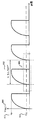
次に図2Aを参照して、図1のスイッチング電源の整流された電圧VRECT106の例示的な波形の図を図示する。これは、ハーフラインサイクル202、ゼロ交差電圧しきい値204、ピーク電圧VP205、および部分206を含む。図2Bは、例示的な整流された電圧VRECT106の部分206および対応のゼロ交差信号208を図示する。
2A, an exemplary waveform diagram of the rectified
一般的に、ac入力電圧VAC102は正弦波形であり、ac入力電圧VAC102の周期がフルラインサイクルと称される。数学的には、VAC(t)=VPsin(2πfLt)である。式中、VP205がac入力電圧VAC102のピーク電圧であり、fLがライン入力電圧の周波数である。または、換言すると、fLはac入力電圧VAC102のライン周波数である。フルラインサイクルはライン周波数fLの逆数である、または数学的にはフルラインサイクル=1/fLであることが認められるべきである。以上で言及したように、整流された電圧VRECT106は、ブリッジ整流器104への入力がac入力電圧VAC102である場合の、ブリッジ整流器104の結果的な出力である。図2Aに示される例示的な整流された電圧VRECT106については、ブリッジ整流器104は、ブリッジ整流器104の出力が正の大きさとなるように、または数学的にはVRECT=|VAC|=|VPsin(2πfLt)|となるように、ac入力電圧VAC102を変換した。その結果、整流された電圧VRECT106はハーフラインサイクル202をすべて繰返す。図2Aはゼロ交差電圧しきい値204も図示する。いくつかの実施例については、ゼロ交差電圧しきい値204は実質的に0に等しい。他の実施例については、ゼロ交差電圧204は、整流された電圧VRECT106のピーク電圧VP205の実質的に5分の1である。たとえば、整流された電圧VRECT106のピーク電圧VP205が実質的に125Vに等しい場合、ゼロ交差電圧しきい値204は実質的に25Vに等しい。ゼロ交差電圧しきい値VZC204の値がゼロ電圧に近づくにつれ、ゼロ交差信号208がより正確になることが認められるべきである。別の実施例では、ゼロ交差電圧204は、整流された電圧VRECT106のピーク電圧VP205の実質的に4分の1である。
Generally, the ac
図2Bは例示的な整流された電圧VRECT106の部分206および対応のゼロ交差信号208を図示する。コントローラ138は、ac入力電圧VAC102および整流された電圧VRECT106の値を間接的に検知してゼロ交差信号208を生成する。整流された電圧VRECT106がゼロ交差電圧しきい値204未満である場合、ゼロ交差信号208は、ゼロ交差条件が存在することを示す状態に変化する。ゼロ交差信号208は、整流された電圧VRECT106がゼロ交差電圧しきい値204を上回るまではその状態から変化しない。図2Bに示される例については、ゼロ交差信号208は、論理ハイおよび論理ローのセクションを有する矩形パルス波形である。整流された電圧VRECT106がゼロ交差電圧しきい値204未満である場合、ゼロ交差信号208の値は論理ハイである。整流された電圧VRECT106がゼロ交差電圧しきい値204を上回る場合、ゼロ交差信号208の値は論理ローである。ゼロ交差信号208がゼロ交差条件が存在すると示す時間の長さはゼロ交差パルス幅TZ210で示される。図2Bに示される例については、ゼロ交差パルス幅TZは、ゼロ交差信号208が論理ハイである時間の長さを示す。
FIG. 2B illustrates a
図2Aに示される整流された電圧VRECT106は、正の大きさまたは数学的にはVRECT=|VAC|=|VPsin(2πfLt)|であるac入力電圧VAC102である。整流された電圧VRECT106の値が0に近い電圧である場合は、ac入力電圧VAC102の値が交差ゼロ電圧、したがってゼロ交差という用語に近い場合に対応する。換言すると、整流された電圧VRECT106がいつ0に近い電圧であるかを検出することは、ac入力電圧VAC102がいつゼロ電圧と交差するかを検出することに対応する。図2Bに示されるように、整流された電圧VRECT106がゼロ交差電圧しきい値204未満である場合、ゼロ交差信号208はハイのパルスを出力し、コントローラ138にゼロ交差条件を示す。換言すると、−VZC<VAC(t)<VZCである場合、ゼロ交差信号208はハイのパルスを出力してゼロ交差条件を示す。本発明の実施例については、ac入力電圧VAC102のゼロ交差はスイッチ電流ID144を用いることによって間接的に検知される。
The rectified
図3にさまざまな動作モードのスイッチ電流を図示する。図1のスイッチモード電源の例示的なスイッチ電流波形の図を図示する。これは、スイッチング周期TS304、スイッチオン時間tON306、スイッチオフ時間tOFF308、台形310、および三角形312を含む。図3は、コントローラが連続導通モード(CCM)および不連続導通モード(DCM)の両方で動作している時間についてのスイッチ電流ID302の一般的な波形を図示する。スイッチ電流ID302の一般的な波形は、図1に図示されるスイッチ電流ID144の例を表わす。
FIG. 3 illustrates switch currents in various operating modes. 2 illustrates an example switch current waveform diagram of the switch mode power supply of FIG. This includes a
任意のスイッチング周期TS304の間、スイッチS1 114はコントローラ138からの駆動信号140に応答して導通し、出力量UOを調整し得る。スイッチング周期TS304は、スイッチオン時間tON306およびスイッチオフ時間tOFF308の2つの時間のセクションに分けられ得る。スイッチオン時間tON306は、スイッチS1 114が導通し得るスイッチング周期TS304の部分を示す。スイッチオフ時間tOFF308は、スイッチS1 114が導通することができないスイッチング周期TS304の残余の部分を示す。図3の電流波形は2つの基本的な動作モードを図示する。台形310は連続導通モード(CCM)の特徴である一方で、三角形312は不連続導通モード(DCM)の特徴である。CCMの間、スイッチ電流ID302は、スイッチオン時間tON306の開始直後は実質的に非ゼロである。DCMでは、スイッチ電流ID302は、スイッチオン時間tON306の開始直後は実質的にゼロである。スイッチオフ時間tOFF308の間、スイッチ電流ID302はCCMおよびDCMの両方について実質的にゼロである。本発明の実施例に従うスイッチング電源100は、CCMまたはDCMのいずれかで動作し得る。
During any
次に図4Aを参照して、例示的なスイッチ電流波形および結果的に生じるゼロ交差信号432の図を図示する。これは、スイッチ電流ID144、電流リミットILIM402、ゼロ交差電流しきい値IZC404、スイッチングサイクルT-2406からT8426、およびゼロ交差パルスTZ434を含む。図4Aは、電源100が不連続導通モード(DCM)で動作している時間に亘るスイッチ電流ID144の一般的な波形の一例を実証する。一般的に、スイッチングサイクルT-2406からT8426の各々はスイッチング周期TS304を有する。本発明のいくつかの実施例では、スイッチング周期TS304は一定の時間の長さであり得る。本発明の他の実施例では、コントローラ138はスイッチング周期TS304の長さを変えてもよい。
Referring now to FIG. 4A, a diagram of an exemplary switch current waveform and resulting zero
本発明の実施例については、コントローラ138は、スイッチ電流ID144を利用して、ac入力電圧VAC102がいつゼロ電圧と交差したかを判定する。図4Aは、いくつかのスイッチングサイクルT-2406からT8426に亘るスイッチ電流ID144の例を図示する。電流リミットILIM402は、スイッチS1 114について許される最大電流である。スイッチ電流ID144が電流リミットILIM402に達すれば、スイッチS1 114はスイッチングサイクルの残余の間オフする。スイッチ電流ID144がある時間量までにゼロ交差電流しきい値IZC404に達しない場合、可能なゼロ交差条件が存在し得る。
For an embodiment of the present invention,
Nは、コントローラ138がゼロ交差条件が確かに存在すると判定する前に可能なゼロ交差条件として検出する連続したスイッチングサイクルの数であり、ゼロ交差信号432は、非ゼロ交差条件を示す状態からゼロ交差条件を示す状態に変化することが認められるべきである。さらに、ゼロ交差信号432がゼロ交差条件が存在すると示している場合、コントローラはN個の連続スイッチングサイクル待機して、コントローラ138がゼロ交差信号432の状態を変化させる前にゼロ交差条件が存在しないと決定できるようにしてゼロ交差条件がないと示す。コントローラ138はN個の連続したスイッチングサイクル待機して、ゼロ交差条件の誤った検出に繋がり得る如何なるノイズリンギングもなくし得る。たとえば、Nが(図4Bに示されるように)4に等しい場合、コントローラ138は、可能なゼロ交差条件が4個の連続したスイッチングサイクルの間起こると、ゼロ交差条件が存在すると判定する。別の例では、Nが(図4Aに示されるように)1に等しい場合、コントローラ138は、可能なゼロ交差条件の最初の事象でゼロ交差条件が存在すると判定する。
N is the number of consecutive switching cycles that the
一実施例では、ゼロ交差信号432の論理ローの値はゼロ交差条件が存在しないことを示す一方で、ゼロ交差信号432の論理ハイの値はゼロ交差条件が存在することを示す。別の実施例では、ゼロ交差信号432の論理ハイの値はゼロ交差条件が存在しないことを示す一方で、ゼロ交差信号432の論理ローの値はゼロ交差信号が存在することを示す。
In one embodiment, a logic low value for zero
図4Aに示される例について、Nは1に等しく、コントローラ138は、可能なゼロ交差条件の最初の事象でゼロ交差条件が存在すると判定し、同じスイッチングサイクルの間にゼロ交差信号432の状態を変化させる。図4Aの例では、ゼロ交差信号432は、スイッチS1 114がオフし、スイッチ電流ID144がゼロ電流に降下すると、ゼロ交差条件を示す状態に変化する。スイッチングサイクルT-2406、T-1408、およびT0410で、スイッチ電流ID144はゼロ交差電流しきい値IZC404を超え、その結果コントローラ138はゼロ交差条件がないと検出する。図4Aの例については、ゼロ交差条件が存在しない場合、ゼロ交差信号432は論理ローの値である。しかしながら、スイッチングサイクルT1412で、スイッチ電流ID144は、ある時間量内でゼロ交差電流しきい値IZC404に達しない。Nは図4Aの例では1に等しいので、コントローラ138はac入力電圧VAC102についてゼロ交差条件が存在すると判定する。その結果、ゼロ交差信号432は、スイッチングサイクルT1412の間にゼロ交差条件を示す状態に変化する。図4Aの例については、ゼロ交差条件が存在する場合、ゼロ交差信号432は論理ハイの値である。
For the example shown in FIG. 4A, N is equal to 1, and
スイッチングサイクルT2414からT6422の間、スイッチ電流ID144は依然としてゼロ交差電流しきい値IZC404に達せず、コントローラ138はac入力電圧VAC102のゼロ交差条件が存在し続けていると判定する。その結果、ゼロ交差信号432は論理ハイの値に留まる。スイッチングサイクルT7424で、スイッチ電流ID144はゼロ交差電流しきい値IZC404を超え、コントローラ138はゼロ交差条件が存在しないと判定する。Nは1に等しいので、ゼロ交差信号432はスイッチングサイクルT7424の間に論理ローの値に変化する。図4Aの例については、ゼロ交差信号432は、スイッチS1 114がスイッチングサイクルT7424の間オフし、スイッチ電流ID144がゼロ電流に降下すると、非ゼロ交差条件を示す状態に変化する。図4Aに示されるように、ゼロ交差パルス幅TZ434は、ゼロ交差信号432がゼロ交差条件が存在し、論理ハイの値にあると示す時間の長さである。
During switching
次に図4Bを参照して、例示的なスイッチ電流波形および結果的に生じるゼロ交差信号432の別の図を図示する。これは、スイッチ電流ID144、電流リミットILIM402、ゼロ交差電流しきい値IZC404、スイッチングサイクルT0410からT10430、ゼロ交差パルス幅TZ434、および遅延時間tX436を含む。図4Bは、電源100がDCMで動作している時間に亘るスイッチ電流ID144の一般的な波形の一例を実証する。図4Bは図4Aに示される同じスイッチ電流ID144も図示するが、図4BについてはNが4に等しい。または、換言すると、コントローラ138は、ゼロ交差条件が確かに存在すると判定し、ゼロ交差信号432がゼロ交差条件を示す前に、可能なゼロ交差条件の後の4個の連続したスイッチングサイクル待機する。さらに、ゼロ交差信号432がゼロ交差条件が存在すると示す場合、コントローラ138は、コントローラ138がゼロ交差信号432の状態を変化させて非ゼロ交差条件を示す前に、非ゼロ交差条件で4個の連続したスイッチングサイクル待機する。コントローラ138は、4個の連続したスイッチングサイクルの間待機して、いずれのノイズリンギングもなくし、かつゼロ交差条件が確かに存在することを確実にする。図4BはNが4に等しいと図示するが、Nはいずれの正の整数であってもよい。
Referring now to FIG. 4B, another diagram of an exemplary switch current waveform and resulting zero
スイッチングサイクルT0410で、スイッチ電流ID144はゼロ交差電流しきい値IZC404を超え、その結果、コントローラ138はゼロ交差条件が存在すると判定せず、ゼロ交差信号432は論理ローの値に留まる。スイッチングサイクルT1412の間、スイッチ電流ID144はある時間量内でゼロ交差電流しきい値IZC404に達せず、コントローラ138は可能なゼロ交差条件が存在すると判定するが、ゼロ交差信号432は依然として論理ローの値に留まる。なぜなら、コントローラ138はゼロ交差条件が存在すると判定する前に可能なゼロ交差条件の4個の連続したスイッチングサイクル待機するからである。図4Bの例から、スイッチ電流ID144も、スイッチングサイクルT2414からT4418のある時間量内でゼロ交差電流しきい値IZC404に達しない。スイッチングサイクルT4418は、可能なゼロ交差条件が存在する4番目の連続したスイッチングサイクルである。したがって、コントローラ138は、ゼロ交差条件がac入力電圧VAC102について確かに存在すると判定し、ゼロ交差信号432は、ゼロ交差条件が存在すると示す状態に変化する。図4Bに示される例については、ゼロ交差信号432は、論理ローの値から論理ハイの値に遷移する。しかしながら、ゼロ交差信号432は遅延時間tX436の終わりまで論理ハイの値に遷移しない。遅延時間tX436は、コントローラ138がゼロ交差条件が確かに存在すると判定するのと、コントローラ138がゼロ交差信号432を更新するのとの間の時間の長さを示す。一実施例では、ゼロ交差信号が更新する遅延時間tX436は、数値Nを実現するのに用いられるフィルタによるものであり得る。さらなる実施例では、遅延時間tX436は次のスイッチングサイクルまでゼロ交差信号432の更新を遅延させ得る。図4Aに戻ると、遅延時間tX436は実質的に0に等しい。
At switching
スイッチングサイクルT5420およびT6422の間、スイッチ電流ID144は依然としてゼロ交差電流しきい値IZC404に達しておらず、コントローラはac入力電圧VAC102のゼロ交差条件が存在し続けていると判定し、ゼロ交差信号432は論理ハイの値に留まる。スイッチングサイクルT7424で、スイッチ電流ID144はac入力電圧VAC102のゼロ交差条件がもはや存在していない可能性があることを示すゼロ交差電流しきい値IZC404を超えるが、コントローラ138は、ac入力電圧VAC102がもはやゼロ交差条件にないと判定する前に、スイッチ電流ID144がゼロ交差条件がもはや存在しない可能性があることを示す4個の連続したスイッチングサイクル待機する。スイッチングサイクルT8426からT10430の間、スイッチ電流IDはゼロ交差電流しきい値IZC404を超える。スイッチングサイクルT10430は、ゼロ交差条件がもはや存在しない可能性がある4番目の連続したスイッチングサイクルであり、コントローラ138はゼロ交差条件が存在しないと判定する。その結果、ゼロ交差信号432は、ゼロ交差条件が存在しないと示す状態に変化する。図4Bに示される例については、ゼロ交差信号432は論理ハイの値から論理ローの値に遷移する。しかしながら、ゼロ交差信号432は、遅延時間tX436の終わりまで論理ローの値に遷移しない。遅延時間tX436は、コントローラ138がゼロ交差条件が存在しないことを判定するのと、コントローラ138がゼロ交差信号432を更新するのとの間の時間の長さを示す。さらなる実施例では、遅延時間tX436は、次のスイッチングサイクルまでゼロ交差信号432の更新を遅延させ得る。図4Bに示されるように、ゼロ交差パルス幅TZ434は、ゼロ交差信号432がゼロ交差条件が存在することを示し論理ハイの値にある時間の長さである。
During switching
次に図5を参照して、例示的なスイッチ電流波形および結果として生じるゼロ交差信号532の別の図を図示する。これは、スイッチ電流ID144、ゼロ交差電流しきい値IZC504、ゼロ交差時間しきい値tZC506、スイッチングサイクルTM508からTM+3514、およびゼロ交差パルス幅TZ534を含む。さらに、各々のスイッチングサイクルTM508からTM+3514の間に、スイッチS1 114のオン時間tONおよび延長されたオン時間tONXが存在する。一般的に、スイッチングサイクルTM508からTM+3514の各々はスイッチング周期TS304を有する。本発明のいくつかの実施例では、スイッチング周期TS304は一定の時間の長さであり得る。本発明の他の実施例では、コントローラ138はスイッチング周期TS304の長さを変え得る。図5に示される例示的なゼロ交差信号532については、Nの値は2である。
Referring now to FIG. 5, another diagram of an exemplary switch current waveform and resulting zero
一実施例では、コントローラ138は、スイッチS1 114のオン時間延長も利用して、ac入力電圧VAC102についてゼロ交差条件が存在するかどうかを判定する。コントローラ138は、スイッチ電流ID144がゼロ交差時間しきい値tZC506内にゼロ交差電流しきい値IZC504に達しない場合にゼロ交差条件が存在すると判定する。スイッチ電流ID144がスイッチS1 114の初期オン時間tONの間にゼロ交差電流しきい値IZC504に達しない場合、コントローラ138はゼロ交差電流しきい値IZC504に達するまでまたは延長されたオン時間tONXがゼロ交差時間しきい値tZC506に達するまで、オン時間tONを延長する。オン時間tONが延長される時間量は、延長されたオン時間tONXと称される。いくつかの実施例については、ゼロ交差時間しきい値tZC506は実質的に5μsに等しい。
In one embodiment,
スイッチングサイクルTM508で、スイッチ電流ID144は、スイッチS1 114の初期オン時間tON内にゼロ交差電流しきい値IZC504に達しない。スイッチS1 114をオフする代わりに、スイッチS1 114はオンのままであり、スイッチのオン時間tONは、スイッチ電流ID144がゼロ交差電流しきい値IZC504に達するまたはオン時間tONと延長されたオン時間tONXとの和がゼロ交差時間しきい値tZC506に達するまで、延長される。スイッチングサイクルTM508の間、オン時間tONは延長されたオン時間tONXだけ延長されるが、スイッチ電流ID144は、オン時間tONと延長されたオン時間tONXとの和がゼロ交差時間しきい値tZC506に達する前にゼロ交差電流しきい値IZC504に達する。その結果、スイッチS1 114は、スイッチ電流ID144がゼロ交差電流しきい値IZC504に達しスイッチ電流ID144が実質的に0に降下するときにオフされる。コントローラ138はゼロ交差条件を検出せず、その結果、ゼロ交差信号532は非ゼロ交差条件を示す。または、換言すると、ゼロ交差信号532は論理ローの値にある。
In switching
スイッチングサイクルTM+1510で、スイッチ電流ID144は初期オン時間tON内にゼロ交差電流しきい値IZC504に達せず、コントローラ138は延長されたオン時間tONXだけオン時間tONをさらに延長する。図示されるように、スイッチ電流ID144は延長されたオン時間tONXの間にゼロ交差電流しきい値IZC504に達する。スイッチングサイクルTM508とは異なり、スイッチ電流ID144は、オン時間tONと延長されたオン時間tONXとの和がゼロ交差時間しきい値tZC506に実質的に等しくなったときにゼロ交差電流しきい値IZC504に達する。コントローラ138はゼロ交差条件を検出せず、ゼロ交差信号532は論理ローの値に留まる。
In switching
スイッチングサイクルTM+2512で、スイッチ電流ID144は初期オン時間tON内にゼロ交差電流しきい値IZC504に達せず、コントローラ138は延長されたオン時間tONXだけオン時間tONをさらに延長する。以上で言及されたように、コントローラ138は、ゼロ交差時間しきい値tZC506に達しかつスイッチ電流ID144がゼロ交差電流しきい値IZC504未満であるときに、スイッチS1 114をオフする。図5に示される例では、スイッチ電流ID144は初期オン時間tON内にゼロ交差電流しきい値IZC504に達せず、コントローラ138はスイッチS1 114のオン時間を延長する。オン時間tONは、スイッチ電流ID144がゼロ交差電流しきい値IZC504に達するまでまたは延長されたオン時間tONXがゼロ交差時間しきい値tZC506に達するまで延長される。スイッチングサイクルTM+2512の間に、延長されたオン時間tONXは、スイッチ電流144がゼロ交差電流しきい値IZC504に達しないうちにゼロ交差時間しきい値tZC506に達する。その結果、コントローラ138は可能なゼロ交差条件が存在し得ると判定するが、ゼロ交差信号532は状態を変化させない。なぜなら、コントローラ138は、ゼロ交差条件が存在すると判定する前に可能なゼロ交差条件の2つの連続するスイッチングサイクル待機するからである。換言すると、Nが2に等しいので、ゼロ交差信号532は論理ハイの値に遷移しない。
In switching
スイッチングサイクルTM+3514で、スイッチ電流ID144は初期オン時間tON内にゼロ交差電流しきい値IZC504に達せず、コントローラ138は延長されたオン時間tONXだけオン時間tONをさらに延長する。スイッチングサイクルTM+2512と同様に、スイッチ電流ID144は、延長されたオン時間tONXがゼロ交差時間しきい値tZC506に達する前にゼロ交差電流しきい値IZC504に達しない。さらに、スイッチングサイクルTM+3514は、可能なゼロ交差条件を有する2番目の連続したスイッチングサイクルである。その結果、コントローラ138はゼロ交差条件が存在すると判定し、ゼロ交差信号532は状態を変化させる。または、換言すると、ゼロ交差信号432は論理ハイの値に遷移する。ゼロ交差パルス幅TZ534は、ゼロ交差信号532が論理ハイの値にある時間量を示す。
In switching
ゼロ交差電流しきい値IZC504およびゼロ交差時間しきい値tZC506は、ゼロ交差電圧しきい値VZC204に対応するように選択される。以上で言及されたように、コントローラ138は、スイッチ電流ID144がゼロ交差時間しきい値tZC506までにゼロ交差電流しきい値IZC504に達しないときにゼロ交差条件を検出する。ゼロ交差電流しきい値IZC504およびゼロ交差時間しきい値tZC506は、ゼロ交差条件が、ゼロ交差電圧しきい値VZC204を下回る、整流された電圧VRECT106の値に対応するように固定される。換言すると、ゼロ交差電流しきい値IZC504およびゼロ交差時間しきい値tZC506は、ゼロ交差条件が正のゼロ交差電圧しきい値VZC204と負のゼロ交差電圧しきい値VZC204との間に降下するac入力電圧VAC102の値、または数学的には−VZC<VAC(t)<VZC、に対応するように固定される。
Zero crossing current threshold I ZC 504 and zero crossing
スイッチS1 114がオンであるときのスイッチS1 114の電圧と電流との間の関係は
The relationship between the voltage and current of

として表現され得る。式中、LPが1次巻線110のインダクタンスである。DCMで動作する電源については、いずれのスイッチングサイクルの間のこの関係も Can be expressed as In the equation, L P is the inductance of the primary winding 110. For power supplies operating in DCM, this relationship between any switching cycles
としてさらに表わされ得る。式中、IPEAKはスイッチ電流ID144のピーク値である。しかしながら、1つのスイッチングサイクルにおいては、VACの値は、オン時間tONが小さいために一定であると考えられ得る。以上で言及されたように、ゼロ交差電流しきい値IZC504およびゼロ交差時間しきい値tZC506は、スイッチS1 114がDCMでオンであるときのスイッチS1 114の電圧と電流との間の関係、または数学的には
Can be further represented as Where I PEAK is the peak value of the switch
を利用して、ゼロ交差電圧しきい値VZC204に対応するように固定され選択される。
さらに、ゼロ交差時間しきい値tZC506を固定するようにコントローラ138が利用するオン時間延長により、フィルタコンデンサCF120からより多くの電荷が除去される。その結果、放電するフィルタコンデンサCF120は、コントローラ138がac入力電圧VAC102のゼロ交差を検出するのを助け得る1次巻線110における電圧をプルダウンするのを助ける。
Is fixed and selected to correspond to the zero-crossing
Furthermore, the on-time extension utilized by
次に図6を参照して、調光器回路608を利用する例示的なスイッチング電源の機能ブロック図を示す。これは、ac入力電圧VAC102、エネルギ転送要素T1 108、エネルギ転送要素T1 108の1次巻線110、エネルギ転送要素T1 108の2次巻線112、スイッチS1 114、入力帰還116、クランプ回路118、フィルタコンデンサCF120、コントローラ138、駆動信号140、電流検知入力信号142、およびスイッチ電流ID144を含む。さらに、スイッチング電源は、整流器604、整流された電圧VRECT606、調光器回路608、および調光された電圧VDIM610をさらに含む。図6に示されるスイッチング電源は、図1に示されるスイッチング電源100に調光器回路608が追加されたものと同様であることが認められるべきである。
With reference now to FIG. 6, a functional block diagram of an exemplary switching power supply utilizing a
エネルギ転送要素T1 108、エネルギ転送要素T1 108の1次巻線110、エネルギ転送要素T1 108の2次巻線112、スイッチS1 114、入力帰還116、クランプ回路118、フィルタコンデンサCF120、コントローラ138、駆動信号140、電流検知入力信号142、およびスイッチ電流ID144は上述のように結合しかつ機能する。調光器回路608はac入力電圧VAC102に結合し、調光された電圧VDIM610を生成する。調光器回路608は整流器604にさらに結合する。整流器604は調光された電圧VDIM610を受け、整流された電圧VRECT606を出力する。図6に示されるように、整流器604はフィルタコンデンサCF120の両端に結合される。本発明のいくつかの実施例については、整流器604は図1に図示されるようなブリッジ整流器である。
Energy
調光器回路608は、電源の負荷126が発光ダイオード(LED)アレイである場合に利用され、電源に送達される電力の量を制限し得る。その結果、LEDアレイである負荷に送達される電流が制限され、LEDアレイが薄暗くなる。一実施例では、調光器回路608は位相調光器回路である。別の実施例では、トライアック調光器回路が調光器回路608として利用され得る。トライアック調光器は、ac入力電圧VAC102がゼロ電圧と交差する際に、電源からac入力電圧VAC102を切り離す。所与の時間量の後、トライアック調光器は、電源にac入力電圧VAC102を再接続する。求められる調光量に依存して、トライアック調光器は、ac入力電圧VAC102が電源から切り離される時間量を制御する。一般的に、より多くの調光は、トライアック調光器がac入力電圧VAC102を切り離すより長い期間に対応する。本発明の実施例に従うと、コントローラ138はスイッチ電流ID144を利用して、ac入力電圧VAC102についていつゼロ交差条件が存在するかを判定し、ゼロ交差信号を生成する。図7Aおよび図7Bは、整流された電圧VRECT606およびその後のゼロ交差信号を図示する。
The
図7Aは、図6に示される整流された電圧VRECT606の例示的な波形を図示し、これは、ハーフラインサイクル702、ゼロ交差電圧しきい値704、ピーク電圧VP705、および部分706を含む。図7Bは、整流された電圧VRECT606の部分706および対応のゼロ交差信号708を図示する。ハーフラインサイクル702、ゼロ交差電圧しきい値VZC704、およびゼロ交差信号708は、図2Aおよび図2Bのハーフラインサイクル202、ゼロ交差電圧しきい値VZC204、およびゼロ交差信号208のさらなる例である。
FIG. 7A illustrates an exemplary waveform of the rectified
以上論じたように、ac入力電圧VAC102は、フルラインサイクルと称されるac入力電圧VAC102の周期の正弦波形である。数学的にはVAC(t)=VPsin(2πfLt)である。式中、VP705はac入力電圧VAC102のピーク電圧であり、fLはライン入力電圧の周波数である。または、換言すると、fLはac入力電圧VAC102のライン周波数である。フルラインサイクルはライン周波数fLの逆数であり、または数学的にはフルラインサイクル=1/fLであることが認められるべきである。整流された電圧VRECT606は、ブリッジ整流器604および調光回路608の結果的な出力である。図7Aの例については、整流された電圧VRECT606の各々のハーフラインサイクル702の開始は、調光器回路608がac入力電圧VAC102を電源から切り離すときに対応するゼロ電圧に実質的に等しい。調光器回路608がac入力電圧VAC102を電源に再接続する際、整流された電圧VRECT606はac入力電圧VAC102の正の大きさに実質的に従う。または、数学的にはVRECT=|VDIM|である。
As discussed above, the ac
図2Aと同様に、いくつかの実施例については、ゼロ交差電圧しきい値VZC704は実質的に0に等しい。他の実施例については、ゼロ交差電圧しきい値VZC704は、整流された電圧VRECT606のピーク電圧VP705の実質的に5分の1である。一例では、整流された電圧VRECT606のピーク電圧VP705が125Vに実質的に等しい場合、ゼロ交差電圧しきい値VZC704は実質的に25Vに等しい。別の実施例では、ゼロ交差電圧しきい値VZC704は、整流された電圧VRECT606のピーク電圧VP705の実質的に4分の1である。ゼロ交差電圧しきい値VZC704の値がゼロ電圧に近づくにつれ、ゼロ交差信号708がより正確になることが認められるべきである。
Similar to FIG. 2A, for some embodiments, the zero-crossing
図7Bは、整流された電圧VRECT606の部分706および対応のゼロ交差信号708を図示する。本発明の実施例は、ac入力電圧VAC102を間接的に検知し、ゼロ交差信号708を生成する。整流された電圧VRECT606がゼロ交差電圧しきい値VZC704未満である場合、ゼロ交差信号708はゼロ交差条件が存在すると示す。ゼロ交差信号708は、論理ハイおよび論理ローのセクションを有する矩形パルス波形である。図7Bに図示される例については、整流された電圧VRECT606がゼロ交差電圧しきい値VZC704未満である場合、ゼロ交差信号708の値は論理ハイである。整流された電圧VRECT606がゼロ交差電圧しきい値VZC704よりも大きい場合、ゼロ交差信号708の値は論理ローである。
FIG. 7B illustrates a
図2Bについて以上で言及されたように、整流された電圧VRECT606がいつゼロ電圧に近いかを検出することは、ac入力電圧VAC102がいつゼロ電圧と交差するかを検出することに対応する。図7Bに示されるゼロ交差信号708と図2Bに示されるゼロ交差信号208とを比較すると、図7Bのゼロ交差パルスTZ710は、調光器回路608によるac入力電圧VAC102の切り離しのために、図2Bのゼロ交差パルスTZ210よりも長くなっている。以上で言及されたように、求められる調光量は、調光器回路608が電源からac入力電圧VAC102を切り離す時間の長さに対応する。調光器回路608がac入力電圧VAC102を電源から切り離した状態に保つ時間が長いほど、整流された電圧VRECT606が実質的にゼロ電圧に等しい時間が長くなる。その結果、ゼロ交差パルスTZ710の長さは、調光器回路608が与える調光量に対応する。
As noted above for FIG. 2B, detecting when the rectified
次に図8Aを参照して、整流された電圧VRECT801の別の例示的な波形を図示する。これは、ハーフラインサイクル802、ゼロ交差電圧しきい値VZC804、ピーク電圧VP805、および部分806を含む。図8Bは、整流された電圧VRECT801の部分806および対応のゼロ交差信号808を図示する。
Referring now to FIG. 8A, another exemplary waveform of the rectified
整流された電圧VRECT801の例示的な波形は、図7Aに示される整流された電圧VRECT606と同様である。図7Aの例では、整流された電圧VRECT606は、調光器回路608および整流器604を通過したac入力電圧VAC102の結果である。図6、図7Aおよび図7Bに関して言及したように、整流された電圧VRECT606は、すべてのハーフラインサイクル802の開始時にac入力電圧VAC102を切り離すトライアック調光器などの調光器回路608の結果である。しかしながら、図8Aおよび図8Bに図示される整流された電圧VRECT801は、すべてのハーフラインサイクル802の終わりにac入力電圧VAC102を切り離す調光器回路608の結果である。その結果、整流された電圧VRECT801は、ハーフラインサイクル802の終わりにゼロ電圧に実質的に等しくなる。ハーフラインサイクル802の開始時に、整流された電圧VRECT801は、調光器回路608が電源からac入力電圧VAC102を切り離すまで、ac入力電圧VAC102の正の大きさに実質的に従う。整流された電圧VRECT801の値は次に、次のハーフラインサイクルの開始時まで、実質的にゼロ電圧まで放電する。
An exemplary waveform of the rectified
図8Bは整流された電圧VRECT801の部分806および対応のゼロ交差信号808を図示する。ac入力電圧VAC102は、スイッチ電流ID144を通して間接的に検知されてゼロ交差信号808を生成する。整流された電圧VRECT801がゼロ交差電圧しきい値VZC804未満である場合、ゼロ交差信号808はゼロ交差条件が存在すると示す。図8Bの例については、整流された電圧VRECT801がゼロ交差電圧しきい値VZC804未満である場合、ゼロ交差信号808の値は論理ハイである。整流された電圧VRECT801がゼロ交差電圧しきい値VZC804よりも大きい場合、ゼロ交差信号808の値は論理ローである。
FIG. 8B illustrates a
図8Bに示されるゼロ交差信号808と図2Bに示されるゼロ交差信号208とを比較すると、図8Bのゼロ交差パルスTZ810は、調光器回路608によるac入力電圧VAC102の切り離しにより、図2Bのゼロ交差パルスTZ210よりも長くなっている。図8Bに示されるゼロ交差信号808と図7Bに示されるゼロ交差信号708とを比較すると、図8Bのゼロ交差パルスTZ810は、図7Bに示されるようなハーフラインサイクル802の開始時ではなく、ハーフラインサイクル802の終わりに向けて生じる。
Comparing the zero-
次に図9Aを参照して、コントローラ938の機能ブロック図を図示する。これは、フィードバック信号UFB930、駆動信号940、電流検知信号942、駆動論理ブロック902、オン時間延長ブロック904、ゼロ交差検出器906、ゼロ交差信号908、およびゼロ交差時間しきい値パルスZCP924を含む。ゼロ交差検出器906は、クロック信号910、比較器914、参照信号916、ANDゲート917、S−Rラッチ918、フリップフロップ922、およびオプションのゼロ交差フィルタ926をさらに含む。コントローラ938、フィードバック信号UFB930、駆動信号940、および電流検知信号942は、図1および図6に図示されるコントローラ138、フィードバック信号UFB130、駆動信号140、および電流検知信号142の例である。さらに、ゼロ交差信号908は、図2、図4A、図4B、図7B、および図8Bに示されるゼロ交差信号の一例である。一例では、駆動論理ブロック902およびオン時間延長ブロック904は本明細書中では駆動信号生成器と総称され得る。駆動論理出力DLO950、ゼロ交差時間しきい値パルスZCP924、および比較器出力CO952という信号表記も図9Aおよび図9Bに示される。それぞれの信号の波形は図10に図示する。
Referring now to FIG. 9A, a functional block diagram of the
コントローラ938、フィードバック信号UFB930、駆動信号940、および電流検知信号942は上述のように結合しかつ機能する。コントローラ938内では、駆動論理ブロック902は、オン時間延長ブロック904およびゼロ交差検出器906に結合する。駆動論理ブロック902は電流検知信号942およびフィードバック信号UFB930を受け、オン時間延長ブロック904へ駆動論理出力DLO950を出力する。駆動論理ブロック902はゼロ交差検出器906にさらに結合し、ゼロ交差信号908を受ける。ゼロ交差検出器906は電流検知信号942に結合しかつこれを受ける。さらに説明されるように、ゼロ交差検出器906は電流検知信号942を受け、駆動論理ブロック902にゼロ交差信号908を出力する。
駆動論理ブロック902はフィードバック信号UFB930、電流検知信号942およびゼロ交差信号908を利用して、駆動信号940の状態およびコントローラ938の状態に関する情報をオン時間延長ブロック904に与える駆動論理出力信号DLO950を生成する。オン時間延長ブロック904はゼロ交差検出器906にさらに結合し、本明細書中では比較器出力CO952と称される比較器914の出力を受ける。さらに、オン時間延長ブロック904はゼロ交差時間しきい値パルスZCP924を受ける。ゼロ交差時間しきい値パルスZCP924は、論理ハイおよび論理ローのセクションの長さが変化する矩形パルス波形である。論理ローのセクションの長さはゼロ交差時間しきい値tZC506に実質的に等しく、ゼロ交差時間しきい値パルスZCP924の連続した立下がりエッジ同士の間の時間の長さはスイッチング周期TSに実質的に等しい。
Drive
オン時間延長ブロック904は、受けた駆動論理出力DLO950、ゼロ交差時間しきい値パルスZCP924および比較器出力CO952を利用して、駆動信号940を出力する。以上で言及されたように、駆動信号940は、電源のスイッチ(たとえば図1のスイッチS1 114)のスイッチングを制御するのに利用される。ゼロ交差検出器906のフリップフロップ922も駆動信号940を受ける。さらに、オン時間延長ブロック904は、図5に関して論じたオン時間延長を実現する。
The on-
駆動論理ブロック902は、電流検知信号942からのスイッチ電流ID144に関する情報およびフィードバック信号UFB930からの出力量UOに関する情報を、ゼロ交差信号908とともに受ける。この情報を利用して、駆動論理ブロック902は、意図される駆動信号に関する情報を与えて、スイッチS1 114のオンおよびオフを制御する。一例では、駆動論理ブロック902は電流検知信号942を利用して、図4Aおよび図4Bに関して論じられたようにいつスイッチ電流ID144が電流リミットILIM402に達して、スイッチS1 114をオフするかを判定し得る。オン時間延長ブロック904は、比較器出力CO952およびゼロ交差時間しきい値パルスZCP924とともに、駆動論理出力DLO950を受ける。さらに論じられるように、比較器出力CO952およびゼロ交差時間しきい値パルスZCP924の値に依存して、オン時間延長ブロック904は、駆動論理ブロック902が与える意図される駆動信号のオン時間を延長し得る。
The
ゼロ交差検出器906は、電流検知信号942および参照信号916を受ける比較器914をさらに含む。図9Aの例では、比較器914は、比較器914の非反転入力で電流検知信号942を受け、比較器914の反転入力で参照信号916を受ける。このように、一実施例では、電流検知信号942が参照信号916未満であることがゼロ交差条件の存在を示し得る。電流検知信号942および参照信号916は電流信号または電圧信号であり得る。電流検知信号942はスイッチ電流ID144に関する情報を与える。電流検知信号942が電流信号である場合、参照信号916はゼロ交差電流しきい値IZC404であり得、比較器914は電流比較器である。以上で言及されたように、スイッチ電流ID144は、たとえば個別の抵抗器の両端の電圧またはトランジスタが導通しているときのトランジスタの両端の電圧などのさまざまな態様で検知され得る。それらの例については、電流検知信号942は電圧信号である。電流検知信号942が電圧信号である場合、参照信号916は参照電圧であり、比較器914は電圧比較器である。
Zero
比較器914はANDゲート917およびオン時間延長ブロック904にさらに結合される。比較器914の出力はオン時間延長ブロック904によって受けられる。ANDゲート917はゼロ交差時間しきい値パルスZCP924を受けるようにも結合される。比較器出力CO952を受けるANDゲート917の入力に結合される丸印は、ANDゲート917が反転された比較器出力CO952を受けるように、比較器914とANDゲート917との間に反転器が結合されることを示す。たとえば、ANDゲート917の出力は、ゼロ交差時間しきい値パルスZCP924が論理ハイの値にありかつ比較器出力CO952が(論理ハイの値にある反転された比較器出力CO952に対応する)論理ローの値にある場合、論理ハイの値にある。
S−Rラッチ918は、本明細書中ではS−Rラッチ918のR入力とも称されるリセット入力でANDゲート917の出力を受ける。さらに、S−Rラッチ918は、本明細書中ではS入力とも称されるセット入力でクロック信号910を受ける。クロック信号910はスイッチング周期TSに関する情報を与え、いくつかの実施例では、発振器(図示せず)から入来し得る。クロック信号910は、論理ハイおよび論理ローのセクションの長さが変化する矩形のパルス信号である。クロック信号910の連続した立上がりエッジ同士の間の時間の長さがスイッチング周期TSに実質的に等しい。クロック信号910が一旦論理ハイの値のパルスを出力すると、クロック信号910は論理ローの値に素早く立下がる。このように、S−Rラッチ918はクロック信号910の立上がりエッジでセットされる。しかしながら、S−Rラッチ918は、ANDゲート917の出力が論理ハイの値にあるとリセットする。換言すると、電流検知信号942によって与えられるスイッチ電流ID144が参照信号916によって与えられるゼロ交差電流しきい値IZC404を超えたことを比較器出力CO952が示すと、ラッチ918はリセットする。図9Aの例では、S−Rラッチ918の出力はQバー出力から取得される。このように、S−Rラッチ918がセットされると、S−Rラッチ918の出力は論理ローの値である。S−Rラッチ918がリセットされると、S−Rラッチの出力は論理ハイの値である。
The
フリップフロップ922はS−Rラッチ918に結合し、S−Rラッチ918の出力を受ける。一実施例では、フリップフロップ922はDフリップフロップである。フリップフロップ922はD入力でラッチ918の出力を受ける。さらに、フリップフロップ922はクロック入力で駆動信号940を受ける。駆動信号940は、論理ハイおよび論理ローのセクションの長さが変化する矩形パルス波形である。一実施例では、閉じている(すなわちオンの)スイッチS1 114は駆動信号940の論理ハイの値に対応する一方で、開いている(すなわちオフの)スイッチS1 114は駆動信号940の論理ローの値に対応する。フリップフロップ922のクロック入力に結合された丸印は、フリップフロップ922が駆動信号940の立下がりエッジで更新することを示す。換言すると、フリップフロップ922の出力は、スイッチS1 114がオフするときに更新する。フリップフロップ922はゼロ交差フィルタ926にさらに結合される。図示されるように、ゼロ交差フィルタ926はフリップフロップ922の出力を受け、ゼロ交差信号908を出力する。フリップフロップ922の出力はゼロ交差信号908に実質的に等しいが、ゼロ交差フィルタ926は、フリップフロップ922の出力のノイズを低減するように結合される。さらに、ゼロ交差フィルタ926は、N個の連続したスイッチングサイクルが可能なゼロ交差条件を有していなければゼロ交差条件が存在すると、ゼロ交差信号908が示さないように、以上で論じたように数Nを実現する。しかしながら、Nが1に等しい場合は、ゼロ交差フィルタ926はゼロ交差検出器906から省略されてもよい。
Flip-
スイッチング周期TSの開始時に電流検知信号942は参照信号916未満であり、したがって比較器914の出力は論理ローである。換言すると、スイッチング周期TSの開始時に、スイッチ電流ID144はゼロ交差電流しきい値IZC404未満である。クロック信号910は、スイッチング周期TSの開始時に論理ハイの値のパルスを出力し、S−Rラッチ918の出力は論理ローの値にセットされる。クロック信号910は迅速に論理ローの値のパルスを出力し、S−Rラッチ918は以前の値を保持する。この例については、S−Rラッチ918は論理ローの値を保持する。
At the beginning of the switching period T S , the
フリップフロップ922はスイッチS1 114が開く(すなわちオフになる)と更新する。換言すると、フリップフロップ922は、フリップフロップ922の出力を更新して、駆動信号940の立下がりエッジでフリップフロップ922のD入力を反映する。一般的に、Dフリップフロップはクロック入力の立上がりエッジで更新する。しかしながら、フリップフロップ922のクロック入力における丸印が反転器を示す場合、フリップフロップ922は駆動信号940の立下がりエッジで更新する。
Flip-
電流検知信号942が与えるスイッチ電流ID144が、ゼロ交差時間しきい値パルスZCP924が与えるゼロ交差時間しきい値TM+3に達する前に(または換言すると、ゼロ交差時間しきい値パルスZCP924が論理ハイの値に遷移する前に)参照信号916が与えるゼロ交差電流しきい値IZC404を超えなければゼロ交差条件が検出され、ANDゲート917の出力は論理ハイの値である。ANDゲート917の論理ハイの出力はS−Rラッチ918をリセットし、S−Rラッチ918の出力は論理ハイの値である。駆動信号940の立下がりエッジでフリップフロップ922が更新し、フリップフロップ922の出力はS−Rラッチ918の論理ハイの出力を転送する。一例では、フリップフロップ922の出力はゼロ交差フィルタ926によってフィルタリングされ、結果的に得られるゼロ交差信号908は論理ハイの値である。一実施例では、ゼロ交差フィルタ926の出力は、図4Bに関して論じられたように、遅延時間tX436の後で更新される。別の実施例では、ゼロ交差フィルタ926の出力は次のスイッチングサイクルで更新される。さらに、ゼロ交差フィルタ926は、ゼロ交差検出器906がゼロ交差条件が存在すると決定する前に可能なゼロ交差条件を有するN個の連続したスイッチングサイクルを実現してもよい。一実施例では、ゼロ交差フィルタ926は、フリップフロップ922の出力が論理ハイの値である連続したスイッチングサイクルの数を数える論理回路を含んでもよい。このように、一実施例では、ゼロ交差フィルタ926は、図4Bを参照して上述されたように、N回の可能なゼロ交差条件が生じた後でのみゼロ交差条件の存在を示すゼロ交差信号908を出力してもよい。一実施例では、ゼロ交差フィルタ926はフリップフロップおよびマルチプレクサを利用して数Nを実現してもよい。別の実施例では、ゼロ交差フィルタ926はカウンタを利用して数Nを実現してもよい。いくつかの実施例では、図4Bに関して論じられた遅延時間tX436は、ゼロ交差フィルタ926に利用される要素によるものであってもよい。
Before the switch current I D 144 provided by the
電流検知信号942によって与えられるスイッチ電流ID144が、ゼロ交差時間しきい値パルスZCP924によって与えられるゼロ交差時間しきい値tZCに達する前に(または換言すると、ゼロ交差時間しきい値パルスZCP924が論理ハイの値に遷移する前に)参照信号916が与えるゼロ交差電流しきい値IZC404を超えるとゼロ交差条件が検出されず、ANDゲート917の出力は論理ローの値である。S−Rラッチ918はリセットされず、S−Rラッチ918の論理ローの値は駆動信号940の立下がりエッジでフリップフロップ922の出力に転送される。一例では、フリップフロップ922の出力はゼロ交差フィルタ926によってフィルタリングされ、結果的に得られるゼロ交差信号908は論理ローの値にある。一実施例では、ゼロ交差フィルタ926は、図4Bに関して論じられたように、遅延時間tX436の後にその出力を更新する。別の実施例では、ゼロ交差フィルタ926の出力は次のスイッチングサイクルで更新される。さらに、ゼロ交差フィルタ926は、ゼロ交差検出器906がゼロ交差条件がもはや存在しないと決定する前に非ゼロ交差条件を有するN個の連続したスイッチングサイクルを実現してもよい。たとえば、ゼロ交差フィルタ926は、フリップフロップ922の出力が論理ローの値である連続したスイッチングサイクルの数を数える論理回路を含んでもよい。このように、一実施例では、ゼロ交差フィルタ926は、図4Bを参照して上述されたように、非ゼロ交差条件を有するN個のスイッチングサイクルの後でのみ、ゼロ交差条件がもはや存在しないことを示すゼロ交差信号908を出力してもよい。
Before the switch current I D 144 provided by the
次に図9Bを参照して、オン時間延長ブロック904のブロック図を図示する。これは、ゼロ交差時間しきい値パルスZCP924、駆動信号940、駆動論理出力DLO950、比較器出力CO952、オプションの単安定マルチバイブレータ954、反転器964、S−Rラッチ958、ORゲート960、立下がりエッジ遅延961、およびANDゲート968を含む。さらに、図9Bは、信号表記A 962、B 970、C 956、および反転された駆動論理出力
Referring now to FIG. 9B, a block diagram of the on
![]()
![]()
を図示する。それぞれの信号の波形は図10に図示する。
ゼロ交差時間しきい値パルスZCP924、駆動信号940、駆動論理出力DLO950、および比較器出力CO952は上述のように結合しかつ機能する。さらに、オン時間延長ブロック904は、任意的に、駆動論理出力DLO950に結合しかつこれを受ける単安定マルチバイブレータ954を含んでもよい。上述のように、駆動論理出力DLO950は、コントローラの状態に関する情報および意図される駆動信号をオン時間延長ブロック904に与える。駆動論理出力DLO950は、論理ハイおよび論理ローのセクションの長さが変化する矩形パルス波形であり、連続した立上がりエッジ同士の間の時間の長さがスイッチング周期TSに実質的に等しい。単安定マルチバイブレータ954は駆動論理出力DLO950を受け、駆動論理出力DLO950の毎立上がりエッジにパルスを生成する。一実施例では、単安定マルチバイブレータ954が生成するパルスの幅は実質的に50ナノ秒(ns)に等しい。単安定マルチバイブレータ954の出力は信号C 956と表記され、その例示的な波形が波形C 1056として図10に図示される。単安定マルチバイブレータ954はS−Rラッチ958に結合する。図9Bに示される例については、単安定マルチバイブレータ954はS−Rラッチ958のS入力に結合する。S−Rラッチ958は、S入力で単安定マルチバイブレータ954の出力である信号C 956を受ける。別の実施例では、信号C 956は発振器(図示せず)によって生成されてもよい。
Is illustrated. The waveform of each signal is illustrated in FIG.
Zero crossing time
さらに、オン時間延長ブロック904は比較器出力952およびゼロ交差時間しきい値パルスZCP924に結合する。遅延時間tDだけ比較器出力952の立下がりエッジを遅延させる立下がりエッジ遅延961が比較器出力952を受ける。立下がりエッジ遅延961はORゲート960にさらに結合し、ORゲート960の一方の入力で信号COと表記される立下がりエッジ遅延961の出力を受ける。ORゲート960の他方の入力はゼロ交差時間しきい値パルスZCP924を受ける。ORゲート960はANDゲート968にさらに結合し、ANDゲート968の一方の入力が信号A 962と表記されるORゲート960の出力を受ける。
In addition, on
さらに、ANDゲート968も反転器964に結合する。反転器964は駆動論理出力DLO950に結合しかつこれを受ける。反転された駆動論理出力
In addition, AND
![]()
![]()
が反転器964から出力され、ANDゲート968がこれを受ける。ANDゲート968はS−Rラッチ958のR入力にさらに結合する。S−Rラッチ958のR入力が信号B 970と表記されるANDゲート968の出力を受ける。S−Rラッチ958はS入力およびR入力での値を利用して駆動信号940を出力する。
Is output from the
図9Bに示されるように、比較器出力CO952が、スイッチ電流ID144がゼロ交差電流しきい値IZC未満であると示す場合、ORゲート960の出力は、ANDゲート968がS−Rラッチ958をリセットしないようにし得る。換言すると、比較器出力CO952が、スイッチ電流ID144がゼロ交差電流しきい値IZC未満であると示す場合、ORゲート960の出力は、S−Rラッチ958が論理ローの値を出力しないようにし、こうしてスイッチS1 114のオン時間を延長し得る。図10にさらに図示されるように、ORゲート960の出力はS−Rラッチ958がリセットしないようにし、こうして比較器出力CO952が、スイッチ電流ID144がゼロ交差電流しきい値IZCに達したと示すか、またはゼロ交差時間電流しきい値ZCP924がゼロ交差時間しきい値tZCに達したと示すまで、スイッチS1 114のオン時間を延長する。しかしながら、スイッチ電流ID144が、駆動論理出力DLO950が与える初期スイッチオン時間の間にゼロ交差電流しきい値IZCを超えれば、または換言すると駆動論理出力DLO950が論理ハイの値にある場合、S−Rラッチ958は駆動論理出力DLO950の立下がりエッジでリセットする。なぜなら、駆動論理出力DLO950は、意図される駆動信号に関する情報を与えるからである。図9Aおよび図9Bに関して論じた信号のさまざまな波形を図10に図示する。
As shown in FIG. 9B, if the comparator output CO952 indicates that the switch current I D 144 is less than the zero-crossing current threshold I ZC , the output of the
次に図10を参照して、図9Aおよび図9Bに対応するさまざまな波形を図示する。図10は、コントローラ938およびゼロ交差検出のためのオン時間延長を実現するオン時間延長ブロック904のさまざまな波形同士の間の差を図示する。例示的な波形ID1044、DLO1050、
Referring now to FIG. 10, various waveforms corresponding to FIGS. 9A and 9B are illustrated. FIG. 10 illustrates the difference between the various waveforms of the
![]()
![]()
、CO1052、ZCP1024、A 1062、B 1070、C 1056、および駆動信号1040は、スイッチ電流ID144、駆動論理出力DLO950、反転器駆動論理出力
, CO 1052,
![]()
![]()
、立下がりエッジ遅延比較器出力CO、ゼロ交差時間電流しきい値ZCP924、ならびに信号表記A 962、B 970、C 956、および駆動信号940に対応する。さらに、図10は、スイッチングサイクル1002、1004、および1006を図示する。図示されるように、各々のスイッチングサイクルはスイッチング周期TSを有する。
, Falling edge delay comparator output CO, zero crossing time
図10に示される例については、すべてのスイッチングサイクルの開始時に、駆動論理出力DLO1050は論理ハイの値にある。さらに、スイッチ電流ID1044がゼロ交差電流しきい値IZC未満であるため、比較器出力CO1052は論理ローの値にある。ゼロ交差時間しきい値パルスZCP1024は、すべてのスイッチングサイクルの開始時に論理ローの値にある。ORゲート960の出力である波形A 1062は論理ローの値にある。ANDゲート968は波形A 1062の論理ローの値および(現在は論理ローの値にある)反転された駆動論理出力
For the example shown in FIG. 10, at the beginning of every switching cycle, the drive
![]()
![]()
を受け、その結果、波形B 1070はすべてのスイッチングサイクルの開始時に論理ローの値である。単安定マルチバイブレータ954は駆動論理出力DLO1050を受け、波形C 1056で示される論理ハイのパルスを出力する。すべてのスイッチングサイクルの開始時に波形C 1056は論理ハイの値にある一方で、波形B 1070は論理ローの値にある。その結果、S−Rラッチ958は論理ハイの値にある駆動信号1040を出力し、スイッチS1 114がオンし、スイッチ電流ID1044が増加し始める。波形C 1056は論理ローの値に迅速に立下がり、S−Rラッチ958は以前の値を保持する。すべてのスイッチングサイクルの開始時に、S−Rラッチ958は論理ハイの値を保持し、スイッチS1 114はオンのままである。しかしながら、S−Rラッチ958は論理ローの値を出力し、したがってR入力の波形B 1070が論理ハイの値のパルスを出力するとスイッチS1 114をオフする。波形B 1070が論理ハイの値のパルスを出力するさまざまな条件を以下にさらに論じる。
As a result,
スイッチングサイクル1002で、スイッチ電流ID1044は、駆動論理出力DLO1050が与える初期オン時間tONの間にゼロ交差電流しきい値IZCを超える。または換言すると、スイッチ電流ID1044は、駆動論理出力DLO1050の立下がりエッジの前にゼロ交差電流しきい値IZCを超える。スイッチ電流ID1044がゼロ交差電流しきい値IZCを超えると、比較器出力CO1052は論理ハイの値に遷移する。スイッチングサイクル1002の間、比較器出力CO1052が論理ハイの値に遷移しても波形ZCP1024は依然として論理ローの値にあり、その結果、波形A 1062は論理ハイの値に遷移する。例示的なスイッチングサイクル1002について、波形B 1070は、駆動論理出力DLO1050が論理ローの値に遷移すると論理ハイの値のパルスを出力する。なぜなら、ANDゲート968は、反転器964のために、反転された駆動論理出力
In switching
![]()
![]()
を受けるからである。換言すると、波形B 1070は、反転された駆動論理出力
Because it receives. In other words,
![]()
![]()
が論理ハイの値に遷移すると論理ハイの値に遷移する。駆動論理出力DLO1050の立下がりエッジで、波形Bは論理ハイの値に遷移し、S−Rラッチ958はリセットされ、駆動信号1040は論理ローの値に立下がる。このように、スイッチS1 114はオフし、スイッチ電流ID1044は実質的に0に降下する。スイッチ電流ID1044がゼロ交差電流しきい値IZCを下回ると、比較器出力CO1052は論理ローの値に立ち下がる。しかしながら、比較器出力CO1052の立下がりエッジは、立下がりエッジ遅延961により遅延時間tDだけ遅延される。
Transitions to a logic high value when transitions to a logic high value. At the falling edge of drive
スイッチングサイクル1004で、スイッチ電流ID1044は、駆動論理出力DLO1050が与える初期オン時間tONの間にゼロ交差電流しきい値IZCを超えず、コントローラはスイッチS1 114のオン時間を延長する。または換言すると、スイッチ電流ID1044は、駆動論理出力DLO1050の立下がりエッジの前にゼロ交差電流しきい値IZCを超えず、比較器出力CO1052は論理ローの値に留まる。図10に図示されるように、延長されたオン時間tONXは、駆動論理出力DLO1050の立下がりエッジと、スイッチS1 114がオフするときとの間の時間の長さである。換言すると、延長されたオン時間tONXは、駆動論理出力DLO1050の立下がりエッジと、駆動信号1040の立下がりエッジとの間の時間の長さである。さらに、スイッチ電流ID1044は、ゼロ交差時間しきい値パルスZCP1024の立上がりエッジの前にゼロ交差電流しきい値IZCを確かに超える。スイッチ電流ID1044がゼロ交差電流しきい値IZCを超えると、比較器出力CO1052は論理ハイの値のパルスを出力し、ORゲート960は(論理ハイの値に遷移する波形A 1062として図10に図示される)論理ハイの値を出力する。ANDゲート968の一方の入力は波形A 1062からの論理ハイの値を受け、ANDゲート968の他方の入力は反転された駆動論理出力
In switching
![]()
![]()
からの論理ハイの値を受ける。その結果、波形B 1070は論理ハイの値に遷移し、ラッチ958をリセットする。駆動信号1040は論理ローの値に立下がり、スイッチS1 114をオフし、スイッチ電流ID1044は実質的に0に降下する。スイッチ電流ID1044がゼロ交差電流しきい値IZCを下回ると、比較器出力CO1052は論理ローの値に立下がる。しかしながら、比較器出力CO1052の立下がりエッジは、立下がりエッジ遅延961により、遅延時間tDだけ遅延される。
Receives a logic high value from. As a result,
スイッチングサイクル1006で、スイッチ電流ID1044は、駆動論理出力DLO1050が与える初期オン時間tONの間にゼロ交差電流しきい値IZCを超えず、コントローラはスイッチS1 114のオン時間を延長する。さらに、スイッチ電流ID1044は、ゼロ交差時間しきい値パルスZCP1024の立上がりエッジの前にゼロ交差電流しきい値IZCを超えない。示されるように、延長されたオン時間tONXは、駆動論理出力DLO1050の立下がりエッジとスイッチS1 114がオフするときとの間の時間の長さである。換言すると、延長されたオン時間tONXは、駆動論理出力DLO1050の立下がりエッジと駆動信号1040の立下がりエッジとの間の時間の長さである。比較器出力CO1052はスイッチングサイクル1006全体の間論理ローの値に留まる。その結果、波形A 1062が論理ハイの値に遷移するまでは、波形B 1070は論理ハイの値に遷移しない。波形Aはゼロ交差時間しきい値パルスZCP1024の立上がりエッジで論理ハイの値に遷移する。波形ZCP1024が論理ハイの値に遷移すると、S−Rラッチ958がリセットし、駆動信号1040が論理ローの値に立下がり、スイッチS1 114をオフし、スイッチ電流ID1044が実質的に0に降下する。
In switching
本明細書中に開示された発明が、その具体的な実施例、例および適用例によって説明されたが、請求項に述べた発明の範囲から逸脱することなく、当業者によって本発明に対して数多くの修正および変形がなされ得る。 While the invention disclosed herein has been described in terms of specific embodiments, examples and applications thereof, those skilled in the art will recognize the invention without departing from the scope of the invention as set forth in the claims. Numerous modifications and variations can be made.
100 電源、102 ac入力電圧、S1 114 スイッチ、138 コントローラ、902 駆動論理ブロック、904 オン時間延長ブロック、906 ゼロ交差検出器。
100 power supply, 102 ac input voltage,
Claims (22)
前記電流検知信号は、acライン入力電圧を受けるように構成された整流回路の下流位置において検知され、さらに、
前記電流検知信号とゼロ交差電流しきい値を表わす参照信号とを比較するステップと、
前記電流検知信号と前記参照信号との比較に応答してゼロ交差信号を生成するステップとを備え、前記ゼロ交差信号は、前記電源の前記acライン入力電圧のゼロ交差条件がいつ存在するかを示し、さらに、
前記ゼロ交差信号に応答して駆動信号を生成して、前記電源の出力を調整するステップをさらに備える、方法。 Receiving a current sense signal representative of a switch current through a switch coupled to an energy transfer element of the power source, wherein energy is transferred to the output of the power source via the energy transfer element in response to switching of the switch. And
The current sense signal is sensed downstream of a rectifier circuit configured to receive an ac line input voltage, and
Comparing the current sense signal with a reference signal representing a zero-crossing current threshold;
And a step of generating a zero-crossing signal in response to a comparison between the reference signal and the current sense signal, whether the zero-crossing signal, the zero-crossing condition of the ac line input voltage of the power supply is always present And further
The method further comprises generating a drive signal in response to the zero crossing signal to adjust the output of the power source.
得る、請求項1に記載の方法。 The method of claim 1, wherein the method can be utilized for the power source having a dimming light emitting diode (LED) array.
前記電源に含まれるエネルギ転送要素に結合されるスイッチのスイッチングを制御して前記電源の出力を調整するように結合されるべき駆動信号生成器を備え、エネルギは、前記スイッチのスイッチングに応答して、前記エネルギ転送要素を介して前記電源の出力に転送され、
前記駆動信号生成器に結合され、かつ前記スイッチを通って流れるスイッチ電流を表わす電流検知信号を受けるように結合されるゼロ交差検出器をさらに備え、
前記電流検知信号は、acライン入力電圧を受けるように構成された整流回路の下流位置において検知され、
前記ゼロ交差検出器は、前記電流検知信号とゼロ交差電流しきい値を表わす参照信号との比較に応答してゼロ交差信号を生成し、前記ゼロ交差信号は前記電源の前記acライン入力電圧のゼロ交差条件がいつ存在するかを示し、
前記駆動信号生成器は、前記ゼロ交差信号に応答して前記スイッチのスイッチングを制御する、コントローラ。 A controller for a switch mode power supply,
A drive signal generator to be coupled to control switching of a switch coupled to an energy transfer element included in the power supply to regulate an output of the power supply, wherein energy is responsive to switching of the switch , Transferred to the output of the power source via the energy transfer element,
Coupled to said drive signal generator, and further comprising a zero crossing detector coupled to receive a current sense signal representative of a switch current flowing through the switch,
The current detection signal is detected at a downstream position of a rectifier circuit configured to receive an ac line input voltage;
The zero-crossing detector generates a zero crossing signal in response to a comparison between the reference signal representative of the current detection signal and the zero-crossing current threshold, wherein the zero-crossing signal of the ac line input voltage of the power supply Indicates when the zero-crossing condition exists,
The drive signal generator controls the switching of the switch in response to the zero crossing signal.
前記スイッチモード電源のスイッチ内のスイッチ電流を表わす電流検知信号を受信するステップを備え、前記スイッチはコントローラからの駆動信号を受信し、前記コントローラは、入力に応答して前記スイッチを操作するための前記駆動信号を出力し、負荷へ供給される出力量を所望の値に調整し、
前記電流検知信号は、前記acライン入力電圧を受けるように構成された整流回路の下流位置において検知され、
前記方法は、
前記電流検知信号を、ゼロ交差電流しきい値を表わす参照信号と比較するステップと、
前記電流検知信号と前記参照信号との比較に応答してゼロ交差信号を生成するステップとをさらに備え、前記ゼロ交差信号は、前記スイッチモード電源の前記acライン入力電圧のゼロ交差条件がいつ存在するかを示し、
前記方法は、
前記スイッチ電流が、前記ゼロ交差条件が存在することを前記ゼロ交差信号が示す前のN個のスイッチング周期の間、前記スイッチ電流が前記ゼロ交差電流しきい値未満であるか否かを検出するステップをさらに備え、Nは1よりも大きい、方法。 A method for determining a zero crossing of an ac line input voltage to a switch mode power supply comprising:
Receiving a current sense signal representative of a switch current in a switch of the switch mode power supply, the switch receiving a drive signal from a controller, the controller for operating the switch in response to an input Output the drive signal, adjust the output amount supplied to the load to a desired value,
The current detection signal is detected at a downstream position of a rectifier circuit configured to receive the ac line input voltage;
The method
Comparing the current sense signal with a reference signal representing a zero-crossing current threshold;
Generating a zero crossing signal in response to a comparison of the current sense signal and the reference signal, wherein the zero crossing signal is present when a zero crossing condition of the ac line input voltage of the switch mode power supply exists. Indicate what to do,
The method
The switch current detects whether the switch current is less than the zero-crossing current threshold during N switching periods before the zero-crossing signal indicates that the zero-crossing condition exists. The method further comprising the step, wherein N is greater than one.
前記ゼロ交差電圧しきい値は、前記スイッチモード電源の前記acライン入力電圧の絶対値である整流された電圧のピーク電圧の1/5または1/4のいずれかである、請求項19に記載の方法。 The zero crossing signal indicates that a zero crossing condition exists when the magnitude of the ac line input voltage of the switch mode power supply is less than a zero crossing voltage threshold;
20. The zero-crossing voltage threshold is either 1/5 or 1/4 of the peak voltage of a rectified voltage that is the absolute value of the ac line input voltage of the switch mode power supply. the method of.
前記整流された電圧がゼロ交差電圧しきい値未満の場合に、ゼロ交差条件が存在することを示す状態へ前記ゼロ交差信号が変化するとともに、前記整流された電圧が前記ゼロ交差電圧しきい値よりも大きくなるまで、前記ゼロ交差信号がその状態から変化しない、請求項19に記載の方法。 Generating the zero crossing signal includes indirectly detecting a value of the ac line input voltage and a rectified voltage that is an absolute value of the ac line input voltage;
When the rectified voltage is less than the zero-crossing voltage threshold, the zero-crossing signal changes to a state indicating that a zero-crossing condition exists and the rectified voltage is the zero-crossing voltage threshold. The method of claim 19, wherein the zero crossing signal does not change from its state until greater than.
前記スイッチモード電源に含まれるスイッチのスイッチングを制御して、前記スイッチモード電源の出力を調整するように結合されるべき駆動信号生成器と、
前記駆動信号生成器に結合され、前記スイッチを流れるスイッチ電流を表わす電流検知信号を受信するように結合されたゼロ交差検出器とを備え、
前記電流検知信号は、acライン入力電圧を受けるように構成された整流回路の下流位置において検知され、
前記ゼロ交差検出器は、前記電流検知信号を受信するように結合された第1の入力と、参照信号を受信するように結合された第2の入力とを有する比較器を含み、
前記ゼロ交差検出器は、前記電流検知信号と、ゼロ交差電流しきい値を表わす前記参照信号との比較に応答してゼロ交差信号を生成し、
前記ゼロ交差信号は、前記スイッチモード電源の前記acライン入力電圧のゼロ交差条件がいつ存在するかを示し、
前記コントローラは、前記ゼロ交差条件が存在することを判定する前に、可能なゼロ交差条件として、N個の連続したスイッチングサイクルを検出する、コントローラ。 A controller for a switch mode power supply,
A drive signal generator to be coupled to control switching of the switches included in the switch mode power supply to regulate the output of the switch mode power supply;
A zero crossing detector coupled to the drive signal generator and coupled to receive a current sense signal representative of a switch current flowing through the switch;
The current detection signal is detected at a downstream position of a rectifier circuit configured to receive an ac line input voltage;
The zero crossing detector includes a comparator having a first input coupled to receive the current sense signal and a second input coupled to receive a reference signal;
The zero-crossing detector generates a zero-crossing signal in response to comparing the current sense signal with the reference signal representing a zero-crossing current threshold;
The zero-crossing signal indicates whether zero-crossing condition of the ac line input voltage of the switch mode power supply is always there,
The controller detects N consecutive switching cycles as possible zero crossing conditions before determining that the zero crossing condition exists.
Applications Claiming Priority (2)
| Application Number | Priority Date | Filing Date | Title |
|---|---|---|---|
| US12/703,095 | 2010-02-09 | ||
| US12/703,095 US8553439B2 (en) | 2010-02-09 | 2010-02-09 | Method and apparatus for determining zero-crossing of an AC input voltage to a power supply |
Related Child Applications (1)
| Application Number | Title | Priority Date | Filing Date |
|---|---|---|---|
| JP2015104357A Division JP6051265B2 (en) | 2010-02-09 | 2015-05-22 | Controller and power supply |
Publications (3)
| Publication Number | Publication Date |
|---|---|
| JP2011167059A JP2011167059A (en) | 2011-08-25 |
| JP2011167059A5 JP2011167059A5 (en) | 2014-03-20 |
| JP5753392B2 true JP5753392B2 (en) | 2015-07-22 |
Family
ID=43919988
Family Applications (2)
| Application Number | Title | Priority Date | Filing Date |
|---|---|---|---|
| JP2011022530A Expired - Fee Related JP5753392B2 (en) | 2010-02-09 | 2011-02-04 | Method and controller for switch mode power supply |
| JP2015104357A Expired - Fee Related JP6051265B2 (en) | 2010-02-09 | 2015-05-22 | Controller and power supply |
Family Applications After (1)
| Application Number | Title | Priority Date | Filing Date |
|---|---|---|---|
| JP2015104357A Expired - Fee Related JP6051265B2 (en) | 2010-02-09 | 2015-05-22 | Controller and power supply |
Country Status (4)
| Country | Link |
|---|---|
| US (2) | US8553439B2 (en) |
| EP (2) | EP2642649A1 (en) |
| JP (2) | JP5753392B2 (en) |
| CN (2) | CN102193025B (en) |
Families Citing this family (43)
| Publication number | Priority date | Publication date | Assignee | Title |
|---|---|---|---|---|
| US8299730B2 (en) | 2010-02-09 | 2012-10-30 | Power Integrations, Inc. | Integrated on-time extension for non-dissipative bleeding in a power supply |
| US8553439B2 (en) | 2010-02-09 | 2013-10-08 | Power Integrations, Inc. | Method and apparatus for determining zero-crossing of an AC input voltage to a power supply |
| EP2534928B1 (en) * | 2010-02-12 | 2017-04-12 | Marvell World Trade Ltd. | Dimmer circuit for electronic loads |
| JP5067443B2 (en) * | 2010-05-24 | 2012-11-07 | サンケン電気株式会社 | LED lighting device |
| US8400797B2 (en) * | 2010-07-23 | 2013-03-19 | Lien Chang Electronic Enterprise Co., Ltd. | Power conversion system with zero-voltage start-up mechanism, and zero-voltage start-up device |
| US8896288B2 (en) | 2011-02-17 | 2014-11-25 | Marvell World Trade Ltd. | TRIAC dimmer detection |
| US8467157B2 (en) * | 2011-07-28 | 2013-06-18 | Power Integrations, Inc. | Adjacent terminal fault detection |
| US9065330B1 (en) | 2011-11-15 | 2015-06-23 | Marvell International Ltd. | Method and apparatus for controlling TRIAC dimmable device |
| CN103207302B (en) * | 2012-01-17 | 2015-07-29 | 珠海格力电器股份有限公司 | Detection circuit and power correction circuit for inductor discharge current |
| US9093907B2 (en) * | 2012-03-14 | 2015-07-28 | Marvell World Trade Ltd. | Method and apparatus for starting up |
| US8810144B2 (en) | 2012-05-02 | 2014-08-19 | Cree, Inc. | Driver circuits for dimmable solid state lighting apparatus |
| CN105842526B (en) * | 2012-05-19 | 2019-05-24 | 快捷半导体(苏州)有限公司 | A kind of zero current detecting circuit and method and voltage conversion circuit |
| US9030115B2 (en) * | 2012-06-22 | 2015-05-12 | Abl Ip Holding Llc | LED driver with diac-based switch control and dimmable LED driver |
| CN102735906B (en) * | 2012-07-05 | 2014-11-05 | 矽力杰半导体技术(杭州)有限公司 | Inductive current detecting circuit and LED (light emitting diode) driving circuit using inductive current detecting circuit |
| US9537404B2 (en) * | 2012-09-24 | 2017-01-03 | Dialog Semiconductor Inc. | AC-DC power supply input voltage detection and monitoring |
| US9401634B2 (en) * | 2012-10-04 | 2016-07-26 | Power Integrations, Inc. | Saturation prevention in an energy transfer element of a power converter |
| KR101397785B1 (en) * | 2012-12-17 | 2014-05-20 | 삼성전기주식회사 | Apparatus and method for operating motor |
| CN103887998A (en) * | 2012-12-20 | 2014-06-25 | 深圳市力生美半导体器件有限公司 | Switch power source and switch power source integration circuit |
| JP6056475B2 (en) * | 2012-12-28 | 2017-01-11 | ブラザー工業株式会社 | Power supply system and image forming apparatus equipped with the power supply system |
| US9071146B2 (en) * | 2013-03-13 | 2015-06-30 | Power Integrations, Inc. | AC voltage sensor with low power consumption |
| US9401657B2 (en) | 2013-03-13 | 2016-07-26 | Power Integrations, Inc. | Input voltage sensor responsive to load conditions |
| CN103401429B (en) * | 2013-08-09 | 2015-08-26 | 杭州茂力半导体技术有限公司 | A kind of Switching Power Supply and control circuit thereof and control method |
| CN103929048B (en) * | 2014-04-29 | 2016-04-20 | 中国科学院上海微系统与信息技术研究所 | A kind of zero cross detection circuit of Switching Power Supply |
| CN104360144B (en) * | 2014-12-08 | 2017-12-22 | 广东美的环境电器制造有限公司 | Determine the method and system of AC signal zero crossing point |
| CN105141209B (en) * | 2015-08-01 | 2017-12-08 | 漳州科华技术有限责任公司 | Reduce the method and device of the transformer magnetizing current of isolation UPS by-path turn-ons |
| US9680382B2 (en) * | 2015-08-03 | 2017-06-13 | Power Integrations, Inc. | Input frequency measurement |
| CN112664846B (en) * | 2016-01-22 | 2023-03-28 | 嘉兴山蒲照明电器有限公司 | Installation detection device, power module device and LED lamp using same |
| EP3285364B1 (en) * | 2016-02-05 | 2020-02-26 | Guangdong Oppo Mobile Telecommunications Corp., Ltd. | Adapter and charge control method |
| CN108076547B (en) * | 2016-11-18 | 2021-08-20 | 佛山市顺德区美的电热电器制造有限公司 | Electromagnetic heating system and zero-crossing detection device and method thereof |
| DE102017116534A1 (en) * | 2017-07-21 | 2019-01-24 | Eaton Electrical Ip Gmbh & Co. Kg | Circuit arrangement and method for monitoring alternating-voltage signals |
| CN114660351A (en) * | 2017-07-31 | 2022-06-24 | 罗姆股份有限公司 | Zero-crossing detection circuit |
| US11733275B2 (en) * | 2017-07-31 | 2023-08-22 | Rohm Co., Ltd. | Zero-crossing detection circuit |
| US10333335B2 (en) * | 2017-10-27 | 2019-06-25 | Lear Corporation | System and method of electric vehicle wireless charger output protection using zero voltage switching |
| JP7080098B2 (en) * | 2018-04-24 | 2022-06-03 | エイブリック株式会社 | Zero cross detection circuit and sensor device |
| US10418908B1 (en) * | 2018-10-16 | 2019-09-17 | Power Integrations, Inc. | Controller with variable sampling generator |
| CN109543910A (en) * | 2018-11-27 | 2019-03-29 | 长沙理工大学 | A kind of sale of electricity company electricity robutness bounds circuit and method considering deviation examination punishment |
| US11632054B2 (en) | 2019-04-24 | 2023-04-18 | Power Integrations, Inc. | Mode operation detection for control of a power converter with an active clamp switch |
| EP3959807B1 (en) * | 2019-04-24 | 2023-06-07 | Power Integrations, Inc. | Power converter comprising an active non-dissipative clamp circuit, and respective controller. |
| CN112134473B (en) * | 2019-06-24 | 2022-03-22 | 宏碁股份有限公司 | Power supply |
| CN110445355B (en) * | 2019-07-26 | 2021-05-18 | 成都芯源系统有限公司 | Switching power supply, and driving circuit and driving method thereof |
| CN110568261B (en) * | 2019-09-02 | 2022-05-17 | 深圳市丰润达科技有限公司 | Silicon controlled rectifier dimmer, alternating current power supply phase detection method and device and storage medium |
| CN111474414A (en) * | 2020-03-18 | 2020-07-31 | 南方电网科学研究院有限责任公司 | Link delay testing method and system of flexible direct current control system |
| CN112311085A (en) * | 2020-11-27 | 2021-02-02 | 航天柏克(广东)科技有限公司 | AC power supply switching device |
Family Cites Families (47)
| Publication number | Priority date | Publication date | Assignee | Title |
|---|---|---|---|---|
| JPH04351495A (en) * | 1991-05-27 | 1992-12-07 | Fujitsu General Ltd | Method for controlling air conditioner |
| JP2677738B2 (en) | 1992-07-03 | 1997-11-17 | 株式会社日本プロテクター | Switching regulator |
| US5583402A (en) * | 1994-01-31 | 1996-12-10 | Magnetek, Inc. | Symmetry control circuit and method |
| FR2725324B1 (en) * | 1994-09-30 | 1996-12-20 | Sgs Thomson Microelectronics | CUT-OUT CURRENT REGULATOR |
| KR0152252B1 (en) * | 1995-11-16 | 1999-05-01 | 김광호 | An active power factor correction ic with 5 pins |
| US6091205A (en) * | 1997-10-02 | 2000-07-18 | Lutron Electronics Co., Inc. | Phase controlled dimming system with active filter for preventing flickering and undesired intensity changes |
| US6452344B1 (en) * | 1998-02-13 | 2002-09-17 | Lutron Electronics Co., Inc. | Electronic dimming ballast |
| DE19808890A1 (en) * | 1998-03-03 | 1999-09-09 | Patent Treuhand Ges Fuer Elektrische Gluehlampen Mbh | Switched network with active surface wave limitation for supplying stabilized voltage for DC load e.g. fluorescent lamp |
| JP2000350462A (en) | 1999-06-01 | 2000-12-15 | Sharp Corp | Dc power unit |
| JP2002280997A (en) * | 2001-03-21 | 2002-09-27 | Sanyo Electric Co Ltd | Digital signal receiver |
| WO2003047079A2 (en) * | 2001-11-29 | 2003-06-05 | Iwatt | Power converters with primary-only feedback |
| JP2004327152A (en) * | 2003-04-23 | 2004-11-18 | Toshiba Lighting & Technology Corp | Led lighting device and led lighting fixture |
| JP2004351495A (en) | 2003-05-30 | 2004-12-16 | Masao Hondo | Device for joining solid by pulse energizing |
| CN1592067A (en) | 2003-08-28 | 2005-03-09 | 松下电器产业株式会社 | Power supply device and air-conditioner using the same |
| KR100986762B1 (en) * | 2003-09-08 | 2010-10-08 | 페어차일드코리아반도체 주식회사 | Switching power supply apparatus and power supply method thereof |
| US7071634B2 (en) * | 2004-01-07 | 2006-07-04 | Lutron Electronics Co., Inc. | Lighting control device having improved long fade off |
| US7265503B2 (en) * | 2004-04-08 | 2007-09-04 | International Rectifier Corporation | Applications of halogen convertor control IC |
| JP4630576B2 (en) * | 2004-06-03 | 2011-02-09 | キヤノン株式会社 | Power control device |
| CN100397263C (en) | 2004-09-01 | 2008-06-25 | 庞浩 | Electric power regulating method and its system with timing function |
| EP1645885A1 (en) | 2004-10-08 | 2006-04-12 | Abb Research Ltd. | Method for the determination of current zero crossing in an inverter |
| US7239119B2 (en) * | 2004-11-05 | 2007-07-03 | Power Integrations, Inc. | Method and apparatus to provide temporary peak power from a switching regulator |
| JP2006319172A (en) | 2005-05-13 | 2006-11-24 | Wako Denken Kk | Adapter device for light control of led lamp |
| US7453709B2 (en) | 2005-07-08 | 2008-11-18 | Power Integrations, Inc. | Method and apparatus for increasing the power capability of a power supply |
| JP4744966B2 (en) * | 2005-07-26 | 2011-08-10 | パナソニック電工株式会社 | DC power supply device for light emitting diode and lighting apparatus using the same |
| US7888881B2 (en) * | 2005-07-28 | 2011-02-15 | Exclara, Inc. | Pulsed current averaging controller with amplitude modulation and time division multiplexing for arrays of independent pluralities of light emitting diodes |
| US7400517B2 (en) | 2006-07-03 | 2008-07-15 | Semiconductor Components Industries, L.L.C. | Power factor correction circuit and method therefor |
| US7898823B2 (en) * | 2007-05-08 | 2011-03-01 | Leadtrend Technology Corp. | Quasi-resonant fly-back converter without auxiliary winding |
| US7936157B2 (en) | 2007-05-29 | 2011-05-03 | Fuji Electric Device Technology Co., Ltd. | Switching power supply system |
| JP5167929B2 (en) | 2007-11-28 | 2013-03-21 | 富士電機株式会社 | Switching power supply |
| US7830682B2 (en) * | 2007-12-19 | 2010-11-09 | Honeywell International Inc. | DC component elimination at output voltage of PWM inverters |
| US7843146B2 (en) * | 2008-01-28 | 2010-11-30 | Global Mixed-Mode Technology Inc. | LED dimming control circuit |
| US8355268B2 (en) | 2008-01-29 | 2013-01-15 | Koninklijke Philips Electronics N.V. | Electronic driver circuit and method |
| EP2104401B1 (en) | 2008-03-17 | 2013-08-14 | Universal Lighting Technologies, Inc. | Zero crossing detection of line voltage/current of variable amplitude |
| US8102167B2 (en) * | 2008-03-25 | 2012-01-24 | Microsemi Corporation | Phase-cut dimming circuit |
| JP5047029B2 (en) | 2008-03-26 | 2012-10-10 | パナソニック株式会社 | Light control device |
| JP2009247101A (en) * | 2008-03-31 | 2009-10-22 | Tdk Corp | Charger device |
| JP2009261143A (en) | 2008-04-17 | 2009-11-05 | Panasonic Corp | Power supply apparatus and air conditioner equipped with the same |
| KR100973009B1 (en) * | 2008-10-28 | 2010-07-30 | 삼성전기주식회사 | Apparatus for driving emitting device |
| US8089216B2 (en) * | 2008-12-10 | 2012-01-03 | Linear Technology Corporation | Linearity in LED dimmer control |
| US8149600B2 (en) * | 2009-05-22 | 2012-04-03 | Infineon Technologies Ag | System and method for ringing suppression in a switched mode power supply |
| US8390435B2 (en) * | 2009-08-07 | 2013-03-05 | General Electric Company | Apparatus for controlling integrated lighting ballasts in a series scheme |
| US8553439B2 (en) | 2010-02-09 | 2013-10-08 | Power Integrations, Inc. | Method and apparatus for determining zero-crossing of an AC input voltage to a power supply |
| US8299730B2 (en) * | 2010-02-09 | 2012-10-30 | Power Integrations, Inc. | Integrated on-time extension for non-dissipative bleeding in a power supply |
| JP5780803B2 (en) * | 2011-03-29 | 2015-09-16 | セミコンダクター・コンポーネンツ・インダストリーズ・リミテッド・ライアビリティ・カンパニー | LED dimming circuit |
| JP2012212548A (en) * | 2011-03-31 | 2012-11-01 | Mitsumi Electric Co Ltd | Lighting power supply device |
| KR101948129B1 (en) * | 2012-02-17 | 2019-02-14 | 페어차일드코리아반도체 주식회사 | Switch controller, switch control method, and power supply device comprising the switch controller |
| TWI496504B (en) * | 2013-04-26 | 2015-08-11 | Unity Opto Technology Co Ltd | Variable power dimming control circuit |
-
2010
- 2010-02-09 US US12/703,095 patent/US8553439B2/en not_active Expired - Fee Related
-
2011
- 2011-02-04 EP EP13168676.8A patent/EP2642649A1/en not_active Withdrawn
- 2011-02-04 EP EP11153312.1A patent/EP2355316B1/en not_active Not-in-force
- 2011-02-04 JP JP2011022530A patent/JP5753392B2/en not_active Expired - Fee Related
- 2011-02-09 CN CN2011100352897A patent/CN102193025B/en not_active Expired - Fee Related
- 2011-02-09 CN CN201310579445.5A patent/CN103592503B/en not_active Expired - Fee Related
-
2013
- 2013-08-23 US US13/974,884 patent/US9263934B2/en not_active Expired - Fee Related
-
2015
- 2015-05-22 JP JP2015104357A patent/JP6051265B2/en not_active Expired - Fee Related
Also Published As
| Publication number | Publication date |
|---|---|
| EP2355316B1 (en) | 2016-10-19 |
| US9263934B2 (en) | 2016-02-16 |
| JP6051265B2 (en) | 2016-12-27 |
| CN102193025B (en) | 2013-10-30 |
| US20110194312A1 (en) | 2011-08-11 |
| JP2015179679A (en) | 2015-10-08 |
| CN103592503A (en) | 2014-02-19 |
| US20130336019A1 (en) | 2013-12-19 |
| US8553439B2 (en) | 2013-10-08 |
| CN102193025A (en) | 2011-09-21 |
| EP2355316A1 (en) | 2011-08-10 |
| CN103592503B (en) | 2017-03-15 |
| EP2642649A1 (en) | 2013-09-25 |
| JP2011167059A (en) | 2011-08-25 |
Similar Documents
| Publication | Publication Date | Title |
|---|---|---|
| JP6051265B2 (en) | Controller and power supply | |
| JP5784317B2 (en) | Controller for switch mode power supply and switch mode power supply | |
| CN212323991U (en) | Control circuit and power factor correction preconditioner | |
| CN106405232B (en) | Frequency determination circuit, power converter comprising same and corresponding method | |
| US10020742B2 (en) | Hybrid boost-bypass function in two-stage converter | |
| JP6322002B2 (en) | Controller for use in power converter, and power converter | |
| TWI589106B (en) | Switching power supplies and switch controllers | |
| EP2187511A2 (en) | Method and apparatus to increase efficiency in a power factor correction circuit | |
| KR20120139537A (en) | A cascade boost and inverting buck converter with independent control | |
| CN104980009A (en) | Power supply device | |
| KR101542645B1 (en) | On time sampling prevention | |
| JP6010257B2 (en) | Converter unit and method for converting voltage | |
| CN111327196B (en) | Synchronizing multiple controllers in a power converter | |
| EP4380316A1 (en) | Isolated led converter | |
| TWI407668B (en) | Power supply and method for suppressing voltage ripple on output voltage source of a power supply | |
| CN113131734A (en) | Current detection device and power factor correction device |
Legal Events
| Date | Code | Title | Description |
|---|---|---|---|
| A521 | Written amendment |
Free format text: JAPANESE INTERMEDIATE CODE: A523 Effective date: 20140130 |
|
| A621 | Written request for application examination |
Free format text: JAPANESE INTERMEDIATE CODE: A621 Effective date: 20140130 |
|
| A977 | Report on retrieval |
Free format text: JAPANESE INTERMEDIATE CODE: A971007 Effective date: 20141209 |
|
| A131 | Notification of reasons for refusal |
Free format text: JAPANESE INTERMEDIATE CODE: A131 Effective date: 20141216 |
|
| A521 | Written amendment |
Free format text: JAPANESE INTERMEDIATE CODE: A523 Effective date: 20150311 |
|
| TRDD | Decision of grant or rejection written | ||
| A01 | Written decision to grant a patent or to grant a registration (utility model) |
Free format text: JAPANESE INTERMEDIATE CODE: A01 Effective date: 20150331 |
|
| A601 | Written request for extension of time |
Free format text: JAPANESE INTERMEDIATE CODE: A601 Effective date: 20150428 |
|
| A61 | First payment of annual fees (during grant procedure) |
Free format text: JAPANESE INTERMEDIATE CODE: A61 Effective date: 20150522 |
|
| R150 | Certificate of patent or registration of utility model |
Ref document number: 5753392 Country of ref document: JP Free format text: JAPANESE INTERMEDIATE CODE: R150 |
|
| LAPS | Cancellation because of no payment of annual fees |