JP5748397B2 - Organic EL device - Google Patents
Organic EL device Download PDFInfo
- Publication number
- JP5748397B2 JP5748397B2 JP2009174301A JP2009174301A JP5748397B2 JP 5748397 B2 JP5748397 B2 JP 5748397B2 JP 2009174301 A JP2009174301 A JP 2009174301A JP 2009174301 A JP2009174301 A JP 2009174301A JP 5748397 B2 JP5748397 B2 JP 5748397B2
- Authority
- JP
- Japan
- Prior art keywords
- organic
- electrode
- substrate
- conductive
- layer
- Prior art date
- Legal status (The legal status is an assumption and is not a legal conclusion. Google has not performed a legal analysis and makes no representation as to the accuracy of the status listed.)
- Expired - Fee Related
Links
- 239000000758 substrate Substances 0.000 claims description 126
- 238000007789 sealing Methods 0.000 claims description 78
- 230000002093 peripheral effect Effects 0.000 claims description 39
- 150000002894 organic compounds Chemical class 0.000 claims description 37
- 239000000463 material Substances 0.000 claims description 29
- 230000004888 barrier function Effects 0.000 claims description 25
- 229920005989 resin Polymers 0.000 claims description 21
- 239000011347 resin Substances 0.000 claims description 21
- 239000007769 metal material Substances 0.000 claims description 11
- 239000011248 coating agent Substances 0.000 claims description 6
- 238000000576 coating method Methods 0.000 claims description 6
- 239000007772 electrode material Substances 0.000 claims description 6
- 239000011810 insulating material Substances 0.000 claims 1
- 239000010410 layer Substances 0.000 description 171
- 238000012986 modification Methods 0.000 description 26
- 230000004048 modification Effects 0.000 description 26
- 239000010408 film Substances 0.000 description 21
- 238000000034 method Methods 0.000 description 15
- QVGXLLKOCUKJST-UHFFFAOYSA-N atomic oxygen Chemical compound [O] QVGXLLKOCUKJST-UHFFFAOYSA-N 0.000 description 13
- 229910052760 oxygen Inorganic materials 0.000 description 13
- 239000001301 oxygen Substances 0.000 description 13
- 238000005520 cutting process Methods 0.000 description 12
- 239000010409 thin film Substances 0.000 description 10
- 230000006866 deterioration Effects 0.000 description 9
- 238000000059 patterning Methods 0.000 description 9
- 238000004544 sputter deposition Methods 0.000 description 9
- 238000007740 vapor deposition Methods 0.000 description 9
- 238000002347 injection Methods 0.000 description 8
- 239000007924 injection Substances 0.000 description 8
- 239000010931 gold Substances 0.000 description 7
- 238000004519 manufacturing process Methods 0.000 description 7
- 239000010949 copper Substances 0.000 description 6
- 238000010586 diagram Methods 0.000 description 6
- 239000011521 glass Substances 0.000 description 5
- 229910010272 inorganic material Inorganic materials 0.000 description 5
- 239000011147 inorganic material Substances 0.000 description 5
- RYGMFSIKBFXOCR-UHFFFAOYSA-N Copper Chemical compound [Cu] RYGMFSIKBFXOCR-UHFFFAOYSA-N 0.000 description 4
- 229910052581 Si3N4 Inorganic materials 0.000 description 4
- XLOMVQKBTHCTTD-UHFFFAOYSA-N Zinc monoxide Chemical compound [Zn]=O XLOMVQKBTHCTTD-UHFFFAOYSA-N 0.000 description 4
- 229910052782 aluminium Inorganic materials 0.000 description 4
- XAGFODPZIPBFFR-UHFFFAOYSA-N aluminium Chemical compound [Al] XAGFODPZIPBFFR-UHFFFAOYSA-N 0.000 description 4
- 238000000151 deposition Methods 0.000 description 4
- HQVNEWCFYHHQES-UHFFFAOYSA-N silicon nitride Chemical compound N12[Si]34N5[Si]62N3[Si]51N64 HQVNEWCFYHHQES-UHFFFAOYSA-N 0.000 description 4
- 230000015572 biosynthetic process Effects 0.000 description 3
- 229910052802 copper Inorganic materials 0.000 description 3
- 239000003822 epoxy resin Substances 0.000 description 3
- 230000005496 eutectics Effects 0.000 description 3
- PCHJSUWPFVWCPO-UHFFFAOYSA-N gold Chemical compound [Au] PCHJSUWPFVWCPO-UHFFFAOYSA-N 0.000 description 3
- 229910052737 gold Inorganic materials 0.000 description 3
- 230000005525 hole transport Effects 0.000 description 3
- 239000004033 plastic Substances 0.000 description 3
- 229920003023 plastic Polymers 0.000 description 3
- 238000007747 plating Methods 0.000 description 3
- 229920000647 polyepoxide Polymers 0.000 description 3
- 229910001148 Al-Li alloy Inorganic materials 0.000 description 2
- 239000004642 Polyimide Substances 0.000 description 2
- 150000004982 aromatic amines Chemical class 0.000 description 2
- 238000005452 bending Methods 0.000 description 2
- 239000011575 calcium Substances 0.000 description 2
- 239000004020 conductor Substances 0.000 description 2
- 239000000284 extract Substances 0.000 description 2
- 238000000605 extraction Methods 0.000 description 2
- 239000012212 insulator Substances 0.000 description 2
- PQXKHYXIUOZZFA-UHFFFAOYSA-M lithium fluoride Chemical compound [Li+].[F-] PQXKHYXIUOZZFA-UHFFFAOYSA-M 0.000 description 2
- 229910052751 metal Inorganic materials 0.000 description 2
- 239000002184 metal Substances 0.000 description 2
- 125000002080 perylenyl group Chemical group C1(=CC=C2C=CC=C3C4=CC=CC5=CC=CC(C1=C23)=C45)* 0.000 description 2
- CSHWQDPOILHKBI-UHFFFAOYSA-N peryrene Natural products C1=CC(C2=CC=CC=3C2=C2C=CC=3)=C3C2=CC=CC3=C1 CSHWQDPOILHKBI-UHFFFAOYSA-N 0.000 description 2
- 229920001721 polyimide Polymers 0.000 description 2
- 230000001629 suppression Effects 0.000 description 2
- 229920001187 thermosetting polymer Polymers 0.000 description 2
- 239000011787 zinc oxide Substances 0.000 description 2
- GOLORTLGFDVFDW-UHFFFAOYSA-N 3-(1h-benzimidazol-2-yl)-7-(diethylamino)chromen-2-one Chemical compound C1=CC=C2NC(C3=CC4=CC=C(C=C4OC3=O)N(CC)CC)=NC2=C1 GOLORTLGFDVFDW-UHFFFAOYSA-N 0.000 description 1
- 229910000838 Al alloy Inorganic materials 0.000 description 1
- OYPRJOBELJOOCE-UHFFFAOYSA-N Calcium Chemical compound [Ca] OYPRJOBELJOOCE-UHFFFAOYSA-N 0.000 description 1
- WHXSMMKQMYFTQS-UHFFFAOYSA-N Lithium Chemical compound [Li] WHXSMMKQMYFTQS-UHFFFAOYSA-N 0.000 description 1
- 229910003023 Mg-Al Inorganic materials 0.000 description 1
- VYPSYNLAJGMNEJ-UHFFFAOYSA-N Silicium dioxide Chemical compound O=[Si]=O VYPSYNLAJGMNEJ-UHFFFAOYSA-N 0.000 description 1
- ATJFFYVFTNAWJD-UHFFFAOYSA-N Tin Chemical compound [Sn] ATJFFYVFTNAWJD-UHFFFAOYSA-N 0.000 description 1
- JFBZPFYRPYOZCQ-UHFFFAOYSA-N [Li].[Al] Chemical compound [Li].[Al] JFBZPFYRPYOZCQ-UHFFFAOYSA-N 0.000 description 1
- 229910052783 alkali metal Inorganic materials 0.000 description 1
- 150000001340 alkali metals Chemical class 0.000 description 1
- 229910045601 alloy Inorganic materials 0.000 description 1
- 239000000956 alloy Substances 0.000 description 1
- AZDRQVAHHNSJOQ-UHFFFAOYSA-N alumane Chemical class [AlH3] AZDRQVAHHNSJOQ-UHFFFAOYSA-N 0.000 description 1
- SNAAJJQQZSMGQD-UHFFFAOYSA-N aluminum magnesium Chemical compound [Mg].[Al] SNAAJJQQZSMGQD-UHFFFAOYSA-N 0.000 description 1
- 229910052791 calcium Inorganic materials 0.000 description 1
- 239000011365 complex material Substances 0.000 description 1
- 150000001875 compounds Chemical class 0.000 description 1
- 150000004696 coordination complex Chemical class 0.000 description 1
- 239000011889 copper foil Substances 0.000 description 1
- 230000000694 effects Effects 0.000 description 1
- 239000007850 fluorescent dye Substances 0.000 description 1
- 230000017525 heat dissipation Effects 0.000 description 1
- RBTKNAXYKSUFRK-UHFFFAOYSA-N heliogen blue Chemical compound [Cu].[N-]1C2=C(C=CC=C3)C3=C1N=C([N-]1)C3=CC=CC=C3C1=NC([N-]1)=C(C=CC=C3)C3=C1N=C([N-]1)C3=CC=CC=C3C1=N2 RBTKNAXYKSUFRK-UHFFFAOYSA-N 0.000 description 1
- 238000005286 illumination Methods 0.000 description 1
- 229910003437 indium oxide Inorganic materials 0.000 description 1
- PJXISJQVUVHSOJ-UHFFFAOYSA-N indium(iii) oxide Chemical compound [O-2].[O-2].[O-2].[In+3].[In+3] PJXISJQVUVHSOJ-UHFFFAOYSA-N 0.000 description 1
- 230000002401 inhibitory effect Effects 0.000 description 1
- 150000002641 lithium Chemical class 0.000 description 1
- 229910052744 lithium Inorganic materials 0.000 description 1
- FUJCRWPEOMXPAD-UHFFFAOYSA-N lithium oxide Chemical compound [Li+].[Li+].[O-2] FUJCRWPEOMXPAD-UHFFFAOYSA-N 0.000 description 1
- 229910001947 lithium oxide Inorganic materials 0.000 description 1
- 150000002739 metals Chemical class 0.000 description 1
- 239000012044 organic layer Substances 0.000 description 1
- 150000004866 oxadiazoles Chemical class 0.000 description 1
- 150000005041 phenanthrolines Chemical class 0.000 description 1
- 238000000206 photolithography Methods 0.000 description 1
- 229920005749 polyurethane resin Polymers 0.000 description 1
- 238000005215 recombination Methods 0.000 description 1
- 230000006798 recombination Effects 0.000 description 1
- 229910052814 silicon oxide Inorganic materials 0.000 description 1
- 229910000679 solder Inorganic materials 0.000 description 1
- 239000006104 solid solution Substances 0.000 description 1
- XOLBLPGZBRYERU-UHFFFAOYSA-N tin dioxide Chemical compound O=[Sn]=O XOLBLPGZBRYERU-UHFFFAOYSA-N 0.000 description 1
- 229910001887 tin oxide Inorganic materials 0.000 description 1
- 238000002834 transmittance Methods 0.000 description 1
- 239000012780 transparent material Substances 0.000 description 1
- 150000003852 triazoles Chemical class 0.000 description 1
- YVTHLONGBIQYBO-UHFFFAOYSA-N zinc indium(3+) oxygen(2-) Chemical compound [O--].[Zn++].[In+3] YVTHLONGBIQYBO-UHFFFAOYSA-N 0.000 description 1
Images


Description
本発明は、有機EL装置に関する。 The present invention relates to an organic EL device.
有機EL装置は、高輝度、低消費電力などの特性を有するので、たとえば、照明デバイス、ディスプレイ用バックライトなどに使用されている。
有機EL装置は、たとえば、透明なガラス基板と、ガラス基板上に設けられた透明アノード電極と、透明アノード電極に対向配置されたカソード電極と、透明アノード電極とカソード電極との間に介在された有機EL層とを備えている。透明アノード電極、有機EL層およびカソード電極により構成される積層構造は、有機EL装置において光を生成する有機EL素子である。
The organic EL device has characteristics such as high luminance and low power consumption, and is used for, for example, a lighting device and a backlight for a display.
The organic EL device is, for example, interposed between a transparent glass substrate, a transparent anode electrode provided on the glass substrate, a cathode electrode disposed opposite to the transparent anode electrode, and the transparent anode electrode and the cathode electrode. And an organic EL layer. A laminated structure composed of a transparent anode electrode, an organic EL layer, and a cathode electrode is an organic EL element that generates light in an organic EL device.
透明アノード電極−カソード電極間に電圧が印加されると、透明アノード電極から正孔が、カソード電極から電子が、有機化合物層中にそれぞれ注入される。これによって、電子と正孔とが有機EL層の発光層で再結合し、光が生成される。こうして、有機EL素子が発光する。 When a voltage is applied between the transparent anode electrode and the cathode electrode, holes are injected from the transparent anode electrode and electrons are injected from the cathode electrode into the organic compound layer. Thereby, electrons and holes are recombined in the light emitting layer of the organic EL layer, and light is generated. Thus, the organic EL element emits light.
近年、有機EL装置の用途を拡大すべく、有機EL素子の大面積化および高輝度化が要望されている。その対策として、たとえば、透明アノード電極−カソード電極間に、より高い電圧を印加して印加電流を大きくし、有機EL素子の輝度を向上させることが考えられる。
しかし、印加電流が大きくなると、各電極での単位面積当たりの電圧降下が大きくなる。そのため、各電極においては、その給電箇所での電圧と、給電箇所から離れた位置での電圧との差が大きくなる。その結果、有機EL層に対する正孔や電子の供給ムラが生じ、有機EL素子の発光領域における輝度のバラツキが大きくなるという不具合がある。
In recent years, there has been a demand for an organic EL element having a large area and high brightness in order to expand the application of the organic EL device. As a countermeasure, for example, it is conceivable to apply a higher voltage between the transparent anode electrode and the cathode electrode to increase the applied current and improve the luminance of the organic EL element.
However, as the applied current increases, the voltage drop per unit area at each electrode increases. Therefore, in each electrode, the difference between the voltage at the feeding point and the voltage at a position away from the feeding point becomes large. As a result, there is a problem that uneven supply of holes and electrons to the organic EL layer occurs, resulting in large variations in luminance in the light emitting region of the organic EL element.
このような不具合に対して、電極の厚さを大きくすることによって、電極の単位面積当たりの抵抗を下げることが考えられる。ところが、電極の厚さが大きくなると、有機EL素子のフレキシブル性が低下するなど、別の不具合が発生する。また、透明アノード電極の厚さが大きくなると、光の透過率が低下するといった不具合もある。
本発明の目的は、有機EL素子のフレキシブル性などの特性の低下を抑制しつつ、有機EL素子の発光領域内における輝度のバラツキを抑制することができる有機EL装置を提供することにある。
To cope with such a problem, it is conceivable to reduce the resistance per unit area of the electrode by increasing the thickness of the electrode. However, when the thickness of the electrode is increased, another problem such as a decrease in the flexibility of the organic EL element occurs. Further, when the thickness of the transparent anode electrode is increased, there is a problem that the light transmittance is lowered.
The objective of this invention is providing the organic EL apparatus which can suppress the variation in the brightness | luminance in the light emission area | region of an organic EL element, suppressing the fall of characteristics, such as flexibility of an organic EL element.
上記目的を達成するための請求項1記載の発明は、第1基板と、平面視矩形状の第1電極、前記第1電極に対向配置された平面視矩形状の第2電極、および前記第1電極と前記第2電極との間に介在された有機化合物層を有し、前記第1基板上に設けられた有機EL素子と、前記第1基板上に設けられ、前記有機EL素子を覆うことにより前記有機EL素子を封止する導電封止層と、前記第1基板上に設けられ、前記第1電極および前記第2電極にそれぞれ接続される第1端子および第2端子とを含み、前記第1電極は、前記第2電極の抵抗よりもシート抵抗が大きい電極膜であって、平面視で前記有機化合物層の外周の外側に露出する前記第1電極の周縁部の形状が、前記第2端子側が開放された平面視コ字状であり、前記第2電極は、前記第1電極の前記周縁部で取り囲まれていない一辺側から外側に引き出されることで、前記第2端子が形成され、前記導電封止層は、前記第1基板の厚さ方向に間隔を空けて前記有機EL素子に対向配置され、平面視で前記有機EL素子を覆う導電性のキャップ部と、前記導電性のキャップ部の前記第1基板側の面上に設けられ、前記第2端子に対応する部分を除いて前記有機EL素子の周囲を取り囲む平面視略四角環状に形成された導電性のシール部とから構成された第1領域を有し、前記導電性のシール部は、前記第1電極の周縁部と平面視コ字状に線状に接触して電気的に接続されるとともに、前記第1端子と接触して電気的に接続され、前記第1基板および前記導電封止層により形成され、前記有機EL素子を収容する中空部分には、絶縁体が充填されることにより絶縁層が形成されている、有機EL装置である。
The invention of
この構成によれば、第1電極に対して電気的なコンタクトを形成するための電極として、有機EL素子を覆うことにより有機EL素子を封止する導電封止層を利用することができる。導電封止層は、有機EL素子を覆うように大きな面積に形成されているので、第1電極に対して大きな面積で接続することができる。これにより、導電封止層が接続された第1電極において、等電位部分の面積を大きくすることができる。 According to this configuration, it can be used as an electrode for forming an electrical contact for the first electrodes, the conductive sealing layer for sealing the organic EL element by covering the organic EL element. Conductive sealing layer and is formed in a large area so as to cover the organic EL element can be connected with a large area for the first electrodes. Thus, Oite the first electrodes to the conductive sealing layer is connected, it is possible to the area of the equipotential portions increased.
その結果、第1電極の厚さを大きくしなくても、有機化合物層に対する電子および正孔の供給ムラを低減することができる。そのため、有機EL素子のフレキシブル性などの特性の低下を抑制しつつ、有機EL素子の発光領域における輝度のバラツキを抑制することができる。よって、有機EL素子の大面積化および高輝度化を図ることができる。 As a result, without increasing the thickness of the first electrodes, it is possible to reduce the supply unevenness of electrons and holes to the organic compound layer. Therefore, it is possible to suppress variation in luminance in the light emitting region of the organic EL element while suppressing deterioration in characteristics such as flexibility of the organic EL element. Therefore, the organic EL element can be increased in area and brightness.
また、有機EL素子が導電封止層により封止されているので、酸素や水分などによる有機EL素子の劣化を抑制することができる。
換言すれば、有機EL素子(とくに有機化合物層)への酸素または水分の侵入を抑制する導電封止層が、第1電極への給電のために兼用されている。これにより、有機EL素子の特性劣化の抑制と、輝度ムラの低減とが同時に達成される。
Moreover, since the organic EL element is sealed with the conductive sealing layer, it is possible to suppress the deterioration of the organic EL element due to oxygen, moisture, or the like.
In other words, the organic EL device (particularly an organic compound layer) oxygen or moisture inhibiting conductive sealing layer intrusion into, are also used for feeding to the first electrodes. Thereby, suppression of characteristic deterioration of the organic EL element and reduction of luminance unevenness are simultaneously achieved.
第1電極および/または第2電極の発光領域における電位ムラを抑制する方策として、たとえば、第1電極および第2電極の外周に沿って補助配線を設け、当該補助配線を第1電極および第2電極の外周縁に接触させることが考えられるかも知れない。しかし、このような方策では、第1電極および第2電極の外側に補助配線を設置するためのスペースが必要となる。そのため、有機EL素子が複雑化・大型化するという不具合を生じる。また、補助配線の抵抗を維持したまま電極外方への補助配線のはみ出し量をできる限り低減するために、補助配線の厚さを大きくすることが考えられるかも知れない。しかし、そうすると、有機EL素子のフレキシブル性が低下する。 As a measure for suppressing potential unevenness in the light emitting region of the first electrode and / or the second electrode, for example, an auxiliary wiring is provided along the outer periphery of the first electrode and the second electrode, and the auxiliary wiring is connected to the first electrode and the second electrode. It may be considered to contact the outer periphery of the electrode. However, such a measure requires a space for installing the auxiliary wiring outside the first electrode and the second electrode. For this reason, there arises a problem that the organic EL element becomes complicated and large. Further, it may be considered to increase the thickness of the auxiliary wiring in order to reduce the protruding amount of the auxiliary wiring to the outside of the electrode as much as possible while maintaining the resistance of the auxiliary wiring. However, when it does so, the flexibility of an organic EL element will fall.
これに対し、請求項1に記載の有機EL装置によれば、有機EL素子を封止するための導電封止層を利用して、第1電極に対する電気的なコンタクトが形成される。この場合、電気的なコンタクトを形成するためのスペースは、第1電極の外周に補助配線を設ける場合よりも、小さくて済む。その結果、有機EL素子の簡素化および薄型化を図ることができる。
In contrast, according to the organic EL device according to
また、導電封止層が、第2電極の抵抗よりもシート抵抗が大きい電極膜(第1電極)に接続されている。そのため、より効果的に、有機化合物層に対する電子または正孔の供給ムラを低減することができる。 The conductive sealing layer is connected to an electrode film (first electrode) having a sheet resistance larger than that of the second electrode. Therefore, the uneven supply of electrons or holes to the organic compound layer can be reduced more effectively.
また、導電封止層の導電性のシール部が、第1電極の周縁部と平面視コ字状に線状に接触するため、第1電極における周縁部に囲まれる中央部に、光を取り出すための面積を十分確保することができる。そのため、有機EL素子の光取出効率の低下を抑制しつつ、第1電極に対して導電封止層を大きな面積で接触させることができる。さらには、この線状接続部(導電性のシール部)が有機EL素子の側面から封止することにより、酸素や水分の侵入をより効果的に抑制することができる。 In addition, since the conductive seal portion of the conductive sealing layer is in linear contact with the peripheral portion of the first electrode in a U shape in plan view , light is extracted to the central portion surrounded by the peripheral portion of the first electrode. Therefore, a sufficient area can be secured. Therefore, the conductive sealing layer can be brought into contact with the first electrode in a large area while suppressing a decrease in light extraction efficiency of the organic EL element. Furthermore, the intrusion of oxygen and moisture can be more effectively suppressed by sealing the linear connection portion ( conductive seal portion ) from the side surface of the organic EL element.
なお、前記導電性のシール部は、第1電極の周縁部に沿って、所定の間隔を空けて複数設けられていてもよい。
また、請求項2記載の発明は、前記導電封止層は、前記第2端子に対応する部分に設けられ、前記第1領域から絶縁分離されるとともに前記第2電極に電気的に接続された第2領域を有している、請求項1に記載の有機EL装置である。
また、請求項3記載の発明は、前記導電封止層を支持する絶縁性の第2基板をさらに含む、請求項1または2に記載の有機EL装置である。
Note that a plurality of the conductive seal portions may be provided along the peripheral portion of the first electrode with a predetermined interval.
According to a second aspect of the present invention, the conductive sealing layer is provided at a portion corresponding to the second terminal, is insulated and separated from the first region, and is electrically connected to the second electrode. The organic EL device according to
The invention according to
この構成では、第1領域および第2領域が絶縁性の第2基板に支持されているので、第1電極および第2電極に接続される2つの導電領域を、1つの第2基板に集約することができる。そのため、有機EL素子の構造を簡素化することができる。このような第1領域および第2領域は、たとえば、導電膜付きの絶縁性基板(銅箔付きポリイミド基板など)の導電膜を予めパターニングすることにより、簡単に形成することができる。 In this configuration, since the first region and the second region are supported by the insulating second substrate, the two conductive regions connected to the first electrode and the second electrode are integrated into one second substrate. be able to. Therefore, the structure of the organic EL element can be simplified. Such a 1st area | region and a 2nd area | region can be easily formed, for example by patterning the electrically conductive film of an insulating board | substrate with a electrically conductive film (such as a polyimide board with a copper foil) beforehand.
また、前記導電封止層は、前記有機EL素子を挟んで前記第1基板に対向する導電層と、前記導電層と前記第1電極の前記周縁部との間に介在された導電バンプとを含んでいてもよい。
この構成では、導電封止層が導電層と導電バンプとを有している。導電封止層を第1電極の周縁部に電気的に接続する際には、まず、第1電極の周縁部における所定位置に導電バンプを形成し、その後、導電バンプに導電層を接触させればよい。すなわち、第1電極の周縁部に対する導電バンプの位置合わせによって、第1電極の周縁部に対する導電封止層のコンタクト位置が決定する。導電バンプは、たとえば、めっき法、転写法など、従来知られているバンプ形成技術により作製することができる。したがって、第1電極の周縁部に対する導電封止層の電気的なコンタクトを簡単に形成することができ、さらには、コンタクト位置を精密に制御することもできる。
The front Kishirubeden sealing layer includes a conductive layer facing the first substrate across the organic EL device, a conductive bump that is interposed between the peripheral edge portion of the first electrode and the conductive layer the may be including Ndei.
In this configuration, the conductive sealing layer has a conductive layer and a conductive bump. When electrically connecting the conductive sealing layer to the peripheral portion of the first electrode, first, a conductive bump is formed at a predetermined position on the peripheral portion of the first electrode, and then the conductive layer is brought into contact with the conductive bump. That's fine. That is, the contact position of the conductive sealing layer with respect to the peripheral portion of the first electrode is determined by the alignment of the conductive bump with respect to the peripheral portion of the first electrode. The conductive bump can be manufactured by a conventionally known bump forming technique such as a plating method or a transfer method. Therefore, the electrical contact of the conductive sealing layer with respect to the peripheral portion of the first electrode can be easily formed, and further, the contact position can be precisely controlled.
また、請求項4記載の発明は、前記導電性のシール部は、樹脂材料からなるコアと、前記コアを被覆する導電被覆膜とからなる導電バンプである、請求項1〜3のいずれか一項に記載の有機EL装置である。
この構成では、導電バンプの全体が導電材料ではなく、そのコアが樹脂材料であるため、導電材料の使用量を低減することができる。その結果、コストを低減することができる。また、樹脂材料が、たとえば、熱硬化性樹脂であれば、有機EL素子が発熱しても軟化し難いので、有機EL素子の曲げ耐性を向上させることができる。
Moreover, the invention according to
In this configuration, since the entire conductive bump is not a conductive material and its core is a resin material, the amount of conductive material used can be reduced. As a result, cost can be reduced. Further, if the resin material is, for example, a thermosetting resin, it is difficult to soften even if the organic EL element generates heat, so that the bending resistance of the organic EL element can be improved.
また、請求項5記載の発明は、前記導電封止層および前記有機EL素子の少なくとも一方を被覆するバリア層をさらに含む、請求項1〜4のいずれか一項に記載の有機EL装置である。
この構成では、導電封止層および有機EL素子の少なくとも一方がバリア層により被覆されているので、酸素や水分などによる有機EL素子の劣化を一層抑制することができる。
Moreover, invention of
In this configuration, since at least one of the conductive sealing layer and the organic EL element is covered with the barrier layer, deterioration of the organic EL element due to oxygen, moisture, or the like can be further suppressed.
また、請求項6記載の発明は、前記第1基板がフレキシブル性を有する、請求項1〜5のいずれか一項に記載の有機EL装置である。
この構成では、第1基板がフレキシブル性を有するので、たとえば、フレキシブル性が要求される各種工業製品に好適に使用することができる。なお、有機EL装置が前記第2基板を備える場合には、第1基板および第2基板の両方がフレキシブル性を有することが好適である。
また、請求項7記載の発明は、前記第1端子は、前記第2端子を挟むように配置された一対の端子であり、前記一対の第1端子は、平面視コ字状の前記周縁部の互いに対向する一対の辺の延長線上に配置されている、請求項1〜6のいずれか一項に記載の有機EL装置である。
また、請求項8記載の発明は、前記導電封止層は、前記一対の第1端子および前記第2端子の端部を露出させるように形成されている、請求項7に記載の有機EL装置である。
請求項9記載の発明は、前記第1電極が、透明電極材料からなる電極膜からなり、
前記第2電極が、金属材料からなる電極膜からなる、請求項1〜8のいずれか一項に記載の有機EL装置である。
請求項10記載の発明は、前記第1基板が、透明基板からなり、前記第1電極が、前記第1基板の上面に形成されている、請求項9に記載の有機EL装置である。
請求項11記載の発明は、前記第1電極が、アノード電極であり、前記第2電極が、カソード電極である、請求項1〜10のいずれか一項に記載の有機EL装置である。
Moreover, invention of
In this configuration, since the first substrate has flexibility, it can be suitably used for various industrial products that require flexibility, for example. In the case where the organic EL device includes the second substrate, it is preferable that both the first substrate and the second substrate have flexibility.
According to a seventh aspect of the present invention, the first terminal is a pair of terminals disposed so as to sandwich the second terminal, and the pair of first terminals is a U-shaped peripheral portion in plan view. The organic EL device according to
The invention according to
The invention according to
The second electrode is made of the electrode film made of a metal material, an organic EL device according to any one of claims 1-8.
The invention according to
The invention according to
以下では、本発明の実施の形態を、添付図面を参照して詳細に説明する。
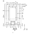
図1は、本発明の第1実施形態に係る有機EL装置の模式的な平面図である。図2(a)(b)(c)は、図1の有機EL装置の断面図であり、図2(a)は切断線IIa−IIaでの切断面、図2(b)は切断線IIb−IIbでの切断面、図2(c)は切断線IIc−IIcでの切断面をそれぞれ示す。
Hereinafter, embodiments of the present invention will be described in detail with reference to the accompanying drawings.
FIG. 1 is a schematic plan view of an organic EL device according to the first embodiment of the present invention. 2A, 2B, and 2C are cross-sectional views of the organic EL device of FIG. 1, in which FIG. 2A is a cut surface taken along a cutting line IIa-IIa, and FIG. 2B is a cutting line IIb. FIG. 2C shows a cut surface taken along the cutting line IIc-IIc.
有機EL装置1は、たとえば、照明デバイス、ディスプレイ用バックライトなどに用いられる。この有機EL装置1は、第1基板2を備えている。第1基板2は、この実施形態では平面視長方形状に形成されており、1対の短辺および1対の長辺を有している。
以下では、便宜的に、第1基板2の短辺に平行な方向(幅方向)をX方向とし、第1基板2の長辺に平行な方向(長さ方向)をY方向とし、第1基板2の厚さ方向に平行な方向をZ方向として本実施形態を説明する。また、Z方向については、第1基板2が下側に配置される有機EL装置1の基本姿勢を基準として、上下方向ということがある。
The
Hereinafter, for convenience, a direction (width direction) parallel to the short side of the
第1基板2としては、たとえば、ガラス基板、プラスチック基板、SUS基板を適用できる。第1基板2としてガラス基板やプラスチック基板などの透明基板が適用される場合、有機EL装置1は、第1基板2の側(下側)へ光を取り出すボトム・エミッション型として構成される。一方、第1基板2としてSUS基板などの不透明基板が適用される場合、有機EL装置1は、第1基板2とは反対側(上側)へ光を取り出すトップ・エミッション型として構成される。また、第1基板2の厚さは、たとえば、第1基板2がフレキシブル性を有する程度の値であり、具体的には、0.01〜1mmである。以下では、有機EL装置1がボトム・エミッション型であるとして、本実施形態を説明する。
For example, a glass substrate, a plastic substrate, or a SUS substrate can be applied as the
第1基板2上には、第1基板2の一短辺に沿ってアノード端子3およびカソード端子4が設けられている。また、第1基板2上には、Y方向において端子が配置される側(端子側)とは反対側に有機EL素子5が設けられている。
そして、有機EL装置1は、各端子3,4および有機EL素子5を封止するための導電封止層6と、導電封止層6を支持するための第2基板7とを有している。なお、図1は、第2基板7を取り外した状態の有機EL装置1を示している。
On the
The
有機EL素子5は、第1基板2の上面8(一方面)に形成された第1電極としてのアノード電極9と、アノード電極9に対向配置された第2電極としてのカソード電極10と、アノード電極9とカソード電極10との間に介在された有機化合物層11とを有している。
アノード電極9としては、たとえば、ITO(酸化インジウムと酸化錫との固溶体)、IZO(酸化インジウム亜鉛)、ZnO(酸化亜鉛)などの透明電極材料からなる電極膜を適用できる。アノード電極9の膜厚は、たとえば、0.1〜1μmである。そのような透明電極膜の抵抗は、たとえば、シート抵抗が3Ω/□程度である。また、アノード電極9は、この実施形態では平面視長方形状に形成されている。
The
As the
有機化合物層11は、アノード電極9の上面に沿ってY方向端子側に延び、アノード電極9の長さ方向一側面に回りこむ断面視L字状に形成されている。また、有機化合物層11の平面形状は、この実施形態ではアノード電極9よりも長さおよび幅のいずれも小さい長方形である。有機化合物層11の外周とアノード電極9の外周との間には、Y方向端子側が開放された平面視コ字状の第1ギャップ12が設けられている。この第1ギャップ12には、アノード電極9の周縁部13が平面視コ字状に露出している。
The
また、有機化合物層11は、たとえば、Z方向においてアノード電極9の側から順に正孔注入層、正孔輸送層、発光層、電子輸送層および電子注入層が積層された構造を有している。
正孔注入層の材料としては、たとえば、アリールアミン類、フタロシアニン類(たとえば、銅フタロシアニンなど)など、正孔注入層の材料として通常用いられるものが挙げられる。
The
Examples of the material for the hole injection layer include those usually used as the material for the hole injection layer, such as arylamines and phthalocyanines (for example, copper phthalocyanine).
正孔輸送層の材料としては、たとえば、アリールアミン類など、正孔輸送層の材料として通常用いられるものが挙げられる。
発光層は、たとえば、Alq3などの蛍光を示す金属錯体系材料に蛍光色素をドープして構成されている。たとえば、赤色発光層の材料としては、Alq3にDCMがドープされたもの、たとえば、緑色発光層の材料としては、Alq3にCoumaline(クマリン)がドープされたもの、たとえば、青色発光層の材料としては、Alq3にPerylene(ペリレン)がドープされたものなどが挙げられる。
Examples of the material for the hole transport layer include those usually used as the material for the hole transport layer, such as arylamines.
The light emitting layer is configured by, for example, doping a metal complex material showing fluorescence such as Alq 3 with a fluorescent dye. For example, as a material of the red light emitting layer, Alq 3 is doped with DCM, for example, as a material of the green light emitting layer, Alq 3 is doped with Coumarin, for example, a material of the blue light emitting layer. For example, Alq 3 doped with Perylene (perylene) may be used.
電子輸送層の材料としては、たとえば、アルミ錯体、オキサジアゾール類、トリアゾール類、フェナントロリン類など、電子輸送層の材料として通常用いられるものが挙げられる。
電子注入層の材料としては、たとえば、リチウムなどのアルカリ金属、フッ化リチウム、酸化リチウム、リチウム錯体など、電子注入層の材料として通常用いられるものが挙げられる。
Examples of the material for the electron transport layer include those usually used as the material for the electron transport layer, such as aluminum complexes, oxadiazoles, triazoles, and phenanthrolines.
Examples of the material for the electron injection layer include those commonly used as materials for the electron injection layer, such as alkali metals such as lithium, lithium fluoride, lithium oxide, and lithium complexes.
なお、正孔注入層および電子注入層は、省略されてもよい。
カソード電極10としては、たとえば、Al(アルミニウム)、Ca(カルシウム)、Mg−Al(マグネシウム−アルミニウム合金)、Al−Li(アルミニウム−リチウム)合金などの金属材料からなる電極膜を適用できる。カソード電極10の膜厚は、たとえば、0.01〜0.5μmである。そのような金属電極膜の抵抗は、一般に、前述の透明電極膜よりも低く、たとえば、シート抵抗が1Ω/□程度である。
Note that the hole injection layer and the electron injection layer may be omitted.
As the
カソード電極10は、有機化合物層11の上面に沿ってY方向端子側に延び、有機化合物層11の長さ方向一側面に回りこむ断面視L字状に形成されている。また、カソード電極10の平面形状は、この実施形態では有機化合物層11よりも幅の小さい長方形である。そして、このカソード電極10における有機化合物層11に回りこむ部分には、カソード端子4が一体的に接続されている。
The
また、カソード電極10の外周と有機化合物層11の外周との間には、Y方向端子側が開放された平面視コ字状の第2ギャップ14が設けられている。この第2ギャップ14には、有機化合物層11の周縁部15が平面視コ字状に露出している。
アノード端子3は、たとえば、カソード電極10と同一の材料からなる。このアノード端子3は、この実施形態では、アノード電極9とは分離して、平面視正方形状に形成されている。アノード端子3は、Y方向端子側が開放された平面視コ字状の周縁部13の1対の延長線上のそれぞれに配置されている。したがって、第1基板2の上面8には、1対のアノード端子3およびカソード端子4が、互いに間隔を空けてX方向に直線上に配列されている。
In addition, a
The
このような構造の有機EL素子5では、平面視においてアノード電極9、有機化合物層11およびカソード電極10が重なる一点鎖線で囲まれる領域が、電子と正孔との再結合により発光する領域(発光領域16)とされる。
第2基板7としては、たとえば、ポリイミド基板、ガラス基板、プラスチック基板などの絶縁性基板を適用できる。また、第2基板7の厚さは、たとえば、第2基板7がフレキシブル性を有する程度の値であり、具体的には、0.01〜1mmである。
In the
As the
導電封止層6は、Z方向に間隔を空けて有機EL素子5に対向配置されたキャップ部17と、キャップ部17と第1基板2との間に有機EL素子5を封じるためのシール部18とを一体的に有している。導電封止層6は、たとえば、銅(Cu)、アルミニウム(Al)などの金属材料からなる。
キャップ部17は、第2基板7の内側面19(第1基板2との対向面)のほぼ全域に薄膜状に形成されており、アノード端子3およびカソード端子4の端部を露出させるように、有機EL素子5の全域、アノード端子3およびカソード端子4に対向している。また、キャップ部17の厚さは、たとえば、0.1〜50μmである。
The
The
シール部18は、有機EL素子5の周囲を取り囲む平面視略四角環状に形成されており、第1ギャップ12から露出するコ字状の周縁部13に対して線状に接触するとともに、第1ギャップ12の延長線上に配置された1対のアノード端子3および1対のアノード端子3間に配置されたカソード端子4に接触している。シール部18の厚さは、たとえば、1〜200μmである。
The
上記のような導電封止層6には、カソード端子4の近傍に、その一部が除去された除去領域27が形成されている。これにより、導電封止層6は、アノード電極9の周縁部13およびアノード端子3に電気的に接続された第1領域としてのアノード領域20と、カソード端子4に電気的に接続された第2領域としてのカソード領域21とに絶縁分離されている。キャップ部17およびシール部18のそれぞれは、アノード領域20側の第1キャップ部22および線状接続部としての第1シール部23、カソード領域21側の第2キャップ部24および第2シール部25とに分離される。
In the
カソード領域21は、この実施形態では平面視矩形状である。このカソード領域21を取り囲む除去領域27は、平面視コ字状に形成されており、Y方向端子側に開放されている。
そして、有機EL素子5は、第1基板2および導電封止層6により形成される中空部分26に収容されており、その全周囲がシール部18で囲まれている。中空部分26は、除去領域27のみを介して外部と流通可能とされている。
In this embodiment, the
The
この中空部分26には、絶縁体が充填されることにより絶縁層28が形成されている。絶縁層28の材料としては、たとえば、エポキシ樹脂など封止用の樹脂として通常用いられるものが挙げられる。
図3(a)〜(e)は、図1および図2に示す有機EL装置の製造方法を工程順に示す図である。
An insulating
3A to 3E are views showing a method of manufacturing the organic EL device shown in FIGS. 1 and 2 in the order of steps.
上記有機EL装置1を製造するには、たとえば、図3(a)に示すように、蒸着法、スパッタ法などにより、第1基板2上に、アノード電極9、有機化合物層11、カソード電極10およびカソード端子4が、上記した形状となるように順に形成される。カソード端子4およびアノード端子3は、カソード電極10を形成する工程において、同時にパターニングすることにより形成される。
In order to manufacture the
一方、図3(b)に示すように、導電薄膜(たとえば、厚さがシール部18と同程度のもの)が形成された第2基板7が用意され、導電薄膜がパターニングされることにより、アノード領域20およびカソード領域21に分離される。導電薄膜のパターニング後、各領域の導電薄膜が所定パターンにエッチバックされることにより、シール部18(第1シール部23および第2シール部25)が形成される。
On the other hand, as shown in FIG. 3B, a
そして、図3(c)に示すように、第1基板2と第2基板7とが位置合わせされ、第1ギャップ12から露出するアノード電極9の周縁部13、アノード端子3およびカソード端子4に対して、シール部18が接合される。これにより、図3(d)に示すように、有機EL素子5が第1基板2および導電封止層6により形成される中空部分26に封止される。
Then, as shown in FIG. 3C, the
その後、図3(e)に示すように、中空部分26およびシール部18の外周に封止用の樹脂が注入される。具体的には、第1シール部23と第2シール部25との間(隙間)から中空部分26に樹脂が注入され、有機EL装置1の端面からシール部18の外周に樹脂が注入される。これにより、絶縁層28が形成される。
以上の工程を経て、図1および図2に示す有機EL装置1が得られる。
Thereafter, as shown in FIG. 3 (e), a sealing resin is injected into the outer periphery of the
Through the above steps, the
この有機EL装置1では、アノード端子3−カソード端子4間に電圧が印加されることにより、アノード電極9およびカソード電極10のそれぞれに、導電封止層6のアノード領域20およびカソード領域21のそれぞれを介して電圧が印加される。具体的には、アノード電極9には、コ字状の周縁部13に接合されたアノード領域20の第1シール部23により電圧が印加される。
In the
電圧の印加により、アノード電極9から正孔が、カソード電極10から電子が、有機化合物層11中にそれぞれ注入されることによって、電子と正孔とが有機化合物層11の発光層で再結合し、光が生成される。生成された光は、第1基板2の側へ取り出される。
この有機EL装置1によれば、アノード電極9に対して電気的なコンタクトを形成するための電極として、有機EL素子5の全域に対向するキャップ部17および有機EL素子5の周囲を取り囲むシール部18を利用することができる。そして、第1シール部23は、平面視コ字状に露出するアノード電極9の周縁部13に線状に接触している。そのため、導電封止層6を、アノード電極9に対して大きな面積で接続することができる。これにより、導電封止層6が接続されたアノード電極9において等電位部分の面積を大きくすることができ、しかも、有機EL素子5の発光領域16を、平面視コ字状の等電位面で取り囲むことができる。
By applying a voltage, holes are injected from the
According to the
その結果、電圧の印加時にアノード電極9の周縁部13全体が等電位となるため、アノード電極9の発光領域16内における電位ムラを抑制することができる。したがって、アノード電極9の厚さを大きくしなくても、有機化合物層11に対する正孔の供給ムラを低減することができる。しかも、第1シール部23が、カソード電極10の抵抗よりもシート抵抗が大きいアノード電極9に接続されているため、より効果的に、有機化合物層11に対する正孔の供給ムラを低減することができる。
As a result, since the entire
そのため、有機EL素子5のフレキシブル性などの特性の低下を抑制しつつ、有機EL素子5の面内における輝度のバラツキを抑制することができる。よって、有機EL素子5の大面積化および高輝度化を図ることができる。
また、第1シール部23がアノード電極9の周縁部13に沿って線状に接触するため、アノード電極9の周縁部13に囲まれる中央部(すなわち、発光領域16)の面積を十分確保することができる。そのため、有機EL素子5の光取出効率の低下を抑制することもできる。
Therefore, variation in luminance within the surface of the
Further, since the
また、有機EL素子5が、第1基板2および導電封止層6により形成される中空部分26に収容されており、その全周囲がシール部18で囲まれているため、酸素や水分などの中空部分26への侵入を遮断することができる。その結果、有機EL素子5の劣化を抑制することができる。換言すれば、有機EL素子5(とくに有機化合物層11)への酸素または水分の侵入を抑制する導電封止層6が、アノード電極9への給電のために兼用されている。これにより、有機EL素子5の特性劣化の抑制と、輝度ムラの低減とが同時に達成される。
In addition, since the
一方、上記のような構成の有機EL装置1において、アノード電極9の発光領域16内における電位ムラを抑制する方策として、たとえば、アノード電極9の外周に沿って補助配線を設け、当該補助配線をアノード電極9の外周縁に接触させることが考えられる。しかし、このような方策では、アノード電極9の外側に補助配線を設置するためのスペースが必要となる。そのため、有機EL素子5が複雑化・大型化するという不具合を生じる。また、補助配線の抵抗を維持したままアノード電極9の外方への補助配線のはみ出し量をできる限り低減するために、補助配線の厚さを大きくすることが考えられるかも知れない。しかし、そうすると、有機EL素子5のフレキシブル性が低下する。
On the other hand, in the
これに対し、上記の有機EL装置1によれば、有機EL素子5を封止するための導電封止層6を利用して、アノード電極9に対する電気的なコンタクトが形成される。この場合、電気的なコンタクトを形成するためのスペースは、アノード電極9の外周に補助配線を設ける場合よりも、小さくて済む。その結果、有機EL素子5の簡素化および薄型化を図ることができる。
On the other hand, according to the
また、導電封止層6のアノード領域20およびカソード領域21が、絶縁性の第2基板7に支持されているので、アノード電極9およびカソード電極10に接続される2つの導電領域を、1つの第2基板7に集約することができる。そのため、有機EL素子5の構造を簡素化することができる。さらに、アノード領域20およびカソード領域21は、図3(b)に示すように、導電薄膜が形成された第2基板7を用意し、導電薄膜をパターニングすることにより、簡単に形成することができる。
In addition, since the
さらに、この有機EL装置1では、第1基板2および第2基板7のいずれもがフレキシブル性を有するので、たとえば、フレキシブル性が要求される各種工業製品に好適に使用することができる。
図4は、本発明の第2実施形態に係る有機EL装置の模式的な平面図である。図5(a)(b)(c)は、図4の有機EL装置の断面図であり、図5(a)は切断線Va−Vaでの切断面、図5(b)は切断線Vb−Vbでの切断面、図5(c)は切断線Vc−Vcでの切断面をそれぞれ示す。図4および図5において、図1および図2に示す各部に対応する部分には、それらの各部と同一の参照符号を付している。また、以下では、同一の参照符号を付した部分についての詳細な説明を省略する。なお、図4は、導電基板を取り外した状態の有機EL装置を示している。
Furthermore, in this
FIG. 4 is a schematic plan view of an organic EL device according to the second embodiment of the present invention. 5A, 5B, and 5C are cross-sectional views of the organic EL device of FIG. 4, in which FIG. 5A is a cut surface taken along the cutting line Va-Va, and FIG. 5B is a cutting line Vb. FIG. 5C shows a cut surface taken along the cutting line Vc-Vc. 4 and FIG. 5, the same reference numerals are assigned to the portions corresponding to the respective portions shown in FIG. 1 and FIG. Further, in the following, detailed description of the parts denoted by the same reference numerals is omitted. FIG. 4 shows the organic EL device with the conductive substrate removed.
第1実施形態では、導電封止層6は、キャップ部17とシール部18とを一体的に有しているが、この第2実施形態の有機EL装置31では、導電封止層32は、第1基板2の厚さ方向に間隔を空けて有機EL素子5に対向配置された導電層としての導電基板33と、導電基板33と第1基板2との間に有機EL素子5を封じるための導電バンプ34とを別体的に有している。なお、図4は、導電基板33を取り外した状態の有機EL装置31を示している。
In the first embodiment, the
導電基板33は、たとえば、銅(Cu)、アルミニウム(Al)、スズ(Sn)などの金属材料からなる。導電基板33は、アノード端子3およびカソード端子4の端部を露出させるように、有機EL素子5の全域、アノード端子3およびカソード端子4に対向している。また、導電基板33の厚さは、たとえば、0.01〜1mmである。
導電バンプ34は、たとえば、銅(Cu)、アルミニウム(Al)、金(Au)、はんだなどの金属材料からなる。また、導電バンプ34は、有機EL素子5の周囲を取り囲む平面視略四角環状に形成されており、第1ギャップ12から露出するコ字状の周縁部13に対して線状に接触するとともに、第1ギャップ12の延長線上に配置された1対のアノード端子3に接触している。導電バンプ34は、導電基板33およびアノード電極9の周縁部13に対して共晶接合されており、これにより、アノード電極9とアノード端子3とを導電基板33を介して電気的に接続している。
The
The
一方、導電バンプ34は、カソード端子4を挟む1対のアノード端子3間が一部開放されている。これにより、導電バンプ34は、カソード端子4に対して接触しておらず、導電基板33とカソード端子4とを電気的に絶縁している。また、導電バンプ34の高さは、たとえば、1〜200μmである。
そして、有機EL素子5は、第1基板2および導電基板33により形成される中空部分35に収容されており、その全周囲が導電バンプ34で囲まれている。中空部分35は、導電バンプ34が一部開放されることにより形成された開孔部36のみを介して外部と流通可能とされている。
On the other hand, the
The
その他の構成は、前述の第1実施形態の場合と同様であり、動作もまた、同様である。
図6(a)〜(e)は、図4および図5に示す有機EL装置の製造方法を工程順に示す図である。
上記有機EL装置31を製造するには、たとえば、図6(a)に示すように、蒸着法、スパッタ法などにより、第1基板2上に、アノード電極9が、上記した形状となるように形成される。
Other configurations are the same as those of the first embodiment described above, and the operations are also the same.
6A to 6E are views showing the method of manufacturing the organic EL device shown in FIGS. 4 and 5 in the order of steps.
In order to manufacture the
次いで、図6(b)に示すように、たとえば、めっき法、転写法などにより、導電バンプ34が、上記した形状となるように形成される。
次いで、図6(c)に示すように、蒸着法、スパッタ法などにより、アノード電極9上に、有機化合物層11、カソード電極10およびカソード端子4が、上記した形状となるように順に形成される。カソード端子4およびアノード端子3は、カソード電極10を形成する工程において、カソード電極10のパターニングと同時にパターニングすることにより形成される。
Next, as shown in FIG. 6B, the
Next, as shown in FIG. 6C, the
次いで、図6(d)に示すように、第1基板2と導電基板33とが位置合わせされ、熱および圧力が加えられることにより、導電バンプ34に導電基板33が共晶接合される。これにより、有機EL素子5が第1基板2および導電基板33により形成される中空部分35に封止される。
その後、図6(e)に示すように、開孔部36(図6では図示せず)から封止用の樹脂を注入して絶縁層28が形成される。
Next, as shown in FIG. 6D, the
Thereafter, as shown in FIG. 6E, a sealing resin is injected from the opening 36 (not shown in FIG. 6) to form the insulating
以上の工程を経て、図4および図5に示す有機EL装置31が得られる。
この有機EL装置31によれば、導電封止層32が導電基板33と導電バンプ34とを有している。そして、導電封止層6をアノード電極9に電気的に接続する際には、図6(b)に示すように導電バンプ34を形成し、その後、図6(d)に示すように、第1基板2と導電基板33とを位置合わせし、熱および圧力を加えることにより、導電バンプ34に導電基板33を共晶接合すればよい。
Through the above steps, the
According to the
すなわち、アノード電極9に対する導電バンプ34の形成によって、アノード電極9に対する導電封止層32のコンタクト位置が決定する。そして、導電バンプ34は、たとえば、めっき法、転写法など、従来知られているバンプ形成技術により作製することができる。したがって、アノード電極9に対する導電封止層32の電気的なコンタクトを簡単に形成することができ、さらには、コンタクト位置を精密に制御することもできる。
That is, the contact position of the
その他、前述の第1実施形態と同様の作用効果については、記載を省略する。
図7は、第1実施形態の有機EL装置の第1変形例を示す図であって、図2(a)に対応する断面図である。
第1実施形態の第1変形例に係る有機EL装置41では、導電封止層6は、第2基板7に支持されておらず、Z方向に間隔を空けて有機EL素子5に対向配置され、有機EL素子5に対向する内側面43とは反対の外側面42が露出したキャップ部17と、キャップ部17と第1基板2との間に有機EL素子5を封じるためのシール部18とを一体的に有している。
In addition, description is abbreviate | omitted about the effect similar to the above-mentioned 1st Embodiment.
FIG. 7 is a diagram illustrating a first modification of the organic EL device according to the first embodiment, and is a cross-sectional view corresponding to FIG.
In the
また、絶縁層28の材料としては、たとえば、窒化シリコン、酸化シリコンなど絶縁膜として通常用いられるものが挙げられる。
そして、第1変形例に係る有機EL装置41を製造するには、たとえば、図3(a)に示した方法と同様の方法により、アノード電極9、有機化合物層11、カソード電極10、カソード端子4およびアノード端子3が形成され、その後、導電封止層6の形成に先立って、たとえば、蒸着法、スパッタ法などにより、絶縁層28が形成される。絶縁層28の形成後、たとえば、フォトリソグラフィ技術により、絶縁層28がシール部18の形状に対応するパターンにパターニングされる。そして、たとえば、蒸着法、スパッタ法などにより、導電封止層6の材料が堆積される。これにより、シール部18とキャップ部17とが同時に形成されて導電封止層6が形成される。
Moreover, as a material of the insulating
In order to manufacture the
第1実施形態の第1変形例に係る有機EL装置41によれば、導電封止層6が第2基板7に支持されることなく、キャップ部17の外側面42が露出しているので、有機EL素子5が発熱しても、その熱をキャップ部17の外側面42から効率よく放散することができる。その結果、有機EL装置41の放熱性を向上させることができる。
図8は、第1実施形態の有機EL装置の第2変形例を示す図であって、図2(a)に対応する断面図である。
According to the
FIG. 8 is a view showing a second modification of the organic EL device of the first embodiment, and is a cross-sectional view corresponding to FIG.
第1実施形態の第2変形例に係る有機EL装置51は、有機EL素子5を被覆する第1バリア層52をさらに含んでいる。
第1バリア層52は、たとえば、窒化シリコンなどの無機材料膜からなる。第1バリア層52は、アノード電極9の周縁部13から有機化合物層11の周縁部15を経由してカソード電極10の全表面を覆っている。これにより、アノード電極9と有機化合物層11との界面53およびカソード電極10と有機化合物層11との界面54が、第1バリア層52によりシールされることとなる。
The
The
第1バリア層52は、アノード電極9、有機化合物層11、カソード電極10、カソード端子4およびアノード端子3が図3(a)に示す方法により形成された後、たとえば、蒸着法、スパッタ法などにより無機材料を堆積させ、パターニングすることにより形成することができる。
第1実施形態の第2変形例に係る有機EL装置51によれば、アノード電極9と有機化合物層11との界面53およびカソード電極10と有機化合物層11との界面54が、第1バリア層52によりシールされるので、たとえ中空部分26内に残留水分や酸素などが存在しても、その残留水分および酸素と有機化合物層11との接触を効果的に抑制することができる。その結果、酸素や水分などによる有機EL素子5の劣化を一層抑制することができる。
The
According to the
図9は、第1実施形態の有機EL装置の第3変形例を示す図であって、図2(a)に対応する断面図である。
第1実施形態の第3変形例に係る有機EL装置61は、導電封止層6を被覆する第2バリア層62をさらに含んでいる。
第2バリア層62は、たとえば、窒化シリコンなどの無機材料膜からなる。第2バリア層62は、キャップ部17の内側面43の全域を覆い、除去領域27を隙間なく埋め尽くしている。
FIG. 9 is a view showing a third modification of the organic EL device of the first embodiment, and is a cross-sectional view corresponding to FIG.
The
The
第2バリア層62は、導電薄膜(図示せず)が図3(b)に示すようにエッチバックされてシール部18が形成された後、たとえば、蒸着法、スパッタ法などにより無機材料を導電封止層6上に堆積させ、パターニングすることにより形成することができる。
第1実施形態の第3変形例に係る有機EL装置61によれば、キャップ部17の内側面43および除去領域27が第2バリア層62によりシールされるので、特に、除去領域27から中空部分26への水分や酸素などの侵入を効果的に抑制することができる。その結果、酸素や水分などによる有機EL素子5の劣化を一層抑制することができる。
After the conductive thin film (not shown) is etched back and the
According to the
図10は、第1実施形態の有機EL装置の第4変形例を示す図であって、図2(a)に対応する断面図である。
第1実施形態の第4変形例に係る有機EL装置71は、導電封止層6を被覆する第3バリア層72をさらに含んでいる。
第3バリア層72は、たとえば、窒化シリコンなどの無機材料膜からなる。第3バリア層72は、第2基板7とキャップ部17との間の全域に介在されている。
FIG. 10 is a view showing a fourth modification of the organic EL device of the first embodiment, and is a cross-sectional view corresponding to FIG.
The
The
第3バリア層72は、たとえば、蒸着法、スパッタ法などにより、第2基板7の表面に積層し、その後、第3バリア層72上に導電薄膜(図示せず)を形成することにより、第2基板7とキャップ部17(導電薄膜)との間に介在させることができる。
第1実施形態の第4変形例に係る有機EL装置71によれば、キャップ部17および除去領域27が、第2基板7だけでなく第3バリア層72によってもシールされているので、特に、除去領域27から中空部分26への水分や酸素などの侵入を効果的に抑制することができる。その結果、酸素や水分などによる有機EL素子5の劣化を一層抑制することができる。
The
According to the
図11は、第2実施形態の有機EL装置の第1変形例を示す図であって、図5(a)に対応する断面図である。
第2実施形態の第1変形例に係る有機EL装置81では、導電バンプ34は、樹脂製コア82と、樹脂製コア82を被覆する導電被覆膜83とからなる。
樹脂製コア82の材料としては、たとえば、エポキシ樹脂、ポリウレタン樹脂などが挙げられる。また、樹脂製コア82の高さは、たとえば、1〜200μmである。
FIG. 11 is a diagram illustrating a first modification of the organic EL device according to the second embodiment, and is a cross-sectional view corresponding to FIG.
In the
Examples of the material of the
導電被覆膜83の材料としては、たとえば、金(Au)などの金属が挙げられる。また、導電被覆膜83の厚さは、たとえば、0.01〜1μmである。
このような導電バンプ34は、アノード電極9が図6(a)に示すように第1基板2上に形成された後、たとえば、樹脂ペーストが導電バンプ34のパターン状に形成され、その後、蒸着法、スパッタ法などにより金属材料が堆積され、パターニングされることによって形成することができる。
Examples of the material of the
Such a
第2実施形態の第1変形例に係る有機EL装置81によれば、導電バンプ34の全体が金属材料ではなく、そのコアが樹脂材料であるため、金属材料の使用量を低減することができる。その結果、コストを低減することができる。また、樹脂材料が、たとえば、熱硬化性樹脂であれば、有機EL素子5が発熱しても軟化し難いので、有機EL素子5の曲げ耐性を向上させることができる。
According to the
さらには、樹脂製コア82の材料としてヤング率の低い樹脂を使用することにより、有機EL素子5を曲げたときに生じる応力を、効率よく分散させることができる。
図12は、第2実施形態の有機EL装置の第2変形例を示す図であって、図5(a)に対応する断面図である。
第2実施形態の第2変形例に係る有機EL装置91は、導電バンプ34とアノード電極9との間に介在された密着層92をさらに含んでいる。
Further, by using a resin having a low Young's modulus as the material of the
FIG. 12 is a diagram illustrating a second modification of the organic EL device according to the second embodiment, and is a cross-sectional view corresponding to FIG.
The
密着層92は、たとえば、金(Au)などの金属材料からなる。密着層92は、たとえば、アノード電極9の周縁部13の表面からその外方へ延び、アノード電極9の全側面に回りこむ断面視L字状に形成されており、アノード電極9の外周端の全域を被覆している。
そして、導電バンプ34は、密着層92におけるアノード電極9の周縁部13上の部分に接合されている。
The
The
このような密着層92は、アノード電極9が図6(a)に示すように第1基板2上に形成された後、たとえば、蒸着法、スパッタ法などにより金属材料が堆積され、パターニングされることにより、形成することができる。そして、導電バンプ34は、図6(b)に示した方法と同様の方法により、密着層92上に所定の形状となるように形成すればよい。
Such an
第2実施形態の第2変形例に係る有機EL装置91によれば、導電バンプ34とアノード電極9との間に密着層92が介在されている。そのため、アノード電極9および密着層92が、接合性の良好な組み合わせ(たとえば、アノード電極9がITOであり、密着層92がAuである組み合わせ)であれば、導電バンプ34とアノード電極9との接合性を向上させることができる。そのため、導電バンプ34によるシール性を向上させることができる。
According to the
また、アノード電極9の外周端の全域が密着層92により被覆されているため、アノード電極9の側面と水分との接触を抑制することができる。したがって、水分を比較的透過させやすい材料をアノード電極9の材料として適用しても、アノード電極9と水分との接触が抑制されるので、アノード電極9に侵入する水分を低減することができる。
以上、本発明の実施形態について説明したが、本発明は他の形態で実施することもできる。
In addition, since the entire area of the outer peripheral edge of the
As mentioned above, although embodiment of this invention was described, this invention can also be implemented with another form.
たとえば、第1実施形態では、導電封止層6は、アノード電極9およびカソード電極10の両方に電気的に接続されているが、いずれか一方のみに接続されていてもよい。一方、第2実施形態では、導電封止層6,32は、アノード電極9のみに電気的に接続されているが、アノード電極9およびカソード電極10の両方に接続されていてもよい。
また、本発明は、トップ・エミッション型、ボトム・エミッション型の有機EL装置のいずれにも適用することができる。
For example, in the first embodiment, the
Further, the present invention can be applied to both a top emission type and a bottom emission type organic EL device.
たとえば、図13に示す有機EL装置101が、トップ・エミッション型である。有機EL装置101は、SUS基板などの不透明な第1基板2と、第1基板2の上面8全域に形成された絶縁層102と、絶縁層102上に順に積層された、アノード電極9、有機化合物層11およびカソード電極10とを備えている。アノード電極9の材料は特に制限されず、透明電極材料、不透明電極材料のいずれであってもよい。カソード電極10の材料は、ITOなどの透明電極材料が適用される。また、絶縁層28(エポキシ樹脂など)、導電封止層6(ITOなど)、第3バリア層72(SiNなど)および第2基板2についても、透明な材料が用いられる。したがって、有機化合物層11で生成された光は、透明なカソード電極10、絶縁層28、導電封止層32、第3バリア層72を透過し、第2基板7から取り出される。
For example, the
また、アノード電極9に対する導電封止層6,32のコンタクトは、アノード電極9の周縁部13の全周に沿って1つ形成される必要はなく、たとえば、アノード電極9の周縁部13に沿って線状に接触する線状接続部が、アノード電極9の周方向に沿って所定の間隔を空けて複数形成されていてもよい。
その他、特許請求の範囲に記載された事項の範囲で種々の設計変更を施すことが可能である。
Further, it is not necessary to form one contact of the conductive sealing layers 6 and 32 with the
In addition, various design changes can be made within the scope of the matters described in the claims.
1 有機EL装置
2 第1基板
5 有機EL素子
6 導電封止層
7 第2基板
9 アノード電極
10 カソード電極
11 有機化合物層
13 (アノード電極の)周縁部
20 アノード領域
21 カソード領域
23 第1シール部
31 有機EL装置
32 導電封止層
33 導電基板
34 導電バンプ
41 有機EL装置
51 有機EL装置
52 第1バリア層
61 有機EL装置
62 第2バリア層
71 有機EL装置
72 第3バリア層
81 有機EL装置
82 樹脂製コア
83 導電被覆膜
91 有機EL装置
DESCRIPTION OF
Claims (11)
平面視矩形状の第1電極、前記第1電極に対向配置された平面視矩形状の第2電極、および前記第1電極と前記第2電極との間に介在された有機化合物層を有し、前記第1基板上に設けられた有機EL素子と、
前記第1基板上に設けられ、前記有機EL素子を覆うことにより前記有機EL素子を封止する導電封止層と、
前記第1基板上に設けられ、前記第1電極および前記第2電極にそれぞれ接続される第1端子および第2端子とを含み、
前記第1電極は、前記第2電極の抵抗よりもシート抵抗が大きい電極膜であって、平面視で前記有機化合物層の外周の外側に露出する前記第1電極の周縁部の形状が、前記第2端子側が開放された平面視コ字状であり、
前記第2電極は、前記第1電極の前記周縁部で取り囲まれていない一辺側から外側に引き出されることで、前記第2端子が形成され、
前記導電封止層は、前記第1基板の厚さ方向に間隔を空けて前記有機EL素子に対向配置され、平面視で前記有機EL素子を覆う導電性のキャップ部と、前記導電性のキャップ部の前記第1基板側の面上に設けられ、前記第2端子に対応する部分を除いて前記有機EL素子の周囲を取り囲む平面視略四角環状に形成された導電性のシール部とから構成された第1領域を有し、
前記導電性のシール部は、前記第1電極の周縁部と平面視コ字状に線状に接触して電気的に接続されるとともに、前記第1端子と接触して電気的に接続され、
前記第1基板および前記導電封止層により形成され、前記有機EL素子を収容する中空部分には、絶縁体が充填されることにより絶縁層が形成されている、有機EL装置。 A first substrate;
A first electrode having a rectangular shape in plan view , a second electrode having a rectangular shape in plan view arranged opposite to the first electrode, and an organic compound layer interposed between the first electrode and the second electrode An organic EL device provided on the first substrate;
A conductive sealing layer provided on the first substrate and sealing the organic EL element by covering the organic EL element ;
A first terminal and a second terminal provided on the first substrate and connected to the first electrode and the second electrode, respectively ;
The first electrode is an electrode film having a sheet resistance larger than the resistance of the second electrode, and the shape of the peripheral portion of the first electrode exposed outside the outer periphery of the organic compound layer in a plan view is The second terminal side is an open U shape in plan view ,
The second electrode is pulled out from one side not surrounded by the peripheral edge of the first electrode , whereby the second terminal is formed ,
The conductive sealing layer is disposed to face the organic EL element with a space in the thickness direction of the first substrate, and covers the organic EL element in plan view, and the conductive cap A conductive seal portion provided on the surface of the first substrate side of the portion and formed in a substantially square annular shape in plan view surrounding the periphery of the organic EL element except for a portion corresponding to the second terminal A first region formed,
The conductive seal portion is electrically connected in contact with the peripheral edge portion of the first electrode in a line shape in a U shape in plan view, and is electrically connected in contact with the first terminal.
An organic EL device, wherein an insulating layer is formed by filling an insulating material in a hollow portion that is formed by the first substrate and the conductive sealing layer and that accommodates the organic EL element .
前記第2電極が、金属材料からなる電極膜からなる、請求項1〜8のいずれか一項に記載の有機EL装置。 The first electrode is made of an electrode film made of a transparent electrode material,
Wherein the second electrode consists of an electrode film made of a metal material, an organic EL device according to any one of claims 1-8.
前記第1電極が、前記第1基板の上面に形成されている、請求項9に記載の有機EL装置。 The first substrate comprises a transparent substrate;
The organic EL device according to claim 9 , wherein the first electrode is formed on an upper surface of the first substrate.
前記第2電極が、カソード電極である、請求項1〜10のいずれか一項に記載の有機EL装置。 The first electrode is an anode electrode;
The second electrode is a cathode electrode, the organic EL device according to any one of claims 1-10.
Priority Applications (1)
| Application Number | Priority Date | Filing Date | Title |
|---|---|---|---|
| JP2009174301A JP5748397B2 (en) | 2009-07-27 | 2009-07-27 | Organic EL device |
Applications Claiming Priority (1)
| Application Number | Priority Date | Filing Date | Title |
|---|---|---|---|
| JP2009174301A JP5748397B2 (en) | 2009-07-27 | 2009-07-27 | Organic EL device |
Publications (2)
| Publication Number | Publication Date |
|---|---|
| JP2011029022A JP2011029022A (en) | 2011-02-10 |
| JP5748397B2 true JP5748397B2 (en) | 2015-07-15 |
Family
ID=43637541
Family Applications (1)
| Application Number | Title | Priority Date | Filing Date |
|---|---|---|---|
| JP2009174301A Expired - Fee Related JP5748397B2 (en) | 2009-07-27 | 2009-07-27 | Organic EL device |
Country Status (1)
| Country | Link |
|---|---|
| JP (1) | JP5748397B2 (en) |
Families Citing this family (7)
| Publication number | Priority date | Publication date | Assignee | Title |
|---|---|---|---|---|
| JP5010698B2 (en) | 2010-03-02 | 2012-08-29 | 株式会社東芝 | LIGHTING DEVICE AND MANUFACTURING METHOD THEREOF |
| JP2013531345A (en) * | 2010-07-08 | 2013-08-01 | エルジー・ケム・リミテッド | ORGANIC LIGHT EMITTING ELEMENT AND MANUFACTURING METHOD THEREOF |
| JP2012174558A (en) * | 2011-02-22 | 2012-09-10 | Panasonic Corp | Organic el device |
| JP2013196919A (en) * | 2012-03-21 | 2013-09-30 | Sony Corp | Organic el display device, organic el display device manufacturing method, and color filter substrate |
| KR20140146953A (en) | 2013-06-18 | 2014-12-29 | 삼성디스플레이 주식회사 | Organic light emitting display apparatus |
| JP6341999B2 (en) * | 2013-09-30 | 2018-06-13 | エルジー ディスプレイ カンパニー リミテッド | ORGANIC LIGHT-EMITTING ELEMENT AND MANUFACTURING METHOD |
| US11522156B2 (en) * | 2018-03-29 | 2022-12-06 | Sharp Kabushiki Kaisha | Display device with light-transmissive conductive film between sealing films |
Family Cites Families (3)
| Publication number | Priority date | Publication date | Assignee | Title |
|---|---|---|---|---|
| JP4151634B2 (en) * | 2004-09-24 | 2008-09-17 | セイコーエプソン株式会社 | SEMICONDUCTOR DEVICE AND ITS MANUFACTURING METHOD, CIRCUIT BOARD, ELECTRO-OPTICAL DEVICE, AND ELECTRONIC DEVICE |
| WO2008062645A1 (en) * | 2006-11-21 | 2008-05-29 | Konica Minolta Holdings, Inc. | Organic electroluminescent panel and sealing member |
| JP2008288012A (en) * | 2007-05-17 | 2008-11-27 | Seiko Epson Corp | Electroluminescence device and its manufacturing method |
-
2009
- 2009-07-27 JP JP2009174301A patent/JP5748397B2/en not_active Expired - Fee Related
Also Published As
| Publication number | Publication date |
|---|---|
| JP2011029022A (en) | 2011-02-10 |
Similar Documents
| Publication | Publication Date | Title |
|---|---|---|
| JP5748397B2 (en) | Organic EL device | |
| US9997589B2 (en) | Display device | |
| JP5208521B2 (en) | OLED device | |
| EP2983223B1 (en) | Organic light-emitting device and method for manufacturing same | |
| CN107895728B (en) | Array substrate, manufacturing method thereof and display device comprising array substrate | |
| US8829501B2 (en) | Large area light emitting device comprising organic light emitting diodes | |
| KR101798212B1 (en) | Organic electroluminescent device | |
| KR20120123490A (en) | Optoelectronic device array | |
| WO2019097823A1 (en) | Display device | |
| US9502684B2 (en) | Organic electroluminescence device and method for manufacturing the same | |
| KR20120115838A (en) | Organic light emitting diode display | |
| KR20170042611A (en) | Optoelectronic component and method for producing same | |
| KR100736576B1 (en) | Light emitting diode and method for manufacturing the same | |
| JP4823685B2 (en) | EL device and manufacturing method thereof | |
| JP2000357585A (en) | Organic el element | |
| KR20150143405A (en) | Electrical connection of an oled device | |
| WO2012102268A1 (en) | Organic electroluminescent element and illumination device | |
| JP2008293787A (en) | El element | |
| JP2001223079A (en) | Organic el display element | |
| WO2013128621A1 (en) | Organic el device and manufacturing method therefor | |
| JP7353331B2 (en) | light emitting device | |
| JP6329177B2 (en) | Light emitting device | |
| WO2013145226A1 (en) | El device and method of manufacturing same | |
| US20170012239A1 (en) | Light emitting apparatus | |
| JP2003007474A (en) | Organic electric field light emitting device |
Legal Events
| Date | Code | Title | Description |
|---|---|---|---|
| A621 | Written request for application examination |
Free format text: JAPANESE INTERMEDIATE CODE: A621 Effective date: 20120712 |
|
| A977 | Report on retrieval |
Free format text: JAPANESE INTERMEDIATE CODE: A971007 Effective date: 20121129 |
|
| A131 | Notification of reasons for refusal |
Free format text: JAPANESE INTERMEDIATE CODE: A131 Effective date: 20130110 |
|
| A521 | Request for written amendment filed |
Free format text: JAPANESE INTERMEDIATE CODE: A523 Effective date: 20130308 |
|
| A02 | Decision of refusal |
Free format text: JAPANESE INTERMEDIATE CODE: A02 Effective date: 20131010 |
|
| A521 | Request for written amendment filed |
Free format text: JAPANESE INTERMEDIATE CODE: A523 Effective date: 20140110 |
|
| A911 | Transfer to examiner for re-examination before appeal (zenchi) |
Free format text: JAPANESE INTERMEDIATE CODE: A911 Effective date: 20140121 |
|
| A912 | Re-examination (zenchi) completed and case transferred to appeal board |
Free format text: JAPANESE INTERMEDIATE CODE: A912 Effective date: 20140214 |
|
| A521 | Request for written amendment filed |
Free format text: JAPANESE INTERMEDIATE CODE: A523 Effective date: 20150403 |
|
| A61 | First payment of annual fees (during grant procedure) |
Free format text: JAPANESE INTERMEDIATE CODE: A61 Effective date: 20150512 |
|
| R150 | Certificate of patent or registration of utility model |
Ref document number: 5748397 Country of ref document: JP Free format text: JAPANESE INTERMEDIATE CODE: R150 |
|
| R250 | Receipt of annual fees |
Free format text: JAPANESE INTERMEDIATE CODE: R250 |
|
| LAPS | Cancellation because of no payment of annual fees |