JP5723779B2 - Large area patterning of nano size shape - Google Patents
Large area patterning of nano size shape Download PDFInfo
- Publication number
- JP5723779B2 JP5723779B2 JP2011536331A JP2011536331A JP5723779B2 JP 5723779 B2 JP5723779 B2 JP 5723779B2 JP 2011536331 A JP2011536331 A JP 2011536331A JP 2011536331 A JP2011536331 A JP 2011536331A JP 5723779 B2 JP5723779 B2 JP 5723779B2
- Authority
- JP
- Japan
- Prior art keywords
- layer
- pattern
- resist layer
- substrate
- resist
- Prior art date
- Legal status (The legal status is an assumption and is not a legal conclusion. Google has not performed a legal analysis and makes no representation as to the accuracy of the status listed.)
- Active
Links
- 238000000059 patterning Methods 0.000 title description 14
- 239000000463 material Substances 0.000 claims description 87
- 239000000758 substrate Substances 0.000 claims description 84
- 238000000034 method Methods 0.000 claims description 61
- 238000001459 lithography Methods 0.000 claims description 19
- 238000005530 etching Methods 0.000 claims description 15
- 229910052751 metal Inorganic materials 0.000 claims description 9
- 239000002184 metal Substances 0.000 claims description 9
- 238000000151 deposition Methods 0.000 claims description 7
- 239000000853 adhesive Substances 0.000 claims description 3
- 230000001070 adhesive effect Effects 0.000 claims description 3
- 239000011368 organic material Substances 0.000 claims description 3
- 229920005573 silicon-containing polymer Polymers 0.000 claims description 3
- 239000010432 diamond Substances 0.000 claims description 2
- 229910003460 diamond Inorganic materials 0.000 claims description 2
- 229920002120 photoresistant polymer Polymers 0.000 claims description 2
- 239000002195 soluble material Substances 0.000 claims description 2
- 238000001127 nanoimprint lithography Methods 0.000 claims 3
- 238000001312 dry etching Methods 0.000 claims 1
- 239000010410 layer Substances 0.000 description 67
- 230000008569 process Effects 0.000 description 20
- 238000012545 processing Methods 0.000 description 14
- 239000002086 nanomaterial Substances 0.000 description 12
- 239000010408 film Substances 0.000 description 9
- 239000012530 fluid Substances 0.000 description 9
- 230000015572 biosynthetic process Effects 0.000 description 8
- 239000012790 adhesive layer Substances 0.000 description 5
- 239000000178 monomer Substances 0.000 description 5
- 238000010894 electron beam technology Methods 0.000 description 4
- 239000007788 liquid Substances 0.000 description 4
- 238000004519 manufacturing process Methods 0.000 description 4
- 238000003892 spreading Methods 0.000 description 4
- 230000007480 spreading Effects 0.000 description 4
- WGTYBPLFGIVFAS-UHFFFAOYSA-M tetramethylammonium hydroxide Chemical compound [OH-].C[N+](C)(C)C WGTYBPLFGIVFAS-UHFFFAOYSA-M 0.000 description 4
- VYZAMTAEIAYCRO-UHFFFAOYSA-N Chromium Chemical compound [Cr] VYZAMTAEIAYCRO-UHFFFAOYSA-N 0.000 description 3
- 229910052804 chromium Inorganic materials 0.000 description 3
- 239000011651 chromium Substances 0.000 description 3
- 230000033001 locomotion Effects 0.000 description 3
- 238000000206 photolithography Methods 0.000 description 3
- 229920000642 polymer Polymers 0.000 description 3
- VYPSYNLAJGMNEJ-UHFFFAOYSA-N Silicium dioxide Chemical compound O=[Si]=O VYPSYNLAJGMNEJ-UHFFFAOYSA-N 0.000 description 2
- XUIMIQQOPSSXEZ-UHFFFAOYSA-N Silicon Chemical compound [Si] XUIMIQQOPSSXEZ-UHFFFAOYSA-N 0.000 description 2
- 238000005229 chemical vapour deposition Methods 0.000 description 2
- 238000004140 cleaning Methods 0.000 description 2
- 239000011248 coating agent Substances 0.000 description 2
- 238000000576 coating method Methods 0.000 description 2
- 238000004891 communication Methods 0.000 description 2
- 238000010586 diagram Methods 0.000 description 2
- 238000000609 electron-beam lithography Methods 0.000 description 2
- 238000005240 physical vapour deposition Methods 0.000 description 2
- 229910052710 silicon Inorganic materials 0.000 description 2
- 239000010703 silicon Substances 0.000 description 2
- 238000004528 spin coating Methods 0.000 description 2
- 238000012546 transfer Methods 0.000 description 2
- 238000009736 wetting Methods 0.000 description 2
- 238000001015 X-ray lithography Methods 0.000 description 1
- 230000009471 action Effects 0.000 description 1
- 238000004380 ashing Methods 0.000 description 1
- QVGXLLKOCUKJST-UHFFFAOYSA-N atomic oxygen Chemical compound [O] QVGXLLKOCUKJST-UHFFFAOYSA-N 0.000 description 1
- 230000008901 benefit Effects 0.000 description 1
- 239000005388 borosilicate glass Substances 0.000 description 1
- -1 but not limited to Substances 0.000 description 1
- 238000002508 contact lithography Methods 0.000 description 1
- 230000008021 deposition Effects 0.000 description 1
- 238000011161 development Methods 0.000 description 1
- 238000003618 dip coating Methods 0.000 description 1
- KPUWHANPEXNPJT-UHFFFAOYSA-N disiloxane Chemical class [SiH3]O[SiH3] KPUWHANPEXNPJT-UHFFFAOYSA-N 0.000 description 1
- 238000000203 droplet dispensing Methods 0.000 description 1
- 230000000694 effects Effects 0.000 description 1
- 238000005516 engineering process Methods 0.000 description 1
- 239000012467 final product Substances 0.000 description 1
- 229920002313 fluoropolymer Polymers 0.000 description 1
- 239000005350 fused silica glass Substances 0.000 description 1
- 229910052736 halogen Inorganic materials 0.000 description 1
- 125000005843 halogen group Chemical group 0.000 description 1
- 239000012212 insulator Substances 0.000 description 1
- 238000002164 ion-beam lithography Methods 0.000 description 1
- 239000000203 mixture Substances 0.000 description 1
- 238000012986 modification Methods 0.000 description 1
- 230000004048 modification Effects 0.000 description 1
- 230000003287 optical effect Effects 0.000 description 1
- 229920000620 organic polymer Polymers 0.000 description 1
- 229910052760 oxygen Inorganic materials 0.000 description 1
- 239000001301 oxygen Substances 0.000 description 1
- 238000012805 post-processing Methods 0.000 description 1
- 238000004886 process control Methods 0.000 description 1
- 239000010453 quartz Substances 0.000 description 1
- 230000010076 replication Effects 0.000 description 1
- 230000003362 replicative effect Effects 0.000 description 1
- 229910052594 sapphire Inorganic materials 0.000 description 1
- 239000010980 sapphire Substances 0.000 description 1
- 239000004065 semiconductor Substances 0.000 description 1
- 239000002904 solvent Substances 0.000 description 1
- 238000003860 storage Methods 0.000 description 1
- 239000000126 substance Substances 0.000 description 1
- 239000004094 surface-active agent Substances 0.000 description 1
- 239000010409 thin film Substances 0.000 description 1
- 238000000427 thin-film deposition Methods 0.000 description 1
- 238000013518 transcription Methods 0.000 description 1
- 230000035897 transcription Effects 0.000 description 1
- 238000001039 wet etching Methods 0.000 description 1
Images


Classifications
-
- G—PHYSICS
- G03—PHOTOGRAPHY; CINEMATOGRAPHY; ANALOGOUS TECHNIQUES USING WAVES OTHER THAN OPTICAL WAVES; ELECTROGRAPHY; HOLOGRAPHY
- G03F—PHOTOMECHANICAL PRODUCTION OF TEXTURED OR PATTERNED SURFACES, e.g. FOR PRINTING, FOR PROCESSING OF SEMICONDUCTOR DEVICES; MATERIALS THEREFOR; ORIGINALS THEREFOR; APPARATUS SPECIALLY ADAPTED THEREFOR
- G03F7/00—Photomechanical, e.g. photolithographic, production of textured or patterned surfaces, e.g. printing surfaces; Materials therefor, e.g. comprising photoresists; Apparatus specially adapted therefor
- G03F7/0035—Multiple processes, e.g. applying a further resist layer on an already in a previously step, processed pattern or textured surface
-
- B—PERFORMING OPERATIONS; TRANSPORTING
- B82—NANOTECHNOLOGY
- B82Y—SPECIFIC USES OR APPLICATIONS OF NANOSTRUCTURES; MEASUREMENT OR ANALYSIS OF NANOSTRUCTURES; MANUFACTURE OR TREATMENT OF NANOSTRUCTURES
- B82Y10/00—Nanotechnology for information processing, storage or transmission, e.g. quantum computing or single electron logic
-
- B—PERFORMING OPERATIONS; TRANSPORTING
- B82—NANOTECHNOLOGY
- B82Y—SPECIFIC USES OR APPLICATIONS OF NANOSTRUCTURES; MEASUREMENT OR ANALYSIS OF NANOSTRUCTURES; MANUFACTURE OR TREATMENT OF NANOSTRUCTURES
- B82Y40/00—Manufacture or treatment of nanostructures
-
- G—PHYSICS
- G03—PHOTOGRAPHY; CINEMATOGRAPHY; ANALOGOUS TECHNIQUES USING WAVES OTHER THAN OPTICAL WAVES; ELECTROGRAPHY; HOLOGRAPHY
- G03F—PHOTOMECHANICAL PRODUCTION OF TEXTURED OR PATTERNED SURFACES, e.g. FOR PRINTING, FOR PROCESSING OF SEMICONDUCTOR DEVICES; MATERIALS THEREFOR; ORIGINALS THEREFOR; APPARATUS SPECIALLY ADAPTED THEREFOR
- G03F7/00—Photomechanical, e.g. photolithographic, production of textured or patterned surfaces, e.g. printing surfaces; Materials therefor, e.g. comprising photoresists; Apparatus specially adapted therefor
- G03F7/0002—Lithographic processes using patterning methods other than those involving the exposure to radiation, e.g. by stamping
Landscapes
- Engineering & Computer Science (AREA)
- Nanotechnology (AREA)
- Chemical & Material Sciences (AREA)
- Physics & Mathematics (AREA)
- General Physics & Mathematics (AREA)
- Crystallography & Structural Chemistry (AREA)
- Theoretical Computer Science (AREA)
- Condensed Matter Physics & Semiconductors (AREA)
- Mathematical Physics (AREA)
- Manufacturing & Machinery (AREA)
- Shaping Of Tube Ends By Bending Or Straightening (AREA)
- Exposure Of Semiconductors, Excluding Electron Or Ion Beam Exposure (AREA)
- Moulds For Moulding Plastics Or The Like (AREA)
Description
関連出願の相互参照
本出願は、米国特許法第35条第119項(e)(1)の下で、2008年11月13日に出願された米国仮特許出願第61/114,239号と2009年11月12日に出願された米国特許出願第12/616,896号の利益を主張し、これらの出願は、全体が本明細書に援用される。
This application is related to US Provisional Patent Application No. 61 / 114,239 filed on November 13, 2008 under 35 USC 35 119 (e) (1). Claiming the benefit of US patent application Ser. No. 12 / 616,896, filed Nov. 12, 2009, which applications are incorporated herein in their entirety.
ナノ加工は、例えば約100ナノメートル以下のフィーチャを有するきわめて小さい構造物の製造を含む。ナノ加工がかなり大きい効果を有する1つの用途は、集積回路の処理である。半導体処理産業は、基板上に形成される単位面積当たりの回路を増大させながら高い生産歩留まりを目指す努力をし続けているので、ナノ加工はますます重要になってきている。ナノ加工は、形成される構造物の最小フィーチャ寸法を縮小し続けながらより優れたプロセス制御を提供する。ナノ加工がこれまで利用されてきた他の開発分野には、バイオテクノロジー、光学技術、エネルギーシステムなどがある。 Nanofabrication involves the production of very small structures, for example having features of about 100 nanometers or less. One application where nanofabrication has a significant effect is in the processing of integrated circuits. As the semiconductor processing industry continues to strive for high production yields while increasing the circuits per unit area formed on the substrate, nanofabrication is becoming increasingly important. Nanofabrication provides better process control while continuing to reduce the minimum feature size of the structure being formed. Other development areas where nanofabrication has been used to date include biotechnology, optical technology, and energy systems.
例示的なナノ加工技術は、インプリント・リソグラフィと呼ばれる。例示的なインプリント・リソグラフィ・プロセスは、米国特許出願公開第2004/0065976号; 米国特許出願公開第2004/0065252号; 米国特許第6,936,194号などの多くの公報に詳細に述べられており、これらの文献はすべて、本発明の譲渡人に譲渡されている。 An exemplary nanofabrication technique is called imprint lithography. Exemplary imprint lithography processes are described in detail in many publications such as US Patent Application Publication No. 2004/0065976; US Patent Application Publication No. 2004/0065252; US Patent No. 6,936,194. All of these documents are assigned to the assignee of the present invention.
前述の米国特許出願および米国特許のそれぞれに開示されたインプリント・リソグラフィ技術は、成形可能な液体(重合性層)におけるレリーフ・パターンの形成と、そのレリーフ・パターンに対応するパターンを下の基板に転写することを含む。基板は、パターニングを容易にする所望の位置を得るために移動ステージ上に配置されてもよい。この目的のため、テンプレートは、テンプレートと基板の間に成形可能液体がある状態で基板から離間されて使用される。液体は、成形可能液体と接触するテンプレートの表面の形状に合致するパターンを記録する凝固層に凝固される。次に、テンプレートは、凝固層から分離されて、テンプレートと基板が離間される。次に、基板と凝固層は、凝固層のパターンに対応するレリーフ像を基板に転写する処理にかけられる。 The imprint lithography technique disclosed in each of the aforementioned U.S. patent applications and U.S. patents is directed to the formation of a relief pattern in a moldable liquid (polymerizable layer) and a pattern corresponding to the relief pattern on the underlying substrate. Including transcription. The substrate may be placed on a moving stage to obtain a desired position that facilitates patterning. For this purpose, the template is used spaced apart from the substrate with a moldable liquid between the template and the substrate. The liquid is solidified into a solidified layer that records a pattern that matches the shape of the template surface in contact with the moldable liquid. Next, the template is separated from the solidified layer, and the template and the substrate are separated. Next, the substrate and the solidified layer are subjected to a process of transferring a relief image corresponding to the pattern of the solidified layer to the substrate.
多くのナノパターニング応用例は、所望の結果を達成するサイズと均一形状のナノスケール・フィーチャを利用する。ナノパターンの作成に使用される多くの処理は、特定のタイプとサイズのナノパターンを成長させるために「成長」処理を使用する。残念ながら、これらのタイプの処理は、時間がかかり、所望の実施コストを効果的にもたらすために十分に制御されないサイズと形状を有するナノパターンを生成しやすい。 Many nanopatterning applications utilize nanoscale features that are sized and uniformly shaped to achieve the desired result. Many processes used to create nanopatterns use a “growth” process to grow specific types and sizes of nanopatterns. Unfortunately, these types of processing are time consuming and tend to produce nanopatterns with sizes and shapes that are not well controlled to effectively bring the desired implementation cost.
図1を参照すると、基板12上にレリーフ・パターンを形成するシステム10が示される。基板12は、基板チャック14に結合されてもよい。示された基板チャック14は、真空チャックであるが、基板チャック14は、参照により本明細書に組み込まれた「High-Precision Orientation Alignment and Gap Control Stages for Imprint Lithography Processes」と題する米国特許第6,873,087号に記載されたような真空式、ピン型、溝型または電磁式を含むがこれらに限定されない任意のチャックでよい。基板12と基板チャック14は、ステージ16上に支持されてもよい。さらに、ステージ16、基板12および基板チャック14は、台(図示せず)上に位置決めされてもよい。ステージ16は、x、yおよびz軸に沿った運動を提供してもよい。
Referring to FIG. 1, a
基板12からは、主パターニング装置17が離間されている。主パターニング装置17は、パターン面22を上に有する基板12の方に突出するメサ(段丘部)20を有するテンプレート28を有する。さらに、メサ20は、モールド20と呼ばれることがある。メサ20は、ナノインプリント・モールド20と呼ばれることもある。さらに他の実施形態では、テンプレート28に実質的にモールド20がなくてもよい。さらに他の実施形態では、モールド20は、テンプレート28と一体形成されてもよい。テンプレート28および/またはモールド20は、融解石英、石英、シリコン、有機重合体(ポリマー)、シロキサン重合体、ホウケイ酸ガラス、フルオロカーボン重合体、金属および硬化サファイアを含むがこれらに限定されない材料から形成されてもよい。図示されたように、パターニング面22は、複数の離間した凹部24と突出部26によって画定されたフィーチャを含む。しかしながら、その他の実施形態では、パターニング面22は、実質的に平滑および/または平面でもよい。パターニング面22は、基板12上に形成されたパターンの基礎を形成する元パターンを画定してもよい。主パターニング装置17は、電子ビーム(Eビーム)リソグラフィを使用して形成されてもよい。
A
主パターニング装置17は、チャック28に結合されてもよく、チャック28には、「High-Precision Orientation Alignment and Gap Control Stages for Imprint Lithography Processes」と題する米国特許第6,873,087号に記載されたような、真空式、ピン型、溝型または電磁式を含むがこれらに限定されない任意のチェックがある。さらに、チャック28は、主パターニング装置17の動きを推進するためにインプリント・ヘッド30に結合されてもよい。
The
システム10は、さらに、流体分注(ディスペンス)システム32を含む。流体分注システム32は、基板上に重合性材料34を付着させるために基板12と流体連通してもよい。システム10は、任意数の流体ディスペンサを含んでもよく、流体分注システム32は、複数の分注ユニットを含んでもよい。重合性材料34は、任意の既知の技術、例えば、液滴分注、回転塗布、浸せき塗布、化学蒸着(CVD)、物理蒸着(PVD)、薄膜蒸着、厚膜蒸着などを使用して基板12上に位置決めされてもよい。一般に、重合性材料34は、モールド20と基板12の間に所望の容積が画定される前に基板12上に配置される。しかしながら、重合性材料34は、所望の体積が得られた後で容積に充填されてもよい。
The
重合性材料34は、溶媒を主成分とする単量体またはスピンオン材料を含んでもよい。さらに、重合性材料34は、「Method to Reduce Adhesion Between a Conformable Region and a Pattern of a Mold」と題する米国特許第7,157,036号と、「Materials for Imprint Lithography」と題する米国特許出願公開第2005/0187339号に記載されたような単量体混合物を含んでもよく、これらの文献は、参照により本明細書に組み込まれる。
The
システム10は、さらに、経路42に沿ってエネルギー40を導くように結合されたエネルギー40の供給源38を含む。インプリント・ヘッド30とステージ16は、主パターニング装置17と基板12をそれぞれ重ね合わせて経路42内に配置するように構成される。システム10は、記憶装置56に記憶されたコンピュータ可読プログラムで動作するステージ16、インプリント・ヘッド30、流体分注システム32、および供給源38とデータ通信するプロセッサ54によって調整されてもよい。
The
前述のシステムおよび方法は、さらに、米国特許第6,932,934号、米国特許第7,077,992号、米国特許第6,900,881号、米国特許出願公開第2004/0124566号、米国特許出願公開第2004/0188381号および米国特許出願公開第2004/0211754号に引用されたインプリント・リソグラフィ方法およびシステムに使用されてもよく、これらの全ての文献は、参照により本明細書に組み込まれる。さらに他の実施形態では、前述のレリーフ・パターンは、任意の既知の技術、例えば、フォトリソグラフィ(G線、I線、248nm、193nm、157nm、および13.2〜13.4nmを含む様々な波長)、コンタクト・リソグラフィ、電子ビームリソグラフィ、X線リソグラフィ、イオンビーム・リソグラフィ、原子線リソグラフィによって作成されてもよい。例えば、前述のレリーフ・パターンは、参照により本明細書に組み込まれた米国特許第5,772,905号に記載された技術を使用して作成されてもよい。 The systems and methods described above are further described in US Pat. No. 6,932,934, US Pat. No. 7,077,992, US Pat. No. 6,900,881, US Patent Application Publication No. 2004/0124566, US May be used in the imprint lithography methods and systems cited in US Patent Application Publication No. 2004/0188381 and US Patent Application Publication No. 2004/0211754, all of which are incorporated herein by reference. It is. In still other embodiments, the relief pattern described above may be applied to any known technique, for example, photolithography (G-line, I-line, 248 nm, 193 nm, 157 nm, and various wavelengths including 13.2 to 13.4 nm). ), Contact lithography, electron beam lithography, X-ray lithography, ion beam lithography, atomic beam lithography. For example, the relief pattern described above may be created using the techniques described in US Pat. No. 5,772,905, which is incorporated herein by reference.
異なる幾何学的断面を有するナノ構造物は、本明細書で述べる技術を使用して作成されてもよい。一般に、この方法は、2つのフェーズを含むことがある。フェーズ1では、多数のリソグラフィ・ステップの組み合わせを使用して、成形断面を有するインプリント・テンプレート(ナノ成形テンプレートと呼ばれる)を作成してもよい。多数のリソグラフィ・ステップは、電子ビーム、インプリント・リソグラフィ、フォトリソグラフィなどの1または複数種類のリソグラフィ方法を使用してもよい。フェーズ2では、ナノ成形テンプレートをインプリント・リソグラフィ・プロセスと一緒に使用して、ナノ形状を複製する高速手法を実現してもよい。 Nanostructures having different geometric cross-sections may be created using the techniques described herein. In general, this method may include two phases. In phase 1, a combination of multiple lithography steps may be used to create an imprint template with a shaped cross section (referred to as a nanomolded template). The number of lithography steps may use one or more types of lithography methods such as electron beam, imprint lithography, photolithography. In phase 2, the nanomold template may be used in conjunction with an imprint lithography process to provide a fast technique for replicating nanoshapes.
フェーズ1: ナノ成形テンプレートの形成
一般に、フェーズ1は、多数のプロセス・ステップを含んでもよい。説明を単純にするために、本明細書ではインプリント・リソグラフィを使用するナノ成形テンプレートの形成について述べる。しかしながら、パターニング・ステップは、フォトリソグラフィ、電子ビーム・リソグラフィなどを使用してもよいことに注意されたい。
Phase 1 : Formation of nano-molded template In general, Phase 1 may include a number of process steps. For simplicity of explanation, this document describes the formation of nanomolded templates using imprint lithography. However, it should be noted that the patterning step may use photolithography, electron beam lithography, and the like.
一般に、重合体、絶縁体、金属などを含む第1の材料(例えば、非湿潤可剥性材料)の薄層が、ナノ構造材料で作成された所望の基板上に付着されてもよい。第1の材料上に第2のレジスト層(例えば、湿潤可剥性材料)が付着されてもよい。第2のレジストは、第1の材料が実質的に完全な状態のままで選択的に湿潤剥離(wet-strip)されもよい。第2のレジスト材料上に成形可能なインプリント・リソグラフィ材料が付着されてもよく、リソグラフィ材料がインプリントされてレリーフ・パターンが形成されてもよい。インプリント処理を使用してレリーフ・パターンを作成するために使用されるモールドは、電子ビーム処理により形成可能な単純な幾何学形状(例えば、線、点、穴など)で構成されてもよい。成形可能材料を下の基板に接着し易くするために、第2のレジスト材料と第3の成形可能材料の間に任意選択の接着材が付着されてもよい。接着層は、参照により本明細書に組み込まれる米国特許出願公開第2007/0212494号に更に詳しく記載されているような接着材から形成されてもよい。成形可能層のレリーフ・パターンは、必要に応じてエッチングされて成形可能材料の隆起パターンを作成してもよく、隆起パターンは、エッチング前のサイズより小さいサイズを有する。 In general, a thin layer of a first material (eg, a non-wetting peelable material) comprising a polymer, insulator, metal, etc. may be deposited on a desired substrate made of nanostructured material. A second resist layer (eg, a wet strippable material) may be deposited on the first material. The second resist may be selectively wet-striped while the first material remains substantially intact. A moldable imprint lithographic material may be deposited on the second resist material, and the lithographic material may be imprinted to form a relief pattern. A mold used to create a relief pattern using an imprint process may be composed of simple geometric shapes (eg, lines, dots, holes, etc.) that can be formed by electron beam processing. An optional adhesive may be applied between the second resist material and the third moldable material to facilitate bonding of the moldable material to the underlying substrate. The adhesive layer may be formed from an adhesive as described in more detail in US Patent Application Publication No. 2007/0212494, which is incorporated herein by reference. The relief pattern of the moldable layer may be etched as necessary to create a raised pattern of moldable material, the raised pattern having a size that is smaller than the size before etching.
エッチングされた成形可能層の上にオーバーコート材料が付着されてもよい。オーバーコート材料は、細い隆起線の上面を露出するようにエッチングされたブランケットでよい。露出された成形可能材料は、非湿潤可剥性の第1のレジスト材料まで下方に延在するトレンチを形成するようにエッチングされてもよい。非湿潤可剥性レジストは、基板に達したときに停止するようにドライエッチングされてもよい。成形可能層材料と湿潤可剥性材料は、トレンチが基板まで下方に延在する状態で非湿潤可剥性材料が残るように剥がされてもよい。基板は、表面のパターンが最終的なものである場合に所望の深さまでエッチングされてもよい。最後に、インプリント・モールドは、形状および/または向きが修正されてもよく、表面のパターンが最終的なものでない場合はプロセスがステップ2から繰り返される。 An overcoat material may be deposited over the etched moldable layer. The overcoat material may be a blanket etched to expose the top surface of the thin ridges. The exposed moldable material may be etched to form a trench extending down to the non-wet strippable first resist material. The non-wet strippable resist may be dry etched to stop when it reaches the substrate. The moldable layer material and the wet strippable material may be stripped so that the non-wet strippable material remains with the trench extending down to the substrate. The substrate may be etched to a desired depth when the surface pattern is final. Finally, the imprint mold may be modified in shape and / or orientation, and the process is repeated from step 2 if the surface pattern is not final.
図2A〜図4Bは、ナノパターン構造を有するナノ成形テンプレートの例示的な形成を示す。図2Aは、レジスト層202(例えば、非湿潤可剥性)と層202の上に配置されたレジスト層203(例えば、湿潤可剥性)とを有する基板201の断面図を示す。成形可能材料204は、2つのレジスト層の上に付着され、スペース208を有する例示的なフィーチャ(例えば、線)205を形成するようにインプリントされてもよく、フィーチャ205は、図1に関して述べたシステムと方法を使用する等しい寸法のものでよい。
2A-4B illustrate an exemplary formation of a nanomolded template having a nanopattern structure. FIG. 2A shows a cross-sectional view of a
図2Bは、成形可能材料204がエッチングされ、それによりフィーチャ205が細くされて、高縦横比の高さと幅を有するフィーチャが形成された後の図2Aの多層構造物の断面図を示す。この図では、基板201、レジスト層202およびレジスト層203も見える。
FIG. 2B shows a cross-sectional view of the multilayer structure of FIG. 2A after the
図2Cは、オーバーコート層206が表面全体にフィーチャ205の上方の高さまで塗布された後の図2Bの多層構造物の断面図を示す。このオーバーコート層は、参照により本明細書に組み込まれる米国特許第7,186,656号の開示と類似のシリコン含有重合体でよい。この図ではやはり、基板201、レジスト層202およびレジスト層203が見える。
FIG. 2C shows a cross-sectional view of the multilayer structure of FIG. 2B after
図3Aは、表面207の上にフィーチャ205の上部を露出させるようにオーバーコート層206が平坦化された後の図2Cの構造物の断面図を示す。この図では、基板201、レジスト層202、レジスト層203およびオーバーコート層206が見える。
FIG. 3A shows a cross-sectional view of the structure of FIG. 2C after the
図3Bは、成形可能材料204がレジスト層203までエッチングされ貫通した後の図3Aの構造物の断面図を示す。さらに、非ウェットエッチング(例えば、O2 による)によって、基板201で停止するようにトレンチ内のレジスト層202が除去される。この図では、基板201、レジスト層202、レジスト層203、成形可能層204およびオーバーコート層206が見える。フィーチャ205がエッチングされたときにチャンネル301が形成されてもよい。さらに、チャネル301内の層202〜204を除去すると、チャネル深さ302が基板201の表面まで拡張することができる。
FIG. 3B shows a cross-sectional view of the structure of FIG. 3A after the
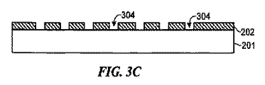
図3Cは、基板201までの溝304を有するレジスト層202だけを残して、オーバーコート層206、成形可能材料204およびレジスト層203が剥がされた後の図3Bの構造物の断面図を示す。特定形状のナノパターンまたは表面フィーチャの形成は、所望のナノ構造に対応する所望の表面パターンが達成されるまで図2A〜図3Cのプロセス・ステップを繰り返すことにより実現されてもよい。
FIG. 3C shows a cross-sectional view of the structure of FIG. 3B after the
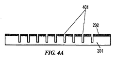
図4Aは、溝401を形成する特定の深さまでエッチングされた図3Cの例示的なパターンの断面図を示す。この図では基板201とレジスト層202が見える。図4Bは、基板201内の溝401の平面図を示す。
FIG. 4A shows a cross-sectional view of the exemplary pattern of FIG. 3C etched to a specific depth to form the
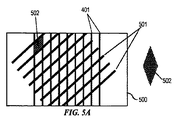
図5Aは、図2A〜図4Bのプロセス・ステップを使用して第1のパターン501を処理した後の基板201の平面図を示す。これにより、このプロセスの順序を使用して菱形表面パターン502が形成されてもよい。トレンチおよび表面パターン502は、構造物500の表面積を大きくするために使用されることがある。
FIG. 5A shows a top view of the
図5Bは、図2A〜図4Bのプロセス・ステップを使用して追加の重ね合わせパターン503により処理した後の基板201の平面図を示す。これにより、このプロセス順序を使用して三角形表面パターン504が形成されてもよい。トレンチおよび表面パターン504は、構造物510の表面積を大きくするために使用されてもよい。別の実施形態では、トレンチは、エッチングされて貫通し、それにより三角形の断面と基板厚さに対応する長さとを有する均一なナノ成形パターンが作成される。
FIG. 5B shows a plan view of the
図6は、ナノ成形構造を有する例示的なナノ成形テンプレートを形成するためのプロセス・ステップの流れ図である。ステップ601で、第1のレジストの薄層が、基板上に付着されてもよい。ステップ602で、第2のレジストのオーバレイが付着されてもよい。例えば、第2のレジストには、湿潤可剥性材料、PMGI(ポリメチルグルタルイミド)などの可溶性材料がある。PMGIは、Shipley Company,L.L.C.(現在のRohm Haas)から商標CD260で入手可能な水酸化テトラメチルアンモニウム(TMAH)によって湿潤剥離されてもよい。あるいは、第2のレジストは、任意のネガフォトレジスト、例えばポリヒドロキシルスチレンでよい。各レジスト層は、米国特許出願公開第2007/0212494号に開示された材料などの接着のための中間層を含んでもよい。ステップ603で、成形可能材料層が、付着されインプリント・モールドでインプリントされて、凹部によってスペースとして分離された隆起パターンのレリーフ・パターンを有する第3のレジスト層が形成されてもよい。一実施形態では、隆起パターンとスペースの幅が等しい。ステップ604で、レリーフ・パターンがエッチングされ、幅に対する高さの比が大きい小さな隆起パターンが形成されてもよい。ステップ605で、隆起線を覆うようにシリコン含有有機材料が塗布されてもよい。一実施形態では、オーバーコート層は、米国特許第7,186,656号に開示されるものと類似のシリコン含有重合体でよい。ステップ606で、全面エッチングによって隆起線の上面が露出されてもよい。ステップ607で、成形可能材料がエッチングされて、異なる化学エッチングに反応する第1のレジスト材料まで下方にトレンチが形成される。ステップ608で、第1のレジスト材料は、基板で停止するようにドライエッチングされてもよい(例えば、酸素で)。ステップ609で、成形可能材料と第2のレジストが、第1のレジストを基板まで下方に貫通するトレンチを残して剥がされてもよい。ステップ610で、基板の表面に形成されたパターンが最終パターンであるかどうか判定されてもよい。ステップ611で、判定がいいえの場合、インプリント・モールドは、重ね合わせパターン、現在パターンの代替および/または既存パターンの回転によって修正されてもよい。例えば、分岐がステップ602に戻されてもよく、プロセス・ステップの一部が繰り返されて、基板の第1のパターンを覆う第2のパターンが形成される。ステップ612で、ステップ610の判定がはいの場合、基板が、パターニングされた第1のレジスト層を介して所望の深さまでエッチングされ、それにより基板上に成形ナノ構造物が形成されてもよい。ステップ613で、第1のレジスト材料が、剥がされてもよい。
FIG. 6 is a flow diagram of process steps for forming an exemplary nanomolded template having a nanomolded structure. In
別の実施形態では、図6は、金属膜(クロムなど)の使用を含んでもよい。例えば、金属膜は、ステップ601に含まれていてもよい。ステップ602は削除されてもよい。ステップ604〜608は、図6にあるようなものでよい。しかしながら、ステップ609は、ハロゲンおよびO2 プラズマ灰化プロセスと置き換えられて、金属膜のエッチング・パターンの後ろにある全ての有機材料が除去されてもよい。このプロセスは、ナノ形状を作成するために必要に応じて何度も繰り返されてもよい。さらに、ステップ603のインプリント処理ステップの直前に任意選択の接着層(前述した)が使用されてもよい。
In another embodiment, FIG. 6 may include the use of a metal film (such as chromium). For example, a metal film may be included in
図6の方法の別の実施形態では、ステップ604〜606は削除されてもよく、ステップ603の成形可能なインプリント材料は、初期ステップで塗布された材料中に直接エッチングされてもよい(湿潤可剥性の第2の材料と非湿潤可剥性の第1の材料か、湿潤可剥性材料なしに使用されるクロムなどの金属膜かにかかわらず)。この実施形態は、図6のプロセス・ステップ603〜606で得られたパターンの逆の調子を有するパターンとなる。
In another embodiment of the method of FIG. 6, steps 604-606 may be omitted and the moldable imprint material of
図6のプロセスの別の実施形態では、ステップ601および602は削除されてもよく、金属膜(例えば、クロム)が、基板上に付着されてもよい。ステップ603の成形可能材料は、インプリントされエッチングされてもよいが、パターンは、基板に直接エッチングされてもよい。ステップ605〜608は削除され、金属膜と基板にトレンチを残して成形可能材料が剥がされてもよい。次に、プロセスは、ナノ形状を作成するために必要に応じて何度も繰り返されてもよい。
In another embodiment of the process of FIG. 6,
図2〜図5は、多くの応用例で有用な成形ナノ構造を有する基板を得るプロセス・ステップを示す。示されたもの以外のナノ構造が、本明細書に述べた方法によって作成されてもよく、本発明の範囲内で検討される。さらに、ナノ構造の形成を支援するために、米国特許第7,186,656号、米国特許第7,252,777号および米国特許第7,261、831号に開示された処理システムおよび方法の要素が使用されてもよく、これらの特許はすべて、参照により本明細書に組み込まれる。 2-5 illustrate process steps for obtaining a substrate with shaped nanostructures useful in many applications. Nanostructures other than those shown may be made by the methods described herein and are contemplated within the scope of the present invention. Further, to assist in the formation of nanostructures, the processing systems and methods disclosed in US Pat. No. 7,186,656, US Pat. No. 7,252,777 and US Pat. No. 7,261,831 Elements may be used and all of these patents are incorporated herein by reference.
図11〜図12に例示的なナノ構造が示される。例えば、図11Aと図11Bは、作成されることがある長方形、正方形、六角形などの形状を示す。三角形や他の非現実的形状を含むがそれらに限定されない他の形状が形成されてもよいことに注意されたい。図11Aでは、第1のパターン1100が、第2のパターン1102と重ね合わされて、少なくとも1つの鋭い縁1108を有する複数のナノ形状1106を有する表面パターン1104を提供してもよい。図11Bでは、第1のパターン1100aが、第2のパターン1102および追加のパターン1102aと重ね合わされてもよい。
Illustrative nanostructures are shown in FIGS. For example, FIGS. 11A and 11B show shapes such as rectangles, squares, and hexagons that may be created. Note that other shapes may be formed, including but not limited to triangles and other unrealistic shapes. In FIG. 11A, a
いくつかの実施形態では、第2のパターン1102および/または追加のパターンが、第1のパターン1100(例えば、パターンの回転)と実質的に類似してもよい。あるいは、第2のパターン1102および/または追加のパターンは、第1のパターン1100と実質的に異なってもよい。例えば、図12Aは第1のパターン1100を示し、図12Bは第2のパターン1102を示す。図12Cに示されたように、第1のパターン110と第2のパターン1102の重なりは、少なくとも1つの鋭い縁1108を有する複数のナノ形状1106を有する表面パターン1104を提供してもよい。
In some embodiments, the
以上の詳細な説明は、最終製品のナノパターンまたはインプリント・モールドを作成するためのナノパターンを実現する方法を述べる。特定のナノパターンの場合、典型的な電子ビーム・プロセスを使用してモールドを直接作成することは実際的でないことがある。その場合、開示されたプロセスを使用して、所望の鋭い角または縁を有する所望のナノパターンを有する第1のインプリント・モールドを作成してもよい。次に、この第1のインプリント・モールドを使用して新しい基板を繰り返しパターニングし、やはり所望の鋭い角または縁を有するより複雑なナノパターンを作成してもよい。所望の複雑なナノパターンは、新しい基板上に実現された後、ステップ・アンド・リピート・プロセスで使用されて、高速でコスト効果の高い生産のための複雑なナノパターンを作成することができる大面積インプリント・モールドが製造される。 The above detailed description describes a method for realizing a nanopattern for producing a final product nanopattern or imprint mold. For certain nanopatterns, it may not be practical to create the mold directly using a typical electron beam process. In that case, the disclosed process may be used to create a first imprint mold having the desired nanopattern with the desired sharp corners or edges. This first imprint mold may then be used to repeatedly pattern a new substrate, creating a more complex nanopattern that also has the desired sharp corners or edges. Once the desired complex nanopattern is realized on a new substrate, it can be used in a step-and-repeat process to create complex nanopatterns for fast and cost-effective production. An area imprint mold is produced.
フェーズ2: ナノパターン構造の複製
図7〜図10は、ナノパターン構造702の例示的な形成の側面図を示す。一般に、図1に関して本明細書で述べたインプリント・リソグラフィ・プロセスを使用してナノパターン構造702を形成するために、重合性材料34が、基板708の表面706に付着され、ナノパターン・モールド700と接触されてもよい。ナノパターン構造702は、残留層712と、少なくとも1つの鋭い縁を有するフィーチャ(例えば、突出部720および/または凹部722)を含んでもよい。残留層712は、厚さtRを有してもよい。薄い残留層712は、ナノパターン構造702の後処理で丸みのあるフィーチャ(例えば、突出部720)の発生を減少させることがある。例えば、残留層712は、丸みのあるフィーチャの発生を減少させるために1〜25nmの厚さtRを有する。
Phase 2 : Nanopatterned Structure Replication FIGS. 7-10 show side views of exemplary formation of
残留層厚さtRは、重合性材料34の体積、表面エネルギーなどによって制御されてもよい。以下の説明では、丸みのあるフィーチャの発生を減少させかつ/または除去しかつ鋭い縁を提供するように残留層厚さtRを制御する方法を概説する。
The residual layer thickness tR may be controlled by the volume of the
体積制御
重合性材料34の体積の選択は、1)液滴体積、2)液滴の広がり、および3)テンプレート容積の3つの特徴によって決定されてもよい。
Volume Control The selection of the volume of the
重合性材料34は、事前に定義された液滴体積を有する低粘性重合性インプリント溶液でよい。重合性材料34の液滴体積は、ナノパターン・モールド700と基板708の接触前に液滴の周囲の高い毛管力によって液滴がどの程度広がるかに基づいて選択されてもよい。例えば、重合性材料34は、0.5〜50cpsの液滴体積を有してもよい。
The
液滴の広がりは、一般に、液滴体積、ナノパターン・モールド700の容積、ナノパターン・モールド700の表面エネルギー、および/または基板708の表面エネルギーの関数である。例えば、ブランク・ナノパターン・モールド700の場合、6plの液滴体積は、分注された液滴の径の約7倍の液滴広がりを提供することがある。この液滴体積は、さらに、10〜15nmの範囲を有する残留層712をもたらすことがある。
Droplet spread is generally a function of drop volume,
一般に、残留層は、さらに、所定の時間中に液滴が広がる領域内のナノパターン・モールド700の容積を超える重合性材料34によって規定されてもよい。場合によって、液滴が広がる単位面積当たりの重合性材料34の体積は、ナノパターン・モールド700の容積よりかなり大きくてもよい。この結果、残留層712が厚くなることがある(例えば、5nm超)。
In general, the residual layer may be further defined by the
表面エネルギーによって、重合性材料34がナノパターン・モールド700と基板708の表面706を濡らすことができ、その結果、重合性材料34が、初期液滴サイズ(すなわち、直径が100μm未満)を超える大きな距離にわたって移動することがある。ナノパターン・モールド700が重合性材料34と接触した後の流体の動きは、毛管作用およびナノパターン・モールド700と基板708との接触形状によって促進されることがある。例えば、液滴は、液滴径の最大6または7倍に広がる均一の膜を形成する。しかしながら、単量体がテンプレート容積を大きく超えないこと、または残留層厚さが5nmを超えることが重要である。
The surface energy allows the
ダミー容積充填フィーチャ
余分な重合性材料34を「吸収」するために、特定のナノパターン・モールド700領域にダミー容積充填フィーチャが導入されてもよい。そのような構造の必要性は、次の式によって決定されることがある。ナノパターン・モールド700のフィーチャ容積が、局部的液滴体積より小さい場合は、5nm未満の残留層厚さtRにダミー充填が必要とされることがある。
変数の定義
r=液滴半径
ri=分注液滴半径
ts=液滴広がり時間
t=時間
Vd=分注液滴体積
Vf=テンプレート・フィーチャ体積
df=テンプレート・フィーチャ深さ
v=格子の場合のテンプレート・デューティ・サイクル
af=フィーチャが占有する面積
RLT=残留層厚さ
ad=液滴広がり面積
Dummy Volume Fill Feature A dummy volume fill feature may be introduced into a
Definition of variables r = droplet radius ri = dispensing drop radius ts = droplet spreading time t = time Vd = dispensing drop volume Vf = template feature volume df = template feature depth v = lattice case Template duty cycle af = area occupied by feature RLT = residual layer thickness ad = droplet spreading area
液滴が格子構造に広がる領域の残留層厚さtRは、次の式によって定義される。 The residual layer thickness t R in the region where the droplet spreads in the lattice structure is defined by the following equation.

残留層厚さtRが正で5nmを超える場合は、所定の広がり面積のVfがほぼ液滴体積になるようにダミー充填が必要とされることがある。残留層厚さtRが負の場合は、追加の重合性材料が加えられてもよい。 When the residual layer thickness t R is positive and exceeds 5 nm, dummy filling may be required so that the Vf of a predetermined spread area becomes substantially the droplet volume. If the residual layer thickness t R is negative, additional polymerizable material may be added.
所定の液滴広がりのフィーチャ面積が小さすぎるか、エッチング深さが浅すぎる場合は、液滴広がり領域内の余分な体積を消費するためにダミー充填が必要とされることがある。液滴広がり面積は、フィーチャの面積と深さの関数であり、重合性材料34の体積が消費されるときの液滴の広がりを制限することがある。
If the feature area for a given drop spread is too small or the etch depth is too shallow, a dummy fill may be required to consume extra volume in the drop spread area. Droplet spread area is a function of feature area and depth and may limit drop spread when the volume of
表面エネルギー
液滴が広がる面積は、重合性材料34とナノパターン・モールド700と基板708の間の表面エネルギー、重合性材料34の粘性、および/または毛管力の関数でよい。毛管力が大きい場合、広がりは素早く起こり、従って低粘性流体と液滴領域内の薄膜を必要とすることがある。
Surface Energy The area over which the droplet spreads may be a function of the surface energy between the
効率的な流体の広がりとフィーチャ充填を可能にするために、ナノパターン・モールド708および/または基板708との重合性材料34の接触角が制御されてもよい。接触角は、定着剤TranspinTMまたはValMatTMを基板708に塗布することにより、また重合性材料34中にナノパターン・モールド700を被覆してもよい界面活性剤を使用することによって制御されてもよい。したがって、重合性材料34のナノパターン・モールド700との接触角は、約500未満でよく、重合性材料34の基板708との接触角は、約150未満でよい。接触角は、表面エネルギーの目安として、ナノパターン・モールド700のフィーチャがナノパターン・モールド700を容易に埋め、また重合性材料34が基板708全体に大きな距離に容易に広がることを可能にすることがある。長距離の広がりは、表面エネルギー、粘性および毛管力によって制御されてもよい。表面エネルギーを制御する能力は、単量体が大きな距離にわたって広がることを可能にすることがある。
The contact angle of the
ナノ形状構造の形成
図7Aと図7Bは、重合性材料34が上に配置された基板708の上に位置決めされたナノパターン・モールド700を示す。ナノパターン・モールド700は、フィーチャ(例えば、凹部714および/または突出部716)を有してもよい。凹部714および/または突出部716は、本明細書で述べたプロセスを使用して鋭い縁を有するように形成されてもよい。例えば、ナノパターン・モールド700は、図7Bに示されたように三角形の凹部714を有するように形成されてもよい。三角形が示されているが、長方形、六角形または他の非現実的形状を含むがこれらに限定されない、鋭い縁とフィーチャを有する任意の形状が形成されてもよいことに注意されたい。
Formation of Nano-Shaped Structure FIGS. 7A and 7B show a
図8〜図9は、高さh1(図8)に位置決めされたナノパターン・モールド700が高さh2(図9)まで移動するとき重合性材料34の広がりを示す。ナノパターン・モールド700は、厚さtNを有してもよい。例えば、ナノパターン・モールド700の厚さは、0.5mm〜10mmの厚さを有する。
FIGS. 8-9 show the spread of the
ナノパターン・モールド700が高さh1から高さh2まで移動する際の重合性材料34の広がりは、一般に、ある程度の追加の印加力によって毛管駆動される。例えば、ナノパターン・モールド700を基板708の上の高さhに位置決めするために、ナノパターン・モールド700上のインプリント・ヘッド38(図1に示された)によって力Fが提供される。しかしながら、力Fは、最小限(例えば、0〜10N)でもよい。さらに、チャック28(図1に示された)は、圧力Pを印加してもよい。また、圧力Pは、実質的な反りや他の実質的な変形なしにナノパターン・モールド700の適切な位置決めを実現するのにまったく十分なことがある。例えば、圧力Pは、約0〜0.1atmでよい。最小印加力(例えば、力Fと圧力P)が、残留層712の変形を減少させることがある。さらに、ナノパターン構造702を形成し分離する際の残留層712の変形を少なくするために、チャック14が基板12に最小力を提供してもよいことに注意されたい。
The spread of the
図10は、厚さtRを有する残留層712と鋭い縁を有する突出部720とを有する形成されたナノパターン構造702を示す。そのような薄い残留層と、接着層が厚さ1nmでよいという事実によって、基板エッチングで始まりディスカム(descum)のないパターン転写が可能になることに注意されたい。この目的のために、インプリント・パターン転写製造プロセスは、接着層(厚さ1nm)の蒸気被覆、ドロップオンデマンドのレジスト分注(分注パターンと単量体体積はテンプレート容積の計算に基づく)、5nm未満のRLTと基板のみのエッチング(ディスカムなし)によるインプリント・パターニング(必要に応じてダミー充填)、剥がし、および基板クリーニングを含んでもよい。ディスカム・エッチングが必要な場合は、それは、薄い残留膜を除去するためのものでよく、したがって形成されたナノ構造物の形状に実質的に影響しなくてもよいことに注意されたい。これにより、モールド内にあるナノ形状を保持したまま基板のエッチングが可能になることがある。これは、接着層(厚さ1nm)の蒸気被覆、インプリント材料の回転塗布、5nm未満のRLTのインプリント・パターニング、実質的にインプリント・レジストのディスカム(O2プラズマによる)、基板エッチング、剥がし、基板クリーニングが行われる従来のインプリント・リソグラフィと対照的である。
FIG. 10 shows a formed
以上述べた本明細書の実施形態は例示的である。上記の開示に対して本発明の範囲内にある多くの変更と修正が行われてもよい。したがって、本発明の範囲は、以上の説明によって限定されるべきでなく、むしろ添付の特許請求の範囲をその等価物の全範囲と共に参照することにより、決定されるべきである。 The embodiments described herein are exemplary. Many changes and modifications within the scope of the present invention may be made to the above disclosure. Accordingly, the scope of the invention should not be limited by the foregoing description, but rather should be determined by reference to the appended claims, along with their full scope of equivalents.
401…溝、500…構造物、501…パターン、502…表面パターン。 401 ... groove, 500 ... structure, 501 ... pattern, 502 ... surface pattern.
Claims (15)
前記第1の層の前記第1のパターンに重なる第2のパターンを形成するステップと、
前記第1のパターンと前記第2のパターンを前記基板にエッチングし、少なくとも1つの鋭い縁を有する複数のフィーチャを含む表面パターンを有するナノ成形インプリント・リソグラフィ・テンプレートへと形成するステップと、
から構成され、
前記第1の層は、ドライエッチング可能な、かつ、実質的に湿潤剥離(wet-strip)されないレジスト材料から形成されることを特徴とする方法。 Forming a first pattern including grooves in a first layer of material disposed on a substrate;
Forming a second pattern overlying the first pattern of the first layer;
Etching the first pattern and the second pattern into the substrate to form a nano-molded imprint lithography template having a surface pattern comprising a plurality of features having at least one sharp edge;
Consisting of
The method is characterized in that the first layer is formed from a resist material that is dry-etchable and substantially not wet-striped .
前記第1の層上に第2の湿潤可剥性レジスト層を付着させるステップと、
前記第2の湿潤可剥性レジスト層上に成形可能材料を付着させるステップと、
ナノインプリント・リソグラフィ・テンプレートを使用して前記成形可能材料をインプリントして、凹部によって分離された複数の隆起部分を有する第1のパターン層を有する第3のレジスト層を形成するステップと、
前記第3のレジスト層を、前記隆起部分の高さ対幅比が実質的に大きくなるようにエッチングするステップと、
前記第3のレジスト層上にオーバーコート層を付着させ、前記オーバーコート層を平坦化して各隆起部分の縁を露出させるステップと、
前記第3のレジスト層をエッチングして、前記第2の湿潤可剥性レジスト層と前記第1の層に1つまたは複数のトレンチを形成するステップと、
前記第2の湿潤可剥性レジスト層と前記第3のレジスト層を除去するステップと
を含むことを特徴とする請求項1に記載の方法。 Forming the first pattern comprises:
Depositing a second wet strippable resist layer on the first layer;
Depositing a moldable material on the second wet strippable resist layer;
Imprinting the moldable material using a nanoimprint lithography template to form a third resist layer having a first patterned layer having a plurality of raised portions separated by recesses;
Etching the third resist layer such that a height to width ratio of the raised portion is substantially increased;
Depositing an overcoat layer on the third resist layer and planarizing the overcoat layer to expose the edges of each raised portion;
Etching the third resist layer to form one or more trenches in the second wet strippable resist layer and the first layer;
The method of claim 1, comprising removing the second wet strippable resist layer and the third resist layer.
前記第1の層上に第2の湿潤可剥性レジスト層を付着させるステップと、
前記第2の湿潤可剥性レジスト層上に成形可能材料を付着させるステップと、
ナノインプリント・リソグラフィ・テンプレートを使用して前記成形可能材料をインプリントして、凹部によって分離された複数の隆起部分を含む第1のパターン層を有する第3のレジスト層を形成するステップと、
前記第3のレジスト層をエッチングして前記第2の湿潤可剥性レジスト層と前記第1の層に1つまたは複数のトレンチを形成するステップと、
前記第2の湿潤可剥性レジスト層と前記第3のレジスト層を除去するステップと、
を含むことを特徴とする請求項1、請求項3乃至12のいずれか1項に記載の方法。 The first layer is formed of a resist material that can be dry-etched, and the step of forming the first pattern includes:
Depositing a second wet strippable resist layer on the first layer;
Depositing a moldable material on the second wet strippable resist layer;
Imprinting the moldable material using a nanoimprint lithography template to form a third resist layer having a first patterned layer comprising a plurality of raised portions separated by recesses;
Etching the third resist layer to form one or more trenches in the second wet strippable resist layer and the first layer;
Removing the second wet strippable resist layer and the third resist layer;
The method according to any one of claims 1 and 3 to 12, characterized by comprising:
前記第1の層上に成形可能材料を付着させるステップと、
ナノインプリント・リソグラフィ・テンプレートを使用して前記成形可能材料をインプリントして、凹部によって分離された複数の隆起部分を含む第1のパターン層を有する第2のレジスト層を形成するステップと、
前記第2のレジスト層をエッチングして前記第1の層に1つまたは複数のトレンチを形成するステップと、
前記第1の層にエッチング・パターンが提供されるようにすべての有機材料を除去するステップと、
を含むことを特徴とする請求項2に記載の方法。 Forming the first pattern comprises:
Depositing a moldable material on the first layer;
Imprinting the moldable material using a nanoimprint lithography template to form a second resist layer having a first patterned layer comprising a plurality of raised portions separated by recesses;
Forming one or more trenches on the first layer by etching the second les resist layer,
Removing all organic material such that an etching pattern is provided in the first layer;
The method of claim 2 comprising:
Applications Claiming Priority (5)
| Application Number | Priority Date | Filing Date | Title |
|---|---|---|---|
| US11423908P | 2008-11-13 | 2008-11-13 | |
| US61/114,239 | 2008-11-13 | ||
| US12/616,896 US8529778B2 (en) | 2008-11-13 | 2009-11-12 | Large area patterning of nano-sized shapes |
| US12/616,896 | 2009-11-12 | ||
| PCT/US2009/006113 WO2010056349A2 (en) | 2008-11-13 | 2009-11-13 | Large area patterning of nano-sized shapes |
Publications (3)
| Publication Number | Publication Date |
|---|---|
| JP2012508978A JP2012508978A (en) | 2012-04-12 |
| JP2012508978A5 JP2012508978A5 (en) | 2012-12-27 |
| JP5723779B2 true JP5723779B2 (en) | 2015-05-27 |
Family
ID=42165606
Family Applications (1)
| Application Number | Title | Priority Date | Filing Date |
|---|---|---|---|
| JP2011536331A Active JP5723779B2 (en) | 2008-11-13 | 2009-11-13 | Large area patterning of nano size shape |
Country Status (5)
| Country | Link |
|---|---|
| US (2) | US8529778B2 (en) |
| EP (1) | EP2344926B1 (en) |
| JP (1) | JP5723779B2 (en) |
| TW (1) | TWI453106B (en) |
| WO (1) | WO2010056349A2 (en) |
Cited By (1)
| Publication number | Priority date | Publication date | Assignee | Title |
|---|---|---|---|---|
| US9585439B2 (en) | 2011-10-28 | 2017-03-07 | D B Industries, Llc | Connector |
Families Citing this family (22)
| Publication number | Priority date | Publication date | Assignee | Title |
|---|---|---|---|---|
| US20110048518A1 (en) * | 2009-08-26 | 2011-03-03 | Molecular Imprints, Inc. | Nanostructured thin film inorganic solar cells |
| EP2470956B1 (en) * | 2009-08-26 | 2018-02-14 | Molecular Imprints, Inc. | Functional nanoparticles |
| KR101274715B1 (en) * | 2009-12-22 | 2013-06-12 | 엘지디스플레이 주식회사 | Thin film transistor substrate and method of fabricating the same |
| JP2013517943A (en) | 2010-01-29 | 2013-05-20 | モレキュラー・インプリンツ・インコーポレーテッド | Nanoimprint lithography process to form nanoparticles |
| JP2013538447A (en) | 2010-08-05 | 2013-10-10 | エーエスエムエル ネザーランズ ビー.ブイ. | Imprint lithography |
| WO2012033943A2 (en) * | 2010-09-08 | 2012-03-15 | Molecular Imprints, Inc. | Vapor delivery system for use in imprint lithography |
| CN103282303A (en) | 2010-11-05 | 2013-09-04 | 分子制模股份有限公司 | Nanoimprint lithography formation of functional nanoparticles using dual release layers |
| US8828297B2 (en) | 2010-11-05 | 2014-09-09 | Molecular Imprints, Inc. | Patterning of non-convex shaped nanostructures |
| TWI400160B (en) * | 2010-11-18 | 2013-07-01 | Univ Nat Taiwan Science Tech | A micro/nano-imprint mold of the fabricating process |
| US20130167916A1 (en) * | 2011-12-28 | 2013-07-04 | Taiwan Semiconductor Manufacturing Co., Ltd. | Thin film photovoltaic cells and methods of forming the same |
| CN103018819B (en) * | 2012-11-09 | 2014-05-21 | 浙江大学 | Method for preparing high polymer micro-nano fiber bragg grating based on nanoimprint lithography |
| JP6135119B2 (en) * | 2012-12-19 | 2017-05-31 | 大日本印刷株式会社 | Imprint method, imprint resin dripping position determination method, and imprint apparatus |
| JP6171424B2 (en) * | 2013-03-12 | 2017-08-02 | 大日本印刷株式会社 | Manufacturing method and design method of imprint mold |
| WO2014144133A1 (en) * | 2013-03-15 | 2014-09-18 | The Trustees Of The Princeton University | Analyte detection enhancement by targeted immobilization, surface amplification, and pixelated reading and analysis |
| WO2015006695A1 (en) * | 2013-07-12 | 2015-01-15 | Canon Nanotechnologies, Inc. | Drop pattern generation for imprint lithography with directionally-patterned templates |
| KR101427160B1 (en) * | 2014-04-07 | 2014-08-07 | 서울과학기술대학교 산학협력단 | Device for Multi Micro-Pattern Forming and Method Thereof |
| JP6279430B2 (en) * | 2014-08-21 | 2018-02-14 | 東芝メモリ株式会社 | Template, template forming method, and semiconductor device manufacturing method |
| US10349424B2 (en) * | 2015-11-05 | 2019-07-09 | Gainspan Corporation | Efficient dual-mode operation of a wireless device as an access point and a wireless station of respective WLAN networks |
| US10484954B2 (en) * | 2017-05-10 | 2019-11-19 | Qualcomm Incorporated | Synchronization for wideband coverage enhancement |
| US10609660B2 (en) * | 2017-04-19 | 2020-03-31 | Qualcomm Incorporated | Synchronization for wideband coverage enhancement |
| JP6447657B2 (en) * | 2017-04-25 | 2019-01-09 | 大日本印刷株式会社 | Imprint resin dripping order determination method and imprint method |
| US10942398B1 (en) * | 2017-05-19 | 2021-03-09 | Facebook Technologies, Llc | Continuous liquid crystal alignment patterns for geometric phase optics |
Family Cites Families (50)
| Publication number | Priority date | Publication date | Assignee | Title |
|---|---|---|---|---|
| CN100504598C (en) | 2000-07-16 | 2009-06-24 | 得克萨斯州大学系统董事会 | High-resolution overlay alignment methods and systems for imprint lithography |
| CN100365507C (en) | 2000-10-12 | 2008-01-30 | 德克萨斯州大学系统董事会 | Template for room temperature, low pressure micro-and nano-imprint lithography |
| JP3589201B2 (en) * | 2001-07-02 | 2004-11-17 | Tdk株式会社 | Thin film patterning method, thin film device manufacturing method, and thin film magnetic head manufacturing method |
| US20050064344A1 (en) | 2003-09-18 | 2005-03-24 | University Of Texas System Board Of Regents | Imprint lithography templates having alignment marks |
| US7144539B2 (en) | 2002-04-04 | 2006-12-05 | Obducat Ab | Imprint method and device |
| US7037639B2 (en) | 2002-05-01 | 2006-05-02 | Molecular Imprints, Inc. | Methods of manufacturing a lithography template |
| US7179079B2 (en) | 2002-07-08 | 2007-02-20 | Molecular Imprints, Inc. | Conforming template for patterning liquids disposed on substrates |
| US6900881B2 (en) | 2002-07-11 | 2005-05-31 | Molecular Imprints, Inc. | Step and repeat imprint lithography systems |
| US7077992B2 (en) | 2002-07-11 | 2006-07-18 | Molecular Imprints, Inc. | Step and repeat imprint lithography processes |
| US6916584B2 (en) | 2002-08-01 | 2005-07-12 | Molecular Imprints, Inc. | Alignment methods for imprint lithography |
| US7070405B2 (en) | 2002-08-01 | 2006-07-04 | Molecular Imprints, Inc. | Alignment systems for imprint lithography |
| US7027156B2 (en) | 2002-08-01 | 2006-04-11 | Molecular Imprints, Inc. | Scatterometry alignment for imprint lithography |
| US8349241B2 (en) * | 2002-10-04 | 2013-01-08 | Molecular Imprints, Inc. | Method to arrange features on a substrate to replicate features having minimal dimensional variability |
| US7378347B2 (en) * | 2002-10-28 | 2008-05-27 | Hewlett-Packard Development Company, L.P. | Method of forming catalyst nanoparticles for nanowire growth and other applications |
| US7179396B2 (en) | 2003-03-25 | 2007-02-20 | Molecular Imprints, Inc. | Positive tone bi-layer imprint lithography method |
| US7186656B2 (en) | 2004-05-21 | 2007-03-06 | Molecular Imprints, Inc. | Method of forming a recessed structure employing a reverse tone process |
| US7323417B2 (en) * | 2004-09-21 | 2008-01-29 | Molecular Imprints, Inc. | Method of forming a recessed structure employing a reverse tone process |
| US7136150B2 (en) | 2003-09-25 | 2006-11-14 | Molecular Imprints, Inc. | Imprint lithography template having opaque alignment marks |
| US20050084804A1 (en) | 2003-10-16 | 2005-04-21 | Molecular Imprints, Inc. | Low surface energy templates |
| JP2005150333A (en) * | 2003-11-14 | 2005-06-09 | Sony Corp | Method of manufacturing semiconductor device |
| US20050189676A1 (en) | 2004-02-27 | 2005-09-01 | Molecular Imprints, Inc. | Full-wafer or large area imprinting with multiple separated sub-fields for high throughput lithography |
| US20050230882A1 (en) | 2004-04-19 | 2005-10-20 | Molecular Imprints, Inc. | Method of forming a deep-featured template employed in imprint lithography |
| US7785526B2 (en) | 2004-07-20 | 2010-08-31 | Molecular Imprints, Inc. | Imprint alignment method, system, and template |
| US7309225B2 (en) | 2004-08-13 | 2007-12-18 | Molecular Imprints, Inc. | Moat system for an imprint lithography template |
| US7252777B2 (en) | 2004-09-21 | 2007-08-07 | Molecular Imprints, Inc. | Method of forming an in-situ recessed structure |
| JP5167583B2 (en) * | 2004-11-10 | 2013-03-21 | 東レ株式会社 | Pattern forming method and pattern forming sheet |
| WO2006060757A2 (en) | 2004-12-01 | 2006-06-08 | Molecular Imprints, Inc. | Eliminating printability of sub-resolution defects in imprint lithography |
| EP1891479B1 (en) * | 2005-05-10 | 2014-04-09 | Dow Corning Corporation | Sub-micron decal transfer lithography |
| US8808808B2 (en) | 2005-07-22 | 2014-08-19 | Molecular Imprints, Inc. | Method for imprint lithography utilizing an adhesion primer layer |
| US8557351B2 (en) * | 2005-07-22 | 2013-10-15 | Molecular Imprints, Inc. | Method for adhering materials together |
| JP2007069604A (en) * | 2005-08-10 | 2007-03-22 | Toray Ind Inc | Pattern forming method, pattern forming sheet and optically functional sheet formed using it |
| WO2008060266A2 (en) | 2005-10-03 | 2008-05-22 | Massachusetts Institute Of Technology | Nanotemplate arbitrary-imprint lithography |
| US8636937B2 (en) * | 2005-10-20 | 2014-01-28 | Agency For Science, Technology And Research | Hierarchical nanopatterns by nanoimprint lithography |
| US7759253B2 (en) | 2006-08-07 | 2010-07-20 | Taiwan Semiconductor Manufacturing Company, Ltd. | Method and material for forming a double exposure lithography pattern |
| US8142850B2 (en) | 2006-04-03 | 2012-03-27 | Molecular Imprints, Inc. | Patterning a plurality of fields on a substrate to compensate for differing evaporation times |
| KR20090003153A (en) | 2006-04-03 | 2009-01-09 | 몰레큘러 임프린츠 인코퍼레이티드 | Method of concurrently patterning a substrate having a plurality of fields and alignment marks |
| US7341825B2 (en) | 2006-05-25 | 2008-03-11 | Hitachi Global Storage Technologies Netherlands B.V. | Method for producing high resolution nano-imprinting masters |
| TW200818257A (en) * | 2006-07-06 | 2008-04-16 | Nxp Bv | Imprint lithography |
| JP4580017B2 (en) * | 2006-10-20 | 2010-11-10 | 富士通株式会社 | Pattern transfer stamper, magnetic recording medium manufacturing method using the same, and magnetic recording medium |
| US7758981B2 (en) * | 2007-07-25 | 2010-07-20 | Hitachi Global Storage Technologies Netherlands B.V. | Method for making a master disk for nanoimprinting patterned magnetic recording disks, master disk made by the method, and disk imprinted by the master disk |
| JP4445538B2 (en) * | 2007-09-26 | 2010-04-07 | 株式会社東芝 | Pattern formation method |
| JP2009107128A (en) * | 2007-10-26 | 2009-05-21 | Hitachi Maxell Ltd | Method for producing mold for molding well plate, mold for molding well plate, method for molding well plate using this mold, and well plate |
| US7906274B2 (en) | 2007-11-21 | 2011-03-15 | Molecular Imprints, Inc. | Method of creating a template employing a lift-off process |
| WO2009085286A1 (en) | 2007-12-28 | 2009-07-09 | Molecular Imprints, Inc. | Template pattern density doubling |
| US20090212012A1 (en) | 2008-02-27 | 2009-08-27 | Molecular Imprints, Inc. | Critical dimension control during template formation |
| US8119017B2 (en) * | 2008-06-17 | 2012-02-21 | Hitachi Global Storage Technologies Netherlands B.V. | Method using block copolymers for making a master mold with high bit-aspect-ratio for nanoimprinting patterned magnetic recording disks |
| US20100015270A1 (en) | 2008-07-15 | 2010-01-21 | Molecular Imprints, Inc. | Inner cavity system for nano-imprint lithography |
| US20100095862A1 (en) | 2008-10-22 | 2010-04-22 | Molecular Imprints, Inc. | Double Sidewall Angle Nano-Imprint Template |
| US8877073B2 (en) | 2008-10-27 | 2014-11-04 | Canon Nanotechnologies, Inc. | Imprint lithography template |
| US9122148B2 (en) | 2008-11-03 | 2015-09-01 | Canon Nanotechnologies, Inc. | Master template replication |
-
2009
- 2009-11-12 US US12/616,896 patent/US8529778B2/en active Active
- 2009-11-13 TW TW098138626A patent/TWI453106B/en active
- 2009-11-13 JP JP2011536331A patent/JP5723779B2/en active Active
- 2009-11-13 WO PCT/US2009/006113 patent/WO2010056349A2/en active Application Filing
- 2009-11-13 EP EP09756590.7A patent/EP2344926B1/en active Active
-
2013
- 2013-09-09 US US14/021,463 patent/US20140021167A1/en not_active Abandoned
Cited By (1)
| Publication number | Priority date | Publication date | Assignee | Title |
|---|---|---|---|---|
| US9585439B2 (en) | 2011-10-28 | 2017-03-07 | D B Industries, Llc | Connector |
Also Published As
| Publication number | Publication date |
|---|---|
| WO2010056349A2 (en) | 2010-05-20 |
| EP2344926A2 (en) | 2011-07-20 |
| US8529778B2 (en) | 2013-09-10 |
| EP2344926B1 (en) | 2015-07-01 |
| WO2010056349A3 (en) | 2010-11-11 |
| US20100120251A1 (en) | 2010-05-13 |
| TWI453106B (en) | 2014-09-21 |
| US20140021167A1 (en) | 2014-01-23 |
| JP2012508978A (en) | 2012-04-12 |
| TW201026474A (en) | 2010-07-16 |
Similar Documents
| Publication | Publication Date | Title |
|---|---|---|
| JP5723779B2 (en) | Large area patterning of nano size shape | |
| JP4838108B2 (en) | Imprint lithography | |
| TWI380895B (en) | Controlling thickness of residual layer | |
| JP5982386B2 (en) | Pattern formation of non-convex nanostructures | |
| Lan et al. | Nanoimprint lithography | |
| JP5404654B2 (en) | Limit dimension control during template formation | |
| Peroz et al. | Step and repeat UV nanoimprint lithography on pre-spin coated resist film: a promising route for fabricating nanodevices | |
| WO2008082650A1 (en) | Imprint fluid control | |
| JP6596136B2 (en) | Nanoimprint template using light-shielding material and manufacturing method | |
| WO2008097278A2 (en) | Etch-enhanced technique for lift-off patterning | |
| US20100095862A1 (en) | Double Sidewall Angle Nano-Imprint Template | |
| KR20130105661A (en) | High contrast alignment marks through multiple stage imprinting | |
| EP2901212B1 (en) | Method for fabrication of nano-structures | |
| KR20150100610A (en) | Method for producing nanoimprint mold | |
| JP2013202900A (en) | Mold and method of manufacturing the same, nanoimprint method, and method of manufacturing patterned substrate | |
| US20070249175A1 (en) | Pitch-shrinking technologies for lithographic application | |
| JP2009194170A (en) | Micro pattern forming method | |
| US20230205080A1 (en) | Template, method of forming a template, apparatus and method of manufacturing an article | |
| JP5915027B2 (en) | Pattern forming structure and fine pattern forming method | |
| JP6171453B2 (en) | Manufacturing method of nanoimprint mold | |
| LaBrake et al. | Large area patterning of nano-sized shapes |
Legal Events
| Date | Code | Title | Description |
|---|---|---|---|
| A521 | Request for written amendment filed |
Free format text: JAPANESE INTERMEDIATE CODE: A523 Effective date: 20121106 |
|
| A621 | Written request for application examination |
Free format text: JAPANESE INTERMEDIATE CODE: A621 Effective date: 20121106 |
|
| A977 | Report on retrieval |
Free format text: JAPANESE INTERMEDIATE CODE: A971007 Effective date: 20131226 |
|
| A131 | Notification of reasons for refusal |
Free format text: JAPANESE INTERMEDIATE CODE: A131 Effective date: 20140212 |
|
| A521 | Request for written amendment filed |
Free format text: JAPANESE INTERMEDIATE CODE: A523 Effective date: 20140512 |
|
| A131 | Notification of reasons for refusal |
Free format text: JAPANESE INTERMEDIATE CODE: A131 Effective date: 20141104 |
|
| A521 | Request for written amendment filed |
Free format text: JAPANESE INTERMEDIATE CODE: A523 Effective date: 20150204 |
|
| TRDD | Decision of grant or rejection written | ||
| A01 | Written decision to grant a patent or to grant a registration (utility model) |
Free format text: JAPANESE INTERMEDIATE CODE: A01 Effective date: 20150303 |
|
| A61 | First payment of annual fees (during grant procedure) |
Free format text: JAPANESE INTERMEDIATE CODE: A61 Effective date: 20150330 |
|
| R150 | Certificate of patent or registration of utility model |
Ref document number: 5723779 Country of ref document: JP Free format text: JAPANESE INTERMEDIATE CODE: R150 |
|
| R250 | Receipt of annual fees |
Free format text: JAPANESE INTERMEDIATE CODE: R250 |
|
| R250 | Receipt of annual fees |
Free format text: JAPANESE INTERMEDIATE CODE: R250 |
|
| R250 | Receipt of annual fees |
Free format text: JAPANESE INTERMEDIATE CODE: R250 |
|
| R250 | Receipt of annual fees |
Free format text: JAPANESE INTERMEDIATE CODE: R250 |
|
| R250 | Receipt of annual fees |
Free format text: JAPANESE INTERMEDIATE CODE: R250 |
|
| R250 | Receipt of annual fees |
Free format text: JAPANESE INTERMEDIATE CODE: R250 |
|
| R250 | Receipt of annual fees |
Free format text: JAPANESE INTERMEDIATE CODE: R250 |