JP5708625B2 - Power storage system - Google Patents
Power storage system Download PDFInfo
- Publication number
- JP5708625B2 JP5708625B2 JP2012264010A JP2012264010A JP5708625B2 JP 5708625 B2 JP5708625 B2 JP 5708625B2 JP 2012264010 A JP2012264010 A JP 2012264010A JP 2012264010 A JP2012264010 A JP 2012264010A JP 5708625 B2 JP5708625 B2 JP 5708625B2
- Authority
- JP
- Japan
- Prior art keywords
- circuit
- power storage
- voltage value
- current
- alarm
- Prior art date
- Legal status (The legal status is an assumption and is not a legal conclusion. Google has not performed a legal analysis and makes no representation as to the accuracy of the status listed.)
- Active
Links
Images


Classifications
-
- H—ELECTRICITY
- H02—GENERATION; CONVERSION OR DISTRIBUTION OF ELECTRIC POWER
- H02J—CIRCUIT ARRANGEMENTS OR SYSTEMS FOR SUPPLYING OR DISTRIBUTING ELECTRIC POWER; SYSTEMS FOR STORING ELECTRIC ENERGY
- H02J7/00—Circuit arrangements for charging or depolarising batteries or for supplying loads from batteries
- H02J7/0029—Circuit arrangements for charging or depolarising batteries or for supplying loads from batteries with safety or protection devices or circuits
- H02J7/0031—Circuit arrangements for charging or depolarising batteries or for supplying loads from batteries with safety or protection devices or circuits using battery or load disconnect circuits
-
- B—PERFORMING OPERATIONS; TRANSPORTING
- B60—VEHICLES IN GENERAL
- B60L—PROPULSION OF ELECTRICALLY-PROPELLED VEHICLES; SUPPLYING ELECTRIC POWER FOR AUXILIARY EQUIPMENT OF ELECTRICALLY-PROPELLED VEHICLES; ELECTRODYNAMIC BRAKE SYSTEMS FOR VEHICLES IN GENERAL; MAGNETIC SUSPENSION OR LEVITATION FOR VEHICLES; MONITORING OPERATING VARIABLES OF ELECTRICALLY-PROPELLED VEHICLES; ELECTRIC SAFETY DEVICES FOR ELECTRICALLY-PROPELLED VEHICLES
- B60L58/00—Methods or circuit arrangements for monitoring or controlling batteries or fuel cells, specially adapted for electric vehicles
- B60L58/10—Methods or circuit arrangements for monitoring or controlling batteries or fuel cells, specially adapted for electric vehicles for monitoring or controlling batteries
- B60L58/12—Methods or circuit arrangements for monitoring or controlling batteries or fuel cells, specially adapted for electric vehicles for monitoring or controlling batteries responding to state of charge [SoC]
- B60L58/15—Preventing overcharging
-
- H—ELECTRICITY
- H02—GENERATION; CONVERSION OR DISTRIBUTION OF ELECTRIC POWER
- H02J—CIRCUIT ARRANGEMENTS OR SYSTEMS FOR SUPPLYING OR DISTRIBUTING ELECTRIC POWER; SYSTEMS FOR STORING ELECTRIC ENERGY
- H02J7/00—Circuit arrangements for charging or depolarising batteries or for supplying loads from batteries
- H02J7/0013—Circuit arrangements for charging or depolarising batteries or for supplying loads from batteries acting upon several batteries simultaneously or sequentially
- H02J7/0014—Circuits for equalisation of charge between batteries
-
- H—ELECTRICITY
- H02—GENERATION; CONVERSION OR DISTRIBUTION OF ELECTRIC POWER
- H02J—CIRCUIT ARRANGEMENTS OR SYSTEMS FOR SUPPLYING OR DISTRIBUTING ELECTRIC POWER; SYSTEMS FOR STORING ELECTRIC ENERGY
- H02J7/00—Circuit arrangements for charging or depolarising batteries or for supplying loads from batteries
- H02J7/0029—Circuit arrangements for charging or depolarising batteries or for supplying loads from batteries with safety or protection devices or circuits
- H02J7/00302—Overcharge protection
-
- H—ELECTRICITY
- H02—GENERATION; CONVERSION OR DISTRIBUTION OF ELECTRIC POWER
- H02J—CIRCUIT ARRANGEMENTS OR SYSTEMS FOR SUPPLYING OR DISTRIBUTING ELECTRIC POWER; SYSTEMS FOR STORING ELECTRIC ENERGY
- H02J7/00—Circuit arrangements for charging or depolarising batteries or for supplying loads from batteries
- H02J7/0029—Circuit arrangements for charging or depolarising batteries or for supplying loads from batteries with safety or protection devices or circuits
- H02J7/00306—Overdischarge protection
-
- H—ELECTRICITY
- H02—GENERATION; CONVERSION OR DISTRIBUTION OF ELECTRIC POWER
- H02J—CIRCUIT ARRANGEMENTS OR SYSTEMS FOR SUPPLYING OR DISTRIBUTING ELECTRIC POWER; SYSTEMS FOR STORING ELECTRIC ENERGY
- H02J7/00—Circuit arrangements for charging or depolarising batteries or for supplying loads from batteries
- H02J7/0029—Circuit arrangements for charging or depolarising batteries or for supplying loads from batteries with safety or protection devices or circuits
- H02J7/00308—Overvoltage protection
-
- H—ELECTRICITY
- H02—GENERATION; CONVERSION OR DISTRIBUTION OF ELECTRIC POWER
- H02J—CIRCUIT ARRANGEMENTS OR SYSTEMS FOR SUPPLYING OR DISTRIBUTING ELECTRIC POWER; SYSTEMS FOR STORING ELECTRIC ENERGY
- H02J7/00—Circuit arrangements for charging or depolarising batteries or for supplying loads from batteries
- H02J7/34—Parallel operation in networks using both storage and other dc sources, e.g. providing buffering
- H02J7/345—Parallel operation in networks using both storage and other dc sources, e.g. providing buffering using capacitors as storage or buffering devices
-
- Y—GENERAL TAGGING OF NEW TECHNOLOGICAL DEVELOPMENTS; GENERAL TAGGING OF CROSS-SECTIONAL TECHNOLOGIES SPANNING OVER SEVERAL SECTIONS OF THE IPC; TECHNICAL SUBJECTS COVERED BY FORMER USPC CROSS-REFERENCE ART COLLECTIONS [XRACs] AND DIGESTS
- Y02—TECHNOLOGIES OR APPLICATIONS FOR MITIGATION OR ADAPTATION AGAINST CLIMATE CHANGE
- Y02T—CLIMATE CHANGE MITIGATION TECHNOLOGIES RELATED TO TRANSPORTATION
- Y02T10/00—Road transport of goods or passengers
- Y02T10/60—Other road transportation technologies with climate change mitigation effect
- Y02T10/62—Hybrid vehicles
-
- Y—GENERAL TAGGING OF NEW TECHNOLOGICAL DEVELOPMENTS; GENERAL TAGGING OF CROSS-SECTIONAL TECHNOLOGIES SPANNING OVER SEVERAL SECTIONS OF THE IPC; TECHNICAL SUBJECTS COVERED BY FORMER USPC CROSS-REFERENCE ART COLLECTIONS [XRACs] AND DIGESTS
- Y02—TECHNOLOGIES OR APPLICATIONS FOR MITIGATION OR ADAPTATION AGAINST CLIMATE CHANGE
- Y02T—CLIMATE CHANGE MITIGATION TECHNOLOGIES RELATED TO TRANSPORTATION
- Y02T10/00—Road transport of goods or passengers
- Y02T10/60—Other road transportation technologies with climate change mitigation effect
- Y02T10/70—Energy storage systems for electromobility, e.g. batteries
Description
本発明は、コントローラの制御(プログラム制御)に関わらず、蓄電装置の通電を遮断する技術に関する。 The present invention relates to a technique for interrupting energization of a power storage device regardless of controller control (program control).
二次電池の過充電を抑制するために、二次電池に充電電流が流れたときには、システムメインリレーをオフにする技術が提案されている。システムメインリレーをオフにすることにより、二次電池および負荷の接続を遮断することができ、二次電池の充電を停止することができ、二次電池の過充電を抑制することができる。 In order to suppress the overcharge of the secondary battery, a technique for turning off the system main relay when a charging current flows through the secondary battery has been proposed. By turning off the system main relay, the connection between the secondary battery and the load can be cut off, charging of the secondary battery can be stopped, and overcharging of the secondary battery can be suppressed.
システムメインリレーのオン/オフ制御は、ECU(Electric Control Unit)に含まれるCPU(Central Processing Unit)によって行われる。CPUは、システムメインリレーの駆動制御だけでなく、他の制御も行っており、CPUに含まれるプログラムを変更することがある。ここで、プログラムを変更するときには、プログラムの変更後において、システムメインリレーの駆動制御、言い換えれば、過充電を抑制する制御が正常に行われるか否かを検査しなければならない。 On / off control of the system main relay is performed by a CPU (Central Processing Unit) included in an ECU (Electric Control Unit). The CPU performs not only the drive control of the system main relay but also other controls, and the program included in the CPU may be changed. Here, when the program is changed, it is necessary to check whether or not the drive control of the system main relay, in other words, the control for suppressing the overcharge is normally performed after the change of the program.
本発明である蓄電システムは、複数の蓄電ブロックが直列に接続された蓄電装置と、リレーと、コントローラと、電流遮断回路とを有する。リレーは、蓄電装置および負荷を接続するオンと、蓄電装置および負荷の接続を遮断するオフとの間で切り替わる。コントローラは、リレーのオンおよびオフを制御する。電流遮断回路は、リレーをオンからオフに切り替えて、蓄電ブロックの通電を遮断する。 The power storage system according to the present invention includes a power storage device in which a plurality of power storage blocks are connected in series, a relay, a controller, and a current interrupt circuit. The relay switches between ON for connecting the power storage device and the load and OFF for disconnecting the connection between the power storage device and the load. The controller controls ON and OFF of the relay. The current interrupt circuit switches the relay from on to off and interrupts energization of the storage block.
電流遮断回路は、アラーム回路と、ラッチ回路と、トランジスタとを有する。アラーム回路は、入力される各蓄電ブロックの電圧値および閾値を比較して、蓄電ブロックが過充電状態又は過放電状態であることを示すアラーム信号を出力する。ラッチ回路は、アラーム信号を保持し、保持した信号を出力する。トランジスタは、ラッチ回路の出力信号を受けて、リレーをオンからオフに切り替える。コントローラは、アラーム回路に入力される電圧値又は閾値を変更して、アラーム回路からアラーム信号を出力させる制御を行った後に、蓄電装置の通電状態を判別する。 The current interrupt circuit includes an alarm circuit, a latch circuit, and a transistor. The alarm circuit compares the input voltage value and threshold value of each power storage block, and outputs an alarm signal indicating that the power storage block is in an overcharge state or an overdischarge state. The latch circuit holds the alarm signal and outputs the held signal. The transistor receives the output signal of the latch circuit and switches the relay from on to off. The controller changes the voltage value or threshold value input to the alarm circuit and performs control to output an alarm signal from the alarm circuit, and then determines the energization state of the power storage device.
蓄電ブロックは、充放電を行う蓄電素子で構成することができる。具体的には、蓄電ブロックは、1つの蓄電素子で構成することもできるし、複数の蓄電素子で構成することもできる。複数の蓄電素子によって蓄電ブロックを構成するとき、複数の蓄電素子は、直列に接続したり、並列に接続したりすることができる。 The power storage block can be composed of a power storage element that performs charging and discharging. Specifically, the power storage block can be composed of one power storage element or a plurality of power storage elements. When a power storage block is configured by a plurality of power storage elements, the plurality of power storage elements can be connected in series or in parallel.
本発明によれば、コントローラが制御信号を出力することにより、リレーをオンおよびオフの間で切り替えることができる。また、本発明では、コントローラがリレーの駆動を制御するラインとは異なるラインにおいて、電流遮断回路を用いて、リレーをオンからオフに切り替えることができる。 According to the present invention, the relay can be switched between on and off by the controller outputting a control signal. In the present invention, the relay can be switched from on to off by using a current interrupt circuit in a line different from the line in which the controller controls the driving of the relay.
すなわち、電流遮断回路は、コントローラの制御とは独立して、リレーをオンからオフに切り替えることができる。このため、コントローラに含まれるプログラム(マイコン)を変更した場合であっても、電流遮断回路を使用することにより、蓄電ブロックが過充電状態又は過放電状態であるときに、リレーをオンからオフに切り替えることができる。このように、コントローラに関わらず、電流遮断回路を使用し続けることができ、電流遮断回路の汎用性を向上させることができる。 That is, the current interrupt circuit can switch the relay from on to off independently of the control of the controller. For this reason, even when the program (microcomputer) included in the controller is changed, the relay is turned off from on when the storage block is overcharged or overdischarged by using the current interrupt circuit. Can be switched. In this way, the current interrupt circuit can continue to be used regardless of the controller, and the versatility of the current interrupt circuit can be improved.
また、電流遮断回路の動作には、プログラム処理が含まれていないため、プログラムのバグを考慮せずに、リレーをオンからオフに切り替えることができる。電流遮断回路に含まれる電気素子は、摩耗劣化(経年劣化)が進行しにくい半導体素子で構成することができ、部品の信頼性を向上させることができる。 Further, since the operation of the current interrupt circuit does not include program processing, the relay can be switched from on to off without considering a bug in the program. The electric element included in the current interruption circuit can be configured by a semiconductor element that is less prone to wear deterioration (aging deterioration), and can improve the reliability of components.
さらに、本発明では、蓄電ブロックが過充電状態又は過放電状態ではなくても、コントローラの制御によって、電流遮断回路(アラーム回路)からアラーム信号を出力させることができる。ここで、電流遮断回路が正常に動作していれば、アラーム信号によって、リレーをオンからオフに切り替えることができ、蓄電装置の通電を遮断することができる。一方、電流遮断回路が正常に動作していなければ、アラーム信号が出力されず、リレーをオンからオフに切り替えることができない。これに伴い、蓄電装置の通電を遮断することができない。 Furthermore, in the present invention, even if the power storage block is not in an overcharged state or an overdischarged state, an alarm signal can be output from the current interrupt circuit (alarm circuit) by the control of the controller. Here, if the current interrupting circuit is operating normally, the relay can be switched from on to off by the alarm signal, and the energization of the power storage device can be interrupted. On the other hand, if the current interrupt circuit is not operating normally, no alarm signal is output and the relay cannot be switched from on to off. Along with this, it is not possible to cut off the energization of the power storage device.
このため、コントローラは、アラーム信号を出力させる制御を行った後に、蓄電装置の通電状態および非通電状態を判別すれば、電流遮断回路が正常に動作しているか否かを判別することができる。具体的には、アラーム信号を出力させる制御を行った後に、蓄電装置が通電状態のままであるときには、コントローラは、電流遮断回路が異常状態であることを判別することができる。また、アラーム信号を出力させる制御を行った後に、蓄電装置が非通電状態となったときには、コントローラは、電流遮断回路が正常状態であることを判別することができる。 Therefore, the controller can determine whether or not the current interrupting circuit is operating normally by determining whether the power storage device is energized or not after performing control to output an alarm signal. Specifically, when the power storage device remains in an energized state after performing control to output an alarm signal, the controller can determine that the current interrupt circuit is in an abnormal state. Further, when the power storage device is in a non-energized state after performing control to output an alarm signal, the controller can determine that the current interrupt circuit is in a normal state.
ここで、蓄電装置の通電状態および非通電状態は、蓄電装置の電圧値を検出する電圧センサ又は、蓄電装置の電流値を検出する電流センサを用いて判別することができる。蓄電装置が負荷と接続されて通電状態にあるときには、電圧センサによって蓄電装置の電圧値が検出されたり、電流センサによって蓄電装置に流れる電流が検出されたりする。 Here, the energized state and the non-energized state of the power storage device can be determined using a voltage sensor that detects a voltage value of the power storage device or a current sensor that detects a current value of the power storage device. When the power storage device is connected to a load and is in an energized state, the voltage value of the power storage device is detected by the voltage sensor, or the current flowing through the power storage device is detected by the current sensor.
一方、蓄電装置が負荷と接続されず、非通電状態にあるときには、電圧センサによって蓄電装置の電圧値が検出されなかったり、電流センサによって蓄電装置に流れる電流が検出されなかったりする。このため、コントローラは、電圧センサ又は電流センサの出力に基づいて、蓄電装置の通電状態および非通電状態を判別することができる。 On the other hand, when the power storage device is not connected to the load and is in a non-energized state, the voltage value of the power storage device is not detected by the voltage sensor, or the current flowing through the power storage device is not detected by the current sensor. Therefore, the controller can determine the energized state and the non-energized state of the power storage device based on the output of the voltage sensor or current sensor.
各蓄電ブロックに対しては、コンデンサを並列に接続することができる。これにより、蓄電ブロックの電荷をコンデンサにチャージすることができ、コンデンサの電圧値を、蓄電ブロックの電圧値として、アラーム回路に出力することができる。コンデンサを備えた構成では、各コンデンサと並列に接続され、第1スイッチを含むバイパス回路と、各蓄電ブロックおよび各コンデンサを接続する第2スイッチとを設けることができる。ここで、第2スイッチとしては、マルチプレクサを用いることができる。 A capacitor can be connected in parallel to each power storage block. Thereby, the electric charge of an electrical storage block can be charged to a capacitor | condenser, and the voltage value of a capacitor | condenser can be output to an alarm circuit as a voltage value of an electrical storage block. In the configuration including capacitors, a bypass circuit that is connected in parallel to each capacitor and includes a first switch, and a second switch that connects each power storage block and each capacitor can be provided. Here, a multiplexer can be used as the second switch.
第1スイッチおよび第2スイッチを駆動すれば、複数の蓄電ブロックの出力を用いて1つのコンデンサを充電することができる。具体的には、特定の第1スイッチおよび特定の第2スイッチをオンにすれば、複数の蓄電ブロックの電荷を、1つのコンデンサにチャージできる電流経路を形成することができる。 If the first switch and the second switch are driven, one capacitor can be charged using the outputs of the plurality of power storage blocks. Specifically, when a specific first switch and a specific second switch are turned on, it is possible to form a current path through which charges of a plurality of power storage blocks can be charged to one capacitor.
これにより、コンデンサの電圧値は、このコンデンサと並列に接続された蓄電ブロックの電圧値よりも高くすることができ、アラーム回路に入力される電圧値を、閾値よりも高くすることができる。この閾値としては、蓄電ブロックの過充電状態を判別する値を用いることができる。これに伴い、アラーム回路は、蓄電ブロックが過充電状態であることを示すアラーム信号を出力することができる。 Thereby, the voltage value of the capacitor can be made higher than the voltage value of the power storage block connected in parallel with the capacitor, and the voltage value inputted to the alarm circuit can be made higher than the threshold value. As this threshold value, a value for determining the overcharged state of the power storage block can be used. Accordingly, the alarm circuit can output an alarm signal indicating that the power storage block is in an overcharged state.
すなわち、蓄電ブロックが実際に過充電状態ではなくても、コントローラは、第1スイッチおよび第2スイッチを制御することにより、アラーム回路からアラーム信号を出力させることができる。そして、上述したように、蓄電装置の通電状態および非通電状態に基づいて、電流遮断回路が異常状態であるか否かを判別することができる。 That is, even if the power storage block is not actually overcharged, the controller can output an alarm signal from the alarm circuit by controlling the first switch and the second switch. As described above, it is possible to determine whether or not the current interruption circuit is in an abnormal state based on the energized state and the non-energized state of the power storage device.
一方、各蓄電ブロックに対しては、放電回路を並列に接続することができる。具体的には、放電回路は、蓄電ブロックおよび電流遮断回路を接続するラインから分岐したラインを用いて、蓄電ブロックと並列に接続することができる。放電回路は、スイッチを有しており、スイッチを動作させることにより、蓄電ブロックを放電させて、放電電流を放電回路に流すことができる。ここで、コントローラは、放電回路に含まれるスイッチを、オンおよびオフの間で切り替えることができる。 On the other hand, a discharge circuit can be connected in parallel to each power storage block. Specifically, the discharge circuit can be connected in parallel to the power storage block using a line branched from the line connecting the power storage block and the current interrupt circuit. The discharge circuit includes a switch, and by operating the switch, the storage block can be discharged and a discharge current can flow through the discharge circuit. Here, the controller can switch the switch included in the discharge circuit between ON and OFF.
蓄電ブロックから放電回路に電流を流せば、アラーム回路に入力される電圧値を低下させることができ、アラーム回路に入力される電圧値を、閾値よりも低くすることができる。この閾値としては、蓄電ブロックの過放電状態を判別する値を用いることができる。これに伴い、アラーム回路は、蓄電ブロックが過放電状態であることを示すアラーム信号を出力することができる。 If a current flows from the power storage block to the discharge circuit, the voltage value input to the alarm circuit can be lowered, and the voltage value input to the alarm circuit can be made lower than the threshold value. As this threshold value, a value for determining the overdischarge state of the power storage block can be used. Accordingly, the alarm circuit can output an alarm signal indicating that the power storage block is in an overdischarged state.
すなわち、蓄電ブロックが実際に過放電状態ではなくても、アラーム回路からアラーム信号を出力させることができる。そして、上述したように、蓄電装置の通電状態および非通電状態に基づいて、電流遮断回路が異常状態であるか否かを判別することができる。 That is, an alarm signal can be output from the alarm circuit even if the power storage block is not actually in an overdischarged state. As described above, it is possible to determine whether or not the current interruption circuit is in an abnormal state based on the energized state and the non-energized state of the power storage device.
各蓄電ブロックに対しては、コンデンサを並列に接続することができる。これにより、蓄電ブロックの電荷をコンデンサにチャージすることができ、コンデンサの電圧値を、蓄電ブロックの電圧値として、アラーム回路に出力することができる。ここで、コンデンサに対して、放電回路を並列に接続することができる。 A capacitor can be connected in parallel to each power storage block. Thereby, the electric charge of an electrical storage block can be charged to a capacitor | condenser, and the voltage value of a capacitor | condenser can be output to an alarm circuit as a voltage value of an electrical storage block. Here, a discharge circuit can be connected in parallel to the capacitor.
上述したように、蓄電ブロックから放電回路に電流を流せば、蓄電ブロックの電荷がコンデンサにチャージされにくくなり、コンデンサの電圧値を、このコンデンサと並列に接続された蓄電ブロックの電圧値よりも低くすることができる。これにより、アラーム回路に入力される電圧値を、閾値よりも低くすることができ、電流遮断回路(アラーム回路)から、過放電状態を示すアラーム信号を出力させることができる。 As described above, if a current flows from the power storage block to the discharge circuit, the charge of the power storage block is hardly charged to the capacitor, and the voltage value of the capacitor is lower than the voltage value of the power storage block connected in parallel with the capacitor. can do. As a result, the voltage value input to the alarm circuit can be made lower than the threshold value, and an alarm signal indicating an overdischarge state can be output from the current interrupt circuit (alarm circuit).
以下、本発明の実施例について説明する。 Examples of the present invention will be described below.
図1は、本実施例の電池システム(本発明の蓄電システムに相当する)の構成を示す図である。図1に示す電池システムは、例えば、車両に搭載することができる。この車両では、組電池10の出力を用いて車両を走行させることができる。なお、車両以外であっても、本発明を適用することができる。
FIG. 1 is a diagram showing a configuration of a battery system of the present embodiment (corresponding to the power storage system of the present invention). The battery system shown in FIG. 1 can be mounted on a vehicle, for example. In this vehicle, the vehicle can be driven using the output of the assembled
組電池10は、電気的に直列に接続された複数の単電池(本発明の蓄電素子に相当する)11を有する。単電池11としては、ニッケル水素電池やリチウムイオン電池といった二次電池を用いることができる。また、二次電池の代わりに、電気二重層キャパシタを用いることができる。単電池11の数は、組電池10の要求出力などに基づいて、適宜設定することができる。本実施例では、組電電池10を構成する、すべての単電池11が電気的に直列に接続されているが、組電池10には、電気的に並列に接続された複数の単電池11が含まれていてもよい。
The assembled
電流センサ21は、組電池10に流れる電流を検出し、検出結果を電池ECU(Electric Control Unit)30に出力する。ここで、組電池10を放電しているときには、電流センサ21によって検出される電流値として、正の値を用いることができる。また、組電池10を充電しているときには、電流センサ21によって検出される電流値として、負の値を用いることができる。
The
本実施例では、組電池10の正極端子と接続された正極ラインPLに電流センサ21を設けているが、電流センサ21は、組電池10に流れる電流を検出できればよく、電流センサ21を設ける位置は適宜設定することができる。具体的には、正極ラインPL又は、組電池10の負極端子と接続された負極ラインNLに、電流センサ21を設けることができる。また、複数の電流センサ21を用いることもできる。
In the present embodiment, the
正極ラインPLには、システムメインリレーSMR−Bが設けられている。システムメインリレーSMR−Bは、上位ECU(Electric Control Unit)34からの制御信号を受けることにより、オンおよびオフの間で切り替わる。ここで、電池ECU30および上位ECU34は、本発明におけるコントローラに相当する。
A system main relay SMR-B is provided in the positive electrode line PL. The system main relay SMR-B is switched between on and off by receiving a control signal from a host ECU (Electric Control Unit) 34. Here, the
図2に示すように、システムメインリレーSMR−Bは、励磁コイル51と、可動接点52と、固定接点53とを有する。励磁コイル51の一端は、スイッチ42を介して電源41と接続されており、励磁コイル51の他端は、接地されている。電源41としては、例えば、車両に搭載された補機バッテリを用いることができる。
As shown in FIG. 2, the system main relay SMR-B has an
スイッチ42は、上位ECU34からの制御信号を受けることにより、オンおよびオフの間で切り替わる。スイッチ42がオフからオンに切り替わると、電源41から励磁コイル51に電流が流れ、励磁コイル51には、磁力が発生する。一方、スイッチ42がオンからオフに切り替わると、電源41から励磁コイル51への通電が遮断される。
The
可動接点52は、例えば、バネなどによって、固定接点53から離れる方向に付勢されている。励磁コイル51に電流が流れると、励磁コイル51に発生した磁力によって、可動接点52は、付勢力に抗して移動する。これにより、可動接点52が固定接点53と接触して、システムメインリレーSMR−Bは、オフからオンに切り替わる。一方、励磁コイル51への通電が遮断されると、可動接点52は、付勢力を受けて固定接点53から離れる。これにより、システムメインリレーSMR−Bは、オンからオフに切り替わる。
The
図1において、負極ラインNLには、システムメインリレーSMR−Gが設けられている。システムメインリレーSMR−Gは、上位ECU34からの制御信号を受けることにより、オンおよびオフの間で切り替わる。システムメインリレーSMR−Gの構造は、システムメインリレーSMR−Bの構造(図2参照)と同様である。
In FIG. 1, a system main relay SMR-G is provided in the negative electrode line NL. System main relay SMR-G is switched between on and off by receiving a control signal from
システムメインリレーSMR−Gには、システムメインリレーSMR−Pおよび電流制限抵抗R1が電気的に並列に接続されている。システムメインリレーSMR−Pおよび電流制限抵抗R1は、電気的に直列に接続されている。システムメインリレーSMR−Pは、上位ECU34からの制御信号を受けることにより、オンおよびオフの間で切り替わる。システムメインリレーSMR−Pの構造は、システムメインリレーSMR−B(図2参照)と同様である。電流制限抵抗R1は、組電池10を負荷(具体的には、後述するインバータ22)と接続するときに、突入電流が流れることを抑制するために用いられる。
A system main relay SMR-P and a current limiting resistor R1 are electrically connected in parallel to the system main relay SMR-G. System main relay SMR-P and current limiting resistor R1 are electrically connected in series. System main relay SMR-P is switched between on and off by receiving a control signal from
正極ラインPLおよび負極ラインNLには、電圧センサ24が接続されている。具体的には、電圧センサ24は、システムメインリレーSMR−Bおよびインバータ22を接続する正極ラインPLと、システムメインリレーSMR−Gおよびインバータ22を接続する負極ラインNLとに接続されている。電圧センサ24は、インバータ22に入力される電圧を検出し、検出結果を電池ECU30に出力する。
A
組電池10は、正極ラインPLおよび負極ラインNLを介して、インバータ22と接続されている。組電池10をインバータ22と接続するとき、上位ECU34は、まず、システムメインリレーSMR−Bをオフからオンに切り替えるとともに、システムメインリレーSMR−Pをオフからオンに切り替える。これにより、電流制限抵抗R1に電流を流すことができる。
The assembled
次に、上位ECU34は、システムメインリレーSMR−Gをオフからオンに切り替えた後に、システムメインリレーSMR−Pをオンからオフに切り替える。これにより、組電池10およびインバータ22の接続が完了し、図1に示す電池システムは、起動状態(Ready-On)となる。上位ECU34には、車両のイグニッションスイッチのオン/オフに関する情報が入力される。イグニッションスイッチがオフからオンに切り替わると、上位ECU34は、図1に示す電池システムを起動する。
Next, after switching the system main relay SMR-G from off to on, the
一方、イグニッションスイッチがオンからオフに切り替わったとき、上位ECU34は、システムメインリレーSMR−B,SMR−Gをオンからオフに切り替える。これにより、組電池10およびインバータ22の電気的な接続が遮断され、図1に示す電池システムは、停止状態(Ready-Off)となる。電池システムが停止状態にあるとき、組電池10の充放電が行われない。
On the other hand, when the ignition switch is switched from on to off, the
インバータ22は、組電池10から出力された直流電力を交流電力に変換し、交流電力をモータ・ジェネレータ(MG)23に出力する。モータ・ジェネレータ23は、インバータ22から出力された交流電力を受けて、車両を走行させるための運動エネルギを生成する。モータ・ジェネレータ23によって生成された運動エネルギは、車輪に伝達され、車両を走行させることができる。
The
車両を減速させたり、停止させたりするとき、モータ・ジェネレータ23は、車両の制動時に発生する運動エネルギを電気エネルギ(交流電力)に変換する。インバータ22は、モータ・ジェネレータ23が生成した交流電力を直流電力に変換し、直流電力を組電池10に出力する。これにより、組電池10は、回生電力を蓄えることができる。
When the vehicle is decelerated or stopped, the motor /
電池ECU30は、監視IC(Integrated Circuit)31を有する。監視IC31は、電圧検出ラインL1を介して、各単電池11と接続されており、各単電池11の電圧値を検出する。ここで、電圧検出ラインL1は、各単電池11における正極端子および負極端子のそれぞれと接続されている。
The
本実施例では、監視IC31が単電池(本発明の蓄電ブロックに相当する)11の電圧値を検出しているが、これに限るものではない。例えば、監視IC31は、複数の単電池11を含む電池ブロック(本発明の蓄電ブロックに相当する)の電圧値を検出することができる。ここで、電圧検出ラインL1は、各電池ブロックにおける正極端子および負極端子のそれぞれと接続されている。
In the present embodiment, the monitoring
電池ブロックは、例えば、電気的に直列に接続された複数の単電池11によって構成することができる。また、電池ブロックは、例えば、電気的に並列に接続された複数の単電池11によって構成することができる。そして、複数の電池ブロックを電気的に直列に接続することにより、組電池10を構成することができる。
A battery block can be comprised by the
電池ECU30は、フォトカプラ32およびCPU(Central Processing Unit)33を有する。監視IC31の出力は、フォトカプラ32を介して、CPU33に入力される。ここで、フォトカプラ32を用いることにより、フォトカプラ32の入力側に位置する回路と、フォトカプラ32の出力側に位置する回路とを、絶縁状態とすることができる。CPU33は、監視IC31の出力に基づいて、単電池11の電圧値を取得することができる。
The
電池ECU30(CPU33)は、取得した単電池11の電圧値を上位ECU34に出力する。上位ECU34は、単電池11の電圧値を電池ECU30から取得することにより、この電圧値に基づいて、組電池10の充放電を制御することができる。組電池10の充放電を制御する処理については、後述する。
The battery ECU 30 (CPU 33) outputs the acquired voltage value of the
本実施例では、組電池10をインバータ22に接続しているが、これに限るものではない。具体的には、組電池10およびインバータ22を接続する電流経路において、昇圧回路を設けることができる。昇圧回路は、組電池10の出力電圧を昇圧して、昇圧後の電力をインバータ22に出力することができる。また、昇圧回路は、インバータ22の出力電圧を降圧して、降圧後の電力を組電池10に出力することができる。
In the present embodiment, the assembled
次に、単電池11の電圧値に基づいて、組電池10の充放電を制御する処理(一例)について、図3に示すフローチャートを用いて説明する。ここで、図3に示す処理は、上位ECU34によって実行される。具体的には、上位ECU34に組み込まれたコンピュータプログラムに基づいて、上位ECU34は、図3に示す処理を実行する。また、図3に示す処理は、所定の周期で繰り返して行われる。
Next, a process (one example) for controlling charging / discharging of the
ステップS101において、上位ECU34は、各単電池11の電圧値Vbを取得する。ここで、電池ECU30は、監視IC31を用いて、各単電池11の電圧値Vbを検出しており、検出結果を上位ECU34に出力する。
In step S <b> 101, the
ステップS102において、上位ECU34は、電圧値Vbが上限電圧値Vc_thよりも高いか否かを判別する。上限電圧値Vc_thは、単電池11の過充電を抑制するために、予め定められた電圧値である。すなわち、電圧値Vbが上限電圧値Vc_thよりも高いとき、上位ECU34は、単電池11が過充電状態に到達するおそれがあることを判別することができる。また、電圧値Vbが上限電圧値Vc_thよりも低いとき、上位ECU34は、単電池11が過充電状態に到達するおそれはないと判別することができる。
In step S102, the
単電池11が過充電状態に到達するおそれがあるか否かの判別は、単電池11が実際に過充電状態に到達する前に行うことが好ましい。このため、上限電圧値Vc_thは、実際に過充電状態となる単電池11の電圧値よりも低い値に設定することができる。上限電圧値Vc_thに関する情報は、メモリに記憶しておくことができる。
It is preferable to determine whether or not the
本実施例では、複数の単電池11の電圧値を検出しており、いずれかの単電池11が過充電状態となることを抑制するようにしている。複数の単電池11では、自己放電特性のバラツキや内部抵抗のバラツキが発生することがあり、このバラツキによって、複数の単電池11における電圧値にバラツキが発生することがある。そこで、単電池11の過充電状態を判別するときには、最も高い電圧値Vbおよび上限電圧値Vc_thを比較することが好ましい。
In this embodiment, the voltage values of the plurality of
電圧値Vbが上限電圧値Vc_thよりも高いとき、上位ECU34は、ステップS104の処理を行う。一方、電圧値Vbが上限電圧値Vc_thよりも低いとき、上位ECU34は、ステップS103の処理を行う。
When the voltage value Vb is higher than the upper limit voltage value Vc_th, the
ステップS103において、上位ECU34は、電圧値Vbが下限電圧値Vd_thよりも低いか否かを判別する。下限電圧値Vd_thは、単電池11の過放電を抑制するために、予め定められた電圧値である。すなわち、電圧値Vbが下限電圧値Vd_thよりも低いとき、上位ECU34は、単電池11が過放電状態に到達するおそれがあることを判別することができる。また、電圧値Vbが下限電圧値Vd_thよりも高いとき、上位ECU34は、単電池11が過放電状態に到達するおそれはないと判別することができる。
In step S103, the
単電池11が過放電状態に到達するおそれがあるか否かの判別は、単電池11が実際に過放電状態に到達する前に行うことが好ましい。このため、下限電圧値Vd_thは、実際に過放電状態となる単電池11の電圧値よりも低い値に設定することができる。下限電圧値Vd_thに関する情報は、メモリに記憶しておくことができる。
It is preferable to determine whether or not the
本実施例では、複数の単電池11の電圧値を検出しており、いずれかの単電池11が過放電状態となることを抑制するようにしている。上述したように、自己放電特性のバラツキや内部抵抗のバラツキによって、複数の単電池11における電圧値にバラツキが発生することがある。そこで、単電池11の過放電状態を判別するときには、最も低い電圧値Vbおよび下限電圧値Vd_thを比較することが好ましい。
In this embodiment, the voltage values of the plurality of
電圧値Vbが下限電圧値Vd_thよりも低いとき、上位ECU34は、ステップS105の処理を行う。一方、電圧値Vbが下限電圧値Vd_thよりも高いとき、上位ECU34は、図3に示す処理を終了する。
When the voltage value Vb is lower than the lower limit voltage value Vd_th, the
ステップS104において、上位ECU34は、組電池10の充電を制限する。具体的には、上位ECU34は、組電池10の充電を許容する上限電力Winを低下させることにより、組電池10の充電を制限することができる。ここで、上位ECU34は、組電池10の入力電力(充電電力)が上限電力Winを超えないように、組電池10の充電を制御する。
In step S <b> 104, the
上限電力Winは、組電池10の温度やSOC(State of Charge)に基づいて予め設定することができる。ここで、SOCとは、満充電容量に対する、現在の充電容量の割合を示す。具体的には、組電池10の温度が上昇するほど、上限電力Winを低下させたり、組電池10の温度が低下するほど、上限電力Winを低下させたりすることができる。また、組電池10のSOCが上昇するほど、上限電力Winを低下させたりすることができる。ステップS104の処理では、上限電力Winを、組電池10の温度やSOCに基づいて予め設定された値よりも低下させる。
The upper limit power Win can be set in advance based on the temperature of the
ステップS105において、上位ECU34は、組電池10の放電を制限する。具体的には、上位ECU34は、組電池10の放電を許容する上限電力Woutを低下させることにより、組電池10の放電を制限することができる。ここで、上位ECU34は、組電池10の出力電力(放電電力)が上限電力Woutを超えないように、組電池10の放電を制御する。
In step S <b> 105, the
上限電力Woutは、組電池10の温度やSOC(State of Charge)に基づいて予め設定することができる。具体的には、組電池10の温度が上昇するほど、上限電力Woutを低下させたり、組電池10の温度が低下するほど、上限電力Woutを低下させたりすることができる。また、組電池10のSOCが低下するほど、上限電力Woutを低下させたりすることができる。
The upper limit power Wout can be set in advance based on the temperature of the assembled
ステップS105の処理では、上限電力Woutを、組電池10の温度やSOCに基づいて予め設定された値よりも低下させる。なお、組電池10の放電を制限することには、組電池10の放電を停止させることも含まれる。ここで、上限電力Woutを0[kW]に設定すれば、組電池10の放電を停止させることができる。
In the process of step S105, the upper limit power Wout is lowered from a value set in advance based on the temperature of the
図3に示す処理では、単電池11の電圧値Vbに基づいて、組電池10の充放電を制御しているが、これに限るものではない。例えば、組電池10のSOCを算出し、このSOCに基づいて、組電池10の充放電を制御することができる。例えば、組電池10と、組電池10以外の動力源(エンジン又は燃料電池など)とを用いて、車両を走行させるときには、組電池10のSOCが基準SOCに沿って変化するように、組電池10の充放電を制御することができる。
In the process shown in FIG. 3, charging / discharging of the assembled
ここで、組電池10のSOCは、単電池11の電圧値Vbや、単電池11に流れる電流値を用いて算出することができる。SOCを算出する方法は、従来において様々提案されており、これらの提案を適宜採用することができる。このため、SOCを算出する詳細な方法については、省略する。
Here, the SOC of the
図4に示すように、組電池10には、電圧検出ラインL2を介して、電流遮断回路60が接続されている。ここで、電圧検出ラインL2は、電圧検出ラインL1から分岐しており、電圧検出ラインL1の数だけ設けられている。
As shown in FIG. 4, a current interrupt
複数の電圧検出ラインL2は、各単電池11における正極端子および負極端子と接続されており、電流遮断回路60は、各単電池11の電圧値を検出することができる。なお、上述したように、複数の電圧検出ラインL1が電池ブロックの正極端子および負極端子に接続されているとき、電流遮断回路60は、複数の電圧検出ラインL2を用いて、電池ブロックの電圧値を検出することができる。
The plurality of voltage detection lines L2 are connected to the positive terminal and the negative terminal of each
電流遮断回路60は、単電池11が過充電状態であるときに、組電池10およびインバータ22の接続を遮断する。具体的には、単電池11が過充電状態であるとき、電流遮断回路60は、システムメインリレーSMR−B,SMR−Gをオンからオフに切り替える。ここで、組電池10およびインバータ22の接続を遮断することができればよいため、電流遮断回路60は、システムメインリレーSMR−B,SMR−Gの少なくとも一方をオンからオフに切り替えればよい。
The
具体的には、単電池11の電圧値が、過充電状態に対応した電圧値よりも高いとき、電流遮断回路60は、励磁コイル51への通電を遮断することにより、システムメインリレーSMR−B,SMR−Gをオンからオフに切り替えることができる。
Specifically, when the voltage value of the
本実施例において、システムメインリレーSMR−B,SMR−Gのオン/オフは、上位ECU34からの指令を受けて切り替わったり、電流遮断回路60からの指令を受けて切り替わったりする。すなわち、システムメインリレーSMR−B,SMR−Gのオン/オフを切り替えるための指令ラインとしては、上位ECU34を介した指令ラインと、電流遮断回路60を介した指令ラインとが設けられている。
In this embodiment, the system main relays SMR-B and SMR-G are turned on / off in response to a command from the
これらの指令ラインは、図4に示すように、互いに独立している。すなわち、電流遮断回路60は、上位ECU34の制御に関わらず、システムメインリレーSMR−B,SMR−Gをオンからオフに切り替えることができる。ここで、電流遮断回路60がシステムメインリレーSMR−B,SMR−Gをオフにしているとき、上位ECU34は、システムメインリレーSMR−B,SMR−Gをオフからオンに切り替えることはできない。
These command lines are independent of each other as shown in FIG. That is, the current interrupt
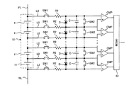
次に、電流遮断回路60の構成について、図5を用いて説明する。
Next, the configuration of the current interrupt
電流遮断回路60は、抵抗R2を有しており、抵抗R2は、各電圧検出ラインL2に設けられている。抵抗R2は、組電池10(単電池11)からの過電圧が電流遮断回路60に印加することを防止するために用いられる。すなわち、電流遮断回路60に過電圧が印加しようとするときには、抵抗R2が溶断することにより、電流遮断回路60に対する過電圧の印加を防止している。
The
電流遮断回路60は、複数のツェナーダイオードDを有する。各ツェナーダイオードDは、電圧検出ラインL2を介して、各単電池11と電気的に並列に接続されている。ここで、ツェナーダイオードDのカソードは、単電池11の正極端子と接続されており、ツェナーダイオードDのアノードは、単電池11の負極端子と接続されている。複数のツェナーダイオードDは、電気的に直列に接続されている。
The current interrupt
ツェナーダイオードDは、組電池10(単電池11)からの過電圧が電流遮断回路60に印加することを抑制するために用いられる。すなわち、電流遮断回路60に過電圧が印加しようとするときには、ツェナーダイオードDが導通状態となることにより、カソードからアノードの側に電流を流すことができる。これにより、後述するIC(Integrated Circuit)61の側に過電圧が印加されることを抑制することができる。
The Zener diode D is used for suppressing application of an overvoltage from the assembled battery 10 (unit cell 11) to the current interrupt
ツェナーダイオードDが導通状態となったとき、抵抗R2に電流を流すことにより、抵抗R2を溶断させることができる。すなわち、組電池10からIC61に過電圧が印加しようとしたときには、抵抗R2が溶断することにより、組電池10およびIC61の接続を遮断することができる。これにより、IC61を保護することができる。なお、電流遮断回路60への過電圧の印加を除外できれば、ツェナーダイオードDを省略することができる。
When the Zener diode D becomes conductive, the resistor R2 can be blown by passing a current through the resistor R2. That is, when an overvoltage is to be applied from the assembled
電流遮断回路60は、コンデンサCを有する。コンデンサCは、2つの電圧検出ラインL2を介して、単電池11と電気的に並列に接続されている。ここで、一方の電圧検出ラインL2に対するコンデンサCの接続点は、電圧検出ラインL2に対するツェナーダイオードD(カソード)の接続点と、コンパレータCMPとの間に位置している。
The current interrupt
また、他方の電圧検出ラインL2に対するコンデンサCの接続点は、電圧検出ラインL2に対するツェナーダイオードD(アノード)の接続点と、コントローラCMPとの間に位置している。複数の単電池11に対応して設けられた複数のコンデンサCは、電気的に直列に接続されている。
The connection point of the capacitor C to the other voltage detection line L2 is located between the connection point of the Zener diode D (anode) to the voltage detection line L2 and the controller CMP. The plurality of capacitors C provided corresponding to the plurality of
電流遮断回路60は、IC61を有する。IC61は、電池ECU30から起動信号を受けたり、停止信号を受けたりする。起動信号とは、電源からの電力をIC61に供給することを許容する信号であり、起動信号によって、IC61を動作させることができる。停止信号とは、電源からIC61への電力供給を停止させる信号であり、停止信号によって、IC61の動作を停止させることができる。
The
電池ECU30によってIC61の動作を停止させることができれば、図1に示す電池システムを停止させているときに、IC61の動作も停止させることができる。これにより、IC61の消費電力を低減することができる。
If the operation of the
IC61は、コンパレータCMPを有する。各単電池11の正極端子と接続された電圧検出ラインL2は、コンパレータCMPの負側入力端子と接続されている。また、各単電池11の負極端子と接続された電圧検出ラインL2は、コンパレータCMPの正側入力端子と接続されている。
The
ここで、図5に示すように、一方の単電池11の正極端子と、他方の単電池11の負極端子とに接続された電圧検出ラインL2は、分岐している。分岐された電圧検出ラインL2は、一方のコンパレータCMPにおける正側入力端子と、他方のコンパレータCMPにおける負側入力端子とにそれぞれ接続されている。
Here, as shown in FIG. 5, the voltage detection line L <b> 2 connected to the positive terminal of one
コンパレータCMPは、単電池11における正極端子および負極端子の電位差、言い換えれば、単電池11の電圧値を出力する。図5に示す構成では、コンパレータCMPがコンデンサCの電圧値を検出する。すなわち、図5に示す構成では、単電池11の電荷がコンデンサCにチャージされることにより、コンデンサCの電圧値は、単電池11の電圧値と等しくなる。そして、コンパレータCMPは、コンデンサCの電圧値(安定化された電圧値)を検出する。
The comparator CMP outputs the potential difference between the positive electrode terminal and the negative electrode terminal in the
IC61は、コンパレータCMPと接続されたOR回路62を有しており、コンパレータCMPの出力信号は、OR回路62に入力される。OR回路62は、複数のコンパレータCMPと接続されており、いずれかのコンパレータCMPの出力信号がOR回路62に入力されると、OR回路62は出力信号を生成する。
The
本実施例において、複数のコンパレータCMPは、互いに異なるタイミングで動作する。すなわち、複数のコンパレータCMPにおける出力信号は、互いに異なるタイミングにおいて、OR回路62に入力される。このため、各単電池11の電圧値が検出されるたびに、この電圧値に相当する信号をOR回路62が出力する。
In the present embodiment, the plurality of comparators CMP operate at different timings. That is, output signals from the plurality of comparators CMP are input to the
IC61は、OR回路62と接続されたアラーム確定回路(本発明のアラーム回路に相当する)63を有しており、OR回路62の出力信号は、アラーム確定回路63に入力される。アラーム確定回路63は、単電池11の過充電状態を判別し、単電池11が過充電状態であるときには、アラーム信号を出力する。アラーム信号とは、単電池11が過充電状態であることを示す信号である。
The
具体的には、図6に示すように、アラーム確定回路63は、コンパレータ63aによって構成することができる。OR回路62の出力信号(単電池11の電圧値Vb)は、コンパレータ63aにおける正側入力端子に入力される。また、閾値(電圧値)V_thは、コンパレータ63aにおける負側入力端子に入力される。
Specifically, as shown in FIG. 6, the
ここで、閾値(電圧値)V_thは、単電池11の過充電状態を判別するための電圧値であり、単電池11の充放電特性などを考慮して適宜設定することができる。例えば、閾値(電圧値)V_thとしては、単電池11が実際に過充電状態となるときの電圧値に設定したり、単電池11が実際に過充電状態となるときの電圧値よりも低い値に設定したりすることができる。ここで、閾値(電圧値)V_thは、図3に示すステップS102の処理で説明した上限電圧値Vc_thよりも高い値に設定することができる。
Here, the threshold value (voltage value) V_th is a voltage value for determining the overcharge state of the
OR回路62の出力信号(単電池11の電圧値Vb)が閾値(電圧値)V_thよりも高いときには、コンパレータ63aの出力信号(アラーム信号)が生成される。一方、OR回路62の出力信号(単電池11の電圧値Vb)が閾値(電圧値)V_thよりも低いときには、コンパレータ63aの出力信号(アラーム信号)が生成されない。
When the output signal of the OR circuit 62 (the voltage value Vb of the single battery 11) is higher than the threshold value (voltage value) V_th, the output signal (alarm signal) of the
一方、アラーム確定回路63としては、図7に示す構成を用いることもできる。図7において、コンパレータ63aの出力ラインには、コンデンサ63bの一端が接続されている。また、コンデンサ63bの他端は、接地されている。コンデンサ63bを設けることにより、アラーム確定回路63の出力信号にノイズが含まれてしまうことを抑制できる。すなわち、コンデンサ63bを用いてノイズを除去することにより、アラーム確定回路63の出力信号(アラーム信号)に対する信頼性を向上させることができる。
On the other hand, as the
図5において、IC61は、アラーム確定回路63と接続されたアラームラッチ回路64を有しており、アラーム確定回路63の出力信号(アラーム信号)が、アラームラッチ回路64に入力される。アラームラッチ回路64は、アラーム確定回路63からの入力信号を保持して、ラッチ信号(アラーム信号に相当する)を出力する。
In FIG. 5, the
IC61(アラームラッチ回路64)は、フォトカプラ65と接続されている。フォトカプラ65は、スイッチ素子として用いられ、アラームラッチ回路64からのラッチ信号を受けることにより、オフからオンに切り替わる。フォトカプラ65は、絶縁素子であるため、フォトカプラ65の入力側に位置する回路(高電圧回路)と、フォトカプラ65の出力側に位置する回路(低電圧回路)とを絶縁状態とすることができる。言い換えれば、フォトカプラ65は、入力信号としての高電圧信号を、出力信号としての低電圧信号に変更することができる。
The IC 61 (alarm latch circuit 64) is connected to the photocoupler 65. The photocoupler 65 is used as a switch element, and is switched from off to on by receiving a latch signal from the
フォトカプラ65は、OR回路66の入力端子と接続されている。フォトカプラ65がオフからオンに切り替わったときには、フォトカプラ65の出力信号が、OR回路66の入力端子に入力される。フォトカプラ65の出力信号がOR回路66に入力されれば、OR回路66の出力信号(アラーム信号に相当する)が生成される。
The photocoupler 65 is connected to the input terminal of the
本実施例では、アラームラッチ回路64およびOR回路66の間に、フォトカプラ65を設けているが、これに限るものではない。例えば、アラーム確定回路63およびアラームラッチ回路64の間に、フォトカプラ65を設けることもできる。
In this embodiment, the photocoupler 65 is provided between the
OR回路66の出力端子は、遅延回路67と接続されており、OR回路66の出力信号は、遅延回路67に入力される。遅延回路67は、OR回路66の出力信号が入力されてから所定時間が経過した後に、信号(アラーム信号に相当する)を出力する。遅延回路67は、トランジスタ(スイッチ)68と接続されている。トランジスタ68は、遅延回路67の出力信号を受けて、オンからオフに切り替わる。ここで、遅延回路67の出力信号がトランジスタ68に入力されていないとき、トランジスタ68は、オンになる。
The output terminal of the
トランジスタ68の一端は、電源69と接続されており、トランジスタ68の他端は、システムメインリレーSMR−B,SMR−Gの励磁コイル51と接続されている。図5に示す電源69は、図2に示す電源41と同じである。また、トランジスタ68は、図2に示すスイッチ42と同じである。このため、トランジスタ68は、上位ECU34からの制御信号を受けて動作したり、遅延回路67の出力信号を受けて動作したりする。
One end of the
図2を用いて説明したように、トランジスタ68がオンであるとき、電源69から励磁コイル51に電流が流れることにより、システムメインリレーSMR−B,SMR−Gがオンになる。一方、トランジスタ68がオフであるとき、電源69から励磁コイル51への電力供給が遮断され、システムメインリレーSMR−B,SMR−Gがオフになる。
As described with reference to FIG. 2, when the
本実施例によれば、IC61が単電池11の過充電状態を検出すると、IC61の出力信号(アラーム信号)がトランジスタ68に入力されることにより、システムメインリレーSMR−B,SMR−Gをオンからオフに切り替えることができる。これにより、過充電状態の単電池11に対して、充放電が行われることを防止できる。
According to this embodiment, when the
本実施例では、システムメインリレーSMR−B,SMR−G,SMR−Pが、上位ECU34からの制御信号を受けて、オンおよびオフの間で切り替わる。一方、単電池11が過充電状態となったときには、上位ECU34による制御ではなく、電流遮断回路60が、システムメインリレーSMR−B,SMR−Gをオンからオフに切り替える。このように、システムメインリレーSMR−B,SMR−Gの駆動制御は、上位ECU34を含む経路と、電流遮断回路60を含む経路とで別々に行われる。
In this embodiment, the system main relays SMR-B, SMR-G, and SMR-P are switched between on and off in response to a control signal from the
このため、上位ECU34や電池ECU30の設計を変更しても、この設計変更による影響を、電流遮断回路60は受けない。言い換えれば、上位ECU34や電池ECU30の設計を変更した後であっても、電流遮断回路60を使用し続けることができる。電流遮断回路60は、単電池11の過充電時にシステムメインリレーSMR−B,SMR−Gをオフにするための専用部品となり、汎用性を高めることができる。
For this reason, even if the design of the
上述したように、電流遮断回路60は、電子部品(主に、半導体素子)を用いて構成されており、コンピュータプログラムを用いた処理を行っていない。このため、電流遮断回路60を用いれば、プログラムのバグを考慮せずに、システムメインリレーSMR−B,SMR−Gを駆動することができる。また、通常、半導体素子では、摩耗劣化(経年劣化)が発生しにくいため、半導体素子を用いて電流遮断器60を構成することにより、部品(電流遮断回路60)の信頼性を向上させることができる。
As described above, the
なお、図5に示す構成では、組電池10に対して、1つの電流遮断回路60を設けているが、これに限るものではない。具体的には、組電池10を構成する、すべての単電池11を、複数のグループに分けたときには、各グループに対して電流遮断回路60を設けることができる。
In the configuration shown in FIG. 5, one current interrupt
ここで、グループ毎に電流遮断回路60を設ける場合には、フォトカプラ65の出力側に位置する回路を共用することができる。すなわち、図5に示す電流遮断回路60のうち、フォトカプラ65の入力側に位置する回路(フォトカプラ65を含む)を、グループの数だけ設けることができる。そして、各フォトカプラ65の出力信号を、OR回路66に入力させることができる。
Here, when the current cut-
本実施例において、OR回路66の入力端子は、電池ECU30と接続されており、電池ECU30の出力信号がOR回路66の入力端子に入力される。上述したように、電池ECU30は、IC61に対して、起動信号を出力したり、停止信号を出力したりする。このため、IC61を停止させる信号は、OR回路66にも入力される。
In this embodiment, the input terminal of the
フォトカプラ65の出力信号を受けたとき、又は、IC61の停止信号を電池ECU30から受けたとき、OR回路66は、出力信号を生成する。これにより、トランジスタ68をオンからオフに切り替えることができ、システムメインリレーSMR−B,SMR−Gをオンからオフに切り替えることができる。ここで、フォトカプラ65からOR回路66に信号が出力されていなく、かつ、IC61の停止信号が電池ECU30から出力されていないとき、OR回路66は、出力信号を生成しない。
When receiving the output signal of the photocoupler 65 or when receiving the stop signal of the
上述したように、IC61がアラーム信号を出力していなくても、電池ECU30がIC61の停止信号を出力したときには、トランジスタ68をオフにして、システムメインリレーSMR−B,SMR−Gをオフにすることができる。
As described above, even if the
これにより、IC61の動作を停止させるときには、組電池10およびインバータ22の接続を遮断して、組電池10の充放電を停止させることができる。言い換えれば、IC61の動作を停止させるときには、組電池10およびインバータ22が接続されたままとなることを防止できる。したがって、IC61が動作していない間に、組電池10の充放電が行われ、単電池11が過充電状態となってしまうことを防止できる。
Thereby, when stopping operation | movement of IC61, the connection of the assembled
一方、OR回路66の出力信号は、遅延回路67に入力されるだけでなく、電池ECU30にも入力される。すなわち、IC61からアラーム信号が出力されるときには、この情報が電池ECU30にも伝達される。これにより、電池ECU30は、単電池11の過充電状態によって、システムメインリレーSMR−B,SMR−Gがオンからオフに切り替わることを確認することができる。
On the other hand, the output signal of the
図1に示す電池システムを搭載した車両がエンジンを備えているとき、電池ECU30は、OR回路66の出力信号(アラーム信号)を受けることにより、エンジンを始動させることができる。具体的には、OR回路66の出力信号(アラーム信号)が電池ECU30に入力されたとき、電池ECU30は、OR回路66から取得した情報を上位ECU34に出力する。上位ECU34は、電池ECU30からの情報を受けて、エンジンを始動させる。ここで、組電池10の出力を用いて、エンジンを始動させることができる。
When the vehicle equipped with the battery system shown in FIG. 1 includes an engine, the
エンジンを既に始動しているときには、OR回路66の出力信号(アラーム信号)が電池ECU30に入力されている間、エンジンの始動を停止させないことができる。OR回路66の出力信号(アラーム信号)が発生しているときには、上述したように、システムメインリレーSMR−B,SMR−Gがオンからオフに切り替わり、組電池10の充放電が行われなくなる。この場合には、エンジンの始動を停止させないことにより、車両の走行を確保することができる。
When the engine is already started, the engine start can not be stopped while the output signal (alarm signal) of the
本実施例では、OR回路66およびトランジスタ68の間に、遅延回路67を設けている。このため、遅延回路67の出力に基づいて、システムメインリレーSMR−B,SMR−Gをオンからオフに切り替える前に、OR回路66の出力信号を電池ECU30に入力させて、エンジンを始動させることができる。すなわち、組電池10の充放電を停止させる前に、エンジンを始動させておくことができる。
In this embodiment, a
組電池10の出力電力を用いて、エンジンを始動させる構成では、エンジンを始動させる前に、組電池10の充放電を停止させてしまうと、組電池10の出力電力を用いてエンジンを始動させることができなくなってしまう。そこで、車両の走行を確保するためには、システムメインリレーSMR−B,SMR−Gをオンからオフに切り替える前に、エンジンを始動させておく必要がある。
In the configuration in which the engine is started using the output power of the assembled
本実施例では、遅延回路67を用いることにより、組電池10の出力電力によってエンジンを始動させる時間を確保した上で、システムメインリレーSMR−B,SMR−Gをオンからオフに切り替えることができる。これにより、組電池10の充放電を停止させる場合であっても、エンジンを用いて車両を走行させ続けることができる。
In this embodiment, by using the
なお、組電池10とは異なる電源(例えば、補機バッテリ)を用いてエンジンを始動させるときには、遅延回路67を省略することができる。エンジンを始動させるための電源として、組電池10以外の電源を用いれば、組電池10の充放電を停止させた後であっても、エンジンを始動させることができる。この場合には、システムメインリレーSMR−B,SMR−Gをオンからオフに切り替えるタイミングを遅延させる必要はなく、遅延回路67を省略することができる。
When starting the engine using a power source (for example, an auxiliary battery) different from the assembled
本実施例では、アラーム確定回路63からアラーム信号が出力されたときには、アラームラッチ回路64において、アラーム信号が保持される。すなわち、アラーム確定回路63からアラーム信号が出力された後では、アラームラッチ回路64から信号が出力され続け、システムメインリレーSMR−B,SMR−Gがオフのままとなる。アラームラッチ回路64を省略すると、単電池11の電圧値に応じて、アラーム確定回路63からアラーム信号が出力されたり、アラーム信号が出力されなかったりする。
In this embodiment, when an alarm signal is output from the
図8は、アラームラッチ回路64を省略した構成において、アラーム確定回路63の出力と、システムメインリレーSMR−B,SMR−Gのオン/オフとの関係を示す図である。
FIG. 8 is a diagram showing the relationship between the output of the
図8に示すように、単電池11の電圧値Vbが閾値V_thに到達することに応じて、アラーム確定回路63からアラーム信号が出力される。アラーム信号が出力されれば、システムメインリレーSMR−B,SMR−Gがオンからオフに切り替わる。これにより、組電池10(単電池11)の充放電が行われなくなり、組電池10(単電池11)の分極が解消される。
As shown in FIG. 8, an alarm signal is output from the
組電池10(単電池11)の充放電を行っているときには、組電池10に分極が発生し、単電池11の電圧値は、開放電圧に対して、分極に伴う電圧変化量の分だけ変化する。組電池10(単電池11)の充放電を停止させると、単電池11の分極が解消され、分極に相当する電圧変化量(電圧降下量)ΔVbだけ、単電池11の電圧値Vbが低下することになる。分極が解消すれば、電圧値Vbは、単電池11の開放電圧となる。
When charging / discharging the battery pack 10 (cell 11), polarization occurs in the
分極の解消に伴って、単電池11の電圧値Vbが低下すると、電圧値Vbが閾値V_thよりも低下することがある。特に、電圧変化量ΔVbが大きくなるほど、分極が解消した後の電圧値Vbは、閾値V_thよりも低下しやすくなる。
When the voltage value Vb of the
電圧変化量ΔVbは、単電池11に流れる電流値と、単電池11の内部抵抗との積で表される。このため、単電池11に流れる電流値(充電電流)が大きくなるほど、電圧変化量ΔVbが大きくなる。また、単電池11の内部抵抗が高くなるほど、電圧変化量ΔVbが大きくなる。ここで、単電池11の温度が低下するほど、単電池11の内部抵抗が上昇しやすくなる。
The voltage change amount ΔVb is represented by the product of the current value flowing through the
分極の解消に伴って、単電池11の電圧値Vbが閾値V_thよりも低くなると、アラーム確定回路63からは、アラーム信号が出力されず、トランジスタ68は、オフからオンに切り替わる。これにより、励磁コイル51への通電が許容され、システムメインリレーSMR−B,SMR−Gは、オフからオンに切り替わる。
When the voltage value Vb of the
システムメインリレーSMR−B,SMR−Gがオフからオンに切り替われば、組電池10(単電池11)の充放電が再開され、単電池11の電圧値Vbが再び閾値V_thよりも高くなってしまうことがある。電圧値Vbが閾値V_thよりも高くなれば、上述したように、電流遮断回路60によって、システムメインリレーSMR−B,SMR−Gがオンからオフに切り替わる。
When the system main relays SMR-B and SMR-G are switched from OFF to ON, charging / discharging of the assembled battery 10 (unit cell 11) is resumed, and the voltage value Vb of the
上述した電圧値Vbの挙動によれば、システムメインリレーSMR−B,SMR−Gがオンおよびオフの間で繰り返して切り替わることになってしまう。このように、システムメインリレーSMR−B,SMR−Gがオンおよびオフの間で繰り返して切り替わると、システムメインリレーSMR−B,SMR−Gの摩耗劣化が進行してしまう。 According to the behavior of the voltage value Vb described above, the system main relays SMR-B and SMR-G are repeatedly switched between on and off. As described above, when the system main relays SMR-B and SMR-G are repeatedly switched between ON and OFF, wear deterioration of the system main relays SMR-B and SMR-G proceeds.
本実施例では、アラームラッチ回路64を設けているため、アラーム確定回路63からアラーム信号が出力されたときには、図9に示すように、アラームラッチ回路64によってアラーム信号が保持される。アラーム信号が保持されれば、システムメインリレーSMR−B,SMR−Gは、オフのままとなる。
In this embodiment, since the
これにより、図8に示す電圧値Vbの挙動によって、システムメインリレーSMR−B,SMR−Gがオンおよびオフの間で繰り返して切り替わることを防止できる。ここで、システムメインリレーSMR−B,SMR−Gは、オフのままであるため、単電池11の電圧値Vbは、電圧変化量ΔVbだけ低下した状態に維持される。言い換えれば、単電池11の電圧値Vbは、開放電圧に維持される。
Accordingly, it is possible to prevent the system main relays SMR-B and SMR-G from repeatedly switching between on and off by the behavior of the voltage value Vb shown in FIG. Here, since system main relays SMR-B and SMR-G remain off, voltage value Vb of
次に、電流遮断回路60の異常状態を判別する構成について、図10を用いて説明する。図10は、電流遮断回路60の一部の構成を示す図であり、電流遮断回路60の異常状態を判別するために、図5に示す構成に対して、後述するスイッチSW1,SW2を追加している。ここで、異常状態とは、電流遮断回路60が正常に動作していない状態をいう。
Next, a configuration for determining an abnormal state of the current interrupt
各電圧検出ラインL2には、スイッチ(本発明の第2スイッチに相当する)SW1が設けられている。具体的には、スイッチSW1は、単電池11の電極端子(正極端子又は負極端子)および抵抗R2の間に設けられている。ここで、複数のスイッチSW1は、マルチプレクサによって構成することができる。各スイッチSW1は、電池ECU30からの制御信号を受けることにより、オンおよびオフの間で切り替わる。
Each voltage detection line L2 is provided with a switch (corresponding to a second switch of the present invention) SW1. Specifically, the switch SW1 is provided between the electrode terminal (positive electrode terminal or negative electrode terminal) of the
スイッチ(本発明の第1スイッチに相当する)SW2は、2つの電圧検出ラインL2を介して、単電池11と電気的に並列に接続されている。すなわち、スイッチSW2は、コンデンサCと電気的に並列に接続されたバイパス回路に設けられている。スイッチSW2は、電池ECU30からの制御信号を受けることにより、オンおよびオフの間で切り替わる。
The switch (corresponding to the first switch of the present invention) SW2 is electrically connected in parallel with the
一方の電圧検出ラインL2に対するスイッチSW2の接続点は、一方の電圧検出ラインL2に対するコンデンサCの接続点と、コンパレータCMPとの間に位置している。また、他方の電圧検出ラインL2に対するスイッチSW2の接続点は、他方の電圧検出ラインL2に対するコンデンサCの接続点と、コンパレータCMPとの間に位置している。 The connection point of the switch SW2 with respect to one voltage detection line L2 is located between the connection point of the capacitor C with respect to one voltage detection line L2 and the comparator CMP. The connection point of the switch SW2 with respect to the other voltage detection line L2 is located between the connection point of the capacitor C with respect to the other voltage detection line L2 and the comparator CMP.
図11に示すように、電池ECU30が、スイッチSW1a,SW1c,SW2aだけをオフからオンに切り替えると、単電池11Bに対応したコンデンサCbには、図11の点線で示す経路に沿って、単電池11A,11Bの電荷がチャージされる。すなわち、コンデンサCbの電圧値は、単電池11A,11Bの端子間電圧と等しくなる。これにより、コンパレータCMPbは、コンデンサCbの電圧値を出力する。
As shown in FIG. 11, when the
図6又は図7を用いて説明したように、アラーム確定回路63は、コンデンサCbの電圧値と、閾値(電圧値)V_thとを比較する。ここで、コンデンサCbの電圧値は、図11に示す単電池11Bの電圧値ではなく、単電池11A,11Bの電圧値であるため、閾値(電圧値)V_thよりも高くなりやすい。コンデンサCbの電圧値が、閾値(電圧値)V_thよりも高いと、アラーム確定回路63は、単電池11が過充電状態であることを示すアラーム信号を出力する。このアラーム信号は、電流遮断回路60の異常状態を判別するために用いられる。
As described with reference to FIG. 6 or FIG. 7, the
アラーム確定回路63がアラーム信号を出力すれば、上述したように、システムメインリレーSMR−B,SMR−Gがオンからオフに切り替わり、組電池10の充放電が停止する。組電池10の充放電が停止すれば、インバータ22に入力される電圧値が0[V]となったり、組電池10に流れる電流値が0[A]となったりする。
When the
図11に示す例では、コンデンサCbの電圧値を、2つの単電池11A,11Bの電圧値としているが、これに限るものではない。すなわち、電気的に直列に接続された3つ以上の単電池11の電荷を、1つのコンデンサCにチャージすることにより、コンデンサCの電圧値を、3つ以上の単電池11の電圧値とすることができる。3つ以上の単電池11の電荷を、1つのコンデンサCにチャージするときでも、図11に示す場合と同様に、スイッチSW1,SW2のオン/オフを制御すればよい。
In the example shown in FIG. 11, the voltage value of the capacitor Cb is the voltage value of the two
ここで、コンデンサCに電荷をチャージする単電池11の数は、コンデンサCの耐電圧を考慮して適宜設定することができる。すなわち、コンデンサCに電荷をチャージする複数の単電池11の電圧値が、コンデンサCの耐電圧を超えないように、単電池11の数を設定することができる。
Here, the number of the
また、組電池10を放電した後では、単電池11の電圧値が低下しているため、電池ECU30によって検出された単電池11の電圧値に基づいて、コンデンサCに電荷をチャージする単電池11の数を設定することができる。具体的には、単電池11の電圧値が低下しているほど、1つのコンデンサCに電荷をチャージする単電池11の数を増やすことができる。これにより、アラーム確定回路63に入力される電圧値を、閾値(電圧値)V_thよりも高くすることができ、アラーム確定回路63からアラーム信号を出力させることができる。
Further, since the voltage value of the
次に、電流遮断回路60の異常状態を判別する処理について、図12に示すフローチャートを用いて説明する。図12に示す処理は、電池ECU30によって実行される。
Next, processing for determining an abnormal state of the current interrupt
ステップS201において、電池ECU30は、図10に示す複数のスイッチSW1,SW2におけるオン/オフを制御する。例えば、図11に示すように、2つの単電池11A,11Bの電荷をコンデンサCbにチャージするとき、電池ECU30は、スイッチSW1a,SW1c,SW2aだけをオフからオンに切り替える。ここで、スイッチSW1a,SW1c,SW2a以外の他のスイッチSW1,SW2については、オフのままにしておく。
In step S201, the
ステップS201の処理を行うと、図11を用いて説明したように、コンデンサCbの電圧値が単電池11A,11Bの電圧値と等しくなり、アラーム確定回路63で比較される閾値(電圧値)V_thよりも高くなる。これにより、アラーム確定回路63は、アラーム信号を出力し、システムメインリレーSMR−B,SMR−Gをオンからオフに切り替える。これに伴って、組電池10の充放電が停止する。
When the processing of step S201 is performed, as described with reference to FIG. 11, the voltage value of the capacitor Cb becomes equal to the voltage value of the
ステップS202において、電池ECU30は、電圧センサ24を用いて、インバータ22に入力される電圧値VLを検出する。そして、電池ECU30は、電圧値VLが閾値(電圧値)Vminよりも高いか否かを判別する。閾値Vminは、組電池10の充放電が停止しているか否かを判別するための値であり、閾値Vminに関する情報は、メモリに記憶することができる。
In step S <b> 202, the
ステップS201の処理によって、組電池10の充放電が停止しているため、インバータ22に入力される電圧値は、0[V]となる。このため、閾値Vminとしては、例えば、0[V]に設定することができる。なお、電圧センサ24の検出誤差を考慮して、閾値Vminを、0[V]よりも高い値に設定することもできる。
Since charging / discharging of the assembled
ステップS202において、電圧値VLが閾値Vminよりも高いとき、電池ECU30は、ステップS203の処理を行う。一方、電圧値VLが閾値Vminよりも低いとき、電池ECU30は、ステップS204の処理を行う。
In step S202, when the voltage value VL is higher than the threshold value Vmin, the
ステップS203において、電池ECU30は、電流遮断回路60が異常状態であることを判別する。電流遮断回路60が正常に動作していれば、上述したように、アラーム確定回路63からアラーム信号が出力され、組電池10の充放電が停止することになる。
In step S203, the
一方、電流遮断回路60が異常状態であれば、アラーム確定回路63からアラーム信号が出力されなかったり、アラームラッチ回路64の出力信号がトランジスタ68に入力されなかったりすることがある。この場合には、システムメインリレーSMR−B,SMR−Gがオンからオフに切り替わらず、組電池10の充放電が継続されることになる。
On the other hand, if the current interrupt
組電池10の充放電が継続されていれば、電圧値VLが閾値Vminよりも高くなる。この場合において、電池ECU30は、意図的にアラーム信号を出力させる制御を行っているにも関わらず、組電池10の充放電が停止していないことを確認することができる。これにより、電池ECU30は、電流遮断回路60が異常状態であることを判別することができる。
If charging / discharging of the assembled
ステップS204において、電池ECU30は、電流遮断回路60が正常状態であることを判別する。電圧値VLが閾値Vminよりも低いときには、組電池10の充放電が停止していることになるため、電池ECU30は、電流遮断回路60が正常に動作していることを判別することができる。すなわち、電池ECU30は、意図的に生成したアラーム信号によって、システムメインリレーSMR−B,SMR−Gがオンからオフに切り替わっていることを確認することができる。
In step S204, the
図12に示す処理では、電圧センサ24の出力に基づいて、電流遮断回路60の異常状態を判別しているが、これに限るものではない。上述したように、電流遮断回路60から出力されたアラーム信号によって、システムメインリレーSMR−B,SMR−Gがオンからオフに切り替わったときには、組電池10に電流が流れないことになる。このため、電流センサ21の出力に基づいて、電流遮断回路60の異常状態を判別することもできる。
In the process illustrated in FIG. 12, the abnormal state of the current interrupt
具体的には、図13に示す処理を行うことにより、電流遮断回路60の異常状態を判別することができる。図13において、図12で説明した処理と同じ処理については、同一の符号を用いている。図13に示す処理では、図12に示すステップS202の処理の代わりに、ステップS205の処理を行っている。
Specifically, the abnormal state of the current interrupt
ステップS205において、電池ECU30は、電流センサ21を用いて、組電池10に流れる電流値Ibを検出する。そして、電池ECU30は、電流値Ibが閾値Iminよりも大きいか否かを判別する。閾値Iminは、組電池10の充放電が停止しているか否かを判別するための値であり、閾値Iminに関する情報は、メモリに記憶することができる。
In step S <b> 205, the
ステップS201の処理によって、組電池10の充放電が停止しているため、組電池10には電流が流れないことになる。このため、閾値Iminとしては、例えば、0[A]に設定することができる。なお、電流センサ21の検出誤差を考慮して、閾値Iminを、0[A]とは異なる値に設定することもできる。
Since charging / discharging of the assembled
上述したように、組電池10を放電しているときには、電流センサ21によって検出される電流値Ibが正の値となり、組電池10を充電しているときには、電流センサ21によって検出される電流値Ibが負の値となる。このため、ステップS205の処理において、電流値Ibおよび閾値Iminを比較するときには、これらの絶対値を比較することが好ましい。
As described above, when the
ステップS205において、電流値Ibが閾値Iminよりも大きいとき、電池ECU30は、ステップS203の処理を行う。一方、電流値Ibが閾値Iminよりも小さいとき、電池ECU30は、ステップS204の処理を行う。
In step S205, when the current value Ib is larger than the threshold value Imin, the
本実施例では、図10に示すスイッチSW1,SW2のオン/オフを制御することにより、アラーム確定回路63において、過充電の判別を行わせているが、これに限るものではない。具体的には、図6又は図7に示すアラーム確定回路63において、コンパレータ63aに入力される基準電圧(閾値V_th)を変更することにより、アラーム確定回路63において、過充電の判別を行わせることができる。
In this embodiment, overcharge is determined in the
具体的には、図14に示すように、コンパレータ63aの負側入力端子には、スイッチ63cが接続されており、スイッチ63cを切り替えることにより、コンパレータ63aに入力される基準電圧を変更することができる。具体的には、基準電圧としての閾値V_th1又は閾値V_th2をコンパレータ63aに入力することができる。
Specifically, as shown in FIG. 14, a
電池ECU30は、スイッチ63cの駆動を制御することができる。閾値V_th1は、単電池11の過充電状態を判別するために用いられる。すなわち、閾値V_th1は、図6又は図7に示す閾値V_thと同じである。組電池10を充放電している間に、電流遮断回路60によって単電池11の過充電状態を判別するときには、電池ECU30は、スイッチ63cの駆動を制御して、閾値V_th1をコンパレータ63aに入力させる。
The
一方、閾値V_th2は、電流遮断回路60の異常状態を判別するために用いられる。そして、閾値V_th2は、閾値V_th1よりも低い値である。電流遮断回路60の異常状態を判別するとき、電池ECU30は、スイッチ63cの駆動を制御することにより、閾値V_th2をコンパレータ63aに入力させる。
On the other hand, the threshold value V_th2 is used to determine an abnormal state of the current interrupt
閾値V_th2は、閾値V_th1よりも低いため、コンパレータ63aに入力される単電池11の電圧値Vbは、閾値V_th2よりも高くなりやすい。このため、閾値V_th2がコンパレータ63aに入力されているときには、アラーム確定回路63からアラーム信号が出力される。このアラーム信号によって、システムメインリレーSMR−B,SMR−Gをオンからオフに切り替えることができ、図12又は図13に示す処理によって、電流遮断回路60が異常状態であるか否かを判別することができる。
Since the threshold value V_th2 is lower than the threshold value V_th1, the voltage value Vb of the
図14に示す構成では、コンパレータ63aに入力される基準電圧を変更しているが、これに限るものではない。具体的には、図15に示すように、コンパレータ63aの負側入力端子に入力される基準電圧(閾値V_th)は変更せずに、コンパレータ63aの正側入力端子に入力される電圧値を変更することができる。
In the configuration shown in FIG. 14, the reference voltage input to the
図15に示す構成において、コンパレータ63aの正側入力端子には、スイッチ63dが接続されている。スイッチ63dは、電池ECU30からの制御信号を受けて動作する。スイッチ63dは、単電池11の電圧値Vbをコンパレータ63aに入力させたり、電源からの電圧値Vcをコンパレータ63aに入力させたりする。電源としては、例えば、安定化電源を用いることができる。
In the configuration shown in FIG. 15, a
電圧値Vcは、閾値V_thよりも高い値であり、適宜設定することができる。電圧値Vcをコンパレータ63aに入力したときには、電圧値Vcが閾値V_thよりも高くなるため、アラーム確定回路63は、アラーム信号を出力する。したがって、電流遮断回路60の異常状態を判別するとき、電池ECU30は、スイッチ63dの駆動を制御することにより、電圧値Vcをコンパレータ63aに入力させることができる。そして、図12又は図13に示す処理によって、電流遮断回路60が異常状態であるか否かを判別することができる。
The voltage value Vc is higher than the threshold value V_th and can be set as appropriate. When the voltage value Vc is input to the
なお、組電池10の充放電を行っている間に、電流遮断回路60によって単電池11の過充電状態を判別するときには、電池ECU30は、スイッチ63dの駆動を制御することにより、単電池11の電圧値Vbをコンパレータ63aに入力させることができる。これにより、単電池11が過充電状態であるときには、電流遮断回路60から出力されたアラーム信号によって、システムメインリレーSMR−B,SMR−Gをオンからオフに切り替えることができる。
Note that when the overcurrent state of the
本実施例によれば、単電池11が過充電状態ではなくても、電池ECU30から出力された指令に基づいて、電流遮断回路60において、単電池11が過充電状態であることを判別させることができる。言い換えれば、単電池11が過充電状態ではなくても、電流遮断回路60からアラーム信号を出力させることができる。これにより、電流遮断回路60からアラーム信号が正常に出力されるか否かを確認することができ、電流遮断回路60が異常状態であるか否かを判別することができる。
According to the present embodiment, even if the
本発明の実施例2について説明する。本実施例において、実施例1で説明した構成要素と同じ構成要素については、同一の符号を用い、詳細な説明は省略する。以下、実施例1と異なる点について、主に説明する。 A second embodiment of the present invention will be described. In the present embodiment, the same components as those described in the first embodiment are denoted by the same reference numerals, and detailed description thereof is omitted. Hereinafter, differences from the first embodiment will be mainly described.
実施例1では、アラーム確定回路63において、過充電の判別を行わせることにより、アラーム信号を出力させて、システムメインリレーSMR−B,SMR−Gをオンからオフに切り替えている。本実施例では、アラーム確定回路63において、過放電の判別を行わせることにより、アラーム信号を出力させて、システムメインリレーSMR−B,SMR−Gをオンからオフに切り替えるようにしている。
In the first embodiment, the
図16は、本実施例における電池ECU30の一部の構成を示す図である。図16に示すように、電圧検出ラインL1,L2の一部は、共用されており、電圧検出ラインL1には、図5に示す抵抗R2、ツェナーダイオードDおよびコンデンサCが接続されている。ここで、図16に示すように、電圧検出ラインL1,L2の分岐部分は、コンデンサCおよび監視IC31の間に位置している。
FIG. 16 is a diagram illustrating a partial configuration of the
一方、図16に示す構成では、図5に示す構成に加えて、各電圧検出ラインL1,L2に抵抗R3が設けられている。具体的には、抵抗R3は、電圧検出ラインL1,L2に対するダイオードDの接続点と、電圧検出ラインL1,L2に対するコンデンサCの接続点との間に設けられている。 On the other hand, in the configuration shown in FIG. 16, in addition to the configuration shown in FIG. 5, resistors R3 are provided in the voltage detection lines L1 and L2. Specifically, the resistor R3 is provided between a connection point of the diode D to the voltage detection lines L1 and L2 and a connection point of the capacitor C to the voltage detection lines L1 and L2.
抵抗R2,R3は、電気的に直列に接続されている。抵抗R3の抵抗値は、抵抗R2の抵抗値よりも大きくなっており、抵抗R3は、複数の単電池11における電圧値を均等化させるために用いられる。複数の単電池11における電圧値を均等化させることを、均等化処理という。
The resistors R2 and R3 are electrically connected in series. The resistance value of the resistor R3 is larger than the resistance value of the resistor R2, and the resistor R3 is used to equalize voltage values in the plurality of
組電池10を構成する複数の単電池11では、自己放電特性や内部抵抗のバラツキが発生することがあり、このバラツキに伴って、複数の単電池11における電圧値にバラツキが発生する。複数の単電池11において、電圧値のバラツキが発生していると、すべての単電池11を効率良く充放電させることができなくなってしまう。そこで、複数の単電池11における電圧値を揃えることが好ましい。ここで、均等化処理を行えば、複数の単電池11における電圧値のバラツキを抑制することができる。
In the plurality of
例えば、特定の単電池11の電圧値が、他の単電池11の電圧値よりも高いときには、均等化処理を行うことにより、特定の単電池11だけを放電させることができる。ここで、抵抗R3には、単電池11の放電電流を流すことができる。特定の単電池11だけを放電させれば、特定の単電池11の電圧値を、他の単電池11の電圧値に揃えることができる。
For example, when the voltage value of a
監視IC31は、複数のスイッチSW3を有しており、スイッチSW3は、単電池11の数だけ設けられている。スイッチSW3は、単電池11の電極端子(正極端子や負極端子)と接続された2つの電圧検出ラインL1に接続されている。また、スイッチSW3は、コンデンサCと電気的に並列に接続されたバイパス回路に設けられている。スイッチSW3は、CPU33(図1参照)からの制御信号を受けて、オンおよびオフの間で切り替わる。
The
スイッチSW3は、上述した均等化処理を行うために用いられる。すなわち、特定のスイッチSW3をオンにすれば、特定のスイッチSW3に対応した単電池11だけを放電させることができる。このときの放電電流は、抵抗R2,R3およびスイッチSW3を流れる。これにより、上述したように、複数の単電池11における電圧値のバラツキを抑制することができる。
The switch SW3 is used for performing the equalization process described above. That is, if the specific switch SW3 is turned on, only the
監視IC31は、コンパレータ31aを有している。コンパレータ31aの2つの入力端子は、電圧検出ラインL1を介して、単電池11の正極端子および負極端子とそれぞれ接続されている。これにより、コンパレータ31aは、単電池11の電圧値を検出することができる。図16に示す構成では、単電池11の電荷がコンデンサCにチャージされることにより、コンデンサCの電圧値が単電池11の電圧値と等しくなる。そして、コンパレータ31aは、コンデンサCの電圧値を検出する。コンパレータ31aの出力信号は、フォトカプラ32(図1参照)に入力される。
The
一方、本実施例におけるアラーム確定回路63としては、図17に示す構成を用いることができる。図17に示すように、アラーム確定回路63は、第1コンパレータ63eおよび第2コンパレータ63fを有する。第1コンパレータ63eは、単電池11の過充電状態を判別するために用いられる。すなわち、第1コンパレータ63eは、実施例1で説明した図6又は図7に示すコンパレータ63aと同じである。
On the other hand, the configuration shown in FIG. 17 can be used as the
第1コンパレータ63eには、OR回路62の出力(単電池11の電圧値Vb)と、基準電圧としての閾値Vu_thとが入力される。閾値Vu_thは、単電池11の過充電状態を判別するための値であり、実施例1で説明した閾値V_th(図6又は図7参照)と同じである。単電池11の電圧値Vbが閾値Vu_thよりも高いとき、第1コンパレータ63eは、単電池11が過充電状態であることを示すアラーム信号を出力する。一方、単電池11の電圧値Vbが閾値Vu_thよりも低いとき、第1コンパレータ63eは、アラーム信号を出力しない。
The output of the OR circuit 62 (the voltage value Vb of the unit cell 11) and the threshold value Vu_th as the reference voltage are input to the
第2コンパレータ63fは、単電池11の過放電状態を判別するために用いられる。ここで、第2コンパレータ63fには、OR回路62の出力(単電池11の電圧値Vb)と、基準電圧としての閾値Vl_thとが入力される。閾値Vl_thは、単電池11の過放電状態を判別するための値であり、適宜設定することができる。単電池11の電圧値Vbが閾値Vl_thよりも低いとき、第2コンパレータ63eは、単電池11が過放電状態であることを示すアラーム信号を出力する。一方、単電池11の電圧値Vbが閾値Vl_thよりも高いとき、第2コンパレータ63eは、アラーム信号を出力しない。
The
アラームラッチ回路64は、第1コンパレータ63e又は第2コンパレータ63fから出力されたアラーム信号を保持する。上述したように、本実施例では、単電池11が過充電状態又は過放電状態であるときに、電流遮断回路60からアラーム信号が出力されるようになっている。そして、アラーム信号に基づいて、システムメインリレーSMR−B,SMR−Gをオンからオフに切り替えることができる。
The
図16に示す構成において、均等化処理を行うために、スイッチSW3をオンにすると、単電池11の放電電流は、スイッチSW3に流れ、コンデンサCには流れにくくなる。このため、コンデンサCの電圧値は、単電池11の電圧値よりも低くなる。電流遮断回路60のコンパレータCMPは、図5を用いて説明したように、コンデンサCの電圧値を検出する。コンパレータCMPから出力される電圧値は、単電池11の電圧値よりも低いため、アラーム確定回路63で比較される閾値Vl_th(図17参照)よりも低くなりやすい。
In the configuration shown in FIG. 16, when the switch SW3 is turned on to perform the equalization process, the discharge current of the
コンパレータCMPから出力される電圧値が閾値Vl_thよりも低いと、上述したように、アラーム確定回路63(コンパレータ63f)からアラーム信号が出力される。このアラーム信号に基づいて、システムメインリレーSMR−B,SMR−Gをオンからオフに切り替えて、組電池10の充放電を停止させることができる。
When the voltage value output from the comparator CMP is lower than the threshold value Vl_th, an alarm signal is output from the alarm confirmation circuit 63 (
なお、単電池11が過充電状態に到達したときには、コンパレータCMPから出力される電圧値が閾値Vu_thよりも高くなり、アラーム確定回路63(コンパレータ63e)からアラーム信号が出力される。このアラーム信号に基づいて、システムメインリレーSMR−B,SMR−Gをオンからオフに切り替えて、組電池10の充放電を停止させることができる。
When the
次に、電流遮断回路60の異常状態を判別する処理について、図18に示すフローチャートを用いて説明する。図18に示す処理は、電池ECU30によって実行される。ここで、図18に示す処理のうち、図12で説明した処理と同じ処理については、同一の符号を用いており、詳細な説明は省略する。
Next, processing for determining an abnormal state of the current interrupt
図18に示す処理では、図12に示すステップS201の処理の代わりに、ステップS301の処理を行っている。ステップS301において、電池ECU30は、均等化処理に用いられるスイッチSW3をオフからオンに切り替える。
In the process shown in FIG. 18, the process of step S301 is performed instead of the process of step S201 shown in FIG. In step S301, the
ステップS301の処理では、すべてのスイッチSW3をオフからオンに切り替えることができる。これにより、図16に示す、すべてのコンデンサCに電流が流れにくくなり、各コンデンサCの電圧値を、各単電池11の電圧値よりも低くすることができる。これにより、図5に示す、すべてのコンパレータCMPから出力される電圧値は、閾値Vu_thよりも低くなり、アラーム確定回路63(コンパレータ63f)からは、アラーム信号が出力される。
In the process of step S301, all the switches SW3 can be switched from off to on. Accordingly, it becomes difficult for current to flow through all the capacitors C shown in FIG. 16, and the voltage value of each capacitor C can be made lower than the voltage value of each
アラーム信号が出力されれば、組電池10の充放電が停止することになるため、ステップS202の処理を行うことにより、電流遮断回路60が異常状態であるか否かを判別することができる。
If the alarm signal is output, charging / discharging of the assembled
すなわち、電圧センサ24によって検出された電圧値VLが閾値Vminよりも低ければ、アラーム確定回路63からアラーム信号が出力されており、電池ECU30は、電流遮断回路60が正常に動作していることを判別することができる。また、電圧値VLが閾値Vminよりも高ければ、アラーム確定回路63からアラーム信号が出力されていなく、電池ECU30は、電流遮断回路60が異常状態であることを判別することができる。
That is, if the voltage value VL detected by the
なお、図18に示すステップS202の処理では、電圧センサ24の電圧値VLを閾値Vminと比較しているが、これに限るものではない。具体的には、図13を用いて説明したように、電流センサ21によって検出された電流値Ibを閾値Iminと比較することもできる。
In the process of step S202 shown in FIG. 18, the voltage value VL of the
本実施例によれば、単電池11が過放電状態ではなくても、電池ECU30から出力された指令に基づいて、電流遮断回路60において、単電池11が過放電状態であることを判別させることができる。言い換えれば、単電池11が過放電状態ではなくても、電流遮断回路60からアラーム信号を出力させることができる。これにより、電流遮断回路60からアラーム信号が正常に出力されているか否かを確認することができ、電流遮断回路60が異常状態であるか否かを判別することができる。
According to the present embodiment, even if the
10:組電池(蓄電装置)、11:単電池(蓄電素子)、21:電流センサ、
22:インバータ、23:モータ・ジェネレータ、24:電圧センサ、
30:電池ECU(コントローラ)、31:監視IC、32:フォトカプラ、
33:CPU、34:上位ECU(コントローラ)、41:電源、42:スイッチ、
51:励磁コイル、52:可動接点、53:固定接点、60:電流遮断回路、
61:IC、62:OR回路、63:アラーム確定回路(アラーム回路)、
63a:コンパレータ、63b:コンデンサ、64:アラームラッチ回路、
65:フォトカプラ、66:OR回路、67:遅延回路、68:トランジスタ、
69:電源
10: assembled battery (power storage device), 11: single battery (power storage element), 21: current sensor,
22: Inverter, 23: Motor generator, 24: Voltage sensor,
30: Battery ECU (controller), 31: Monitoring IC, 32: Photocoupler,
33: CPU, 34: host ECU (controller), 41: power supply, 42: switch,
51: Excitation coil, 52: Movable contact, 53: Fixed contact, 60: Current interruption circuit,
61: IC, 62: OR circuit, 63: Alarm confirmation circuit (alarm circuit),
63a: comparator, 63b: capacitor, 64: alarm latch circuit,
65: Photocoupler, 66: OR circuit, 67: Delay circuit, 68: Transistor,
69: Power supply
Claims (7)
前記各蓄電ブロックと並列に接続され、前記各蓄電ブロックの電圧値を出力するコンデンサと、
前記蓄電装置および負荷を接続するオンと、前記蓄電装置および前記負荷の接続を遮断するオフとの間で切り替わるリレーと、
前記リレーの前記オンおよび前記オフを制御するコントローラと、
前記リレーを前記オンから前記オフに切り替えて、前記蓄電装置の通電を遮断する電流遮断回路と、を有し、
前記電流遮断回路は、
前記コンデンサから入力される前記各蓄電ブロックの電圧値および閾値を比較して、前記各蓄電ブロックが過充電状態であることを示すアラーム信号を出力するアラーム回路と、
前記アラーム信号を保持するラッチ回路と、
前記ラッチ回路の出力信号を受けて、前記リレーを前記オンから前記オフに切り替えるトランジスタと、を有しており、
前記コントローラは、複数の前記蓄電ブロックの出力を用いて1つの前記コンデンサを充電することにより、前記アラーム回路から、過充電状態を示す前記アラーム信号を出力させる制御を行った後に、前記蓄電装置の通電状態を判別することを特徴とする蓄電システム。 A power storage device in which a plurality of power storage blocks each including a power storage element that performs charging and discharging are connected in series,
A capacitor connected in parallel with each of the storage blocks and outputting a voltage value of each of the storage blocks;
A relay that switches between on to connect the power storage device and the load and off to cut off the connection of the power storage device and the load;
A controller for controlling the on and off of the relay;
A current cut-off circuit that switches the relay from the on to the off and cuts off the energization of the power storage device,
The current interrupt circuit is
By comparing the voltage value and the threshold of the respective storage block input from the capacitor, and an alarm circuit for outputting an alarm signal indicating that said respective storage blocks is overcharged state,
A latch circuit for holding the alarm signal;
A transistor that receives the output signal of the latch circuit and switches the relay from the on to the off;
The controller performs control to output the alarm signal indicating an overcharge state from the alarm circuit by charging one of the capacitors using outputs of the plurality of power storage blocks, and then An electricity storage system characterized by determining an energized state.
前記各蓄電ブロックおよび前記各コンデンサを接続する第2スイッチと、を有し、
前記コントローラは、前記第1スイッチおよび前記第2スイッチを駆動して、複数の前記蓄電ブロックの出力を用いて1つの前記コンデンサを充電することを特徴とする請求項1に記載の蓄電システム。 Is connected in parallel with the previous SL each capacitor, a bypass circuit including a first switch,
A second switch for connecting each power storage block and each capacitor;
Wherein the controller, the power storage system according to claim 1 wherein first driving switch and the second switch, characterized by the Turkey to charge one of the capacitors using the output of a plurality of said power storage block .
前記蓄電装置および負荷を接続するオンと、前記蓄電装置および前記負荷の接続を遮断するオフとの間で切り替わるリレーと、
前記リレーの前記オンおよび前記オフを制御するコントローラと、
前記リレーを前記オンから前記オフに切り替えて、前記蓄電装置の通電を遮断する電流遮断回路と、
前記蓄電ブロックおよび前記電流遮断回路を接続するラインから分岐したラインを用いて、前記各蓄電ブロックと並列に接続されており、スイッチの動作によって前記各蓄電ブロックを放電させる放電回路と、を有し、
前記電流遮断回路は、
入力される前記各蓄電ブロックの電圧値および閾値を比較して、前記各蓄電ブロックが過放電状態であることを示すアラーム信号を出力するアラーム回路と、
前記アラーム信号を保持するラッチ回路と、
前記ラッチ回路の出力信号を受けて、前記リレーを前記オンから前記オフに切り替えるトランジスタと、を有しており、
前記コントローラは、前記放電回路の前記スイッチの駆動によって、前記蓄電ブロックから前記放電回路への放電を許容して、前記アラーム回路に入力される電圧値を低下させることにより、過放電状態を示す前記アラーム信号を出力させる制御を行った後に、前記蓄電装置の通電状態を判別することを特徴とする蓄電システム。 A power storage device in which a plurality of power storage blocks each including a power storage element that performs charging and discharging are connected in series,
A relay that switches between on to connect the power storage device and the load and off to cut off the connection of the power storage device and the load;
A controller for controlling the on and off of the relay;
A current interruption circuit that switches the relay from the on to the off and cuts off the energization of the power storage device;
Using a line branched from said power storage block and line connecting the current cutoff circuit, the connected in parallel with the respective storage block has a discharge circuit for discharging the respective storage blocks by operation of the switch ,
The current interrupt circuit is
An alarm circuit that compares the input voltage value and threshold value of each power storage block and outputs an alarm signal indicating that each power storage block is in an overdischarge state;
A latch circuit for holding the alarm signal;
A transistor that receives the output signal of the latch circuit and switches the relay from the on to the off;
The controller allows the discharge from the power storage block to the discharge circuit by driving the switch of the discharge circuit, and reduces the voltage value input to the alarm circuit, thereby indicating the overdischarge state. power storage system, wherein a control to output an alarm signal after Tsu line, to determine the current state of the power storage device.
前記放電回路は、前記コンデンサと並列に接続されていることを特徴とする請求項3に記載の蓄電システム。 A capacitor that is connected in parallel with each power storage block and outputs a voltage value of each power storage block to the alarm circuit;
The power storage system according to claim 3 , wherein the discharge circuit is connected in parallel with the capacitor.
Priority Applications (5)
| Application Number | Priority Date | Filing Date | Title |
|---|---|---|---|
| JP2012264010A JP5708625B2 (en) | 2012-12-03 | 2012-12-03 | Power storage system |
| PCT/IB2013/002650 WO2014087211A2 (en) | 2012-12-03 | 2013-11-27 | Electrical storage system |
| US14/425,492 US9577458B2 (en) | 2012-12-03 | 2013-11-27 | Electrical storage system |
| CN201380045890.1A CN104619546B (en) | 2012-12-03 | 2013-11-27 | Accumulating system |
| EP13821514.0A EP2879900B1 (en) | 2012-12-03 | 2013-11-27 | Electrical storage system |
Applications Claiming Priority (1)
| Application Number | Priority Date | Filing Date | Title |
|---|---|---|---|
| JP2012264010A JP5708625B2 (en) | 2012-12-03 | 2012-12-03 | Power storage system |
Publications (2)
| Publication Number | Publication Date |
|---|---|
| JP2014110685A JP2014110685A (en) | 2014-06-12 |
| JP5708625B2 true JP5708625B2 (en) | 2015-04-30 |
Family
ID=49958502
Family Applications (1)
| Application Number | Title | Priority Date | Filing Date |
|---|---|---|---|
| JP2012264010A Active JP5708625B2 (en) | 2012-12-03 | 2012-12-03 | Power storage system |
Country Status (4)
| Country | Link |
|---|---|
| US (1) | US9577458B2 (en) |
| EP (1) | EP2879900B1 (en) |
| JP (1) | JP5708625B2 (en) |
| WO (1) | WO2014087211A2 (en) |
Families Citing this family (16)
| Publication number | Priority date | Publication date | Assignee | Title |
|---|---|---|---|---|
| JP5673657B2 (en) | 2012-12-03 | 2015-02-18 | トヨタ自動車株式会社 | Power storage system |
| JP5673658B2 (en) | 2012-12-03 | 2015-02-18 | トヨタ自動車株式会社 | Power storage system |
| JP5924418B2 (en) | 2012-12-03 | 2016-05-25 | トヨタ自動車株式会社 | Power storage system |
| JP6244477B2 (en) * | 2014-11-04 | 2017-12-06 | 本田技研工業株式会社 | Charge control device and charge control method |
| US10931123B2 (en) | 2015-03-04 | 2021-02-23 | Maxwell Technologies, Inc. | Systems and methods for improving cell balancing and cell failure detection |
| CN107407707B (en) * | 2015-03-11 | 2020-06-09 | 松下知识产权经营株式会社 | Abnormality detection device |
| US9859358B2 (en) * | 2015-05-26 | 2018-01-02 | Altera Corporation | On-die capacitor (ODC) structure |
| JP6394535B2 (en) * | 2015-08-20 | 2018-09-26 | 株式会社オートネットワーク技術研究所 | Wire protector |
| KR20180005008A (en) * | 2016-07-05 | 2018-01-15 | 현대자동차주식회사 | Apparatus for preventing overcharge of battery in eco-vehicle |
| CN106114258A (en) * | 2016-07-07 | 2016-11-16 | 苏州蓝邦智能系统集成有限公司 | A kind of electric automobile Intelligent charging management system |
| CN109792092B (en) * | 2016-09-13 | 2022-03-18 | 三洋电机株式会社 | Management device and power supply system |
| CN106585400A (en) * | 2016-11-28 | 2017-04-26 | 芜湖市吉安汽车电子销售有限公司 | New energy vehicle power battery management system |
| US10574076B2 (en) | 2016-12-20 | 2020-02-25 | Maxwell Technologies, Inc. | Systems and methods for improving cell balancing and cell failure detection |
| JP6773599B2 (en) * | 2017-04-14 | 2020-10-21 | 日立建機株式会社 | Power storage controller and electric system and construction machinery |
| IT201800005828A1 (en) | 2018-05-29 | 2019-11-29 | OPERATING PROCEDURE OF BATTERY MANAGEMENT SYSTEMS, CORRESPONDING DEVICE AND VEHICLE | |
| CN109037814B (en) * | 2018-09-05 | 2021-02-19 | 成都芯源系统有限公司 | Charge balance management circuit and method |
Family Cites Families (13)
| Publication number | Priority date | Publication date | Assignee | Title |
|---|---|---|---|---|
| JP3443238B2 (en) * | 1996-06-20 | 2003-09-02 | 三洋電機株式会社 | Battery pack with protection circuit |
| JPH1198701A (en) * | 1997-09-18 | 1999-04-09 | Sony Corp | Test method and test device for battery device having protective mechanism and test mechanism, for abnormal operation |
| JP3739196B2 (en) * | 1997-11-25 | 2006-01-25 | ローム株式会社 | Battery protection device and battery device using the same |
| JPH11215716A (en) * | 1998-01-20 | 1999-08-06 | Matsushita Electric Ind Co Ltd | Battery managing apparatus, battery package, and electronic appliance |
| EP1617229B1 (en) * | 2003-03-24 | 2016-08-10 | Sanken Electric Co., Ltd. | Voltage measurement device |
| JP5036148B2 (en) * | 2005-07-25 | 2012-09-26 | Necエナジーデバイス株式会社 | Secondary battery pack |
| JP4533357B2 (en) | 2006-09-06 | 2010-09-01 | 日立ビークルエナジー株式会社 | Voltage measuring device |
| JP2008312396A (en) * | 2007-06-15 | 2008-12-25 | Yazaki Corp | Power supply system for vehicle |
| JP5327502B2 (en) | 2008-01-28 | 2013-10-30 | 日立工機株式会社 | Charger |
| JP5486780B2 (en) | 2008-07-01 | 2014-05-07 | 株式会社日立製作所 | Battery system |
| JP5334531B2 (en) * | 2008-10-31 | 2013-11-06 | 三洋電機株式会社 | Pack battery |
| JPWO2011111350A1 (en) * | 2010-03-08 | 2013-06-27 | 三洋電機株式会社 | Battery control device, battery system, electric vehicle, moving object, power storage device, and power supply device |
| WO2012132178A1 (en) * | 2011-03-28 | 2012-10-04 | 三洋電機株式会社 | Battery system, electric vehicle, mobile body, power storage device, and power source device |
-
2012
- 2012-12-03 JP JP2012264010A patent/JP5708625B2/en active Active
-
2013
- 2013-11-27 EP EP13821514.0A patent/EP2879900B1/en active Active
- 2013-11-27 WO PCT/IB2013/002650 patent/WO2014087211A2/en active Application Filing
- 2013-11-27 US US14/425,492 patent/US9577458B2/en active Active
Also Published As
| Publication number | Publication date |
|---|---|
| WO2014087211A2 (en) | 2014-06-12 |
| US20150229154A1 (en) | 2015-08-13 |
| JP2014110685A (en) | 2014-06-12 |
| US9577458B2 (en) | 2017-02-21 |
| EP2879900B1 (en) | 2020-05-06 |
| EP2879900A2 (en) | 2015-06-10 |
| WO2014087211A3 (en) | 2014-09-18 |
| CN104619546A (en) | 2015-05-13 |
Similar Documents
| Publication | Publication Date | Title |
|---|---|---|
| JP5708625B2 (en) | Power storage system | |
| JP5673657B2 (en) | Power storage system | |
| JP5924418B2 (en) | Power storage system | |
| US9128138B2 (en) | Electrical storage system | |
| CN109649216B (en) | Automatic connection of drive battery | |
| US10333179B2 (en) | Method for operating a battery system, battery system and motor vehicle | |
| US10096992B2 (en) | Electrical storage system | |
| JP2013145175A (en) | Battery system and short circuit detection method | |
| WO2015011531A1 (en) | Electrical storage system, battery system, and failure determination method | |
| JP2013195183A (en) | Fault monitoring system of power supply device, vehicle mounted with fault monitoring system, and fault monitoring method of power supply device | |
| US10115549B2 (en) | Electrical storage system | |
| JP2009280096A (en) | Vehicle power supply unit | |
| JP2018198519A (en) | Vehicle power supply device | |
| JP2009257928A (en) | Device of diagnosing connection failure of battery pack | |
| JP5678879B2 (en) | Power storage system and abnormality determination method | |
| JP2005184910A (en) | Fault determining device of electrical circuit for vehicle | |
| JP2024008531A (en) | Switching control device for relay, method, program, and vehicle | |
| CN104619546B (en) | Accumulating system | |
| CN116620023A (en) | In-vehicle system, method, non-transitory storage medium, and vehicle | |
| JP2018107936A (en) | vehicle | |
| JP2015133833A (en) | Power storage system |
Legal Events
| Date | Code | Title | Description |
|---|---|---|---|
| A977 | Report on retrieval |
Free format text: JAPANESE INTERMEDIATE CODE: A971007 Effective date: 20140903 |
|
| A131 | Notification of reasons for refusal |
Free format text: JAPANESE INTERMEDIATE CODE: A131 Effective date: 20140909 |
|
| A521 | Request for written amendment filed |
Free format text: JAPANESE INTERMEDIATE CODE: A523 Effective date: 20141105 |
|
| TRDD | Decision of grant or rejection written | ||
| A01 | Written decision to grant a patent or to grant a registration (utility model) |
Free format text: JAPANESE INTERMEDIATE CODE: A01 Effective date: 20150203 |
|
| A61 | First payment of annual fees (during grant procedure) |
Free format text: JAPANESE INTERMEDIATE CODE: A61 Effective date: 20150216 |
|
| R151 | Written notification of patent or utility model registration |
Ref document number: 5708625 Country of ref document: JP Free format text: JAPANESE INTERMEDIATE CODE: R151 |