JP5698500B2 - Epoxy resin formulation for underfill applications - Google Patents
Epoxy resin formulation for underfill applications Download PDFInfo
- Publication number
- JP5698500B2 JP5698500B2 JP2010259972A JP2010259972A JP5698500B2 JP 5698500 B2 JP5698500 B2 JP 5698500B2 JP 2010259972 A JP2010259972 A JP 2010259972A JP 2010259972 A JP2010259972 A JP 2010259972A JP 5698500 B2 JP5698500 B2 JP 5698500B2
- Authority
- JP
- Japan
- Prior art keywords
- underfill
- composition
- underfill composition
- present
- filler
- Prior art date
- Legal status (The legal status is an assumption and is not a legal conclusion. Google has not performed a legal analysis and makes no representation as to the accuracy of the status listed.)
- Expired - Fee Related
Links
Images
Classifications
-
- H—ELECTRICITY
- H01—ELECTRIC ELEMENTS
- H01L—SEMICONDUCTOR DEVICES NOT COVERED BY CLASS H10
- H01L21/00—Processes or apparatus adapted for the manufacture or treatment of semiconductor or solid state devices or of parts thereof
- H01L21/02—Manufacture or treatment of semiconductor devices or of parts thereof
- H01L21/04—Manufacture or treatment of semiconductor devices or of parts thereof the devices having at least one potential-jump barrier or surface barrier, e.g. PN junction, depletion layer or carrier concentration layer
- H01L21/50—Assembly of semiconductor devices using processes or apparatus not provided for in a single one of the subgroups H01L21/06 - H01L21/326, e.g. sealing of a cap to a base of a container
- H01L21/56—Encapsulations, e.g. encapsulation layers, coatings
- H01L21/563—Encapsulation of active face of flip-chip device, e.g. underfilling or underencapsulation of flip-chip, encapsulation preform on chip or mounting substrate
-
- C—CHEMISTRY; METALLURGY
- C08—ORGANIC MACROMOLECULAR COMPOUNDS; THEIR PREPARATION OR CHEMICAL WORKING-UP; COMPOSITIONS BASED THEREON
- C08G—MACROMOLECULAR COMPOUNDS OBTAINED OTHERWISE THAN BY REACTIONS ONLY INVOLVING UNSATURATED CARBON-TO-CARBON BONDS
- C08G59/00—Polycondensates containing more than one epoxy group per molecule; Macromolecules obtained by polymerising compounds containing more than one epoxy group per molecule using curing agents or catalysts which react with the epoxy groups
- C08G59/02—Polycondensates containing more than one epoxy group per molecule
- C08G59/027—Polycondensates containing more than one epoxy group per molecule obtained by epoxidation of unsaturated precursor, e.g. polymer or monomer
-
- C—CHEMISTRY; METALLURGY
- C09—DYES; PAINTS; POLISHES; NATURAL RESINS; ADHESIVES; COMPOSITIONS NOT OTHERWISE PROVIDED FOR; APPLICATIONS OF MATERIALS NOT OTHERWISE PROVIDED FOR
- C09D—COATING COMPOSITIONS, e.g. PAINTS, VARNISHES OR LACQUERS; FILLING PASTES; CHEMICAL PAINT OR INK REMOVERS; INKS; CORRECTING FLUIDS; WOODSTAINS; PASTES OR SOLIDS FOR COLOURING OR PRINTING; USE OF MATERIALS THEREFOR
- C09D163/00—Coating compositions based on epoxy resins; Coating compositions based on derivatives of epoxy resins
-
- C—CHEMISTRY; METALLURGY
- C09—DYES; PAINTS; POLISHES; NATURAL RESINS; ADHESIVES; COMPOSITIONS NOT OTHERWISE PROVIDED FOR; APPLICATIONS OF MATERIALS NOT OTHERWISE PROVIDED FOR
- C09J—ADHESIVES; NON-MECHANICAL ASPECTS OF ADHESIVE PROCESSES IN GENERAL; ADHESIVE PROCESSES NOT PROVIDED FOR ELSEWHERE; USE OF MATERIALS AS ADHESIVES
- C09J163/00—Adhesives based on epoxy resins; Adhesives based on derivatives of epoxy resins
-
- H—ELECTRICITY
- H01—ELECTRIC ELEMENTS
- H01L—SEMICONDUCTOR DEVICES NOT COVERED BY CLASS H10
- H01L23/00—Details of semiconductor or other solid state devices
- H01L23/28—Encapsulations, e.g. encapsulating layers, coatings, e.g. for protection
- H01L23/29—Encapsulations, e.g. encapsulating layers, coatings, e.g. for protection characterised by the material, e.g. carbon
- H01L23/293—Organic, e.g. plastic
-
- H—ELECTRICITY
- H01—ELECTRIC ELEMENTS
- H01L—SEMICONDUCTOR DEVICES NOT COVERED BY CLASS H10
- H01L24/00—Arrangements for connecting or disconnecting semiconductor or solid-state bodies; Methods or apparatus related thereto
- H01L24/80—Methods for connecting semiconductor or other solid state bodies using means for bonding being attached to, or being formed on, the surface to be connected
- H01L24/83—Methods for connecting semiconductor or other solid state bodies using means for bonding being attached to, or being formed on, the surface to be connected using a layer connector
-
- H—ELECTRICITY
- H01—ELECTRIC ELEMENTS
- H01L—SEMICONDUCTOR DEVICES NOT COVERED BY CLASS H10
- H01L2224/00—Indexing scheme for arrangements for connecting or disconnecting semiconductor or solid-state bodies and methods related thereto as covered by H01L24/00
- H01L2224/01—Means for bonding being attached to, or being formed on, the surface to be connected, e.g. chip-to-package, die-attach, "first-level" interconnects; Manufacturing methods related thereto
- H01L2224/02—Bonding areas; Manufacturing methods related thereto
- H01L2224/04—Structure, shape, material or disposition of the bonding areas prior to the connecting process
- H01L2224/0401—Bonding areas specifically adapted for bump connectors, e.g. under bump metallisation [UBM]
-
- H—ELECTRICITY
- H01—ELECTRIC ELEMENTS
- H01L—SEMICONDUCTOR DEVICES NOT COVERED BY CLASS H10
- H01L2224/00—Indexing scheme for arrangements for connecting or disconnecting semiconductor or solid-state bodies and methods related thereto as covered by H01L24/00
- H01L2224/01—Means for bonding being attached to, or being formed on, the surface to be connected, e.g. chip-to-package, die-attach, "first-level" interconnects; Manufacturing methods related thereto
- H01L2224/02—Bonding areas; Manufacturing methods related thereto
- H01L2224/04—Structure, shape, material or disposition of the bonding areas prior to the connecting process
- H01L2224/05—Structure, shape, material or disposition of the bonding areas prior to the connecting process of an individual bonding area
- H01L2224/0554—External layer
- H01L2224/05599—Material
- H01L2224/056—Material with a principal constituent of the material being a metal or a metalloid, e.g. boron [B], silicon [Si], germanium [Ge], arsenic [As], antimony [Sb], tellurium [Te] and polonium [Po], and alloys thereof
- H01L2224/05638—Material with a principal constituent of the material being a metal or a metalloid, e.g. boron [B], silicon [Si], germanium [Ge], arsenic [As], antimony [Sb], tellurium [Te] and polonium [Po], and alloys thereof the principal constituent melting at a temperature of greater than or equal to 950°C and less than 1550°C
- H01L2224/05639—Silver [Ag] as principal constituent
-
- H—ELECTRICITY
- H01—ELECTRIC ELEMENTS
- H01L—SEMICONDUCTOR DEVICES NOT COVERED BY CLASS H10
- H01L2224/00—Indexing scheme for arrangements for connecting or disconnecting semiconductor or solid-state bodies and methods related thereto as covered by H01L24/00
- H01L2224/01—Means for bonding being attached to, or being formed on, the surface to be connected, e.g. chip-to-package, die-attach, "first-level" interconnects; Manufacturing methods related thereto
- H01L2224/02—Bonding areas; Manufacturing methods related thereto
- H01L2224/04—Structure, shape, material or disposition of the bonding areas prior to the connecting process
- H01L2224/05—Structure, shape, material or disposition of the bonding areas prior to the connecting process of an individual bonding area
- H01L2224/0554—External layer
- H01L2224/05599—Material
- H01L2224/056—Material with a principal constituent of the material being a metal or a metalloid, e.g. boron [B], silicon [Si], germanium [Ge], arsenic [As], antimony [Sb], tellurium [Te] and polonium [Po], and alloys thereof
- H01L2224/05638—Material with a principal constituent of the material being a metal or a metalloid, e.g. boron [B], silicon [Si], germanium [Ge], arsenic [As], antimony [Sb], tellurium [Te] and polonium [Po], and alloys thereof the principal constituent melting at a temperature of greater than or equal to 950°C and less than 1550°C
- H01L2224/05644—Gold [Au] as principal constituent
-
- H—ELECTRICITY
- H01—ELECTRIC ELEMENTS
- H01L—SEMICONDUCTOR DEVICES NOT COVERED BY CLASS H10
- H01L2224/00—Indexing scheme for arrangements for connecting or disconnecting semiconductor or solid-state bodies and methods related thereto as covered by H01L24/00
- H01L2224/01—Means for bonding being attached to, or being formed on, the surface to be connected, e.g. chip-to-package, die-attach, "first-level" interconnects; Manufacturing methods related thereto
- H01L2224/02—Bonding areas; Manufacturing methods related thereto
- H01L2224/04—Structure, shape, material or disposition of the bonding areas prior to the connecting process
- H01L2224/05—Structure, shape, material or disposition of the bonding areas prior to the connecting process of an individual bonding area
- H01L2224/0554—External layer
- H01L2224/05599—Material
- H01L2224/056—Material with a principal constituent of the material being a metal or a metalloid, e.g. boron [B], silicon [Si], germanium [Ge], arsenic [As], antimony [Sb], tellurium [Te] and polonium [Po], and alloys thereof
- H01L2224/05638—Material with a principal constituent of the material being a metal or a metalloid, e.g. boron [B], silicon [Si], germanium [Ge], arsenic [As], antimony [Sb], tellurium [Te] and polonium [Po], and alloys thereof the principal constituent melting at a temperature of greater than or equal to 950°C and less than 1550°C
- H01L2224/05647—Copper [Cu] as principal constituent
-
- H—ELECTRICITY
- H01—ELECTRIC ELEMENTS
- H01L—SEMICONDUCTOR DEVICES NOT COVERED BY CLASS H10
- H01L2224/00—Indexing scheme for arrangements for connecting or disconnecting semiconductor or solid-state bodies and methods related thereto as covered by H01L24/00
- H01L2224/01—Means for bonding being attached to, or being formed on, the surface to be connected, e.g. chip-to-package, die-attach, "first-level" interconnects; Manufacturing methods related thereto
- H01L2224/10—Bump connectors; Manufacturing methods related thereto
- H01L2224/11—Manufacturing methods
- H01L2224/113—Manufacturing methods by local deposition of the material of the bump connector
- H01L2224/1131—Manufacturing methods by local deposition of the material of the bump connector in liquid form
- H01L2224/1132—Screen printing, i.e. using a stencil
-
- H—ELECTRICITY
- H01—ELECTRIC ELEMENTS
- H01L—SEMICONDUCTOR DEVICES NOT COVERED BY CLASS H10
- H01L2224/00—Indexing scheme for arrangements for connecting or disconnecting semiconductor or solid-state bodies and methods related thereto as covered by H01L24/00
- H01L2224/01—Means for bonding being attached to, or being formed on, the surface to be connected, e.g. chip-to-package, die-attach, "first-level" interconnects; Manufacturing methods related thereto
- H01L2224/10—Bump connectors; Manufacturing methods related thereto
- H01L2224/11—Manufacturing methods
- H01L2224/114—Manufacturing methods by blanket deposition of the material of the bump connector
- H01L2224/1146—Plating
- H01L2224/11462—Electroplating
-
- H—ELECTRICITY
- H01—ELECTRIC ELEMENTS
- H01L—SEMICONDUCTOR DEVICES NOT COVERED BY CLASS H10
- H01L2224/00—Indexing scheme for arrangements for connecting or disconnecting semiconductor or solid-state bodies and methods related thereto as covered by H01L24/00
- H01L2224/01—Means for bonding being attached to, or being formed on, the surface to be connected, e.g. chip-to-package, die-attach, "first-level" interconnects; Manufacturing methods related thereto
- H01L2224/10—Bump connectors; Manufacturing methods related thereto
- H01L2224/11—Manufacturing methods
- H01L2224/118—Post-treatment of the bump connector
- H01L2224/11848—Thermal treatments, e.g. annealing, controlled cooling
- H01L2224/11849—Reflowing
-
- H—ELECTRICITY
- H01—ELECTRIC ELEMENTS
- H01L—SEMICONDUCTOR DEVICES NOT COVERED BY CLASS H10
- H01L2224/00—Indexing scheme for arrangements for connecting or disconnecting semiconductor or solid-state bodies and methods related thereto as covered by H01L24/00
- H01L2224/01—Means for bonding being attached to, or being formed on, the surface to be connected, e.g. chip-to-package, die-attach, "first-level" interconnects; Manufacturing methods related thereto
- H01L2224/10—Bump connectors; Manufacturing methods related thereto
- H01L2224/12—Structure, shape, material or disposition of the bump connectors prior to the connecting process
- H01L2224/13—Structure, shape, material or disposition of the bump connectors prior to the connecting process of an individual bump connector
- H01L2224/13001—Core members of the bump connector
- H01L2224/13075—Plural core members
- H01L2224/1308—Plural core members being stacked
- H01L2224/13082—Two-layer arrangements
-
- H—ELECTRICITY
- H01—ELECTRIC ELEMENTS
- H01L—SEMICONDUCTOR DEVICES NOT COVERED BY CLASS H10
- H01L2224/00—Indexing scheme for arrangements for connecting or disconnecting semiconductor or solid-state bodies and methods related thereto as covered by H01L24/00
- H01L2224/01—Means for bonding being attached to, or being formed on, the surface to be connected, e.g. chip-to-package, die-attach, "first-level" interconnects; Manufacturing methods related thereto
- H01L2224/10—Bump connectors; Manufacturing methods related thereto
- H01L2224/12—Structure, shape, material or disposition of the bump connectors prior to the connecting process
- H01L2224/13—Structure, shape, material or disposition of the bump connectors prior to the connecting process of an individual bump connector
- H01L2224/13001—Core members of the bump connector
- H01L2224/13099—Material
- H01L2224/131—Material with a principal constituent of the material being a metal or a metalloid, e.g. boron [B], silicon [Si], germanium [Ge], arsenic [As], antimony [Sb], tellurium [Te] and polonium [Po], and alloys thereof
- H01L2224/13101—Material with a principal constituent of the material being a metal or a metalloid, e.g. boron [B], silicon [Si], germanium [Ge], arsenic [As], antimony [Sb], tellurium [Te] and polonium [Po], and alloys thereof the principal constituent melting at a temperature of less than 400°C
- H01L2224/13111—Tin [Sn] as principal constituent
-
- H—ELECTRICITY
- H01—ELECTRIC ELEMENTS
- H01L—SEMICONDUCTOR DEVICES NOT COVERED BY CLASS H10
- H01L2224/00—Indexing scheme for arrangements for connecting or disconnecting semiconductor or solid-state bodies and methods related thereto as covered by H01L24/00
- H01L2224/01—Means for bonding being attached to, or being formed on, the surface to be connected, e.g. chip-to-package, die-attach, "first-level" interconnects; Manufacturing methods related thereto
- H01L2224/10—Bump connectors; Manufacturing methods related thereto
- H01L2224/12—Structure, shape, material or disposition of the bump connectors prior to the connecting process
- H01L2224/13—Structure, shape, material or disposition of the bump connectors prior to the connecting process of an individual bump connector
- H01L2224/13001—Core members of the bump connector
- H01L2224/13099—Material
- H01L2224/131—Material with a principal constituent of the material being a metal or a metalloid, e.g. boron [B], silicon [Si], germanium [Ge], arsenic [As], antimony [Sb], tellurium [Te] and polonium [Po], and alloys thereof
- H01L2224/13138—Material with a principal constituent of the material being a metal or a metalloid, e.g. boron [B], silicon [Si], germanium [Ge], arsenic [As], antimony [Sb], tellurium [Te] and polonium [Po], and alloys thereof the principal constituent melting at a temperature of greater than or equal to 950°C and less than 1550°C
- H01L2224/13139—Silver [Ag] as principal constituent
-
- H—ELECTRICITY
- H01—ELECTRIC ELEMENTS
- H01L—SEMICONDUCTOR DEVICES NOT COVERED BY CLASS H10
- H01L2224/00—Indexing scheme for arrangements for connecting or disconnecting semiconductor or solid-state bodies and methods related thereto as covered by H01L24/00
- H01L2224/01—Means for bonding being attached to, or being formed on, the surface to be connected, e.g. chip-to-package, die-attach, "first-level" interconnects; Manufacturing methods related thereto
- H01L2224/10—Bump connectors; Manufacturing methods related thereto
- H01L2224/12—Structure, shape, material or disposition of the bump connectors prior to the connecting process
- H01L2224/13—Structure, shape, material or disposition of the bump connectors prior to the connecting process of an individual bump connector
- H01L2224/13001—Core members of the bump connector
- H01L2224/13099—Material
- H01L2224/131—Material with a principal constituent of the material being a metal or a metalloid, e.g. boron [B], silicon [Si], germanium [Ge], arsenic [As], antimony [Sb], tellurium [Te] and polonium [Po], and alloys thereof
- H01L2224/13138—Material with a principal constituent of the material being a metal or a metalloid, e.g. boron [B], silicon [Si], germanium [Ge], arsenic [As], antimony [Sb], tellurium [Te] and polonium [Po], and alloys thereof the principal constituent melting at a temperature of greater than or equal to 950°C and less than 1550°C
- H01L2224/13147—Copper [Cu] as principal constituent
-
- H—ELECTRICITY
- H01—ELECTRIC ELEMENTS
- H01L—SEMICONDUCTOR DEVICES NOT COVERED BY CLASS H10
- H01L2224/00—Indexing scheme for arrangements for connecting or disconnecting semiconductor or solid-state bodies and methods related thereto as covered by H01L24/00
- H01L2224/01—Means for bonding being attached to, or being formed on, the surface to be connected, e.g. chip-to-package, die-attach, "first-level" interconnects; Manufacturing methods related thereto
- H01L2224/10—Bump connectors; Manufacturing methods related thereto
- H01L2224/12—Structure, shape, material or disposition of the bump connectors prior to the connecting process
- H01L2224/13—Structure, shape, material or disposition of the bump connectors prior to the connecting process of an individual bump connector
- H01L2224/13001—Core members of the bump connector
- H01L2224/13099—Material
- H01L2224/13198—Material with a principal constituent of the material being a combination of two or more materials in the form of a matrix with a filler, i.e. being a hybrid material, e.g. segmented structures, foams
- H01L2224/13199—Material of the matrix
- H01L2224/13294—Material of the matrix with a principal constituent of the material being a liquid not provided for in groups H01L2224/132 - H01L2224/13291
-
- H—ELECTRICITY
- H01—ELECTRIC ELEMENTS
- H01L—SEMICONDUCTOR DEVICES NOT COVERED BY CLASS H10
- H01L2224/00—Indexing scheme for arrangements for connecting or disconnecting semiconductor or solid-state bodies and methods related thereto as covered by H01L24/00
- H01L2224/01—Means for bonding being attached to, or being formed on, the surface to be connected, e.g. chip-to-package, die-attach, "first-level" interconnects; Manufacturing methods related thereto
- H01L2224/10—Bump connectors; Manufacturing methods related thereto
- H01L2224/12—Structure, shape, material or disposition of the bump connectors prior to the connecting process
- H01L2224/13—Structure, shape, material or disposition of the bump connectors prior to the connecting process of an individual bump connector
- H01L2224/13001—Core members of the bump connector
- H01L2224/13099—Material
- H01L2224/13198—Material with a principal constituent of the material being a combination of two or more materials in the form of a matrix with a filler, i.e. being a hybrid material, e.g. segmented structures, foams
- H01L2224/13298—Fillers
- H01L2224/13299—Base material
- H01L2224/133—Base material with a principal constituent of the material being a metal or a metalloid, e.g. boron [B], silicon [Si], germanium [Ge], arsenic [As], antimony [Sb], tellurium [Te] and polonium [Po], and alloys thereof
-
- H—ELECTRICITY
- H01—ELECTRIC ELEMENTS
- H01L—SEMICONDUCTOR DEVICES NOT COVERED BY CLASS H10
- H01L2224/00—Indexing scheme for arrangements for connecting or disconnecting semiconductor or solid-state bodies and methods related thereto as covered by H01L24/00
- H01L2224/01—Means for bonding being attached to, or being formed on, the surface to be connected, e.g. chip-to-package, die-attach, "first-level" interconnects; Manufacturing methods related thereto
- H01L2224/10—Bump connectors; Manufacturing methods related thereto
- H01L2224/15—Structure, shape, material or disposition of the bump connectors after the connecting process
- H01L2224/16—Structure, shape, material or disposition of the bump connectors after the connecting process of an individual bump connector
- H01L2224/161—Disposition
- H01L2224/16151—Disposition the bump connector connecting between a semiconductor or solid-state body and an item not being a semiconductor or solid-state body, e.g. chip-to-substrate, chip-to-passive
- H01L2224/16221—Disposition the bump connector connecting between a semiconductor or solid-state body and an item not being a semiconductor or solid-state body, e.g. chip-to-substrate, chip-to-passive the body and the item being stacked
- H01L2224/16225—Disposition the bump connector connecting between a semiconductor or solid-state body and an item not being a semiconductor or solid-state body, e.g. chip-to-substrate, chip-to-passive the body and the item being stacked the item being non-metallic, e.g. insulating substrate with or without metallisation
- H01L2224/16227—Disposition the bump connector connecting between a semiconductor or solid-state body and an item not being a semiconductor or solid-state body, e.g. chip-to-substrate, chip-to-passive the body and the item being stacked the item being non-metallic, e.g. insulating substrate with or without metallisation the bump connector connecting to a bond pad of the item
-
- H—ELECTRICITY
- H01—ELECTRIC ELEMENTS
- H01L—SEMICONDUCTOR DEVICES NOT COVERED BY CLASS H10
- H01L2224/00—Indexing scheme for arrangements for connecting or disconnecting semiconductor or solid-state bodies and methods related thereto as covered by H01L24/00
- H01L2224/01—Means for bonding being attached to, or being formed on, the surface to be connected, e.g. chip-to-package, die-attach, "first-level" interconnects; Manufacturing methods related thereto
- H01L2224/26—Layer connectors, e.g. plate connectors, solder or adhesive layers; Manufacturing methods related thereto
- H01L2224/28—Structure, shape, material or disposition of the layer connectors prior to the connecting process
- H01L2224/29—Structure, shape, material or disposition of the layer connectors prior to the connecting process of an individual layer connector
- H01L2224/29001—Core members of the layer connector
- H01L2224/29099—Material
- H01L2224/29198—Material with a principal constituent of the material being a combination of two or more materials in the form of a matrix with a filler, i.e. being a hybrid material, e.g. segmented structures, foams
- H01L2224/29199—Material of the matrix
- H01L2224/2929—Material of the matrix with a principal constituent of the material being a polymer, e.g. polyester, phenolic based polymer, epoxy
-
- H—ELECTRICITY
- H01—ELECTRIC ELEMENTS
- H01L—SEMICONDUCTOR DEVICES NOT COVERED BY CLASS H10
- H01L2224/00—Indexing scheme for arrangements for connecting or disconnecting semiconductor or solid-state bodies and methods related thereto as covered by H01L24/00
- H01L2224/01—Means for bonding being attached to, or being formed on, the surface to be connected, e.g. chip-to-package, die-attach, "first-level" interconnects; Manufacturing methods related thereto
- H01L2224/26—Layer connectors, e.g. plate connectors, solder or adhesive layers; Manufacturing methods related thereto
- H01L2224/28—Structure, shape, material or disposition of the layer connectors prior to the connecting process
- H01L2224/29—Structure, shape, material or disposition of the layer connectors prior to the connecting process of an individual layer connector
- H01L2224/29001—Core members of the layer connector
- H01L2224/29099—Material
- H01L2224/29198—Material with a principal constituent of the material being a combination of two or more materials in the form of a matrix with a filler, i.e. being a hybrid material, e.g. segmented structures, foams
- H01L2224/29298—Fillers
- H01L2224/29299—Base material
- H01L2224/29386—Base material with a principal constituent of the material being a non metallic, non metalloid inorganic material
- H01L2224/29387—Ceramics, e.g. crystalline carbides, nitrides or oxides
-
- H—ELECTRICITY
- H01—ELECTRIC ELEMENTS
- H01L—SEMICONDUCTOR DEVICES NOT COVERED BY CLASS H10
- H01L2224/00—Indexing scheme for arrangements for connecting or disconnecting semiconductor or solid-state bodies and methods related thereto as covered by H01L24/00
- H01L2224/01—Means for bonding being attached to, or being formed on, the surface to be connected, e.g. chip-to-package, die-attach, "first-level" interconnects; Manufacturing methods related thereto
- H01L2224/26—Layer connectors, e.g. plate connectors, solder or adhesive layers; Manufacturing methods related thereto
- H01L2224/28—Structure, shape, material or disposition of the layer connectors prior to the connecting process
- H01L2224/29—Structure, shape, material or disposition of the layer connectors prior to the connecting process of an individual layer connector
- H01L2224/29001—Core members of the layer connector
- H01L2224/29099—Material
- H01L2224/29198—Material with a principal constituent of the material being a combination of two or more materials in the form of a matrix with a filler, i.e. being a hybrid material, e.g. segmented structures, foams
- H01L2224/29298—Fillers
- H01L2224/29499—Shape or distribution of the fillers
-
- H—ELECTRICITY
- H01—ELECTRIC ELEMENTS
- H01L—SEMICONDUCTOR DEVICES NOT COVERED BY CLASS H10
- H01L2224/00—Indexing scheme for arrangements for connecting or disconnecting semiconductor or solid-state bodies and methods related thereto as covered by H01L24/00
- H01L2224/01—Means for bonding being attached to, or being formed on, the surface to be connected, e.g. chip-to-package, die-attach, "first-level" interconnects; Manufacturing methods related thereto
- H01L2224/26—Layer connectors, e.g. plate connectors, solder or adhesive layers; Manufacturing methods related thereto
- H01L2224/31—Structure, shape, material or disposition of the layer connectors after the connecting process
- H01L2224/32—Structure, shape, material or disposition of the layer connectors after the connecting process of an individual layer connector
- H01L2224/321—Disposition
- H01L2224/32151—Disposition the layer connector connecting between a semiconductor or solid-state body and an item not being a semiconductor or solid-state body, e.g. chip-to-substrate, chip-to-passive
- H01L2224/32221—Disposition the layer connector connecting between a semiconductor or solid-state body and an item not being a semiconductor or solid-state body, e.g. chip-to-substrate, chip-to-passive the body and the item being stacked
- H01L2224/32225—Disposition the layer connector connecting between a semiconductor or solid-state body and an item not being a semiconductor or solid-state body, e.g. chip-to-substrate, chip-to-passive the body and the item being stacked the item being non-metallic, e.g. insulating substrate with or without metallisation
-
- H—ELECTRICITY
- H01—ELECTRIC ELEMENTS
- H01L—SEMICONDUCTOR DEVICES NOT COVERED BY CLASS H10
- H01L2224/00—Indexing scheme for arrangements for connecting or disconnecting semiconductor or solid-state bodies and methods related thereto as covered by H01L24/00
- H01L2224/73—Means for bonding being of different types provided for in two or more of groups H01L2224/10, H01L2224/18, H01L2224/26, H01L2224/34, H01L2224/42, H01L2224/50, H01L2224/63, H01L2224/71
- H01L2224/732—Location after the connecting process
- H01L2224/73201—Location after the connecting process on the same surface
- H01L2224/73203—Bump and layer connectors
- H01L2224/73204—Bump and layer connectors the bump connector being embedded into the layer connector
-
- H—ELECTRICITY
- H01—ELECTRIC ELEMENTS
- H01L—SEMICONDUCTOR DEVICES NOT COVERED BY CLASS H10
- H01L2224/00—Indexing scheme for arrangements for connecting or disconnecting semiconductor or solid-state bodies and methods related thereto as covered by H01L24/00
- H01L2224/80—Methods for connecting semiconductor or other solid state bodies using means for bonding being attached to, or being formed on, the surface to be connected
- H01L2224/81—Methods for connecting semiconductor or other solid state bodies using means for bonding being attached to, or being formed on, the surface to be connected using a bump connector
- H01L2224/8119—Arrangement of the bump connectors prior to mounting
- H01L2224/81191—Arrangement of the bump connectors prior to mounting wherein the bump connectors are disposed only on the semiconductor or solid-state body
-
- H—ELECTRICITY
- H01—ELECTRIC ELEMENTS
- H01L—SEMICONDUCTOR DEVICES NOT COVERED BY CLASS H10
- H01L2224/00—Indexing scheme for arrangements for connecting or disconnecting semiconductor or solid-state bodies and methods related thereto as covered by H01L24/00
- H01L2224/80—Methods for connecting semiconductor or other solid state bodies using means for bonding being attached to, or being formed on, the surface to be connected
- H01L2224/81—Methods for connecting semiconductor or other solid state bodies using means for bonding being attached to, or being formed on, the surface to be connected using a bump connector
- H01L2224/8119—Arrangement of the bump connectors prior to mounting
- H01L2224/81193—Arrangement of the bump connectors prior to mounting wherein the bump connectors are disposed on both the semiconductor or solid-state body and another item or body to be connected to the semiconductor or solid-state body
-
- H—ELECTRICITY
- H01—ELECTRIC ELEMENTS
- H01L—SEMICONDUCTOR DEVICES NOT COVERED BY CLASS H10
- H01L2224/00—Indexing scheme for arrangements for connecting or disconnecting semiconductor or solid-state bodies and methods related thereto as covered by H01L24/00
- H01L2224/80—Methods for connecting semiconductor or other solid state bodies using means for bonding being attached to, or being formed on, the surface to be connected
- H01L2224/81—Methods for connecting semiconductor or other solid state bodies using means for bonding being attached to, or being formed on, the surface to be connected using a bump connector
- H01L2224/8138—Bonding interfaces outside the semiconductor or solid-state body
- H01L2224/81399—Material
- H01L2224/814—Material with a principal constituent of the material being a metal or a metalloid, e.g. boron [B], silicon [Si], germanium [Ge], arsenic [As], antimony [Sb], tellurium [Te] and polonium [Po], and alloys thereof
- H01L2224/81438—Material with a principal constituent of the material being a metal or a metalloid, e.g. boron [B], silicon [Si], germanium [Ge], arsenic [As], antimony [Sb], tellurium [Te] and polonium [Po], and alloys thereof the principal constituent melting at a temperature of greater than or equal to 950°C and less than 1550°C
- H01L2224/81439—Silver [Ag] as principal constituent
-
- H—ELECTRICITY
- H01—ELECTRIC ELEMENTS
- H01L—SEMICONDUCTOR DEVICES NOT COVERED BY CLASS H10
- H01L2224/00—Indexing scheme for arrangements for connecting or disconnecting semiconductor or solid-state bodies and methods related thereto as covered by H01L24/00
- H01L2224/80—Methods for connecting semiconductor or other solid state bodies using means for bonding being attached to, or being formed on, the surface to be connected
- H01L2224/81—Methods for connecting semiconductor or other solid state bodies using means for bonding being attached to, or being formed on, the surface to be connected using a bump connector
- H01L2224/8138—Bonding interfaces outside the semiconductor or solid-state body
- H01L2224/81399—Material
- H01L2224/814—Material with a principal constituent of the material being a metal or a metalloid, e.g. boron [B], silicon [Si], germanium [Ge], arsenic [As], antimony [Sb], tellurium [Te] and polonium [Po], and alloys thereof
- H01L2224/81438—Material with a principal constituent of the material being a metal or a metalloid, e.g. boron [B], silicon [Si], germanium [Ge], arsenic [As], antimony [Sb], tellurium [Te] and polonium [Po], and alloys thereof the principal constituent melting at a temperature of greater than or equal to 950°C and less than 1550°C
- H01L2224/81444—Gold [Au] as principal constituent
-
- H—ELECTRICITY
- H01—ELECTRIC ELEMENTS
- H01L—SEMICONDUCTOR DEVICES NOT COVERED BY CLASS H10
- H01L2224/00—Indexing scheme for arrangements for connecting or disconnecting semiconductor or solid-state bodies and methods related thereto as covered by H01L24/00
- H01L2224/80—Methods for connecting semiconductor or other solid state bodies using means for bonding being attached to, or being formed on, the surface to be connected
- H01L2224/81—Methods for connecting semiconductor or other solid state bodies using means for bonding being attached to, or being formed on, the surface to be connected using a bump connector
- H01L2224/8138—Bonding interfaces outside the semiconductor or solid-state body
- H01L2224/81399—Material
- H01L2224/814—Material with a principal constituent of the material being a metal or a metalloid, e.g. boron [B], silicon [Si], germanium [Ge], arsenic [As], antimony [Sb], tellurium [Te] and polonium [Po], and alloys thereof
- H01L2224/81438—Material with a principal constituent of the material being a metal or a metalloid, e.g. boron [B], silicon [Si], germanium [Ge], arsenic [As], antimony [Sb], tellurium [Te] and polonium [Po], and alloys thereof the principal constituent melting at a temperature of greater than or equal to 950°C and less than 1550°C
- H01L2224/81447—Copper [Cu] as principal constituent
-
- H—ELECTRICITY
- H01—ELECTRIC ELEMENTS
- H01L—SEMICONDUCTOR DEVICES NOT COVERED BY CLASS H10
- H01L2224/00—Indexing scheme for arrangements for connecting or disconnecting semiconductor or solid-state bodies and methods related thereto as covered by H01L24/00
- H01L2224/80—Methods for connecting semiconductor or other solid state bodies using means for bonding being attached to, or being formed on, the surface to be connected
- H01L2224/81—Methods for connecting semiconductor or other solid state bodies using means for bonding being attached to, or being formed on, the surface to be connected using a bump connector
- H01L2224/818—Bonding techniques
- H01L2224/81801—Soldering or alloying
- H01L2224/81815—Reflow soldering
-
- H—ELECTRICITY
- H01—ELECTRIC ELEMENTS
- H01L—SEMICONDUCTOR DEVICES NOT COVERED BY CLASS H10
- H01L2224/00—Indexing scheme for arrangements for connecting or disconnecting semiconductor or solid-state bodies and methods related thereto as covered by H01L24/00
- H01L2224/80—Methods for connecting semiconductor or other solid state bodies using means for bonding being attached to, or being formed on, the surface to be connected
- H01L2224/83—Methods for connecting semiconductor or other solid state bodies using means for bonding being attached to, or being formed on, the surface to be connected using a layer connector
- H01L2224/83053—Bonding environment
- H01L2224/8309—Vacuum
-
- H—ELECTRICITY
- H01—ELECTRIC ELEMENTS
- H01L—SEMICONDUCTOR DEVICES NOT COVERED BY CLASS H10
- H01L2224/00—Indexing scheme for arrangements for connecting or disconnecting semiconductor or solid-state bodies and methods related thereto as covered by H01L24/00
- H01L2224/80—Methods for connecting semiconductor or other solid state bodies using means for bonding being attached to, or being formed on, the surface to be connected
- H01L2224/83—Methods for connecting semiconductor or other solid state bodies using means for bonding being attached to, or being formed on, the surface to be connected using a layer connector
- H01L2224/831—Methods for connecting semiconductor or other solid state bodies using means for bonding being attached to, or being formed on, the surface to be connected using a layer connector the layer connector being supplied to the parts to be connected in the bonding apparatus
- H01L2224/83102—Methods for connecting semiconductor or other solid state bodies using means for bonding being attached to, or being formed on, the surface to be connected using a layer connector the layer connector being supplied to the parts to be connected in the bonding apparatus using surface energy, e.g. capillary forces
-
- H—ELECTRICITY
- H01—ELECTRIC ELEMENTS
- H01L—SEMICONDUCTOR DEVICES NOT COVERED BY CLASS H10
- H01L2224/00—Indexing scheme for arrangements for connecting or disconnecting semiconductor or solid-state bodies and methods related thereto as covered by H01L24/00
- H01L2224/80—Methods for connecting semiconductor or other solid state bodies using means for bonding being attached to, or being formed on, the surface to be connected
- H01L2224/83—Methods for connecting semiconductor or other solid state bodies using means for bonding being attached to, or being formed on, the surface to be connected using a layer connector
- H01L2224/838—Bonding techniques
- H01L2224/8385—Bonding techniques using a polymer adhesive, e.g. an adhesive based on silicone, epoxy, polyimide, polyester
- H01L2224/83855—Hardening the adhesive by curing, i.e. thermosetting
- H01L2224/83862—Heat curing
-
- H—ELECTRICITY
- H01—ELECTRIC ELEMENTS
- H01L—SEMICONDUCTOR DEVICES NOT COVERED BY CLASS H10
- H01L2224/00—Indexing scheme for arrangements for connecting or disconnecting semiconductor or solid-state bodies and methods related thereto as covered by H01L24/00
- H01L2224/91—Methods for connecting semiconductor or solid state bodies including different methods provided for in two or more of groups H01L2224/80 - H01L2224/90
- H01L2224/92—Specific sequence of method steps
- H01L2224/921—Connecting a surface with connectors of different types
- H01L2224/9212—Sequential connecting processes
- H01L2224/92122—Sequential connecting processes the first connecting process involving a bump connector
- H01L2224/92125—Sequential connecting processes the first connecting process involving a bump connector the second connecting process involving a layer connector
-
- H—ELECTRICITY
- H01—ELECTRIC ELEMENTS
- H01L—SEMICONDUCTOR DEVICES NOT COVERED BY CLASS H10
- H01L24/00—Arrangements for connecting or disconnecting semiconductor or solid-state bodies; Methods or apparatus related thereto
- H01L24/01—Means for bonding being attached to, or being formed on, the surface to be connected, e.g. chip-to-package, die-attach, "first-level" interconnects; Manufacturing methods related thereto
- H01L24/02—Bonding areas ; Manufacturing methods related thereto
- H01L24/04—Structure, shape, material or disposition of the bonding areas prior to the connecting process
- H01L24/05—Structure, shape, material or disposition of the bonding areas prior to the connecting process of an individual bonding area
-
- H—ELECTRICITY
- H01—ELECTRIC ELEMENTS
- H01L—SEMICONDUCTOR DEVICES NOT COVERED BY CLASS H10
- H01L24/00—Arrangements for connecting or disconnecting semiconductor or solid-state bodies; Methods or apparatus related thereto
- H01L24/01—Means for bonding being attached to, or being formed on, the surface to be connected, e.g. chip-to-package, die-attach, "first-level" interconnects; Manufacturing methods related thereto
- H01L24/10—Bump connectors ; Manufacturing methods related thereto
- H01L24/11—Manufacturing methods
-
- H—ELECTRICITY
- H01—ELECTRIC ELEMENTS
- H01L—SEMICONDUCTOR DEVICES NOT COVERED BY CLASS H10
- H01L24/00—Arrangements for connecting or disconnecting semiconductor or solid-state bodies; Methods or apparatus related thereto
- H01L24/01—Means for bonding being attached to, or being formed on, the surface to be connected, e.g. chip-to-package, die-attach, "first-level" interconnects; Manufacturing methods related thereto
- H01L24/10—Bump connectors ; Manufacturing methods related thereto
- H01L24/12—Structure, shape, material or disposition of the bump connectors prior to the connecting process
- H01L24/13—Structure, shape, material or disposition of the bump connectors prior to the connecting process of an individual bump connector
-
- H—ELECTRICITY
- H01—ELECTRIC ELEMENTS
- H01L—SEMICONDUCTOR DEVICES NOT COVERED BY CLASS H10
- H01L24/00—Arrangements for connecting or disconnecting semiconductor or solid-state bodies; Methods or apparatus related thereto
- H01L24/01—Means for bonding being attached to, or being formed on, the surface to be connected, e.g. chip-to-package, die-attach, "first-level" interconnects; Manufacturing methods related thereto
- H01L24/10—Bump connectors ; Manufacturing methods related thereto
- H01L24/15—Structure, shape, material or disposition of the bump connectors after the connecting process
- H01L24/16—Structure, shape, material or disposition of the bump connectors after the connecting process of an individual bump connector
-
- H—ELECTRICITY
- H01—ELECTRIC ELEMENTS
- H01L—SEMICONDUCTOR DEVICES NOT COVERED BY CLASS H10
- H01L24/00—Arrangements for connecting or disconnecting semiconductor or solid-state bodies; Methods or apparatus related thereto
- H01L24/01—Means for bonding being attached to, or being formed on, the surface to be connected, e.g. chip-to-package, die-attach, "first-level" interconnects; Manufacturing methods related thereto
- H01L24/26—Layer connectors, e.g. plate connectors, solder or adhesive layers; Manufacturing methods related thereto
- H01L24/28—Structure, shape, material or disposition of the layer connectors prior to the connecting process
- H01L24/29—Structure, shape, material or disposition of the layer connectors prior to the connecting process of an individual layer connector
-
- H—ELECTRICITY
- H01—ELECTRIC ELEMENTS
- H01L—SEMICONDUCTOR DEVICES NOT COVERED BY CLASS H10
- H01L24/00—Arrangements for connecting or disconnecting semiconductor or solid-state bodies; Methods or apparatus related thereto
- H01L24/01—Means for bonding being attached to, or being formed on, the surface to be connected, e.g. chip-to-package, die-attach, "first-level" interconnects; Manufacturing methods related thereto
- H01L24/26—Layer connectors, e.g. plate connectors, solder or adhesive layers; Manufacturing methods related thereto
- H01L24/31—Structure, shape, material or disposition of the layer connectors after the connecting process
- H01L24/32—Structure, shape, material or disposition of the layer connectors after the connecting process of an individual layer connector
-
- H—ELECTRICITY
- H01—ELECTRIC ELEMENTS
- H01L—SEMICONDUCTOR DEVICES NOT COVERED BY CLASS H10
- H01L24/00—Arrangements for connecting or disconnecting semiconductor or solid-state bodies; Methods or apparatus related thereto
- H01L24/80—Methods for connecting semiconductor or other solid state bodies using means for bonding being attached to, or being formed on, the surface to be connected
- H01L24/81—Methods for connecting semiconductor or other solid state bodies using means for bonding being attached to, or being formed on, the surface to be connected using a bump connector
-
- H—ELECTRICITY
- H01—ELECTRIC ELEMENTS
- H01L—SEMICONDUCTOR DEVICES NOT COVERED BY CLASS H10
- H01L24/00—Arrangements for connecting or disconnecting semiconductor or solid-state bodies; Methods or apparatus related thereto
- H01L24/91—Methods for connecting semiconductor or solid state bodies including different methods provided for in two or more of groups H01L24/80 - H01L24/90
- H01L24/92—Specific sequence of method steps
-
- H—ELECTRICITY
- H01—ELECTRIC ELEMENTS
- H01L—SEMICONDUCTOR DEVICES NOT COVERED BY CLASS H10
- H01L2924/00—Indexing scheme for arrangements or methods for connecting or disconnecting semiconductor or solid-state bodies as covered by H01L24/00
- H01L2924/01—Chemical elements
- H01L2924/01019—Potassium [K]
-
- H—ELECTRICITY
- H01—ELECTRIC ELEMENTS
- H01L—SEMICONDUCTOR DEVICES NOT COVERED BY CLASS H10
- H01L2924/00—Indexing scheme for arrangements or methods for connecting or disconnecting semiconductor or solid-state bodies as covered by H01L24/00
- H01L2924/01—Chemical elements
- H01L2924/01021—Scandium [Sc]
-
- H—ELECTRICITY
- H01—ELECTRIC ELEMENTS
- H01L—SEMICONDUCTOR DEVICES NOT COVERED BY CLASS H10
- H01L2924/00—Indexing scheme for arrangements or methods for connecting or disconnecting semiconductor or solid-state bodies as covered by H01L24/00
- H01L2924/01—Chemical elements
- H01L2924/01046—Palladium [Pd]
-
- H—ELECTRICITY
- H01—ELECTRIC ELEMENTS
- H01L—SEMICONDUCTOR DEVICES NOT COVERED BY CLASS H10
- H01L2924/00—Indexing scheme for arrangements or methods for connecting or disconnecting semiconductor or solid-state bodies as covered by H01L24/00
- H01L2924/01—Chemical elements
- H01L2924/01078—Platinum [Pt]
-
- H—ELECTRICITY
- H01—ELECTRIC ELEMENTS
- H01L—SEMICONDUCTOR DEVICES NOT COVERED BY CLASS H10
- H01L2924/00—Indexing scheme for arrangements or methods for connecting or disconnecting semiconductor or solid-state bodies as covered by H01L24/00
- H01L2924/01—Chemical elements
- H01L2924/01079—Gold [Au]
-
- H—ELECTRICITY
- H01—ELECTRIC ELEMENTS
- H01L—SEMICONDUCTOR DEVICES NOT COVERED BY CLASS H10
- H01L2924/00—Indexing scheme for arrangements or methods for connecting or disconnecting semiconductor or solid-state bodies as covered by H01L24/00
- H01L2924/013—Alloys
- H01L2924/0132—Binary Alloys
- H01L2924/01322—Eutectic Alloys, i.e. obtained by a liquid transforming into two solid phases
-
- H—ELECTRICITY
- H01—ELECTRIC ELEMENTS
- H01L—SEMICONDUCTOR DEVICES NOT COVERED BY CLASS H10
- H01L2924/00—Indexing scheme for arrangements or methods for connecting or disconnecting semiconductor or solid-state bodies as covered by H01L24/00
- H01L2924/10—Details of semiconductor or other solid state devices to be connected
- H01L2924/11—Device type
- H01L2924/14—Integrated circuits
-
- H—ELECTRICITY
- H01—ELECTRIC ELEMENTS
- H01L—SEMICONDUCTOR DEVICES NOT COVERED BY CLASS H10
- H01L2924/00—Indexing scheme for arrangements or methods for connecting or disconnecting semiconductor or solid-state bodies as covered by H01L24/00
- H01L2924/15—Details of package parts other than the semiconductor or other solid state devices to be connected
- H01L2924/151—Die mounting substrate
- H01L2924/1515—Shape
- H01L2924/15151—Shape the die mounting substrate comprising an aperture, e.g. for underfilling, outgassing, window type wire connections
-
- H—ELECTRICITY
- H01—ELECTRIC ELEMENTS
- H01L—SEMICONDUCTOR DEVICES NOT COVERED BY CLASS H10
- H01L2924/00—Indexing scheme for arrangements or methods for connecting or disconnecting semiconductor or solid-state bodies as covered by H01L24/00
- H01L2924/15—Details of package parts other than the semiconductor or other solid state devices to be connected
- H01L2924/151—Die mounting substrate
- H01L2924/153—Connection portion
- H01L2924/1531—Connection portion the connection portion being formed only on the surface of the substrate opposite to the die mounting surface
- H01L2924/15311—Connection portion the connection portion being formed only on the surface of the substrate opposite to the die mounting surface being a ball array, e.g. BGA
-
- H—ELECTRICITY
- H01—ELECTRIC ELEMENTS
- H01L—SEMICONDUCTOR DEVICES NOT COVERED BY CLASS H10
- H01L2924/00—Indexing scheme for arrangements or methods for connecting or disconnecting semiconductor or solid-state bodies as covered by H01L24/00
- H01L2924/30—Technical effects
- H01L2924/35—Mechanical effects
- H01L2924/351—Thermal stress
Description
本発明は、半導体電子パッケージング物質の製造に有用なエポキシ樹脂配合物、およびより具体的には、キャピラリーアンダーフィル封止材に関する。 The present invention relates to epoxy resin formulations useful for the manufacture of semiconductor electronic packaging materials, and more specifically to capillary underfill encapsulants.
エポキシ樹脂は、半導体パッケージング物質の製造のためにエレクトロニクス産業において広く使用されている。半導体パッケージング物質において使用されている現在のエポキシ樹脂配合物には、例えば、ナフタレンジオールのジグリシジルエーテルまたはパラ−アミノフェノールのトリエポキシドのような高性能または多官能性樹脂と共に、ビスフェノールFの高純度ジグリシジルエーテル、またはビスフェノールAのジグリシジルエーテルが挙げられる。既知のエポキシ樹脂は、許容可能な加工性および下流での信頼性について必要とされる鍵となる特性のバランスをとることに悩まされている。これらの特性には、粘度、全塩化物含量、フィラー添加量(熱膨張係数(CTE)および弾性率変更のために)、接着性、フラックス適合性、靱性、分配能、フロー、およびパッケージレベル信頼性性能、例えば、プレコンディショニング、温度サイクルまたはショック、高度加速ストレス試験(highly accelerated stress testing;HAST)が挙げられる。 Epoxy resins are widely used in the electronics industry for the manufacture of semiconductor packaging materials. Current epoxy resin formulations used in semiconductor packaging materials include high performance or multifunctional resins such as, for example, diglycidyl ether of naphthalene diol or tri-epoxide of para-aminophenol, and high bisphenol F content. Examples include pure diglycidyl ether, or diglycidyl ether of bisphenol A. Known epoxy resins are plagued with balancing the key properties required for acceptable processability and downstream reliability. These properties include viscosity, total chloride content, filler loading (to change the coefficient of thermal expansion (CTE) and modulus), adhesion, flux compatibility, toughness, distribution capacity, flow, and package level confidence. Sexual performance, such as preconditioning, temperature cycling or shock, highly accelerated stress testing (HAST).
従来のアンダーフィル配合物アプローチは、高性能または多官能性エポキシ樹脂と共に、高純度ビスフェノールFまたはビスフェノールAエポキシ樹脂を組み込む。この高性能樹脂の含有は、得られるブレンドの粘度を増大させ、配合物の加工性に負の影響を与え、配合物に組み込まれうる粒子状フィラーの量およびサイズの双方を限定する傾向がある。より小さく、積層され、かつ高ピッチ配置に向かう電子パッケージングデザインの傾向は、より良好な熱機械的および加工性能を必要とする電子パッケージング物質についての要求を増大させる。例えば、電子パッケージングのための新たなアンダーフィル物質は、熱疲労に対する耐性のためにより低いCTEを有することを必要とし、一方で、新たな熱伝導性物質(thermal interface materials;TIM)は、増大したフィラー添加量で低粘度を維持しつつ、熱発生源を冷却するために熱伝導性であることを必要とする。 Traditional underfill formulation approaches incorporate high purity bisphenol F or bisphenol A epoxy resins along with high performance or multifunctional epoxy resins. The inclusion of this high performance resin tends to increase the viscosity of the resulting blend, negatively impact the processability of the formulation, and limit both the amount and size of particulate filler that can be incorporated into the formulation. . The trend of electronic packaging designs towards smaller, stacked and high pitch configurations increases the demand for electronic packaging materials that require better thermomechanical and processing performance. For example, new underfill materials for electronic packaging need to have a lower CTE for resistance to thermal fatigue, while new thermal interface materials (TIM) are increasing It is necessary to be thermally conductive in order to cool the heat generation source while maintaining a low viscosity with the added amount of filler.
多くの電子パッケージング物質は高充填物質である。充填された物質の特性は、使用されるフィラーの種類およびフィラーの添加量(または、物質中のフィラーの量)に大きく依存する。一般に、フィラー添加量の増大は、通常、CTEを低減させるが、弾性率および熱伝導率は増加する。残念なことに、フィラー添加量の増加につれて、その物質の粘度も増加する。これらの充填された物質を電子パッケージングに適用する際に、適切な加工のための低い粘度(例えば、分配温度において、0.7Pa・s未満)を有し、ボイドなしにダイのアンダーフィルを完了させるために、アンダーフィル封止材が必要とされる。よって、従来の高充填アンダーフィル配合物の適切なフローを確実にするために、相対的により高い適用温度が必要とされる。 Many electronic packaging materials are highly filled materials. The characteristics of the filled material largely depend on the type of filler used and the amount of filler added (or the amount of filler in the material). In general, increasing filler loading usually reduces CTE but increases modulus and thermal conductivity. Unfortunately, as the filler loading increases, the viscosity of the material also increases. When applying these filled materials to electronic packaging, it has a low viscosity for proper processing (eg, less than 0.7 Pa · s at the dispensing temperature) and allows die underfill without voids. Underfill encapsulant is required to complete. Thus, relatively higher application temperatures are required to ensure proper flow of conventional highly filled underfill formulations.
典型的なキャピラリーアンダーフィル配合物は、硬化されたシステムの熱機械的特性、例えば、ガラス転移温度(Tg)を向上させるために調整剤と共に、ビスフェノールAまたはビスフェノールFのジグリシジルエーテルを組み込む。例えば、米国特許第7,482,201号は、ナノ充填アンダーフィル封止材のために、アラルダイト(Araldite登録商標)MY−0510(ハンツマンアドバンストマテリアルズ;Huntsman Advanced Materials)の使用と共に、エポン(Epon登録商標)862およびエポン(Epon登録商標)828(ヘキソンスペシャリティーケミカルズ;Hexion Speciality Chemicals)の使用を教示する。Epon登録商標862はビスフェノールFベースのエポキシ樹脂である。Epon登録商標828はビスフェノールAベースのエポキシ樹脂であり、Araldite登録商標MY−0510は4−(オキシラン−2−イルメトキシ)−N,N−ビス(オキシラン−2−イルメチル)アニリンである。米国特許第7,279,223号は多くの脂肪族、環式脂肪族および芳香族エポキシ樹脂を開示する。従来の、低〜無塩化物含量での環式脂肪族樹脂の使用は、主として無水物またはルイス酸硬化剤である好適な硬化化学によって制限される。米国特許第7,351,784号は、キャピラリーおよびノーフローアンダーフィル配合物のための環式脂肪族アミンおよびカルベンの使用を教示する。引用される具体的な脂肪族アミン構造は4−(2−アミノプロパン−2−イル)−1−メチルシクロヘキサンアミンおよび4,4’−メチレンビス(2−メチルシクロヘキサンアミン)である。 A typical capillary underfill formulation incorporates a diglycidyl ether of bisphenol A or bisphenol F along with a modifier to improve the thermomechanical properties of the cured system, such as the glass transition temperature (T g ). For example, U.S. Pat. No. 7,482,201, for nanofiller underfill encapsulant, Araldite (Araldite ®) MY-0510; with the use of (Huntsman Advanced Materials Huntsman Advanced Materials), EPON (Epon R) 862 and EPON (Epon TM) 828 (hexon Specialty Chemicals; Hexion Specialty Chemicals) teaches the use of. Epon ® 862 is a bisphenol F based epoxy resin. Epon® trademark 828 is a bisphenol A based epoxy resin and Araldite® registered trademark MY-0510 is 4- (oxiran-2-ylmethoxy) -N, N-bis (oxiran-2-ylmethyl) aniline. U.S. Pat. No. 7,279,223 discloses a number of aliphatic, cycloaliphatic and aromatic epoxy resins. The use of conventional cycloaliphatic resins with low to no chloride content is limited by suitable curing chemistry, which is primarily an anhydride or Lewis acid curing agent. US Pat. No. 7,351,784 teaches the use of cycloaliphatic amines and carbenes for capillary and no-flow underfill formulations. Specific aliphatic amine structures cited are 4- (2-aminopropan-2-yl) -1-methylcyclohexaneamine and 4,4′-methylenebis (2-methylcyclohexaneamine).
上記エポキシ樹脂はエピクロロヒドリンを使用して製造され、エピクロロヒドリンはフェノール性ヒドロキシル基と反応し、または芳香族アミンの場合には、エポキシ樹脂になるアミノ基と反応する。カップリングプロセス中に、不完全な閉環が起こる場合があり、結果的に、結合または加水分解性塩化物を生じさせうる。 The epoxy resin is produced using epichlorohydrin, which reacts with phenolic hydroxyl groups or, in the case of aromatic amines, with amino groups that become epoxy resins. During the coupling process, incomplete ring closure may occur, resulting in a bond or hydrolyzable chloride.
樹脂の加水分解性塩化物含量は、信頼性試験中に、特に、圧力釜曝露(PCT)121℃/15psi水蒸気のような、高湿度および高温試験中に、デバイスまたは部品の性能に対して負の影響を有する場合がある。高湿度試験に曝露中に、加水分解性塩化物は硬化したポリマーからおよび高酸性種から抽出される場合があり、そのデバイス内の腐蝕を生じさせる場合がある。よって、アンダーフィル用途において有用で、かつエポキシ樹脂を製造するためにエピクロロヒドリンまたは他のハロゲン化反応物質を使用しないベース樹脂が非常に望まれている。 The hydrolyzable chloride content of the resin is negative for device or component performance during reliability testing, especially during high humidity and high temperature testing, such as pressure cooker exposure (PCT) 121 ° C./15 psi water vapor. May have the effect of During exposure to high humidity tests, hydrolyzable chlorides may be extracted from the cured polymer and from highly acidic species and may cause corrosion within the device. Thus, a base resin that is useful in underfill applications and that does not use epichlorohydrin or other halogenated reactants to produce an epoxy resin is highly desirable.
従来のアンダーフィル物質と比較して、低粘度および改良された熱機械的特性(CTE、Tg、弾性率、およびある場合には熱伝導性)を有する高充填物質であるキャピラリーアンダーフィルのための電子パッケージング物質についての必要性が存在する。このような物質は好ましくは、改良された加工性および下流でのパッケージ信頼性を有するべきである。さらに、このような物質は100ppm未満、より好ましくは5ppm未満の全塩化物含量を有するべきである。 For capillary underfill, which is a highly filled material with low viscosity and improved thermomechanical properties (CTE, Tg, modulus, and in some cases thermal conductivity) compared to conventional underfill materials There is a need for electronic packaging materials. Such materials should preferably have improved processability and downstream package reliability. Furthermore, such materials should have a total chloride content of less than 100 ppm, more preferably less than 5 ppm.
最終的に、エレクトロニクス産業において必要とされているのは低CTE(例えば、30ppm/℃未満)、高い熱伝導性(例えば、0.7W/mKを超える)、中程度の弾性率(例えば、3GPa〜15GPa)およびアンダーフィル封止材の場合における適切なフロー(20μmギャップにおける15mmを横切るのに15−100秒)を有する配合物であり、この能力は特定の用途のために硬化後のTgを調整し(例えば、25〜300℃)、全ては25℃の温度で10Pa・s未満および30℃〜100℃の温度範囲で1.0Pa・s未満の許容可能なレオロジー性能を維持する。 Ultimately, what is needed in the electronics industry is low CTE (eg, less than 30 ppm / ° C.), high thermal conductivity (eg, greater than 0.7 W / mK), moderate modulus (eg, 3 GPa) ~ 15 GPa) and a formulation with the appropriate flow in the case of underfill encapsulants (15-100 seconds to cross 15 mm in a 20 μm gap), this ability to reduce the Tg after cure for a particular application. Regulate (e.g., 25-300 <0> C) and all maintain acceptable rheological performance of less than 10 Pa.s at a temperature of 25 <0> C and less than 1.0 Pa.s at a temperature range of 30 <0> C to 100 <0> C.
よって、本発明の目的の1つは、組成物が相対的に高水準のフィラーを含む場合であっても低粘度であり、かつ広範囲のエポキシ硬化剤で硬化されうる、エポキシアンダーフィル組成物を開発することである。このようなアンダーフィル組成物が非常に低い合計塩化物含量から合計塩化物含量がゼロであることが好ましい。 Thus, one object of the present invention is to provide an epoxy underfill composition that has a low viscosity and can be cured with a wide range of epoxy curing agents, even when the composition includes relatively high levels of filler. Is to develop. It is preferred that such underfill compositions have a total chloride content of zero from very low total chloride content.
本発明のある実施形態は、半導体パッケージング物質のような電子パッケージング物質の製造のためのエポキシ樹脂配合物に関し、より具体的にはジビニルアレーンジオキシド、例えば、1,4−ジ(オキシラン−2−イル)ベンゼン/1,3−ジ(オキシラン−2−イル)ベンゼン(集合的にジビニルベンゼンジオキシドまたはDVBDO)を配合物中の1成分として含むキャピラリーアンダーフィル封止材に関する。DVBDOの利用は、現在の状態のモノマーおよびエポキシ配合物技術戦略では達成され得ない、改良された加工性および下流での信頼性性能の双方についての物質特性の独特の組み合わせを可能にする。
本発明は、電子部品および基体の一方が複数のハンダバンプを有し、かつ他方が複数の電気ボンディングパッドを有する、電子部品および基体を提供し;電子部品と基体とを電気的に接続し;電子部品と基体との間にアンダーフィル組成物を形成し;アンダーフィル組成物を硬化させる;ことを含み、前記アンダーフィル組成物がジビニルアレーンジエポキシドを含む;電気アセンブリを製造する方法を提供する。ジビニルベンゼンジオキシド樹脂のようなジビニルアレーンジオキシド樹脂の使用は高充填添加量、高Tg値およびこの樹脂によってもたらされる非常に低い〜ゼロの全塩化物汚染を可能にする。さらに、ジビニルアレーンジオキシド樹脂は、従来の低粘度環式脂肪族エポキシ樹脂とな異なり、多くの様々な硬化剤が使用されるのを可能にする。電子部品と基体との間の硬化されたアンダーフィルの存在ははんだ接合を強化し、熱サイクリング中のはんだ接合欠陥を低減させるのを助ける。
また、ジビニルアレーンジエポキシドの反応生成物を含むアンダーフィル組成物を電子部品と基体との間に伴って、基体に電気的に接続された電子部品を含む電子アセンブリが提供される。
別の実施形態においては、本発明は、ジビニルアレーンジエポキシド、硬化剤およびフィラーを含み、フィラーが組成物の全体積を基準にして1〜70体積%の量で存在する場合に、25℃で0.005〜100Pa・sの粘度を有するアンダーフィル組成物を提供する。
本発明の別の実施形態は上記エポキシ樹脂配合物を製造する方法に関する。
Certain embodiments of the present invention relate to epoxy resin formulations for the manufacture of electronic packaging materials, such as semiconductor packaging materials, and more specifically divinylarene dioxide, such as 1,4-di (oxirane- It relates to a capillary underfill encapsulant comprising 2-yl) benzene / 1,3-di (oxiran-2-yl) benzene (collectively divinylbenzene dioxide or DVBDO) as one component in the formulation. The use of DVBDO allows for a unique combination of material properties for both improved processability and downstream reliability performance that cannot be achieved with current state of the art monomer and epoxy formulation technology strategies.
The present invention provides an electronic component and a substrate, wherein one of the electronic component and the substrate has a plurality of solder bumps, and the other has a plurality of electrical bonding pads; electrically connecting the electronic component and the substrate; Forming an underfill composition between a component and a substrate; curing the underfill composition; wherein the underfill composition comprises divinylarene diepoxide; and providing a method of manufacturing an electrical assembly. The use of divinylarene dioxide resins, such as divinylbenzene dioxide resin, allows for high loading loading, high Tg values and very low to zero total chloride contamination provided by this resin. Furthermore, divinylarene dioxide resins differ from conventional low viscosity cycloaliphatic epoxy resins, allowing many different curing agents to be used. The presence of a hardened underfill between the electronic component and the substrate helps to strengthen the solder joint and reduce solder joint defects during thermal cycling.
There is also provided an electronic assembly comprising an electronic component electrically connected to the substrate, with an underfill composition comprising a reaction product of divinylarene diepoxide between the electronic component and the substrate.
In another embodiment, the present invention includes divinylarene diepoxide, a curing agent and a filler at 25 ° C. when the filler is present in an amount of 1 to 70% by volume based on the total volume of the composition. An underfill composition having a viscosity of 0.005 to 100 Pa · s is provided.
Another embodiment of the invention relates to a method for producing the above epoxy resin formulation.
本明細書を通じて使用される場合、文脈が明らかに他のことを示さない限りは次の略語は次の意味を有する:psi=ポンド/平方インチ;℃=摂氏度;g/mol=グラム/モル;ppm=百万あたりの部;rpm=回転数/分;Pa・s=パスカル・秒;MPa=メガパスカル;GPa=ギガパスカル;W/mK=ワット/メートルケルビン;CTE=熱膨張係数;重量%=重量パーセント;体積%=体積パーセント;g=グラム;mg=ミリグラム;およびμm=ミクロン=マイクロメートル。他に示されない限りは、全ての量は重量パーセントであり、全ての比率はモル比である。全ての数値範囲は包括的であり、このような数値範囲が合計で100%になることに制約されることが明らかな場合を除いて任意に組み合わせ可能である。本明細書において使用される場合、範囲は終点を含む。用語「ジオキシド」および「ジエポキシド」は交換可能に使用される。 As used throughout this specification, the following abbreviations have the following meanings unless the context clearly indicates otherwise: psi = pounds per square inch; ° C = degrees Celsius; g / mol = grams / mole. Ppm = parts per million; rpm = revolutions / minute; Pa · s = pascal · second; MPa = megapascal; GPa = gigapascal; W / mK = watt / meter Kelvin; CTE = coefficient of thermal expansion; % = Weight percent; volume% = volume percent; g = gram; mg = milligram; and μm = micron = micrometer. Unless otherwise indicated, all amounts are percent by weight and all ratios are molar ratios. All numerical ranges are inclusive and can be arbitrarily combined unless it is clear that such numerical ranges are constrained to add up to 100%. As used herein, a range includes the end point. The terms “dioxide” and “diepoxide” are used interchangeably.
電子部品および基体の一方が複数のハンダバンプを有し、他方が複数の電気ボンディングパッドを有する、電子部品および基体を提供する工程;電子部品と基体とを電気的に接続する工程;電子部品と基体との間にアンダーフィル組成物を形成する工程;およびアンダーフィル組成物を硬化させる工程を含み、前記アンダーフィル組成物がジビニルアレーンジエポキシドを含む;本方法に従って電気アセンブリが製造されうる。 Providing an electronic component and a substrate, wherein one of the electronic component and the substrate has a plurality of solder bumps, and the other has a plurality of electrical bonding pads; electrically connecting the electronic component and the substrate; Forming an underfill composition therebetween; and curing the underfill composition, wherein the underfill composition comprises divinylarene diepoxide; an electrical assembly can be produced according to the present method.
本方法は様々な電子部品を様々な基体に取り付けるために使用されうる。好適な電子部品には、これに限定されないが、ダイ、コンデンサ、抵抗器などが挙げられる。用語「ダイ」とは、様々なプロセスによって所望の集積回路デバイスに変換されるワークピースをいう。ダイは、通常は、半導体物質、非−半導体物質またはこれらの組み合わせから製造されうるウェハから単体化される。好適な基体には、限定されないが、プリント回路板および可とう性回路が挙げられる。本発明により製造される電気アセンブリは、基体に結合されるパッケージも含む。「パッケージ」とは、薄い回路板上に配置され封止された集積回路をいう。パッケージは、典型的には、その板の底にハンダボールを含み、基体への接続を可能にする。 The method can be used to attach various electronic components to various substrates. Suitable electronic components include, but are not limited to, dies, capacitors, resistors, and the like. The term “die” refers to a workpiece that is converted into the desired integrated circuit device by various processes. The die is typically singulated from a wafer that can be fabricated from a semiconductor material, a non-semiconductor material, or a combination thereof. Suitable substrates include, but are not limited to, printed circuit boards and flexible circuits. The electrical assembly produced according to the present invention also includes a package coupled to the substrate. “Package” refers to an integrated circuit placed and sealed on a thin circuit board. The package typically includes solder balls at the bottom of its plate to allow connection to the substrate.
電子部品および基体の一方は複数のハンダバンプを有し、他方は複数の電気ボンディングパッドを有する。本明細書において使用される場合、用語「ハンダバンプ」には、ハンダバンプ、ハンダボール、ピンおよびピラー、例えば、銅ピラーが挙げられる。ハンダバンプには、ボールグリッドアレイおよびピングリッドアレイが挙げられる。ハンダバンプは、好適なはんだ付け可能な物質、例えば、これに限定されないが、スズ、スズ−鉛、スズ−ビスマス、スズ−銀、スズ−銀−銅、スズ−インジウム、および銅から構成されうる。特に有用なハンダバンプはスズ、スズ−鉛、スズ−銀、およびスズ−銀−銅からなるものである。スズ−合金ハンダバンプは典型的には共晶混合物である。例えば、好適なスズ−銀ハンダバンプは96.5%のスズおよび3.5%の銀の組成を有する。ハンダバンプは、ペーストのような任意の従来の手段によってまたは電気めっきによって堆積されうる。合金からなるハンダバンプは、Sn−Agハンダバンプを電気めっきすることによるように、合金として直接堆積されうるか、または第1の金属、例えばスズを堆積し、次いで第2の金属、例えば銀を第1の金属上に逐次的に堆積させ、次いで、この金属をリフローして合金を形成することにより堆積されうる。好適な電気ボンディングパッドはあらゆる好適なパッドであることができ、かつ基体もしくは電子部品の表面と同一平面であり得るか、または基体もしくは電子部品の表面であることができる。好適なボンディングパッドは銅、銀、金または何らかの他の好適な金属であることができる。 One of the electronic component and the substrate has a plurality of solder bumps, and the other has a plurality of electrical bonding pads. As used herein, the term “solder bump” includes solder bumps, solder balls, pins and pillars, such as copper pillars. Solder bumps include ball grid arrays and pin grid arrays. The solder bumps may be composed of a suitable solderable material such as, but not limited to, tin, tin-lead, tin-bismuth, tin-silver, tin-silver-copper, tin-indium, and copper. Particularly useful solder bumps are those comprised of tin, tin-lead, tin-silver, and tin-silver-copper. Tin-alloy solder bumps are typically eutectic mixtures. For example, a suitable tin-silver solder bump has a composition of 96.5% tin and 3.5% silver. Solder bumps can be deposited by any conventional means such as paste or by electroplating. The solder bump made of the alloy can be deposited directly as an alloy, such as by electroplating a Sn-Ag solder bump, or by depositing a first metal, such as tin, and then a second metal, such as silver, in the first. It can be deposited by sequentially depositing on the metal and then reflowing the metal to form an alloy. A suitable electrical bonding pad can be any suitable pad and can be flush with the surface of the substrate or electronic component, or can be the surface of the substrate or electronic component. A suitable bonding pad can be copper, silver, gold, or some other suitable metal.
使用においては、ハンダバンプおよびボンディングパッドは良好なはんだ付け性を確実にするためにフラックス処理される。好適なフラックスが使用されることができ、好適なフラックスは当業者の能力の範囲内にある。電子部品および基体は、ハンダバンプおよびボンディングパッドが位置あわせされる様に配置される。このアセンブリは、次いで、加熱されて、はんだをリフローさせ、電子部品と基体とを電気的に接続(すなわち、はんだ付け)する。具体的なはんだリフロー温度はハンダバンプ組成に依存し、その温度は当業者に周知である。 In use, the solder bumps and bonding pads are fluxed to ensure good solderability. Any suitable flux can be used, and suitable flux is within the ability of one skilled in the art. The electronic component and the substrate are arranged so that the solder bump and the bonding pad are aligned. The assembly is then heated to reflow the solder and electrically connect (ie, solder) the electronic component and the substrate. The specific solder reflow temperature depends on the solder bump composition, which is well known to those skilled in the art.
電子部品が基体にはんだ付けされた後、アンダーフィル組成物が電子部品と基体との間に流される。アンダーフィル組成物はハンダジョイントの周りにも流れる。アンダーフィル組成物は最終用途に応じて多くの方法を介して適用されうる。例えば、典型的な適用方法には、アンダーフィル適用のためのシリンジまたはカートリッジ分配が挙げられる。好適な分配機はアシムテク(Asymtek)、ア ノードソン カンパニー(A Nordson Company)またはスピードラインテクノロジーズ(Speedline Technologies)によって製造される。分配バルブデザインには、容積式、時間制約、ジェット分配、または精密な容積制御の交互バルブデザイン挙げることができる。本アンダーフィル組成物について一般的に必須ではないが、電子部品と基体との間およびハンダジョイントの周りにアンダーフィル組成物を引き込むのを助けるために真空が使用されうる。 After the electronic component is soldered to the substrate, the underfill composition is flowed between the electronic component and the substrate. The underfill composition also flows around the solder joint. The underfill composition can be applied through a number of methods depending on the end use. For example, typical application methods include syringe or cartridge dispensing for underfill applications. Suitable dispensers are manufactured by Asymtek, A Nordson Company or Speedline Technologies. Distributing valve designs can include alternating valve designs with positive displacement, time constraints, jet dispensing, or precise volume control. Although not generally required for the present underfill composition, a vacuum can be used to help draw the underfill composition between the electronic component and the substrate and around the solder joint.
アンダーフィル組成物が電子部品と基体との間の空間を満たしたら、次いで、アンダーフィル組成物は硬化させられる。この組成物の硬化は、組成物を硬化させるのに充分な所定の温度でかつ所定の時間で行われうる。具体的な硬化条件はアンダーフィル組成物に使用される硬化剤に依存しうる。例えば、硬化温度は一般的に10℃〜200℃;好ましくは100℃〜190℃;より好ましくは125℃〜175℃であり得る。好適な硬化時間は、1分〜4時間、好ましくは、5分〜2時間、より好ましくは10分〜1.5時間でありうる。1分未満の期間では、この時間は短すぎて、従来の処理条件下で充分な反応を確実にすることができず;4時間を超えると、この時間は長すぎて実用的または経済的ではない場合がある。 Once the underfill composition fills the space between the electronic component and the substrate, the underfill composition is then cured. Curing of the composition can be performed at a predetermined temperature and for a predetermined time sufficient to cure the composition. Specific curing conditions can depend on the curing agent used in the underfill composition. For example, the curing temperature can generally be from 10 ° C to 200 ° C; preferably from 100 ° C to 190 ° C; more preferably from 125 ° C to 175 ° C. Suitable curing times can be 1 minute to 4 hours, preferably 5 minutes to 2 hours, more preferably 10 minutes to 1.5 hours. In periods of less than 1 minute, this time is too short to ensure sufficient reaction under conventional processing conditions; beyond 4 hours, this time is too long to be practical or economical. There may not be.
好ましくは、本アンダーフィル組成物は、75〜100℃の第1の温度で2〜90分間アンダーフィル組成物を加熱し、次いで、125〜200℃の第2の温度で2〜180分間アンダーフィル組成物を加熱することにより硬化される。好ましくは、第1の温度は80〜95℃であり、より好ましくは80〜90℃である。アンダーフィル組成物は好ましくは、第1の温度に5〜90分間、より好ましくは15〜60分間かけられる。第2の温度は、好ましくは、135〜200℃の範囲であり、より好ましくは150〜180℃の範囲である。好ましくは、アンダーフィル組成物は、第2の温度に10〜150分間、より好ましくは20〜150分間、さらにより好ましくは30〜120分間かけられる。 Preferably, the underfill composition heats the underfill composition at a first temperature of 75-100 ° C. for 2-90 minutes and then underfills at a second temperature of 125-200 ° C. for 2-180 minutes. It is cured by heating the composition. Preferably, the first temperature is 80 to 95 ° C, more preferably 80 to 90 ° C. The underfill composition is preferably subjected to the first temperature for 5 to 90 minutes, more preferably 15 to 60 minutes. The second temperature is preferably in the range of 135 to 200 ° C, more preferably in the range of 150 to 180 ° C. Preferably, the underfill composition is subjected to a second temperature for 10 to 150 minutes, more preferably 20 to 150 minutes, even more preferably 30 to 120 minutes.
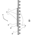
図1を参照すると、一般的に番号10で示される、フリップチップパッケージのような電子アセンブリの断面が示され、この電子アセンブリは基体12を含み、この基体は基体12の底面上に任意のハンダボール13を有する。さらに、電子アセンブリ10はダイのような電子部品14を含み、この電子部品はハンダジョイント15(電子部品14上のハンダバンプと基体12上のボンディングパッドとから形成される)を介して基体12に電気的に接続されており、このハンダジョイントは、電子部品14と基体12との間に配置された硬化したアンダーフィル組成物11を有し、硬化したアンダーフィル組成物11はジビニルアレーンジエポキシドの反応生成物を含む。
Referring to FIG. 1, a cross-section of an electronic assembly, such as a flip chip package, generally indicated by the numeral 10, is shown, which includes a
その最も広い範囲において、本発明は、(a)ジビニルアレーンジオキシド;(b)硬化剤;および(c)任意に触媒;を含む、アンダーフィル封止材において使用するための硬化性エポキシ樹脂組成物または配合物を含む。本発明のエポキシド組成物または配合物には、実施形態として、(1)ジビニルアレーンジオキシドを含む重合可能な硬化性組成物;(2)ジビニルアレーンジオキシドを含む部分的に硬化された組成物;並びに(3)上記(1)および(2)から生じたジビニルアレーンジオキシドを含む硬化した組成物;が挙げられる。本発明は、ジビニルアレーンジオキシドを含む組成物の硬化(すなわち重合)にも関する。さらに、ジビニルアレーンジオキシド中のある水準(約50%未満)の不純物が予想され、これは最終性能にほとんど影響を与えずに存在しうる。 In its broadest scope, the present invention relates to a curable epoxy resin composition for use in an underfill encapsulant comprising (a) divinylarene dioxide; (b) a curing agent; and (c) optionally a catalyst. Product or compound. The epoxide composition or formulation of the present invention includes, as embodiments, (1) a polymerizable curable composition comprising divinylarene dioxide; (2) a partially cured composition comprising divinylarene dioxide. And (3) a cured composition comprising divinylarene dioxide resulting from (1) and (2) above. The present invention also relates to curing (ie, polymerization) of compositions comprising divinylarene dioxide. In addition, certain levels (less than about 50%) of impurities in divinylarene dioxide are expected and can be present with little impact on the final performance.
本発明のアンダーフィル組成物は有利なことに、室温で低粘度で均一な液体、例えば、25℃で5.0Pa・s未満である。未硬化のもしくは硬化したポリマーの物理的特性に様々な改変を提供するために、フィラーのような固体の粒子状物質がアンダーフィル組成物に組み込まれうる。このような添加固体物質が存在するかしないかにかかわらず、この組成物は、高圧、真空補助または高温への加熱を適用する必要なしに(このような手段は所望の場合には使用されうるが)、小さな(例えば、20μm未満)隙間をみたす。アンダーフィル組成物は、壊れやすい電子部品を保護するために利用されることができ、この場合、この組成物は5ppm未満、好ましくは3ppm未満の低い全塩化物含量を示す。「全」塩化物含量は、結合塩化物と加水分解性塩化物含量の双方を含む。 The underfill composition of the present invention is advantageously a low viscosity, uniform liquid at room temperature, for example, less than 5.0 Pa · s at 25 ° C. Solid particulate materials such as fillers may be incorporated into the underfill composition to provide various modifications to the physical properties of the uncured or cured polymer. Regardless of the presence or absence of such added solid materials, the composition can be used without the need to apply high pressure, vacuum assistance or heating to high temperatures (such means can be used if desired). A small gap (for example, less than 20 μm) is observed. The underfill composition can be utilized to protect fragile electronic components, where the composition exhibits a low total chloride content of less than 5 ppm, preferably less than 3 ppm. “Total” chloride content includes both bound chloride and hydrolyzable chloride content.
本発明のアンダーフィル組成物の製造においては、ジビニルアレーンジオキシド(成分(a))は、例えば、2つのビニル基を任意の環位置に有する置換もしくは非置換アレーン核を含むことができる。ジビニルアレーンジオキシドのアレーン部分はベンゼン、置換ベンゼン、環付加(ring−annulated)ベンゼン、置換環付加ベンゼン、同族結合(homologously bonded)ベンゼン、置換同族結合ベンゼンまたはこれらの混合物を含むことができる。ジビニルアレーンジオキシドのジビニルアレーン部分はオルト、メタ、もしくはパラ異性体、またはこれらのいずれかの混合物であることができる。追加の置換基は、飽和アルキル、アリール、ハロゲン、ニトロ、イソシアナートもしくはRO−(ここで、Rは飽和アルキルもしくはアリールであり得る)をはじめとするH2O2耐性基からなることができる。環付加ベンゼンは、例えば、ナフタレン、テトラヒドロナフタレンなどを含むことができる。(置換)同族結合ベンゼンは、例えば、ビフェニル、ジフェニルエーテルなどを含むことができる。 In the production of the underfill composition of the present invention, the divinylarene dioxide (component (a)) can contain, for example, a substituted or unsubstituted arene nucleus having two vinyl groups at any ring position. The arene portion of the divinylarene dioxide can include benzene, substituted benzene, ring-annulated benzene, substituted cycloaddition benzene, homologously bonded benzene, substituted homologous benzene, or mixtures thereof. The divinylarene portion of the divinylarene dioxide can be the ortho, meta, or para isomer, or any mixture thereof. Additional substituents can consist of H 2 O 2 resistant groups including saturated alkyl, aryl, halogen, nitro, isocyanate, or RO—, where R can be saturated alkyl or aryl. Cycloadded benzene can include, for example, naphthalene, tetrahydronaphthalene, and the like. (Substituted) homologous benzene can include, for example, biphenyl, diphenyl ether, and the like.
本発明の組成物の製造に使用されるジビニルアレーンジオキシドは次の化学構造I−IVによって一般的に示されうる:

本発明のジビニルアレーンジオキシドコモノマーの上記構造I、II、IIIおよびIVにおいて、各R1、R2、R3およびR4は個々に、水素、アルキル、シクロアルキル、アリールもしくはアリールアルキル基;またはH2O2−耐性基、例えば、ハロゲン、ニトロ、イソシアナートまたはRO基(Rはアルキル、アリールもしくはアリールアルキルであり得る)であることができ;xは0〜4の整数であり;yは2以上の整数であり;x+yは6以下の整数であり;zは0〜6の整数であり;z+yは8以下の整数であり;Arはアレーンフラグメント、例えば、1,3−フェニレン基である。さらに、R4は反応性基、例えば、エポキシド、イソシアナート、もしくは任意の反応性基であることができ;Zは置換パターンに応じて、0〜6の整数である。 In the above structures I, II, III and IV of the divinylarene dioxide comonomer of the present invention, each R 1 , R 2 , R 3 and R 4 is independently a hydrogen, alkyl, cycloalkyl, aryl or arylalkyl group; or Can be a H 2 O 2 -resistant group, such as a halogen, nitro, isocyanate or RO group (R can be alkyl, aryl or arylalkyl); x is an integer from 0 to 4; y is X + y is an integer of 6 or less; z is an integer of 0-6; z + y is an integer of 8 or less; Ar is an arene fragment, for example, a 1,3-phenylene group . In addition, R 4 can be a reactive group, such as an epoxide, isocyanate, or any reactive group; Z is an integer from 0 to 6 depending on the substitution pattern.
ある実施形態においては、本発明において使用されるジビニルアレーンジオキシドは、例えば、国際公開第2010/077483号に記載される方法によって製造されることができ、この文献は参照によって本明細書に組み込まれる。本発明において有用であるジビニルアレーンジオキシド組成物は、例えば、米国特許第2,924,580号にも開示され、この文献は参照によって本明細書に組み込まれる。 In certain embodiments, the divinylarene dioxide used in the present invention can be produced, for example, by the method described in WO 2010/077483, which is incorporated herein by reference. It is. Divinylarene dioxide compositions useful in the present invention are also disclosed, for example, in US Pat. No. 2,924,580, which is hereby incorporated by reference.
別の実施形態においては、本発明において有用なジビニルアレーンジオキシドには、例えば、ジビニルベンゼンジオキシド、ジビニルナフタレンジオキシド、ジビニルビフェニルジオキシド、またはジビニルジフェニルエーテルジオキシド、およびこれらの混合物を挙げることができる。 In another embodiment, divinylarene dioxide useful in the present invention includes, for example, divinylbenzene dioxide, divinylnaphthalenedioxide, divinylbiphenyldioxide, or divinyldiphenyletherdioxide, and mixtures thereof. it can.
本発明の好ましい実施形態においては、アンダーフィル組成物に使用されるジビニルアレーンジオキシドはジビニルベンゼンジオキシド(DVBDO)を含む。最も好ましくは、ジビニルアレーンジオキシド成分は、下記構造Vの化学式によって表されるジビニルベンゼンジオキシドである:
上記DVBDO化合物の化学式はC10H10O2であり;DVBDOの分子量は162.2であり;DVBDOの元素分析は:C,74.06;H、6.21;およびO、19.73であり、81g/molのエポキシド当量重量を有する。 The chemical formula of the DVBDO compound is C 10 H 10 O 2 ; the molecular weight of DVBDO is 162.2; the elemental analysis of DVBDO is: C, 74.06; H, 6.21; and O, 19.73 Yes, with an epoxide equivalent weight of 81 g / mol.
以下の構造VIは、本発明において有用なDVBDOの好ましい化学構造の実施形態を示す:
以下の構造VIIは、本発明において有用なDVBDOの好ましい化学構造の別の実施形態を示す:
当該技術分野において知られた方法によってDVBDOが製造される場合には、3つの可能な異性体:オルト、メタおよびパラのうちの1つを得ることができる。よって、本発明は、上記構造のいずれか1つによって示されるDVBDOを個々にまたはこれらの混合物として含む。上記構造VIおよびVIIはDVBDOのメタ(1,3−DVBDO)およびパラ異性体をそれぞれ示す。オルト異性体は希であり;通常、DVBDOは、9:1〜1:9の比率の範囲のメタ(構造VI):パラ(構造VII)異性体で一般的に大抵は製造される。一実施形態として、本発明は、好ましくは、6:1〜1:6の比率の範囲の構造VI:構造VIIを含み、別の実施形態においては、構造VI:構造VIIの比率は4:1〜1:4、または2:1〜1:2であることができる。 When DVBDO is produced by methods known in the art, one of three possible isomers can be obtained: ortho, meta and para. Thus, the present invention includes DVBDO represented by any one of the above structures individually or as a mixture thereof. Structures VI and VII above show the meta (1,3-DVBDO) and para isomers of DVBDO, respectively. Ortho isomers are rare; usually DVBDO is generally mostly produced with meta (structure VI): para (structure VII) isomers in the range of 9: 1 to 1: 9 ratios. In one embodiment, the present invention preferably comprises structure VI: structure VII in the range of 6: 1 to 1: 6 ratio, and in another embodiment the ratio of structure VI: structure VII is 4: 1. Can be ˜1: 4, or 2: 1 to 1: 2.
本発明のさらに別の実施形態においては、ジビニルアレーンジオキシドは、ある量(例えば、20重量%未満の量)の置換アレーンを含むことができる。置換アレーンの量および構造は、ジビニルアレーンジオキシドへのジビニルアレーン前駆体の製造に使用される方法に依存する。例えば、ジエチルベンゼン(DEB)の脱水素化によって製造されるジビニルベンゼンはある量のエチルビニルベンゼン(EVB)およびDEBを含むことができる。過酸化水素との反応の際に、EVBはエチルビニルベンゼンモノオキシドを生じさせ、一方DEBは変化しないままである。これらの化合物の存在は、ジビニルアレーンジオキシドのエポキシド当量重量を、純粋な化合物のエポキシド当量重量よりも大きな値まで増大させることができるが、エポキシ樹脂部分の0〜99%の量で利用されうる。 In yet another embodiment of the invention, the divinylarene dioxide can include an amount (eg, less than 20% by weight) of a substituted arene. The amount and structure of the substituted arene depends on the method used to prepare the divinylarene precursor to divinylarene dioxide. For example, divinylbenzene produced by dehydrogenation of diethylbenzene (DEB) can contain certain amounts of ethylvinylbenzene (EVB) and DEB. Upon reaction with hydrogen peroxide, EVB produces ethyl vinylbenzene monooxide, while DEB remains unchanged. The presence of these compounds can increase the epoxide equivalent weight of the divinylarene dioxide to a value greater than the epoxide equivalent weight of the pure compound, but can be utilized in an amount of 0-99% of the epoxy resin portion. .
ある実施形態においては、本発明において有用なジビニルアレーンジオキシドは、例えば、ジビニルベンゼンジオキシド(DVBDO)、低粘度液体エポキシ樹脂を含む。本発明の方法において使用されるジビニルアレーンジオキシドの粘度は、25℃で、概して、0.001Pa・s〜0.1Pa・s、好ましくは、0.01Pa・s〜0.05Pa・s、より好ましくは、0.01Pa・s〜0.025Pa・sである。 In some embodiments, divinylarene dioxide useful in the present invention includes, for example, divinylbenzene dioxide (DVBDO), a low viscosity liquid epoxy resin. The viscosity of the divinylarene dioxide used in the method of the present invention is generally from 0.001 Pa · s to 0.1 Pa · s, preferably from 0.01 Pa · s to 0.05 Pa · s, at 25 ° C. Preferably, it is 0.01 Pa · s to 0.025 Pa · s.
本発明において配合物のエポキシ樹脂部分として使用されるジビニルアレーンオキシドの濃度は、他の配合成分の分率に依存しうるが、一般に、エポキシ樹脂部分は、0.5重量%〜100重量%、好ましくは、1重量%〜99重量%、より好ましくは、2重量%〜98重量%、さらにより好ましくは、5重量%〜95重量%の範囲である。例えば、配合物中のDVBDOの濃度は他の配合成分に依存しうるが、DVBDOの濃度は、一般に、全組成物の重量を基準にして、1重量%〜99重量%、好ましくは、5重量%〜90重量%、最も好ましくは7重量%〜60重量%である。本発明のシステムの一実施形態においては、DVBDOはエポキシ樹脂成分であり、このDVBDOは全組成物の重量を基準にして20重量%〜80重量%の濃度で使用される。 In the present invention, the concentration of divinylarene oxide used as the epoxy resin portion of the formulation may depend on the fraction of other formulation components, but generally the epoxy resin portion is 0.5 wt% to 100 wt%, Preferably, it ranges from 1 wt% to 99 wt%, more preferably from 2 wt% to 98 wt%, even more preferably from 5 wt% to 95 wt%. For example, the concentration of DVBDO in the formulation may depend on other formulation components, but the concentration of DVBDO is generally from 1% to 99%, preferably 5%, based on the weight of the total composition % To 90% by weight, most preferably 7% to 60% by weight. In one embodiment of the system of the present invention, DVBDO is an epoxy resin component, which is used at a concentration of 20% to 80% by weight based on the weight of the total composition.
本発明の最も広い用語においては、硬化剤(架橋剤)または硬化剤ブレンド(硬化剤の混合物)が本発明のアンダーフィル組成物において使用される。一般的に、エポキシ樹脂を硬化(重合)するのに好適であると当該技術分野において知られている何らかの硬化剤が使用されうる。硬化剤の選択は用途の要求に依存しうる。本発明のアンダーフィル組成物において有用な硬化剤には、これらに限定されないが、ジシアンジアミド、置換グアニジン、フェノール系、アミノ、ベンゾオキサジン、無水物、アミド アミン、ポリアミド、ポリアミン、芳香族アミン、ポリエステル、ポリイソシアナート、ポリメルカプタン、尿素ホルムアルデヒドおよびメラミンホルムアルデヒド樹脂、並びにこれらの混合物が挙げられる。ある実施形態においては、本アンダーフィル組成物は無水物を実質的に含まず、好ましくは無水物を含まない。 In the broadest term of the present invention, a curing agent (crosslinking agent) or a curing agent blend (mixture of curing agents) is used in the underfill composition of the present invention. In general, any curing agent known in the art to be suitable for curing (polymerizing) an epoxy resin may be used. The choice of curing agent can depend on the application requirements. Curing agents useful in the underfill composition of the present invention include, but are not limited to, dicyandiamide, substituted guanidine, phenolic, amino, benzoxazine, anhydride, amidoamine, polyamide, polyamine, aromatic amine, polyester, Polyisocyanates, polymercaptans, urea formaldehyde and melamine formaldehyde resins, and mixtures thereof. In some embodiments, the underfill composition is substantially free of anhydride, and preferably free of anhydride.
硬化剤の濃度は、化学量論考慮事項(モル比)に依存しうる。エポキシの硬化剤に対する典型的なモル比は0.25〜4、より好ましくは0.5〜2、最も好ましくは、0.9〜1.1である。 The concentration of curing agent can depend on stoichiometric considerations (molar ratio). A typical molar ratio of epoxy to curing agent is 0.25 to 4, more preferably 0.5 to 2, and most preferably 0.9 to 1.1.
本発明の最も広い用語において、触媒が、場合によって本アンダーフィル組成物において使用されうる。一般的に、エポキシ樹脂と硬化剤との間の反応を容易にするのに好適であると当該技術分野において知られている均一もしくは不均一触媒が使用されうる。この触媒には、これに限定されないが、イミダゾール、第三級アミン、ホスホニウム錯体、ルイス酸またはルイス塩基、遷移金属触媒およびこれらの混合物が挙げられうる。ある実施形態においては、アンダーフィル組成物は、ルイス酸触媒を実質的に含まず、好ましくはルイス酸触媒を含まない。 In the broadest term of the invention, a catalyst may optionally be used in the underfill composition. In general, homogeneous or heterogeneous catalysts known in the art to be suitable for facilitating the reaction between the epoxy resin and the curing agent may be used. The catalyst can include, but is not limited to, imidazoles, tertiary amines, phosphonium complexes, Lewis acids or Lewis bases, transition metal catalysts, and mixtures thereof. In some embodiments, the underfill composition is substantially free of Lewis acid catalyst, and preferably free of Lewis acid catalyst.
本発明において有用な触媒には、例えば、ルイス酸、例えば、三フッ化ホウ素錯体、ルイス塩基、例えば、第三級アミン、ジアザビシクロウンデセンおよび2−フェニルイミダゾール、第四級塩、例えば、臭化テトラブチルホスホニウムおよび臭化テトラエチルアンモニウム、並びにハロゲン化有機アンチモン、例えば、四ヨウ化トリフェニルアンチモンおよび二臭化トリフェニルアンチモン;並びに、これらの混合物が挙げられうる。 Catalysts useful in the present invention include, for example, Lewis acids such as boron trifluoride complexes, Lewis bases such as tertiary amines, diazabicycloundecene and 2-phenylimidazole, quaternary salts such as Mention may be made of tetrabutylphosphonium bromide and tetraethylammonium bromide and organic antimony halides, such as triphenylantimony tetraiodide and triphenylantimony dibromide; and mixtures thereof.
存在する場合には、触媒の濃度は、アンダーフィル組成物の全重量を基準にして、概して、0.05重量%〜10重量%、好ましくは、0.1重量%〜5重量%、最も好ましくは、0.15重量%〜1重量%である。この触媒濃度は、最終用途における適切な処理を可能にするように調節されうる。 When present, the concentration of the catalyst is generally from 0.05 wt% to 10 wt%, preferably from 0.1 wt% to 5 wt%, most preferably, based on the total weight of the underfill composition. Is from 0.15% to 1% by weight. This catalyst concentration can be adjusted to allow for proper processing in the final application.
フィラーは本アンダーフィル組成物に添加されることができ、硬化したシステムの熱機械的特性を向上させ、より良好な部品信頼性性能を付与することができる。フィラーの存在は硬化したアンダーフィルの弾性率を増大させ、かつ電子部品と基体とのCTEをより良好に適合させるために、接着剤(硬化したアンダーフィル)のCTEを低減させる。例えば、配合物は1種以上の任意の官能性もしくは非官能性フィラー、例えば、溶融シリカ、天然シリカ、合成シリカ、天然酸化アルミニウム、合成酸化アルミニウム、中空フィラー、アルミニウムトリヒドロキシド、アルミニウムヒドロキシドオキシド、窒化ホウ素、炭化ケイ素、マイカ、アルミニウム粉体、酸化亜鉛、銀、グラファイト、窒化アルミニウム、ムライト、金、炭素、炭素ナノチューブ、グラファイト、ガラス繊維/シート、炭素繊維、または他の有機もしくは無機粒子状フィラーを含むことができ、配合物にその最終状態で添加されることができ、またはその場で形成されうる。シリカは、溶融、天然または合成にかかわらず好ましいフィラーである。フィラーの表面は場合によっては、フィラーおよびポリマー相互作用を向上させるために処理されることができる。別の実施形態においては、アンダーフィル組成物において使用されるDVBDOブレンドへのシリカフィラーの添加は、最終の硬化したアンダーフィル物質の破壊靱性を増大させうる。 Fillers can be added to the underfill composition to improve the thermomechanical properties of the cured system and to provide better component reliability performance. The presence of the filler increases the elastic modulus of the cured underfill and reduces the CTE of the adhesive (cured underfill) in order to better match the CTE between the electronic component and the substrate. For example, the formulation may include one or more optional functional or non-functional fillers such as fused silica, natural silica, synthetic silica, natural aluminum oxide, synthetic aluminum oxide, hollow filler, aluminum trihydroxide, aluminum hydroxide oxide Boron nitride, silicon carbide, mica, aluminum powder, zinc oxide, silver, graphite, aluminum nitride, mullite, gold, carbon, carbon nanotubes, graphite, glass fiber / sheet, carbon fiber, or other organic or inorganic particulates Fillers can be included, added to the formulation in its final state, or formed in situ. Silica is a preferred filler, whether molten, natural or synthetic. The surface of the filler can optionally be treated to improve the filler and polymer interaction. In another embodiment, the addition of silica filler to the DVBDO blend used in the underfill composition can increase the fracture toughness of the final cured underfill material.
フィラー物質の許容されうる粒子サイズは、一般に、ナノから従来のマイクロサイズの範囲であることができる。例えば、フィラーの粒子サイズは0.0005μm〜500μm、好ましくは、0.100μm〜100μm、より好ましくは、0.01μm〜30μmの範囲であることができる。 Acceptable particle sizes for filler materials can generally range from nano to conventional microsize. For example, the particle size of the filler can be in the range of 0.0005 μm to 500 μm, preferably 0.100 μm to 100 μm, more preferably 0.01 μm to 30 μm.
許容できるフィラー形態には、これに限定されないが、プレートレット(platelet)、繊維状、球状、針状、非晶質またはこれらの任意の組み合わせが挙げられる。異なるサイズおよび異なる形状を有するフィラーは、熱膨張係数、弾性率、電気伝導率および/または熱伝導率について相乗的な効果を有するように組み合わせられうる。 Acceptable filler forms include, but are not limited to, platelets, fibrous, spherical, acicular, amorphous, or any combination thereof. Fillers having different sizes and different shapes can be combined to have a synergistic effect on thermal expansion coefficient, elastic modulus, electrical conductivity and / or thermal conductivity.
本発明において利用されるフィラーは、アンダーフィル組成物への組み込み前に、または配合物のコンパウンディング中に、その場で、場合によっては、表面処理されることができる。表面処理剤の例には、脂肪酸、シランカップリング剤、チタナート、ジルコナートまたはシラザン化合物が挙げられる。 The filler utilized in the present invention can optionally be surface treated in situ, prior to incorporation into the underfill composition, or during compounding of the formulation. Examples of the surface treatment agent include fatty acid, silane coupling agent, titanate, zirconate or silazane compound.
本発明において有用なフィラー添加量は変動しうる。フィラーの濃度は、組成物中の固形分の重量を基準にして、一般に0重量%〜99重量%、好ましくは、0.1重量%〜95重量%、より好ましくは、10重量%〜90重量%、最も好ましくは、50重量%〜80重量%である。体積添加量は、望まれる特性に応じて、0〜90体積%、より好ましくは、0.1〜90体積%、さらにより好ましくは85体積%以下、さらにより好ましくは0.1〜85体積%、さらにより好ましくは1〜85体積%、および最も好ましくは1〜70体積%の範囲であり得る。 The amount of filler added useful in the present invention can vary. The filler concentration is generally 0% to 99% by weight, preferably 0.1% to 95% by weight, more preferably 10% to 90% by weight, based on the weight of solids in the composition. %, Most preferably from 50% to 80% by weight. Depending on the properties desired, the volume addition is 0-90% by volume, more preferably 0.1-90% by volume, even more preferably 85% by volume or less, and even more preferably 0.1-85% by volume. Even more preferably, it can range from 1 to 85% by volume, and most preferably from 1 to 70% by volume.
従来のエポキシベースのアンダーフィル組成物において必要とされる高いフィラー添加量は、アンダーフィル組成物の粘度を非常に増大させること、電子部品と基体との間の組成物の流動性を低減させること、並びに、より高い適用温度を必要とすることなどの多くの技術的困難性をもたらすことが周知である。そもそも収縮するハンダバンプおよびボンディングパッドのピッチサイズはこの困難性を悪化させる。本アンダーフィル組成物は、比較的高いフィラー添加量においてさえ、低い粘度および優れた流動性を示すことが見いだされた。特に、本発明は、ジビニルアレーンジエポキシド、硬化剤およびフィラーを含む組成物であって、フィラーが組成物の全体積を基準にして1〜70体積%の量で存在する場合、25℃で0.005〜100Pa・sの粘度を有する組成物を提供する。好ましくは、フィラーが1〜70体積%の量で存在する場合、組成物は25℃で0.01〜25Pa・s、より好ましくは25℃で0.01〜10Pa・sの粘度を有する。特に好ましい実施形態においては、フィラーが50〜70体積%の量で存在する場合、組成物は25℃で0.005〜1Pa・sの粘度を有する。このような組成物においてジビニルアレーンジエポキシドはジビニルベンゼンジオキシドであることが好ましい。本アンダーフィル組成物のさらなる利点は、従来のアンダーフィル組成物より有意に低い、室温でまたは室温付近でこれが適用されうることである。 The high filler loading required in conventional epoxy-based underfill compositions greatly increases the viscosity of the underfill composition and reduces the fluidity of the composition between the electronic component and the substrate. As well as many technical difficulties such as requiring higher application temperatures. The shrinking solder bump and bond pad pitch sizes exacerbate this difficulty. The underfill composition has been found to exhibit low viscosity and excellent flow even at relatively high filler loadings. In particular, the present invention is a composition comprising divinylarene diepoxide, a curing agent and a filler, wherein the filler is present at 0 ° C. at 25 ° C. A composition having a viscosity of 0.005 to 100 Pa · s is provided. Preferably, when the filler is present in an amount of 1 to 70% by volume, the composition has a viscosity of 0.01 to 25 Pa · s at 25 ° C, more preferably 0.01 to 10 Pa · s at 25 ° C. In a particularly preferred embodiment, the composition has a viscosity of 0.005 to 1 Pa · s at 25 ° C. when the filler is present in an amount of 50 to 70% by volume. In such compositions, the divinylarene diepoxide is preferably divinylbenzene dioxide. A further advantage of the present underfill composition is that it can be applied at or near room temperature, significantly lower than conventional underfill compositions.
本発明のアンダーフィル組成物は、有利に、多様な硬化剤を使用することができ、本組成物は、従来のアンダーフィル組成物よりも、ナノフィラーのようなフィラーの、より多くの選択肢を可能にし、よって、本発明の組成物の配合オプションを広くする。本アンダーフィル組成物は、また、全ハロゲン化物を少ししか有しない(例えば、5ppm未満)、または全く有しない。さらに、本アンダーフィル組成物は高いフィラー添加量も可能にするので、本アンダーフィル組成物は、適用中同じ流速で、より低いCTE(例えば、Tg未満で、30ppm/℃未満)もしくはより良好な熱伝導率(例えば、1.0W/mK超)を達成しうるか、または同じCTEもしくは熱伝導率でより良好な流速を達成することができる。 The underfill composition of the present invention can advantageously use a variety of curing agents, and the composition provides more options for fillers such as nanofillers than conventional underfill compositions. And thus broaden the formulation options of the composition of the present invention. The underfill composition also has little (eg, less than 5 ppm) or no total halide. In addition, since the underfill composition also allows for high filler loading, the underfill composition has a lower CTE (eg, less than 30 ppm / ° C. below Tg) or better at the same flow rate during application. Thermal conductivity (eg, greater than 1.0 W / mK) can be achieved, or better flow rates can be achieved with the same CTE or thermal conductivity.
本アンダーフィル組成物において有用であり得る他の任意成分は、当業者に知られている樹脂配合物において通常使用される成分である。例えば、任意成分は、適用特性(例えば、表面張力改変剤または流動助剤)、信頼性特性(例えば、接着促進剤)、反応速度、反応の選択性および/または触媒寿命を増大させるために組成物に添加されうる化合物を含むことができる。 Other optional ingredients that may be useful in the present underfill composition are those commonly used in resin formulations known to those skilled in the art. For example, optional ingredients may be formulated to increase application properties (eg, surface tension modifiers or flow aids), reliability properties (eg, adhesion promoters), reaction rates, reaction selectivity and / or catalyst life. It can contain compounds that can be added to the product.
様々な添加剤、例えば、ジビニルアレーンジオキシドとは異なるエポキシ樹脂のような他の樹脂、成分(a)、希釈剤、安定化剤、フィラー、可塑剤、触媒不活性化剤、強化剤など、並びにこれらの混合物などが本発明の組成物に添加されることができる。 Various additives such as other resins such as epoxy resins different from divinylarene dioxide, component (a), diluents, stabilizers, fillers, plasticizers, catalyst deactivators, reinforcing agents, etc. In addition, a mixture thereof can be added to the composition of the present invention.
本発明の配合物において有用な他の添加剤には、例えば、ハロゲン含有もしくはハロゲン非含有難燃剤;消火能力の性能を向上させるための相乗剤、例えば、水酸化マグネシウム、ホウ酸亜鉛、またはメタロセン;処理性のための溶媒、例えば、アセトン、メチルエチルケトン、ダウアノール(Dowanol)PMA;接着促進剤、例えば、修飾有機シラン(エポキシ化、メタクリル、アミノ)、アセチルアセトナート、または硫黄含有分子;湿潤剤および分配剤、例えば、修飾有機シラン、バイク(Byk)900シリーズおよびBykW−9010、修飾フルオロカーボン;空気放出添加剤、例えば、Byk−A530、Byk−A525、Byk−A555、Byk−A560;表面修飾剤、例えば、スリップ添加剤および光沢添加剤(その多くはバイクキミー(Byk−Chemie)から入手可能である);反応性もしくは非反応性熱可塑性樹脂、例えば、ポリフェニルスルホン、ポリスルホン、ポリエーテルスルホン、ポリフッ化ビニリデン、ポリエーテルイミド、ポリフタルイミド、ポリベンズイミダゾール、アクリル、フェノキシ、ウレタン;離型剤、例えば、ワックス;他の官能性添加剤またはポリマー特性を改良するためにあらかじめ反応された生成物、例えば、イソシアナート、イソシアヌラート、シアナートエステル、アリル含有分子または他のエチレン性不飽和化合物、およびアクリラート;並びにこれらの混合物が挙げられる。 Other additives useful in the formulations of the present invention include, for example, halogen-containing or non-halogen-containing flame retardants; synergists to improve fire fighting performance, such as magnesium hydroxide, zinc borate, or metallocene Solvents for processability, such as acetone, methyl ethyl ketone, Dowanol PMA; adhesion promoters, such as modified organosilanes (epoxidation, methacryl, amino), acetylacetonate, or sulfur containing molecules; wetting agents and Distributing agents such as modified organosilanes, Byk 900 series and BykW-9010, modified fluorocarbons; air release additives such as Byk-A530, Byk-A525, Byk-A555, Byk-A560; surface modifiers, For example, slip additives and gloss additives (Many of which are available from Byk-Chemie); reactive or non-reactive thermoplastics such as polyphenylsulfone, polysulfone, polyethersulfone, polyvinylidene fluoride, polyetherimide, polyphthalimide, Polybenzimidazole, acrylic, phenoxy, urethane; mold release agents such as waxes; other functional additives or pre-reacted products to improve polymer properties such as isocyanates, isocyanurates, cyanates Esters, allyl-containing molecules or other ethylenically unsaturated compounds, and acrylates; and mixtures thereof.
本発明において使用される任意の添加剤の濃度は、概して0重量%〜99重量%、好ましくは0.001重量%〜95重量%、より好ましくは0.01重量%〜60重量%、および最も好ましくは0.05重量%〜50重量%の範囲であり得る。 The concentration of any additive used in the present invention is generally 0% to 99% by weight, preferably 0.001% to 95%, more preferably 0.01% to 60%, and most Preferably it may be in the range of 0.05 wt% to 50 wt%.
本発明に従ってアンダーフィル組成物として使用することが意図される配合物の一般的な例として、アンダーフィル配合物は以下の成分をそのそれぞれの量で含むことができる:
半導体パッケージング物質の製造に有用な、低粘度(例えば、25℃で3.0Pa・s未満)で、低い全塩化物含有(例えば5ppm未満)のエポキシ樹脂配合物の製造方法は、(a)ジビニルベンゼンジオキシド;(b)硬化剤;(c)場合によって、触媒;および(d)場合によって、必要とされる他の成分:をブレンドすることを含む。例えば、本発明の硬化性エポキシ樹脂配合物の製造は、ロス(Ross)PDミキサー(チャールスロス;Charles Ross)において真空を用いてまたは真空を用いずに、ジビニルベンゼンジオキシド、硬化剤、触媒および場合によって何らかの他の所望の添加剤をブレンドすることにより達成される。場合によって補充される上述の配合添加剤のいずれか、例えば、フィラーは、組成物を形成するために、混合中にまたは混合前に組成物に添加されることもできる。 A method for producing a low viscosity (eg, less than 3.0 Pa · s at 25 ° C.) and low total chloride content (eg, less than 5 ppm) epoxy resin formulation useful in the manufacture of semiconductor packaging materials comprises (a) Blending divinylbenzene dioxide; (b) curing agent; (c) optionally a catalyst; and (d) optionally other components required. For example, the preparation of the curable epoxy resin formulation of the present invention can be accomplished using divinylbenzene dioxide, a curing agent, a catalyst and a catalyst in a Ross PD mixer (Charles Ross) with or without vacuum. Optionally achieved by blending with some other desired additive. Any of the above-described formulation additives, optionally supplemented, such as fillers, can also be added to the composition during or before mixing to form the composition.
エポキシ樹脂配合物の全ての成分は典型的には、所望の用途に効果的な低い粘度を有するエポキシ樹脂組成物の製造を可能にする温度で混合され、分散される。全ての成分の混合中の温度は、概して、20℃〜80℃、好ましくは、25℃〜35℃であることができる。より低い混合温度は、樹脂と硬化剤成分との反応を最小限にし、配合物のポットライフを最大化するのを助ける。 All components of the epoxy resin formulation are typically mixed and dispersed at a temperature that allows for the production of an epoxy resin composition having a low viscosity effective for the desired application. The temperature during the mixing of all components can generally be between 20 ° C and 80 ° C, preferably between 25 ° C and 35 ° C. The lower mixing temperature helps minimize the reaction of the resin with the hardener component and maximize the pot life of the formulation.
ブレンドされた化合物は典型的には周囲温度以下の温度で貯蔵され、貯蔵寿命を最大化する。許容可能な温度範囲は、例えば、−100℃〜25℃、より好ましくは、−70℃〜10℃、さらにより好ましくは、−50℃〜0℃である。ある実施形態の例として、その温度は−40℃でありうる。 Blended compounds are typically stored at sub-ambient temperatures to maximize shelf life. The allowable temperature range is, for example, -100 ° C to 25 ° C, more preferably -70 ° C to 10 ° C, and even more preferably -50 ° C to 0 ° C. As an example of an embodiment, the temperature can be −40 ° C.
本発明のエポキシ樹脂である、ジビニルベンゼンジオキシド(DVBDO)は単独の樹脂として使用されて、最終配合物においてエポキシマトリックスを形成することができるか;またはジビニルベンゼンジオキシド樹脂は最終配合物中の成分のうちの1つとして使用されうる。例えば、エポキシ樹脂は添加希釈剤として使用されうる。ジビニルベンゼンジオキシドの使用は、硬化性組成物および最終硬化生成物に、従来のグリシジルエーテル、グリシジルエステルまたはグリシジルアミンエポキシ樹脂を超える改良された特性を付与する。特に、DVBDOの使用は、相対的に高いフィラー添加量を可能にする一方で、25℃での相対的に低い粘度を維持する。 The epoxy resin of the present invention, divinylbenzene dioxide (DVBDO), can be used as a single resin to form an epoxy matrix in the final formulation; or the divinylbenzene dioxide resin is in the final formulation. It can be used as one of the components. For example, epoxy resins can be used as additive diluents. The use of divinylbenzene dioxide imparts improved properties to curable compositions and final cured products over conventional glycidyl ethers, glycidyl esters or glycidylamine epoxy resins. In particular, the use of DVBDO allows a relatively high filler loading while maintaining a relatively low viscosity at 25 ° C.
さらに、ジビニルベンゼンジオキシドの使用は、望ましく低い全ハロゲン含量から全ハロゲン含量ゼロをもたらし、高湿度試験およびデバイスの寿命にわたる現場使用における電子アセンブリの性能の信頼性を維持する。このハロゲン含量、例えば、塩素含量は概して、500ppm未満;好ましくは、100ppm未満;およびより好ましくは、5ppm未満である。 Furthermore, the use of divinylbenzene dioxide results in a desirably low total halogen content to zero total halogen content, maintaining the reliability of electronic assembly performance in high humidity testing and field use over the lifetime of the device. This halogen content, eg chlorine content, is generally less than 500 ppm; preferably less than 100 ppm; and more preferably less than 5 ppm.
本発明の硬化したアンダーフィル組成物(すなわち、硬化性組成物から製造された架橋した生成物)は、硬化した従来のエポキシベースのアンダーフィルよりも改良されたいくつかの特性を示す。例えば、本発明の硬化したアンダーフィルは−55℃〜300℃のガラス転移温度(Tg)を有することができる。概して、この樹脂のTgは−60℃よりも高く、好ましくは0℃よりも高く、より好ましくは10℃よりも高く、より好ましくは25℃よりも高く、最も好ましくは50℃よりも高い。−55℃未満では、本出願に記載された技術は、先行技術に記載された従来の技術に対する何らのさらなる有意な利点を提供せず;200℃より高い場合には、本出願に記載された技術は、概して、強靱化技術を包含することなく、非常にもろいネットワークをもたらし、これは本出願の範囲内の用途には好適ではなく、かつ低温(例えば、0℃未満)でのデバイスの有意な反りももたらしうるであろう。好ましくは、本発明の硬化したアンダーフィル組成物は、ASTM D3418で、25〜300℃、より好ましくは50〜250℃、最も好ましくは50〜225℃のガラス転移温度を示す。 The cured underfill composition of the present invention (ie, the cross-linked product made from the curable composition) exhibits several properties that are improved over cured conventional epoxy-based underfills. For example, the cured underfill of the present invention can have a glass transition temperature (Tg) of -55 ° C to 300 ° C. Generally, the Tg of this resin is higher than −60 ° C., preferably higher than 0 ° C., more preferably higher than 10 ° C., more preferably higher than 25 ° C., and most preferably higher than 50 ° C. Below −55 ° C., the techniques described in this application do not provide any further significant advantages over the prior art described in the prior art; The technology generally results in a very fragile network that does not encompass toughening technology, which is not suitable for applications within the scope of this application and is significant for devices at low temperatures (eg, below 0 ° C.). It can also cause warping. Preferably, the cured underfill composition of the present invention exhibits a glass transition temperature of 25-300 ° C, more preferably 50-250 ° C, and most preferably 50-225 ° C according to ASTM D3418.
ビニル基のエポキシ化中のエピクロロヒドリンの除去のせいで、樹脂中に存在する加水分解性塩化物もしくは全塩化物はほとんどからまったく存在しない。よって、本発明のアンダーフィル組成物は、約60メッシュ粒子の120℃で24時間のパールボム(Parr bomb)抽出後のイオンクロマトグラフィーによって、0.00001〜5000ppm、好ましくは0.00001〜100ppm、最も好ましくは5ppm未満の加水分解性塩化物含量を示す。 Due to the removal of epichlorohydrin during the epoxidation of vinyl groups, there is little to no hydrolyzable chloride or total chloride present in the resin. Thus, the underfill composition of the present invention is 0.00001-5000 ppm, preferably 0.00001-100 ppm, most preferably by ion chromatography after extraction of about 60 mesh particles at 120 ° C. for 24 hours with Parr bomb. Preferably it has a hydrolyzable chloride content of less than 5 ppm.
以下の構造は、より高い水準の全塩化物および加水分解性塩化物含量をもたらす従来のグリシジルエーテル樹脂の反応において形成される、様々な生成物および副生成物を示す:
本発明の硬化したアンダーフィル組成物は、1.0MPa・m1/2より高い、好ましくは1.7MPa・m1/2より高い、より好ましくは2.0MPa・m1/2(メガパスカルパーメートル)より高い、ASTM D5045(室温)によって測定される破壊靱性値を示す。 The cured underfill composition of the present invention is higher than 1.0 MPa · m 1/2, preferably greater than 1.7 MPa · m 1/2, more preferably 2.0 MPa · m 1/2 (MPa par Figure 2 shows fracture toughness values measured by ASTM D5045 (room temperature) higher than metric).
本発明の硬化したアンダーフィル組成物は、ASTM D790によって、Tg未満で、1GPaを超える、好ましくは2GPaを超える、より好ましくは3.5MPa〜15GPaの曲げ弾性率を示す。 The cured underfill composition of the present invention exhibits a flexural modulus of less than Tg, greater than 1 GPa, preferably greater than 2 GPa, more preferably 3.5 MPa to 15 GPa, according to ASTM D790.
本発明の硬化したアンダーフィル組成物は、ASTM D5335によって、Tg未満で、65ppm/℃、好ましくは50ppm/℃未満のCTEを示す。 The cured underfill composition of the present invention exhibits a CTE of less than Tg and less than 65 ppm / ° C, preferably less than 50 ppm / ° C, according to ASTM D5335.
本発明の硬化したアンダーフィル組成物は、ASTM E1131に従った熱質量分析によって、硬化中に10パーセント未満の重量損失を示す。 The cured underfill composition of the present invention exhibits a weight loss of less than 10 percent during cure by thermal mass spectrometry according to ASTM E1131.
ある実施形態においては、ジビニルアレーンのジエポキシド誘導体を使用する本発明のエポキシ樹脂配合物は、半導体パッケージング物質のためのキャピラリーアンダーフィル封止材として使用されうる。このエポキシ樹脂配合物の使用は相対的に高いフィラー添加量(例えば、30体積%より多い、例えば、30〜85体積%)、硬化後の高いTg値(例えば、90℃を超える)、および樹脂によって付与される非常に低いからゼロの全塩化物汚染(例えば5ppm未満)を可能にする。さらに、従来の低粘度環式脂肪族エポキシ樹脂とは異なり、この樹脂は多くの様々な硬化剤が使用されるのを可能にする。比較的低い塩化物汚染は、ハロゲン化中間体、例えば、エピクロロヒドリンを利用しない分子を製造する合成径路に起因する。 In certain embodiments, the epoxy resin formulation of the present invention using a diepoxide derivative of divinylarene can be used as a capillary underfill encapsulant for semiconductor packaging materials. The use of this epoxy resin formulation is relatively high filler loading (eg, greater than 30% by volume, eg, 30-85% by volume), high Tg value after curing (eg, greater than 90 ° C.), and resin Allows very low to zero total chloride contamination (eg less than 5 ppm) imparted by Furthermore, unlike conventional low viscosity cycloaliphatic epoxy resins, this resin allows many different curing agents to be used. The relatively low chloride contamination is due to synthetic pathways that produce molecules that do not utilize halogenated intermediates such as epichlorohydrin.
以下の実施例および比較例は本発明を詳細にさらに説明するが、その範囲を限定すると解釈されるものではない。 The following examples and comparative examples further illustrate the present invention in detail but are not to be construed as limiting its scope.
実施例1−3、並びに比較例AおよびB
鍵となる目的の特性に対するフィラー添加量および樹脂の影響について検討するために、一組の実験が構築された。比較例AおよびB、並びに実施例1〜3は以下の手順に従って製造された:
各組成物の成分が蓋付きの75ミリリットル(mL)ポリプロピレンプラスチックジャーに入れられ、フラックテック(FlackTek)によるスピードミキサー(SpeedMixer(登録商標))DAC150を用いて、分あたり3200回転(rpm)で120秒間ブレンドされた。フィラー添加量レベルは固形分基準で、35重量%、50重量%、および65重量%であった。実験デザインは可変物として樹脂タイプも含んでおり、D.E.R.商標354(平均エポキシ当量重量(EEW)174g/molのビスフェノールFベースのエポキシ樹脂;ザダウケミカルカンパニーから入手可能)およびジビニルベンゼンジオキシド(DVBDO)を使用した。芳香族アミン硬化剤あるジエチルトルエンジアミン(DETDA)と1:1の化学量論バランスを維持しつつ、2種類の樹脂を1:1の重量比で一緒にした中心点が含まれていた。
Examples 1-3 and Comparative Examples A and B
A set of experiments was constructed to examine the effects of filler loading and resin on key target properties. Comparative Examples A and B, and Examples 1-3 were prepared according to the following procedure:
Components of each composition is placed in 75 ml (mL) polypropylene plastic jar with a lid, a speed mixer by Flacktek (FlackTek) (SpeedMixer (TM)) DAC 150 using a 3200 rotation per minute (rpm) 120 Blended for seconds. Filler addition levels were 35 wt%, 50 wt%, and 65 wt% based on solids. The experimental design includes a resin type as a variable. E. R. Trademark 354 (average epoxy equivalent weight (EEW) 174 g / mol bisphenol F based epoxy resin; available from Sadau Chemical Company) and divinylbenzene dioxide (DVBDO) were used. A central point was included that brought the two resins together in a 1: 1 weight ratio while maintaining a 1: 1 stoichiometric balance with the aromatic amine curing agent diethyltoluenediamine (DETDA).
これらの実施例において使用される他の原料は次のように記載される:エタキュア(Ethacure)100はアルベマーレコーポレーション(Albemarle Corporation)から商業的に入手可能なDETDAであり;Byk−A530は、ドイツ、バイクキミーGmbHによって製造されているポリシロキサン消泡剤であり;Byk W996は、ドイツ、バイクキミーGmbHによって製造されている、酸性基を有するコポリマー(酸価71mgKOH/g)である湿潤剤であり;シランZ−6040は、ダウコーニングによって製造されているエポキシ官能性シランカップリング剤であり;モダフロー(Modaflow)は、シーテックサーフェススペシャリティーズ(Ctyec Surface Specialties)によって製造されている表面張力改変剤/流動助剤であり;およびデンカFB−1SDXは、日本の電気化学工業株式会社によって製造されている、約1.5ミクロンの平均粒子サイズを有する溶融合成球状シリカ粉体である。コート(Coat)O Sil 2810は、モメンティブ(Momentive)からのエポキシ末端ポリジメチルシロキサンである。ジェフアミン(Jeffamine(登録商標))D230はハンツマンコーポレーション(Hunstman Corporation)からのポリエーテルアミンである。アミキュア(Amicure)PACMは、エアプロダクツ(Air Products(登録商標))からの、環式脂肪族アミンである。MP15EFおよびMP8FSは株式会社龍森から入手可能なシリカフィラーである。リーガル(Regal)400Rはカボットコーポレーション(Cabot Corporation)からのある等級のカーボンブラックである。シルウェット(Silwet)L−7608は、モメンティブパフォーマンスマテリアルズ(Momentive Performance Materials)からの有機シリコーン表面張力改変剤である。 Other ingredients used in these examples are described as follows: Ethacure 100 is DETDA commercially available from Albemarle Corporation; Byk-A530 is Germany Byk W996 is a wetting agent that is a copolymer with acidic groups (acid number 71 mg KOH / g), manufactured by Bike Kimmy GmbH, Germany. Z-6040 is an epoxy functional silane coupling agent manufactured by Dow Corning; Modaflow is a Ctyec Surface Specials Ties) is a surface tension modifier / flow aid manufactured by; and Denka FB-1SDX is a melt having an average particle size of about 1.5 microns manufactured by Denki Kagaku Kogyo Co., Ltd., Japan Synthetic spherical silica powder. Coat O Sil 2810 is an epoxy-terminated polydimethylsiloxane from Momentive. Jeffamine (R) D230 is a polyetheramine from Huntsman Corporation. AMICURE (Amicure) PACM is from Air Products (Air Products (R)), a cyclic aliphatic amine. MP15EF and MP8FS are silica fillers available from Tatsumori Corporation. Regal 400R is a grade of carbon black from Cabot Corporation. Silwet L-7608 is an organosilicone surface tension modifier from Momentive Performance Materials.
スピードミキサー中でブレンドし、真空オーブン中で15分間約3000Paで脱ガスした後、8グラム(g)の各サンプルが別個のアルミニウム秤量皿に置かれた。この皿は150℃のオーブン中に60分間配置され、次いで、175℃のオーブン中に90分間配置された。冷却した後、サンプル(スラッジ)はアルミニウム皿から取り出され、べーラーイソメット(Buehler Isomet)1000ソウを用いて切断された。約3mm×3mmの小さなサンプルが各スラッジから切り出され、3mmのプローブを取り付けたTAインスツルメンツ(Instruments)Q400熱機械的分析機を用いて、熱機械的分析(TMA)で分析された。この分析手順は以下の1つの要素からなっていた:室温(約25℃)から275℃への10℃/分の勾配、0.05Nの力で、50mL/分の窒素パージを伴っていた。ユニバーサルアナリシス(Universal Analysis)データ分析ソフトウェア(TAインスツルメンツから市販)が、次いで、利用されて、分析されるサンプルについて、ガラス転移温度(Tg)(オンセット)を決定し、およびTg未満でのCTE(α1 CTE)を決定した。 After blending in a speed mixer and degassing in a vacuum oven for 15 minutes at about 3000 Pa, 8 grams (g) of each sample was placed in a separate aluminum weighing pan. The dish was placed in a 150 ° C. oven for 60 minutes and then placed in a 175 ° C. oven for 90 minutes. After cooling, the sample (sludge) was removed from the aluminum pan and cut using a Bühler Isomet 1000 saw. A small sample of about 3 mm × 3 mm was cut from each sludge and analyzed by thermomechanical analysis (TMA) using a TA Instruments Q400 thermomechanical analyzer fitted with a 3 mm probe. This analytical procedure consisted of one element: a 10 ° C./min gradient from room temperature (about 25 ° C.) to 275 ° C., with a force of 0.05 N and a nitrogen purge of 50 mL / min. Universal Analysis data analysis software (commercially available from TA Instruments) is then utilized to determine the glass transition temperature (Tg) (onset) and CTE below Tg for the sample to be analyzed ( α1 CTE) was determined.
ブレンドされたサンプルの粘度対温度は、35mm上部プレートおよび50mm下部プレートを備え付けたTAインスツルメンツARESアナライザー(TAインスツルメンツ)を用いて測定された。この試験手順は、5℃/分勾配率での25℃〜250℃の動的温度勾配からなっていた。 The viscosity of the blended sample versus temperature was measured using a TA Instruments ARES analyzer (TA Instruments) equipped with a 35 mm top plate and a 50 mm bottom plate. This test procedure consisted of a dynamic temperature gradient from 25 ° C. to 250 ° C. at a rate of 5 ° C./min.
以下の表IIはモデルのアンダーフィル配合物について集められたデータのまとめを含む。注目すべきは、高いTgおよび低い粘度の組み合わせである。DVBDOベースのサンプルのTMAでのTgは、D.E.R.商標354を用いて造られたものよりも約70℃高い。さらに、65%フィラー添加量でのDVBDOサンプルの最小粘度はD.E.R.354を用いて造られたサンプルの20%である。また注目すべきは、触媒の使用のないD.E.R.354システムの相対的に低いTgである。 Table II below contains a summary of the data collected for the model underfill formulation. Of note is a combination of high Tg and low viscosity. The Tg of the DVBDO based sample in TMA is E. R. About 70 ° C. higher than that made using trademark 354. Furthermore, the minimum viscosity of the DVBDO sample at 65% filler loading is D.P. E. R. 20% of the sample made with 354. It should also be noted that D. without the use of a catalyst. E. R. The relatively low Tg of the 354 system.
実施例4〜10は、実施例1〜3に記載されたのと同じ手順を用いて行われ;次の原料を含んでいた。ジオキシドであるDVBDOはザダウケミカルカンパニーから入手可能;ポリアミド硬化剤であるアンカミド(Ancamide(登録商標))506はエアプロダクツから市販されている;ポリエーテルアミンであるジェフアミン(Jeffamine(登録商標))D230はハンツマンコーポレーションから市販されている;シラザンZ−6079(ヘキサメチルジシラザン)はダウコーニングから市販されている;シリカフィラーであるMP−15EFは日本国の株式会社龍森から市販されている;およびエポキシシランであるシランZ−6040はダウコーニングから市販されている。
表IIIに記載される実施例4〜10の配合物は、以下の手順に従ってスピードミキサー(SpeedMixer(登録商標))DAC150(フラックテック(FlackTek)、ランドラム、サウスカロライナ州)を用いてブレンドされた。
Examples 4-10 were carried out using the same procedure as described in Examples 1-3; A-dioxide DVBDO is available from The Dow Chemical Company; a polyamide curing agent Ankamido (Ancamide (R)) 506 is commercially available from Air Products; polyether amines JEFFAMINE (Jeffamine (R)) D230 is commercially available from Huntsman Corporation; silazane Z-6079 (hexamethyldisilazane) is commercially available from Dow Corning; silica filler MP-15EF is commercially available from Tatsumori Corporation in Japan; Silane Z-6040, which is an epoxy silane, is commercially available from Dow Corning.
Formulations of Examples 4-10 set forth in Table III, the following speed mixer according to the procedure (SpeedMixer (TM)) DAC 150 (Flacktek (FlackTek), Landrum, South Carolina) was blended with.
DVBDOおよびMP 15EFを75mLの蓋付きポリプロピレンジャーに入れた。3500rpmで50秒間混合した。シランZ−6079を添加し、3500rpmで120秒間混合した。硬化剤およびシラン6040を添加し、3500rpmで60秒間混合した。次いで、真空オーブン内に25℃で約3000Paで15分間おいて、サンプルを脱ガスした。 DVBDO and MP 15EF were placed in a 75 mL lidded polypropylene jar. Mix for 50 seconds at 3500 rpm. Silane Z-6079 was added and mixed at 3500 rpm for 120 seconds. Curing agent and silane 6040 were added and mixed for 60 seconds at 3500 rpm. The sample was then degassed in a vacuum oven at 25 ° C. and about 3000 Pa for 15 minutes.
最終の混合工程の後で、配合物のサンプルはTAインスツルメンツAR2000レオメーターを用いて分析された。このレオメーターには60mm、1度の円錐が取り付けられていた。試験手順は、10sec−1で30秒間の予備剪断、次いで10sec−1で120秒間保持し、両方の工程は25℃であり、2秒ごとのデータ点で記録することからなっていた。報告される粘度値は最後の10コのデータ点の平均である。 After the final mixing step, a sample of the formulation was analyzed using a TA Instruments AR2000 rheometer. The rheometer was fitted with a 60 mm, 1 degree cone. The test procedure consisted of pre-shearing at 10 sec −1 for 30 seconds, then holding at 10 sec −1 for 120 seconds, both steps at 25 ° C. and recording at data points every 2 seconds. The reported viscosity value is the average of the last 10 data points.
それぞれのサンプルの約9gがアルミニウム秤量皿に注がれ、85℃で45分間、次いで175℃45分間で硬化された。硬化されたサンプルはオーブンから取り出され、室温に戻され、次いでプラスチック保存袋に入れられた。
硬化後のサンプルのTgを決定するために、TAインスツルメンツ2920デュアルセルDSCが使用された。この手順は25℃から300℃まで、10℃/分の勾配割合での単一の勾配で、50mL/分の窒素パージを伴うことからなっていた。このTgはTAインスツルメンツユニバーサルアナリシスソフトウェアにおける外そうタンジェント方法を用いて決定された。小片(約15mg)が各硬化サンプルから切り出され、上述の方法に従って分析された。
About 9 g of each sample was poured into an aluminum weighing pan and cured at 85 ° C. for 45 minutes and then at 175 ° C. for 45 minutes. The cured sample was removed from the oven, allowed to return to room temperature, and then placed in a plastic storage bag.
A TA Instruments 2920 dual cell DSC was used to determine the Tg of the cured sample. This procedure consisted of a single nitrogen ramp from 25 ° C. to 300 ° C. at a ramp rate of 10 ° C./min with a nitrogen purge of 50 mL / min. This Tg was determined using the extrapolated tangent method in TA Instruments Universal Analysis Software. Small pieces (about 15 mg) were cut from each cured sample and analyzed according to the method described above.
さらに、TAインスツルメンツQ400熱機械的分析機が使用されて、各サンプルのCTEを測定した。Tg未満(α1)およびTg超(α2)での値が報告される。この手順は、25℃から300℃まで、5℃/分の勾配割合での単一の温度勾配で、50mL/分の窒素パージを伴うことからなっていた。結果は表IVに記載される。 In addition, a TA Instruments Q400 thermomechanical analyzer was used to measure the CTE of each sample. Values below Tg (α1) and above Tg (α2) are reported. This procedure consisted of a nitrogen purge of 50 mL / min with a single temperature gradient from 25 ° C. to 300 ° C. at a ramp rate of 5 ° C./min. The results are listed in Table IV.
10 電子アセンブリ
11 アンダーフィル組成物
12 基体
13 ハンダボール
14 電子部品
15 ハンダジョイント
DESCRIPTION OF
Claims (4)
前記アンダーフィル組成物がジビニルアレーンジエポキシドおよび50〜70重量%のフィラーを含み、前記アンダーフィル組成物が25℃で0.05〜1Pa・sの粘度を有する;
電気アセンブリを製造する方法。 An electronic component and a substrate are provided, one of the electronic component and the substrate having a plurality of solder bumps and the other having a plurality of electrical bonding pads; electrically connecting the electronic component and the substrate; The underfill composition is heated at a first temperature of 75-100 ° C. for 2-90 minutes, and then the underfill composition is heated at a second temperature of 125-200 ° C. for 2 minutes. Curing the underfill composition by heating for ~ 180 minutes ;
The underfill composition see contains divinyl diepoxide and 50-70 wt% of a filler, the underfill composition has a viscosity of 0.05~1Pa · s at 25 ° C.;
A method of manufacturing an electrical assembly.
Applications Claiming Priority (2)
| Application Number | Priority Date | Filing Date | Title |
|---|---|---|---|
| US26345909P | 2009-11-23 | 2009-11-23 | |
| US61/263459 | 2009-11-23 |
Publications (3)
| Publication Number | Publication Date |
|---|---|
| JP2011176278A JP2011176278A (en) | 2011-09-08 |
| JP2011176278A5 JP2011176278A5 (en) | 2014-09-25 |
| JP5698500B2 true JP5698500B2 (en) | 2015-04-08 |
Family
ID=43513936
Family Applications (1)
| Application Number | Title | Priority Date | Filing Date |
|---|---|---|---|
| JP2010259972A Expired - Fee Related JP5698500B2 (en) | 2009-11-23 | 2010-11-22 | Epoxy resin formulation for underfill applications |
Country Status (7)
| Country | Link |
|---|---|
| US (1) | US20110122590A1 (en) |
| EP (1) | EP2325876A3 (en) |
| JP (1) | JP5698500B2 (en) |
| KR (1) | KR20110060823A (en) |
| CN (1) | CN102163563B (en) |
| SG (1) | SG171555A1 (en) |
| TW (1) | TWI503340B (en) |
Families Citing this family (15)
| Publication number | Priority date | Publication date | Assignee | Title |
|---|---|---|---|---|
| JP5390444B2 (en) * | 2010-03-23 | 2014-01-15 | 新日鉄住金化学株式会社 | Ammonia-resistant epoxy resin composition and molded cured product thereof |
| KR20130090789A (en) * | 2010-05-21 | 2013-08-14 | 다우 글로벌 테크놀로지스 엘엘씨 | Curable compositions |
| JP2013529709A (en) * | 2010-06-25 | 2013-07-22 | ダウ グローバル テクノロジーズ エルエルシー | Curable epoxy resin composition and composite material produced therefrom |
| KR20190014128A (en) * | 2010-08-02 | 2019-02-11 | 아토테크더치랜드게엠베하 | Method to form solder deposits and non-melting bump structures on substrates |
| JP6030125B2 (en) * | 2011-05-13 | 2016-11-24 | ダウ グローバル テクノロジーズ エルエルシー | Insulation compound |
| CN103814055B (en) * | 2011-09-21 | 2016-10-12 | 蓝立方知识产权有限责任公司 | Epoxy functional resins's compositions |
| US9209155B2 (en) | 2012-08-06 | 2015-12-08 | Sekisui Chemical Co., Ltd. | Method for manufacturing semiconductor device and adhesive for mounting flip chip |
| US9716299B2 (en) * | 2012-10-25 | 2017-07-25 | The Regents Of The University Of California | Graphene based thermal interface materials and methods of manufacturing the same |
| WO2014085570A1 (en) * | 2012-11-30 | 2014-06-05 | Bioformix, Inc. | Composite compositions for electronics applications |
| US10224258B2 (en) * | 2013-03-22 | 2019-03-05 | Applied Materials, Inc. | Method of curing thermoplastics with microwave energy |
| US9321245B2 (en) * | 2013-06-24 | 2016-04-26 | Globalfoundries Inc. | Injection of a filler material with homogeneous distribution of anisotropic filler particles through implosion |
| US9441070B2 (en) | 2013-09-11 | 2016-09-13 | Rohm And Haas Electronic Materials Llc | Divinylarene dioxide compositions having reduced volatility |
| TWI491683B (en) * | 2014-02-24 | 2015-07-11 | Graphene composite coating layer | |
| US10141197B2 (en) | 2016-03-30 | 2018-11-27 | Stmicroelectronics S.R.L. | Thermosonically bonded connection for flip chip packages |
| WO2021050660A1 (en) | 2019-09-10 | 2021-03-18 | Countertrace Llc | Hexasubstituted benzenes, surfaces modified therewith, and associated methods |
Family Cites Families (15)
| Publication number | Priority date | Publication date | Assignee | Title |
|---|---|---|---|---|
| US2924580A (en) | 1957-08-08 | 1960-02-09 | Union Carbide Corp | Divinyl benzene dioxide compositions |
| US6724091B1 (en) * | 2002-10-24 | 2004-04-20 | Intel Corporation | Flip-chip system and method of making same |
| DE60334295D1 (en) | 2002-05-23 | 2010-11-04 | 3M Innovative Properties Co | ELECTRONIC MODULE AND METHOD FOR PRODUCING AN ELECTRONIC MODULE |
| US20040101688A1 (en) * | 2002-11-22 | 2004-05-27 | Slawomir Rubinsztajn | Curable epoxy compositions, methods and articles made therefrom |
| US7022410B2 (en) * | 2003-12-16 | 2006-04-04 | General Electric Company | Combinations of resin compositions and methods of use thereof |
| US7047633B2 (en) * | 2003-05-23 | 2006-05-23 | National Starch And Chemical Investment Holding, Corporation | Method of using pre-applied underfill encapsulant |
| US7279223B2 (en) | 2003-12-16 | 2007-10-09 | General Electric Company | Underfill composition and packaged solid state device |
| US7446136B2 (en) * | 2005-04-05 | 2008-11-04 | Momentive Performance Materials Inc. | Method for producing cure system, adhesive system, and electronic device |
| US20060275952A1 (en) * | 2005-06-07 | 2006-12-07 | General Electric Company | Method for making electronic devices |
| US20060275608A1 (en) * | 2005-06-07 | 2006-12-07 | General Electric Company | B-stageable film, electronic device, and associated process |
| US20070004871A1 (en) * | 2005-06-30 | 2007-01-04 | Qiwei Lu | Curable composition and method |
| US7351784B2 (en) | 2005-09-30 | 2008-04-01 | Intel Corporation | Chip-packaging composition of resin and cycloaliphatic amine hardener |
| JP2007258207A (en) * | 2006-03-20 | 2007-10-04 | Three M Innovative Properties Co | Mounting method of bumped chip or package |
| JP5450386B2 (en) * | 2008-03-27 | 2014-03-26 | 新日鉄住金化学株式会社 | Epoxy resin composition and cured product |
| EP2384325B1 (en) | 2008-12-30 | 2018-04-04 | Blue Cube IP LLC | Process for preparing divinylarene dioxides |
-
2010
- 2010-11-22 JP JP2010259972A patent/JP5698500B2/en not_active Expired - Fee Related
- 2010-11-22 SG SG201008557-9A patent/SG171555A1/en unknown
- 2010-11-22 US US12/951,291 patent/US20110122590A1/en not_active Abandoned
- 2010-11-22 EP EP10192039.5A patent/EP2325876A3/en not_active Withdrawn
- 2010-11-23 CN CN2010106249895A patent/CN102163563B/en not_active Expired - Fee Related
- 2010-11-23 TW TW099140304A patent/TWI503340B/en not_active IP Right Cessation
- 2010-11-23 KR KR1020100116890A patent/KR20110060823A/en not_active Application Discontinuation
Also Published As
| Publication number | Publication date |
|---|---|
| SG171555A1 (en) | 2011-06-29 |
| CN102163563B (en) | 2013-03-27 |
| CN102163563A (en) | 2011-08-24 |
| US20110122590A1 (en) | 2011-05-26 |
| TWI503340B (en) | 2015-10-11 |
| KR20110060823A (en) | 2011-06-08 |
| EP2325876A3 (en) | 2016-04-20 |
| JP2011176278A (en) | 2011-09-08 |
| TW201139492A (en) | 2011-11-16 |
| EP2325876A2 (en) | 2011-05-25 |
Similar Documents
| Publication | Publication Date | Title |
|---|---|---|
| JP5698500B2 (en) | Epoxy resin formulation for underfill applications | |
| EP2504394B1 (en) | Toughened epoxy resin formulations | |
| WO2007066763A1 (en) | Liquid resin composition for electronic element and electronic element device | |
| TW200401801A (en) | Improved interface adhesive | |
| WO2003044089A1 (en) | Thermosetting resin compositions useful as underfill sealants | |
| KR20150136064A (en) | Composition for interlayer filler of layered semiconductor device, layered semiconductor device, and method for manufacturing layered semiconductor device | |
| TWI480326B (en) | Curable resin compositions useful as underfill sealants for low-k dielectric-containing semiconductor devices | |
| US20050288396A1 (en) | Epoxy resin compositions | |
| JP6115929B2 (en) | Epoxy resin composition | |
| US9441070B2 (en) | Divinylarene dioxide compositions having reduced volatility | |
| JP6089510B2 (en) | Interlayer filler composition for three-dimensional stacked semiconductor device, three-dimensional stacked semiconductor device, and method for manufacturing three-dimensional stacked semiconductor device | |
| JP5768529B2 (en) | Interlayer filler composition for three-dimensional stacked semiconductor device and coating solution thereof | |
| JP7415283B2 (en) | Thermal conductive resin composition | |
| JP7160512B1 (en) | Phenolic resin mixture, curable resin composition and cured product thereof | |
| JP7160511B1 (en) | Phenolic resin mixture, curable resin composition and cured product thereof | |
| JPWO2018198992A1 (en) | Liquid sealing resin composition, electronic component device, and method of manufacturing electronic component device | |
| JP2013107993A (en) | Liquid resin composition for semiconductor sealing and semiconductor device using the same | |
| JP6686973B2 (en) | Thermosetting epoxy resin composition | |
| JP2013014695A (en) | Interlayer filler composition for three-dimensionally stacked semiconductor device and coating liquid thereof |
Legal Events
| Date | Code | Title | Description |
|---|---|---|---|
| A621 | Written request for application examination |
Free format text: JAPANESE INTERMEDIATE CODE: A621 Effective date: 20131121 |
|
| A977 | Report on retrieval |
Free format text: JAPANESE INTERMEDIATE CODE: A971007 Effective date: 20140515 |
|
| A131 | Notification of reasons for refusal |
Free format text: JAPANESE INTERMEDIATE CODE: A131 Effective date: 20140519 |
|
| A524 | Written submission of copy of amendment under section 19 (pct) |
Free format text: JAPANESE INTERMEDIATE CODE: A524 Effective date: 20140812 |
|
| TRDD | Decision of grant or rejection written | ||
| A01 | Written decision to grant a patent or to grant a registration (utility model) |
Free format text: JAPANESE INTERMEDIATE CODE: A01 Effective date: 20150204 |
|
| A61 | First payment of annual fees (during grant procedure) |
Free format text: JAPANESE INTERMEDIATE CODE: A61 Effective date: 20150213 |
|
| R150 | Certificate of patent or registration of utility model |
Ref document number: 5698500 Country of ref document: JP Free format text: JAPANESE INTERMEDIATE CODE: R150 |
|
| R250 | Receipt of annual fees |
Free format text: JAPANESE INTERMEDIATE CODE: R250 |
|
| R250 | Receipt of annual fees |
Free format text: JAPANESE INTERMEDIATE CODE: R250 |
|
| R250 | Receipt of annual fees |
Free format text: JAPANESE INTERMEDIATE CODE: R250 |
|
| LAPS | Cancellation because of no payment of annual fees |