JP5694949B2 - Compositions and methods for forming photovoltaic devices - Google Patents
Compositions and methods for forming photovoltaic devices Download PDFInfo
- Publication number
- JP5694949B2 JP5694949B2 JP2011542528A JP2011542528A JP5694949B2 JP 5694949 B2 JP5694949 B2 JP 5694949B2 JP 2011542528 A JP2011542528 A JP 2011542528A JP 2011542528 A JP2011542528 A JP 2011542528A JP 5694949 B2 JP5694949 B2 JP 5694949B2
- Authority
- JP
- Japan
- Prior art keywords
- metal
- exchange
- contact
- layer
- silicon
- Prior art date
- Legal status (The legal status is an assumption and is not a legal conclusion. Google has not performed a legal analysis and makes no representation as to the accuracy of the status listed.)
- Expired - Fee Related
Links
- 239000000203 mixture Substances 0.000 title claims description 71
- 238000000034 method Methods 0.000 title claims description 56
- 229910052751 metal Inorganic materials 0.000 claims description 278
- 239000002184 metal Substances 0.000 claims description 278
- 229910052710 silicon Inorganic materials 0.000 claims description 122
- 239000010703 silicon Substances 0.000 claims description 115
- XUIMIQQOPSSXEZ-UHFFFAOYSA-N Silicon Chemical compound [Si] XUIMIQQOPSSXEZ-UHFFFAOYSA-N 0.000 claims description 113
- HQVNEWCFYHHQES-UHFFFAOYSA-N silicon nitride Chemical compound N12[Si]34N5[Si]62N3[Si]51N64 HQVNEWCFYHHQES-UHFFFAOYSA-N 0.000 claims description 82
- 229910052581 Si3N4 Inorganic materials 0.000 claims description 80
- PXHVJJICTQNCMI-UHFFFAOYSA-N Nickel Chemical compound [Ni] PXHVJJICTQNCMI-UHFFFAOYSA-N 0.000 claims description 69
- BQCADISMDOOEFD-UHFFFAOYSA-N Silver Chemical compound [Ag] BQCADISMDOOEFD-UHFFFAOYSA-N 0.000 claims description 56
- 229910052709 silver Inorganic materials 0.000 claims description 54
- 239000004332 silver Substances 0.000 claims description 54
- 150000002739 metals Chemical class 0.000 claims description 53
- 229910021332 silicide Inorganic materials 0.000 claims description 46
- FVBUAEGBCNSCDD-UHFFFAOYSA-N silicide(4-) Chemical compound [Si-4] FVBUAEGBCNSCDD-UHFFFAOYSA-N 0.000 claims description 44
- XEEYBQQBJWHFJM-UHFFFAOYSA-N Iron Chemical compound [Fe] XEEYBQQBJWHFJM-UHFFFAOYSA-N 0.000 claims description 41
- 229910017052 cobalt Inorganic materials 0.000 claims description 39
- 239000010941 cobalt Substances 0.000 claims description 39
- GUTLYIVDDKVIGB-UHFFFAOYSA-N cobalt atom Chemical compound [Co] GUTLYIVDDKVIGB-UHFFFAOYSA-N 0.000 claims description 38
- 239000000758 substrate Substances 0.000 claims description 38
- 229910052759 nickel Inorganic materials 0.000 claims description 34
- 238000010304 firing Methods 0.000 claims description 31
- 239000010949 copper Substances 0.000 claims description 24
- 229910052802 copper Inorganic materials 0.000 claims description 23
- RYGMFSIKBFXOCR-UHFFFAOYSA-N Copper Chemical compound [Cu] RYGMFSIKBFXOCR-UHFFFAOYSA-N 0.000 claims description 22
- 230000004907 flux Effects 0.000 claims description 21
- 229910052742 iron Inorganic materials 0.000 claims description 20
- 229910052750 molybdenum Inorganic materials 0.000 claims description 20
- ZOKXTWBITQBERF-UHFFFAOYSA-N Molybdenum Chemical compound [Mo] ZOKXTWBITQBERF-UHFFFAOYSA-N 0.000 claims description 19
- 239000011733 molybdenum Substances 0.000 claims description 19
- 230000004888 barrier function Effects 0.000 claims description 17
- 239000002245 particle Substances 0.000 claims description 17
- 229910052787 antimony Inorganic materials 0.000 claims description 14
- WATWJIUSRGPENY-UHFFFAOYSA-N antimony atom Chemical compound [Sb] WATWJIUSRGPENY-UHFFFAOYSA-N 0.000 claims description 14
- 229910052797 bismuth Inorganic materials 0.000 claims description 14
- JCXGWMGPZLAOME-UHFFFAOYSA-N bismuth atom Chemical compound [Bi] JCXGWMGPZLAOME-UHFFFAOYSA-N 0.000 claims description 14
- 239000010931 gold Substances 0.000 claims description 14
- 239000011572 manganese Substances 0.000 claims description 14
- WPBNNNQJVZRUHP-UHFFFAOYSA-L manganese(2+);methyl n-[[2-(methoxycarbonylcarbamothioylamino)phenyl]carbamothioyl]carbamate;n-[2-(sulfidocarbothioylamino)ethyl]carbamodithioate Chemical compound [Mn+2].[S-]C(=S)NCCNC([S-])=S.COC(=O)NC(=S)NC1=CC=CC=C1NC(=S)NC(=O)OC WPBNNNQJVZRUHP-UHFFFAOYSA-L 0.000 claims description 14
- 239000011135 tin Substances 0.000 claims description 14
- ATJFFYVFTNAWJD-UHFFFAOYSA-N Tin Chemical compound [Sn] ATJFFYVFTNAWJD-UHFFFAOYSA-N 0.000 claims description 13
- 229910052785 arsenic Inorganic materials 0.000 claims description 13
- RQNWIZPPADIBDY-UHFFFAOYSA-N arsenic atom Chemical compound [As] RQNWIZPPADIBDY-UHFFFAOYSA-N 0.000 claims description 13
- 229910052790 beryllium Inorganic materials 0.000 claims description 13
- ATBAMAFKBVZNFJ-UHFFFAOYSA-N beryllium atom Chemical compound [Be] ATBAMAFKBVZNFJ-UHFFFAOYSA-N 0.000 claims description 13
- 229910052793 cadmium Inorganic materials 0.000 claims description 13
- BDOSMKKIYDKNTQ-UHFFFAOYSA-N cadmium atom Chemical compound [Cd] BDOSMKKIYDKNTQ-UHFFFAOYSA-N 0.000 claims description 13
- PCHJSUWPFVWCPO-UHFFFAOYSA-N gold Chemical compound [Au] PCHJSUWPFVWCPO-UHFFFAOYSA-N 0.000 claims description 13
- 229910052737 gold Inorganic materials 0.000 claims description 13
- 229910052718 tin Inorganic materials 0.000 claims description 13
- PWHULOQIROXLJO-UHFFFAOYSA-N Manganese Chemical compound [Mn] PWHULOQIROXLJO-UHFFFAOYSA-N 0.000 claims description 12
- HCHKCACWOHOZIP-UHFFFAOYSA-N Zinc Chemical compound [Zn] HCHKCACWOHOZIP-UHFFFAOYSA-N 0.000 claims description 12
- 229910052748 manganese Inorganic materials 0.000 claims description 12
- 229910052725 zinc Inorganic materials 0.000 claims description 12
- 239000011701 zinc Substances 0.000 claims description 12
- 239000011521 glass Substances 0.000 claims description 10
- 238000004519 manufacturing process Methods 0.000 claims description 9
- 230000003667 anti-reflective effect Effects 0.000 claims description 4
- 229910052732 germanium Inorganic materials 0.000 claims description 3
- GNPVGFCGXDBREM-UHFFFAOYSA-N germanium atom Chemical compound [Ge] GNPVGFCGXDBREM-UHFFFAOYSA-N 0.000 claims description 3
- 239000010410 layer Substances 0.000 description 83
- IJGRMHOSHXDMSA-UHFFFAOYSA-N Atomic nitrogen Chemical compound N#N IJGRMHOSHXDMSA-UHFFFAOYSA-N 0.000 description 72
- 238000006243 chemical reaction Methods 0.000 description 41
- 229910052757 nitrogen Inorganic materials 0.000 description 35
- 229910052782 aluminium Inorganic materials 0.000 description 32
- XAGFODPZIPBFFR-UHFFFAOYSA-N aluminium Chemical compound [Al] XAGFODPZIPBFFR-UHFFFAOYSA-N 0.000 description 32
- 239000000843 powder Substances 0.000 description 29
- 239000000956 alloy Substances 0.000 description 27
- 229910045601 alloy Inorganic materials 0.000 description 27
- 239000010408 film Substances 0.000 description 26
- 238000002844 melting Methods 0.000 description 26
- 230000008018 melting Effects 0.000 description 26
- 238000002411 thermogravimetry Methods 0.000 description 24
- 238000004455 differential thermal analysis Methods 0.000 description 22
- 230000008569 process Effects 0.000 description 18
- 239000012298 atmosphere Substances 0.000 description 15
- 239000004065 semiconductor Substances 0.000 description 11
- XKRFYHLGVUSROY-UHFFFAOYSA-N Argon Chemical compound [Ar] XKRFYHLGVUSROY-UHFFFAOYSA-N 0.000 description 10
- 238000000151 deposition Methods 0.000 description 10
- QVGXLLKOCUKJST-UHFFFAOYSA-N atomic oxygen Chemical compound [O] QVGXLLKOCUKJST-UHFFFAOYSA-N 0.000 description 9
- 239000000155 melt Substances 0.000 description 9
- 239000001301 oxygen Substances 0.000 description 9
- 229910052760 oxygen Inorganic materials 0.000 description 9
- 239000002019 doping agent Substances 0.000 description 8
- 238000010438 heat treatment Methods 0.000 description 8
- 238000009792 diffusion process Methods 0.000 description 7
- 239000007789 gas Substances 0.000 description 7
- UGFAIRIUMAVXCW-UHFFFAOYSA-N Carbon monoxide Chemical compound [O+]#[C-] UGFAIRIUMAVXCW-UHFFFAOYSA-N 0.000 description 6
- UFHFLCQGNIYNRP-UHFFFAOYSA-N Hydrogen Chemical compound [H][H] UFHFLCQGNIYNRP-UHFFFAOYSA-N 0.000 description 6
- 230000015572 biosynthetic process Effects 0.000 description 6
- 229910002091 carbon monoxide Inorganic materials 0.000 description 6
- 239000001257 hydrogen Substances 0.000 description 6
- 229910052739 hydrogen Inorganic materials 0.000 description 6
- 239000000463 material Substances 0.000 description 6
- 238000000465 moulding Methods 0.000 description 6
- 230000003647 oxidation Effects 0.000 description 6
- 238000007254 oxidation reaction Methods 0.000 description 6
- 229920000642 polymer Polymers 0.000 description 6
- 230000001681 protective effect Effects 0.000 description 6
- 239000002904 solvent Substances 0.000 description 6
- 230000004580 weight loss Effects 0.000 description 6
- 238000002441 X-ray diffraction Methods 0.000 description 5
- 238000005275 alloying Methods 0.000 description 5
- 229910052786 argon Inorganic materials 0.000 description 5
- 239000011248 coating agent Substances 0.000 description 5
- 238000000576 coating method Methods 0.000 description 5
- 230000008021 deposition Effects 0.000 description 5
- CURLTUGMZLYLDI-UHFFFAOYSA-N Carbon dioxide Chemical compound O=C=O CURLTUGMZLYLDI-UHFFFAOYSA-N 0.000 description 4
- 239000000654 additive Substances 0.000 description 4
- PNEYBMLMFCGWSK-UHFFFAOYSA-N aluminium oxide Inorganic materials [O-2].[O-2].[O-2].[Al+3].[Al+3] PNEYBMLMFCGWSK-UHFFFAOYSA-N 0.000 description 4
- 239000006117 anti-reflective coating Substances 0.000 description 4
- 150000001875 compounds Chemical class 0.000 description 4
- 230000005496 eutectics Effects 0.000 description 4
- 229910001092 metal group alloy Inorganic materials 0.000 description 4
- 239000004570 mortar (masonry) Substances 0.000 description 4
- 230000000737 periodic effect Effects 0.000 description 4
- 238000007650 screen-printing Methods 0.000 description 4
- -1 Co 2 Si Inorganic materials 0.000 description 3
- KDLHZDBZIXYQEI-UHFFFAOYSA-N Palladium Chemical compound [Pd] KDLHZDBZIXYQEI-UHFFFAOYSA-N 0.000 description 3
- OAICVXFJPJFONN-UHFFFAOYSA-N Phosphorus Chemical compound [P] OAICVXFJPJFONN-UHFFFAOYSA-N 0.000 description 3
- 238000004364 calculation method Methods 0.000 description 3
- 238000007796 conventional method Methods 0.000 description 3
- RUFLMLWJRZAWLJ-UHFFFAOYSA-N nickel silicide Chemical compound [Ni]=[Si]=[Ni] RUFLMLWJRZAWLJ-UHFFFAOYSA-N 0.000 description 3
- 229910021334 nickel silicide Inorganic materials 0.000 description 3
- 239000011368 organic material Substances 0.000 description 3
- 238000010587 phase diagram Methods 0.000 description 3
- 229910052698 phosphorus Inorganic materials 0.000 description 3
- 239000011574 phosphorus Substances 0.000 description 3
- 238000000197 pyrolysis Methods 0.000 description 3
- 238000005476 soldering Methods 0.000 description 3
- 238000000427 thin-film deposition Methods 0.000 description 3
- NLXLAEXVIDQMFP-UHFFFAOYSA-N Ammonia chloride Chemical compound [NH4+].[Cl-] NLXLAEXVIDQMFP-UHFFFAOYSA-N 0.000 description 2
- ZOXJGFHDIHLPTG-UHFFFAOYSA-N Boron Chemical compound [B] ZOXJGFHDIHLPTG-UHFFFAOYSA-N 0.000 description 2
- 239000001856 Ethyl cellulose Substances 0.000 description 2
- ZZSNKZQZMQGXPY-UHFFFAOYSA-N Ethyl cellulose Chemical group CCOCC1OC(OC)C(OCC)C(OCC)C1OC1C(O)C(O)C(OC)C(CO)O1 ZZSNKZQZMQGXPY-UHFFFAOYSA-N 0.000 description 2
- 241000409201 Luina Species 0.000 description 2
- 229910004205 SiNX Inorganic materials 0.000 description 2
- XNRNVYYTHRPBDD-UHFFFAOYSA-N [Si][Ag] Chemical compound [Si][Ag] XNRNVYYTHRPBDD-UHFFFAOYSA-N 0.000 description 2
- 238000007792 addition Methods 0.000 description 2
- 150000001298 alcohols Chemical class 0.000 description 2
- 238000004458 analytical method Methods 0.000 description 2
- 229910002056 binary alloy Inorganic materials 0.000 description 2
- 229910052796 boron Inorganic materials 0.000 description 2
- 229910002092 carbon dioxide Inorganic materials 0.000 description 2
- 239000001569 carbon dioxide Substances 0.000 description 2
- 239000007795 chemical reaction product Substances 0.000 description 2
- 238000010344 co-firing Methods 0.000 description 2
- 229910021419 crystalline silicon Inorganic materials 0.000 description 2
- DOIRQSBPFJWKBE-UHFFFAOYSA-N dibutyl phthalate Chemical compound CCCCOC(=O)C1=CC=CC=C1C(=O)OCCCC DOIRQSBPFJWKBE-UHFFFAOYSA-N 0.000 description 2
- 229910001873 dinitrogen Inorganic materials 0.000 description 2
- 238000005530 etching Methods 0.000 description 2
- 229920001249 ethyl cellulose Polymers 0.000 description 2
- 235000019325 ethyl cellulose Nutrition 0.000 description 2
- 238000011065 in-situ storage Methods 0.000 description 2
- 229910052738 indium Inorganic materials 0.000 description 2
- APFVFJFRJDLVQX-UHFFFAOYSA-N indium atom Chemical compound [In] APFVFJFRJDLVQX-UHFFFAOYSA-N 0.000 description 2
- 229910021421 monocrystalline silicon Inorganic materials 0.000 description 2
- 230000007935 neutral effect Effects 0.000 description 2
- 229910021420 polycrystalline silicon Inorganic materials 0.000 description 2
- 239000000047 product Substances 0.000 description 2
- 239000000126 substance Substances 0.000 description 2
- 239000010409 thin film Substances 0.000 description 2
- XLYOFNOQVPJJNP-UHFFFAOYSA-N water Substances O XLYOFNOQVPJJNP-UHFFFAOYSA-N 0.000 description 2
- WUOACPNHFRMFPN-SECBINFHSA-N (S)-(-)-alpha-terpineol Chemical compound CC1=CC[C@@H](C(C)(C)O)CC1 WUOACPNHFRMFPN-SECBINFHSA-N 0.000 description 1
- RUJPNZNXGCHGID-UHFFFAOYSA-N (Z)-beta-Terpineol Natural products CC(=C)C1CCC(C)(O)CC1 RUJPNZNXGCHGID-UHFFFAOYSA-N 0.000 description 1
- OAYXUHPQHDHDDZ-UHFFFAOYSA-N 2-(2-butoxyethoxy)ethanol Chemical compound CCCCOCCOCCO OAYXUHPQHDHDDZ-UHFFFAOYSA-N 0.000 description 1
- VXQBJTKSVGFQOL-UHFFFAOYSA-N 2-(2-butoxyethoxy)ethyl acetate Chemical compound CCCCOCCOCCOC(C)=O VXQBJTKSVGFQOL-UHFFFAOYSA-N 0.000 description 1
- NQBXSWAWVZHKBZ-UHFFFAOYSA-N 2-butoxyethyl acetate Chemical compound CCCCOCCOC(C)=O NQBXSWAWVZHKBZ-UHFFFAOYSA-N 0.000 description 1
- RSWGJHLUYNHPMX-UHFFFAOYSA-N Abietic-Saeure Natural products C12CCC(C(C)C)=CC2=CCC2C1(C)CCCC2(C)C(O)=O RSWGJHLUYNHPMX-UHFFFAOYSA-N 0.000 description 1
- QTBSBXVTEAMEQO-UHFFFAOYSA-M Acetate Chemical compound CC([O-])=O QTBSBXVTEAMEQO-UHFFFAOYSA-M 0.000 description 1
- 229910019001 CoSi Inorganic materials 0.000 description 1
- LFQSCWFLJHTTHZ-UHFFFAOYSA-N Ethanol Chemical compound CCO LFQSCWFLJHTTHZ-UHFFFAOYSA-N 0.000 description 1
- 229920000896 Ethulose Polymers 0.000 description 1
- 239000001859 Ethyl hydroxyethyl cellulose Substances 0.000 description 1
- 229910005347 FeSi Inorganic materials 0.000 description 1
- BDAGIHXWWSANSR-UHFFFAOYSA-M Formate Chemical compound [O-]C=O BDAGIHXWWSANSR-UHFFFAOYSA-M 0.000 description 1
- GYHNNYVSQQEPJS-UHFFFAOYSA-N Gallium Chemical compound [Ga] GYHNNYVSQQEPJS-UHFFFAOYSA-N 0.000 description 1
- DGAQECJNVWCQMB-PUAWFVPOSA-M Ilexoside XXIX Chemical compound C[C@@H]1CC[C@@]2(CC[C@@]3(C(=CC[C@H]4[C@]3(CC[C@@H]5[C@@]4(CC[C@@H](C5(C)C)OS(=O)(=O)[O-])C)C)[C@@H]2[C@]1(C)O)C)C(=O)O[C@H]6[C@@H]([C@H]([C@@H]([C@H](O6)CO)O)O)O.[Na+] DGAQECJNVWCQMB-PUAWFVPOSA-M 0.000 description 1
- WHXSMMKQMYFTQS-UHFFFAOYSA-N Lithium Chemical compound [Li] WHXSMMKQMYFTQS-UHFFFAOYSA-N 0.000 description 1
- 229910017028 MnSi Inorganic materials 0.000 description 1
- 229910005883 NiSi Inorganic materials 0.000 description 1
- ZLMJMSJWJFRBEC-UHFFFAOYSA-N Potassium Chemical compound [K] ZLMJMSJWJFRBEC-UHFFFAOYSA-N 0.000 description 1
- KHPCPRHQVVSZAH-HUOMCSJISA-N Rosin Natural products O(C/C=C/c1ccccc1)[C@H]1[C@H](O)[C@@H](O)[C@@H](O)[C@@H](CO)O1 KHPCPRHQVVSZAH-HUOMCSJISA-N 0.000 description 1
- VYPSYNLAJGMNEJ-UHFFFAOYSA-N Silicium dioxide Chemical compound O=[Si]=O VYPSYNLAJGMNEJ-UHFFFAOYSA-N 0.000 description 1
- 229910000831 Steel Inorganic materials 0.000 description 1
- RTAQQCXQSZGOHL-UHFFFAOYSA-N Titanium Chemical compound [Ti] RTAQQCXQSZGOHL-UHFFFAOYSA-N 0.000 description 1
- 230000000996 additive effect Effects 0.000 description 1
- 230000032683 aging Effects 0.000 description 1
- 229910002065 alloy metal Inorganic materials 0.000 description 1
- OVKDFILSBMEKLT-UHFFFAOYSA-N alpha-Terpineol Natural products CC(=C)C1(O)CCC(C)=CC1 OVKDFILSBMEKLT-UHFFFAOYSA-N 0.000 description 1
- 235000019270 ammonium chloride Nutrition 0.000 description 1
- 238000000231 atomic layer deposition Methods 0.000 description 1
- 239000011230 binding agent Substances 0.000 description 1
- 238000009835 boiling Methods 0.000 description 1
- 229910021538 borax Inorganic materials 0.000 description 1
- KGBXLFKZBHKPEV-UHFFFAOYSA-N boric acid Chemical compound OB(O)O KGBXLFKZBHKPEV-UHFFFAOYSA-N 0.000 description 1
- 239000004327 boric acid Substances 0.000 description 1
- 238000005219 brazing Methods 0.000 description 1
- 229910052792 caesium Inorganic materials 0.000 description 1
- TVFDJXOCXUVLDH-UHFFFAOYSA-N caesium atom Chemical compound [Cs] TVFDJXOCXUVLDH-UHFFFAOYSA-N 0.000 description 1
- 239000000969 carrier Substances 0.000 description 1
- 230000008859 change Effects 0.000 description 1
- 238000005229 chemical vapour deposition Methods 0.000 description 1
- 150000001805 chlorine compounds Chemical class 0.000 description 1
- GSOLWAFGMNOBSY-UHFFFAOYSA-N cobalt Chemical compound [Co][Co][Co][Co][Co][Co][Co][Co] GSOLWAFGMNOBSY-UHFFFAOYSA-N 0.000 description 1
- 238000000354 decomposition reaction Methods 0.000 description 1
- 238000005137 deposition process Methods 0.000 description 1
- 238000010586 diagram Methods 0.000 description 1
- MNNHAPBLZZVQHP-UHFFFAOYSA-N diammonium hydrogen phosphate Chemical compound [NH4+].[NH4+].OP([O-])([O-])=O MNNHAPBLZZVQHP-UHFFFAOYSA-N 0.000 description 1
- 238000007865 diluting Methods 0.000 description 1
- 239000003085 diluting agent Substances 0.000 description 1
- 238000010790 dilution Methods 0.000 description 1
- 239000012895 dilution Substances 0.000 description 1
- 239000006185 dispersion Substances 0.000 description 1
- 238000001035 drying Methods 0.000 description 1
- 230000005611 electricity Effects 0.000 description 1
- 235000019326 ethyl hydroxyethyl cellulose Nutrition 0.000 description 1
- 150000002222 fluorine compounds Chemical class 0.000 description 1
- 229910052733 gallium Inorganic materials 0.000 description 1
- 239000008246 gaseous mixture Substances 0.000 description 1
- 239000000156 glass melt Substances 0.000 description 1
- 150000002334 glycols Chemical class 0.000 description 1
- 150000004820 halides Chemical class 0.000 description 1
- 125000004836 hexamethylene group Chemical group [H]C([H])([*:2])C([H])([H])C([H])([H])C([H])([H])C([H])([H])C([H])([H])[*:1] 0.000 description 1
- 238000003384 imaging method Methods 0.000 description 1
- 238000007641 inkjet printing Methods 0.000 description 1
- 238000009413 insulation Methods 0.000 description 1
- 239000003350 kerosene Substances 0.000 description 1
- 239000007788 liquid Substances 0.000 description 1
- 239000007791 liquid phase Substances 0.000 description 1
- 229910052744 lithium Inorganic materials 0.000 description 1
- 230000007246 mechanism Effects 0.000 description 1
- 238000001883 metal evaporation Methods 0.000 description 1
- 229910044991 metal oxide Inorganic materials 0.000 description 1
- 150000004706 metal oxides Chemical class 0.000 description 1
- 239000002923 metal particle Substances 0.000 description 1
- 238000001465 metallisation Methods 0.000 description 1
- VUZPPFZMUPKLLV-UHFFFAOYSA-N methane;hydrate Chemical compound C.O VUZPPFZMUPKLLV-UHFFFAOYSA-N 0.000 description 1
- 238000002156 mixing Methods 0.000 description 1
- 230000004048 modification Effects 0.000 description 1
- 238000012986 modification Methods 0.000 description 1
- 150000004767 nitrides Chemical class 0.000 description 1
- 239000012299 nitrogen atmosphere Substances 0.000 description 1
- 229910052763 palladium Inorganic materials 0.000 description 1
- 239000012071 phase Substances 0.000 description 1
- 239000005011 phenolic resin Substances 0.000 description 1
- 229920001568 phenolic resin Polymers 0.000 description 1
- RLOWWWKZYUNIDI-UHFFFAOYSA-N phosphinic chloride Chemical compound ClP=O RLOWWWKZYUNIDI-UHFFFAOYSA-N 0.000 description 1
- FAIAAWCVCHQXDN-UHFFFAOYSA-N phosphorus trichloride Chemical compound ClP(Cl)Cl FAIAAWCVCHQXDN-UHFFFAOYSA-N 0.000 description 1
- 229920002120 photoresistant polymer Polymers 0.000 description 1
- 229920000193 polymethacrylate Polymers 0.000 description 1
- 229910052700 potassium Inorganic materials 0.000 description 1
- 239000011591 potassium Substances 0.000 description 1
- 238000005036 potential barrier Methods 0.000 description 1
- 230000002265 prevention Effects 0.000 description 1
- 238000007639 printing Methods 0.000 description 1
- 238000012545 processing Methods 0.000 description 1
- 238000004549 pulsed laser deposition Methods 0.000 description 1
- 230000005855 radiation Effects 0.000 description 1
- 238000000518 rheometry Methods 0.000 description 1
- 239000013049 sediment Substances 0.000 description 1
- 230000035945 sensitivity Effects 0.000 description 1
- 229910052814 silicon oxide Inorganic materials 0.000 description 1
- 239000002356 single layer Substances 0.000 description 1
- 229910052708 sodium Inorganic materials 0.000 description 1
- 239000011734 sodium Substances 0.000 description 1
- 239000004328 sodium tetraborate Substances 0.000 description 1
- 235000010339 sodium tetraborate Nutrition 0.000 description 1
- 239000007790 solid phase Substances 0.000 description 1
- 239000000243 solution Substances 0.000 description 1
- 238000004544 sputter deposition Methods 0.000 description 1
- 239000003381 stabilizer Substances 0.000 description 1
- 239000010959 steel Substances 0.000 description 1
- 239000004094 surface-active agent Substances 0.000 description 1
- QJVXKWHHAMZTBY-GCPOEHJPSA-N syringin Chemical compound COC1=CC(\C=C\CO)=CC(OC)=C1O[C@H]1[C@H](O)[C@@H](O)[C@H](O)[C@@H](CO)O1 QJVXKWHHAMZTBY-GCPOEHJPSA-N 0.000 description 1
- JBQYATWDVHIOAR-UHFFFAOYSA-N tellanylidenegermanium Chemical compound [Te]=[Ge] JBQYATWDVHIOAR-UHFFFAOYSA-N 0.000 description 1
- 150000003505 terpenes Chemical class 0.000 description 1
- 235000007586 terpenes Nutrition 0.000 description 1
- 229910052716 thallium Inorganic materials 0.000 description 1
- BKVIYDNLLOSFOA-UHFFFAOYSA-N thallium Chemical compound [Tl] BKVIYDNLLOSFOA-UHFFFAOYSA-N 0.000 description 1
- 238000005979 thermal decomposition reaction Methods 0.000 description 1
- 239000002562 thickening agent Substances 0.000 description 1
- 239000010936 titanium Substances 0.000 description 1
- 229910052719 titanium Inorganic materials 0.000 description 1
- KHPCPRHQVVSZAH-UHFFFAOYSA-N trans-cinnamyl beta-D-glucopyranoside Natural products OC1C(O)C(O)C(CO)OC1OCC=CC1=CC=CC=C1 KHPCPRHQVVSZAH-UHFFFAOYSA-N 0.000 description 1
- 238000012546 transfer Methods 0.000 description 1
- 230000009466 transformation Effects 0.000 description 1
- 230000005641 tunneling Effects 0.000 description 1
- 238000003466 welding Methods 0.000 description 1
- 239000002023 wood Substances 0.000 description 1
Images


Classifications
-
- H—ELECTRICITY
- H01—ELECTRIC ELEMENTS
- H01L—SEMICONDUCTOR DEVICES NOT COVERED BY CLASS H10
- H01L31/00—Semiconductor devices sensitive to infrared radiation, light, electromagnetic radiation of shorter wavelength or corpuscular radiation and specially adapted either for the conversion of the energy of such radiation into electrical energy or for the control of electrical energy by such radiation; Processes or apparatus specially adapted for the manufacture or treatment thereof or of parts thereof; Details thereof
- H01L31/04—Semiconductor devices sensitive to infrared radiation, light, electromagnetic radiation of shorter wavelength or corpuscular radiation and specially adapted either for the conversion of the energy of such radiation into electrical energy or for the control of electrical energy by such radiation; Processes or apparatus specially adapted for the manufacture or treatment thereof or of parts thereof; Details thereof adapted as photovoltaic [PV] conversion devices
-
- H—ELECTRICITY
- H01—ELECTRIC ELEMENTS
- H01L—SEMICONDUCTOR DEVICES NOT COVERED BY CLASS H10
- H01L31/00—Semiconductor devices sensitive to infrared radiation, light, electromagnetic radiation of shorter wavelength or corpuscular radiation and specially adapted either for the conversion of the energy of such radiation into electrical energy or for the control of electrical energy by such radiation; Processes or apparatus specially adapted for the manufacture or treatment thereof or of parts thereof; Details thereof
- H01L31/02—Details
- H01L31/0224—Electrodes
- H01L31/022408—Electrodes for devices characterised by at least one potential jump barrier or surface barrier
- H01L31/022425—Electrodes for devices characterised by at least one potential jump barrier or surface barrier for solar cells
-
- H—ELECTRICITY
- H01—ELECTRIC ELEMENTS
- H01L—SEMICONDUCTOR DEVICES NOT COVERED BY CLASS H10
- H01L21/00—Processes or apparatus adapted for the manufacture or treatment of semiconductor or solid state devices or of parts thereof
- H01L21/02—Manufacture or treatment of semiconductor devices or of parts thereof
- H01L21/04—Manufacture or treatment of semiconductor devices or of parts thereof the devices having at least one potential-jump barrier or surface barrier, e.g. PN junction, depletion layer or carrier concentration layer
- H01L21/18—Manufacture or treatment of semiconductor devices or of parts thereof the devices having at least one potential-jump barrier or surface barrier, e.g. PN junction, depletion layer or carrier concentration layer the devices having semiconductor bodies comprising elements of Group IV of the Periodic System or AIIIBV compounds with or without impurities, e.g. doping materials
- H01L21/28—Manufacture of electrodes on semiconductor bodies using processes or apparatus not provided for in groups H01L21/20 - H01L21/268
- H01L21/283—Deposition of conductive or insulating materials for electrodes conducting electric current
- H01L21/285—Deposition of conductive or insulating materials for electrodes conducting electric current from a gas or vapour, e.g. condensation
- H01L21/28506—Deposition of conductive or insulating materials for electrodes conducting electric current from a gas or vapour, e.g. condensation of conductive layers
- H01L21/28512—Deposition of conductive or insulating materials for electrodes conducting electric current from a gas or vapour, e.g. condensation of conductive layers on semiconductor bodies comprising elements of Group IV of the Periodic System
- H01L21/28537—Deposition of Schottky electrodes
-
- H—ELECTRICITY
- H01—ELECTRIC ELEMENTS
- H01L—SEMICONDUCTOR DEVICES NOT COVERED BY CLASS H10
- H01L31/00—Semiconductor devices sensitive to infrared radiation, light, electromagnetic radiation of shorter wavelength or corpuscular radiation and specially adapted either for the conversion of the energy of such radiation into electrical energy or for the control of electrical energy by such radiation; Processes or apparatus specially adapted for the manufacture or treatment thereof or of parts thereof; Details thereof
- H01L31/02—Details
- H01L31/0224—Electrodes
-
- H—ELECTRICITY
- H01—ELECTRIC ELEMENTS
- H01L—SEMICONDUCTOR DEVICES NOT COVERED BY CLASS H10
- H01L31/00—Semiconductor devices sensitive to infrared radiation, light, electromagnetic radiation of shorter wavelength or corpuscular radiation and specially adapted either for the conversion of the energy of such radiation into electrical energy or for the control of electrical energy by such radiation; Processes or apparatus specially adapted for the manufacture or treatment thereof or of parts thereof; Details thereof
- H01L31/18—Processes or apparatus specially adapted for the manufacture or treatment of these devices or of parts thereof
-
- Y—GENERAL TAGGING OF NEW TECHNOLOGICAL DEVELOPMENTS; GENERAL TAGGING OF CROSS-SECTIONAL TECHNOLOGIES SPANNING OVER SEVERAL SECTIONS OF THE IPC; TECHNICAL SUBJECTS COVERED BY FORMER USPC CROSS-REFERENCE ART COLLECTIONS [XRACs] AND DIGESTS
- Y02—TECHNOLOGIES OR APPLICATIONS FOR MITIGATION OR ADAPTATION AGAINST CLIMATE CHANGE
- Y02E—REDUCTION OF GREENHOUSE GAS [GHG] EMISSIONS, RELATED TO ENERGY GENERATION, TRANSMISSION OR DISTRIBUTION
- Y02E10/00—Energy generation through renewable energy sources
- Y02E10/50—Photovoltaic [PV] energy
Description
本発明は、主としてシリコン太陽電池素子に関する。特に、本発明は太陽電池素子のn型シリコンへの電気接点の形成に使用される組成物と方法に関する。 The present invention mainly relates to a silicon solar cell element. In particular, the present invention relates to compositions and methods used to form electrical contacts to n-type silicon of solar cell elements.
本発明は、さまざまな半導体素子に応用できるが、本発明は特に、光検出器や太陽電池等の受光素子において有効である。本発明の背景を、先行技術の具体例としての太陽電池に関して、以下に説明する。 Although the present invention can be applied to various semiconductor elements, the present invention is particularly effective in light receiving elements such as photodetectors and solar cells. The background of the present invention will be described below with reference to a solar cell as a specific example of the prior art.
従来の地上用太陽電池は一般に、薄いシリコン(Si)ウェハから作製され、このウェハ内では整流作用のある、すなわちp−n接合が形成されており、その後、ウェハの両面に導電性の電極接点が形成されている。p型シリコンベースを含む太陽電池構造では、ベース、すなわち裏面に正の電極接点、また電池の表面、すなわち日光照射面であるn型シリコンまたはエミッタ上に負の電極接点がある。「エミッタ」は、整流作用のある、すなわちp−n接合を形成するためにドーピングされ、p型シリコンベースと比較して薄いシリコン層である。よく知られている点として、半導体本体のp−n接合に入射する適切な波長の放射は、半導体本体の中に正孔と電子のペアを発生させるための外部エネルギー源としての役割を果たす。p−n接合に存在する電位差によって、正孔と電子は接合部を越えて反対方向に移動する。電子は、負の電極接点へと移動し、正孔は正の電極接点へと移動して、それによって外部回路に電力を供給できる電流の流れが起こされる。 Conventional terrestrial solar cells are typically made from a thin silicon (Si) wafer in which a rectifying or pn junction is formed, after which conductive electrode contacts are formed on both sides of the wafer. Is formed. In a solar cell structure that includes a p-type silicon base, there is a positive electrode contact on the base, i.e., the back surface, and a negative electrode contact on the surface of the cell, i.e., the n-type silicon or emitter that is the sun-irradiated surface. An “emitter” is a silicon layer that is rectifying, ie doped to form a pn junction and is thin compared to a p-type silicon base. It is well known that radiation of the appropriate wavelength incident on the pn junction of the semiconductor body serves as an external energy source for generating hole and electron pairs in the semiconductor body. Due to the potential difference present at the pn junction, holes and electrons move across the junction in the opposite direction. The electrons move to the negative electrode contact and the holes move to the positive electrode contact, thereby causing a current flow that can supply power to the external circuit.
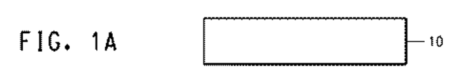
図1は、側面図で示される方法フロー図であり、従来の方法と材料による半導体素子の製造を説明する。 FIG. 1 is a method flow diagram shown in a side view, illustrating the manufacture of semiconductor devices using conventional methods and materials.
図1Aでは、p型シリコン基板10が提供される。基板は、単結晶シリコンで構成しても、多結晶シリコンで構成してもよい。図1Bに示されるように、図1Bのn型層20が形成されて、p−n接合が作られる。n型層を形成するために用いられる方法は一般に、周期表V族に属するドナードーパント、好ましくはリン(P)を、三塩化リン(POCl3)を用いて熱拡散させることによる。拡散層の深さは一般に、約0.3から0.5マイクロメートル(μm)である。リンのドーピングによって、シリコンの表面抵抗は、数十オーム・パー・スクエア(Ω/□)から100オーム・パー・スクエア(Ω/□)未満程度の間まで低下する。特に何の改変も加えなければ、拡散層20は、シリコン基板10の表面全体に形成される。
In FIG. 1A, a p-
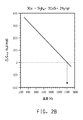
次に、この拡散層の一方の表面はレジストまたはその他によって保護され、エッチングによって、拡散層20が図1Bの成形物の1つの表面以外のすべてから除去される。レジストが除去されると、図1Cの成形物が残る。
Next, one surface of the diffusion layer is protected by resist or the like, and the
次に、図1Dに示されるように、上記のn型拡散層の上に、絶縁のための窒化シリコンSi3N4膜または窒化シリコンSiNx:H膜が形成されて、反射防止コーティング(ARC)が形成される。Si3N4またはSiNx:H反射防止コーティング30の厚さは、約700から900Åである。窒化シリコンの代替物として、酸化シリコンを反射防止コーティングとして使用してもよい。
Next, as shown in FIG. 1D, a silicon nitride Si 3 N 4 film or a silicon nitride SiNx: H film for insulation is formed on the n-type diffusion layer, and an antireflection coating (ARC) is formed. Is formed. The thickness of the Si 3 N 4 or SiNx: H
図1Eに示されるように、窒化シリコン膜30の上に表面電極用の銀ペースト50がスクリーン印刷され、その後、乾燥される。これに加えて、基板の裏面には、アルミニウムペースト60と裏面用の銀または銀/アルミニウムペースト70がスクリーン印刷され、続いて乾燥される。その後、表面および裏面ペーストの共焼成(co−firing)が、赤外炉において、約700℃から975℃の温度範囲の空気中で数分間から数十分間にわたって実行される。
As shown in FIG. 1E, a
図1Fに示されるように、焼成中、アルミニウムペーストからアルミニウムがドーパントとしてシリコン基板10の中に拡散し、高濃度のアルミニウムドーパントを含むp+層40を形成する。この層は一般に、裏面電界層(BSF)と呼ばれ、太陽電池のエネルギー変換効率を改善するのに役立つ。
As shown in FIG. 1F, during firing, aluminum diffuses from the aluminum paste as a dopant into the
焼成により、アルミニウムペースト60はアルミニウム裏面電極61にも変化する。裏面用の銀または銀/アルミニウムペースト70が同時に焼成され、銀または銀/アルミニウムの裏面電極71となる。焼成中、裏面のアルミニウムと裏面の銀または銀/アルミニウムとの間の境界が合金状態となり、それによって電気接続が確立される。アルミニウム電極はまた、シリコンをドーピングして、p+層40を形成する。アルミニウム電極へのはんだ付けは不可能であることから、裏面の一部に、銅リボンまたはその他によって太陽電池同士を相互接続するための電極として、銀の裏面タブ電極が形成される。
By baking, the
共焼成中、表面電極形成用の銀ペースト50が焼結して窒化シリコン層30を貫通し、それによって、n型層20と電気的に接触することが可能となる。このようなタイプの方法は一般に、窒化シリコンの「ファイヤスルー」または「エッチング」と呼ばれる。このファイヤスルー状態は、図1Fの層51に見られる。
During the co-firing, the surface electrode forming
従来の表面電極用の銀ペーストは、銀粉末、有機バインダ、溶媒、ガラスフリットを含有し、各種の添加剤を含んでいてもよい。銀粉末は主な電極接点材料としての役割を果たし、低い抵抗を提供する。ガラスフリットは鉛またはその他の低融点成分を含んで、軟化点を約300から600℃とするようになっていてもよい。ガラスフリットはまた、焼結された銀をシリコンに接着させる。添加剤は、n型の導電性を変化させるための追加のドーパントとして使用されてもよい。焼成中、ガラスは溶融して窒化シリコン層を貫通し、銀がn型シリコン層と電気的に接触する。焼成後の界面構造は複数の相、すなわち基板シリコン、銀−シリコンアイランド、絶縁ガラス層内の銀凝結物および、バルク焼結銀からなる。その結果、接点メカニズムは、銀−シリコンアイランドと銀凝結物によるオーム接触と薄いガラス層内のトンネリングが複合されたものである。太陽電池への電極接点は、電池の性能にとって重要である。高抵抗のシリコン/電極接点界面は、電池から外部電極への電流の伝送を妨害し、したがって、効率を低下させるであろう。したがって、電池の効率を最大限にするために、導電性ペーストの組成物と焼成プロファイルが最適化される。しかしながら、金属−シリコン界面にガラスが存在すると、接触抵抗は不可避的に、シリコンとの純金属の接触によって実現されるものより高くなる。 A conventional silver paste for a surface electrode contains silver powder, an organic binder, a solvent, glass frit, and may contain various additives. Silver powder serves as the main electrode contact material and provides low resistance. The glass frit may contain lead or other low melting point components so that the softening point is about 300 to 600 ° C. The glass frit also bonds the sintered silver to the silicon. Additives may be used as additional dopants to change n-type conductivity. During firing, the glass melts and penetrates the silicon nitride layer, and silver is in electrical contact with the n-type silicon layer. The interface structure after firing consists of a plurality of phases: substrate silicon, silver-silicon island, silver condensate in the insulating glass layer, and bulk sintered silver. As a result, the contact mechanism is a combination of ohmic contact with silver-silicon islands and silver aggregates and tunneling in a thin glass layer. The electrode contacts to the solar cell are important for battery performance. The high resistance silicon / electrode contact interface will interfere with current transfer from the battery to the external electrode and thus reduce efficiency. Therefore, the conductive paste composition and firing profile are optimized to maximize battery efficiency. However, when glass is present at the metal-silicon interface, the contact resistance is inevitably higher than that achieved by pure metal contact with silicon.
低抵抗の接点をバイポーラシリコン素子に形成することには、問題が伴う。基本的な半導体接点には必ず電位障壁があり、これによって接点は整流作用を有することになる。ショットキ障壁高さ(SBH)は、金属−半導体(MS)接合を通じて電気を伝導するための整流障壁であり、したがって、どの半導体素子にとっても、優れた動作のために非常に重要である。SBHの大きさは、半導体の多数キャリア伝導帯端のエネルギー位置とMS界面を通じた金属のフェルミ準位との不一致を反映する。金属/n型半導体界面では、SBHは伝導帯最小値とフェルミ準位の差である。SBHが低いほど、シリコンとの接点は良好である。n型シリコンとのショットキ障壁高さの低い接点を有する半導体素子が知られている。たとえば、米国特許第3,381,182号明細書、第3,968,272号明細書および第4,394,673号明細書は、金属をシリコンと接触させて配置し、加熱すると、バイポーラシリコン素子にSBHの低い接点を形成する各種のシリサイドを開示している。Borlandらの米国仮特許出願第61/088,504号明細書は、何らかの金属シリサイドの形成が起こる可能性のある窒化シリコンと周期表4Bおよび5B族に属する金属との反応によって形成される金属窒化物を、ショットキ障壁高さの低い接点として使用することを開示している。シリコン太陽電池との表面電極接点のための、n型シリコンとのガラスを含まない純粋なシリサイドの接点は開示されていない。 There are problems associated with forming low resistance contacts in bipolar silicon devices. Basic semiconductor contacts always have a potential barrier, which causes the contacts to rectify. The Schottky barrier height (SBH) is a rectifying barrier for conducting electricity through a metal-semiconductor (MS) junction and is therefore very important for good operation for any semiconductor device. The magnitude of SBH reflects the mismatch between the energy position of the majority carrier conduction band edge of the semiconductor and the Fermi level of the metal through the MS interface. At the metal / n-type semiconductor interface, SBH is the difference between the conduction band minimum and the Fermi level. The lower the SBH, the better the contact with silicon. A semiconductor device having a contact point with a low Schottky barrier height with n-type silicon is known. For example, U.S. Pat. Nos. 3,381,182, 3,968,272, and 4,394,673 disclose that bipolar silicon is placed when metal is placed in contact with silicon and heated. Various silicides are disclosed that form low SBH contacts in the device. Borland et al., US Provisional Patent Application No. 61 / 088,504, describes metal nitridation formed by the reaction of silicon nitride with the potential for some metal silicide formation with metals belonging to Periodic Tables 4B and 5B. The use of the object as a contact with a low Schottky barrier height. No pure silicide contact with n-type silicon for surface electrode contact with silicon solar cells is disclosed.
接触抵抗を大幅に減少させ、良好な接着状態を維持し、安全、安価かつ入手が容易な材料と方法を使用する、光起電力素子の表面電極接点を形成するための新規な組成物と方法が求められている。 NOVEL COMPOSITIONS AND METHODS FOR FORMING SURFACE ELECTRODE CONTACTS FOR PHOTOVOLTAIC ELEMENTS USING MATERIALS AND METHODS WHICH REDUCES ACTIVATELY, MAINTAINS GOOD AGING, AND USES SAFE, LOW PRICE AND ACCESS Is required.
光起電力素子の製造方法が開示され、この方法において、p型ベースとn型シリコン層を有するシリコン基板が提供される。窒化シリコン層が、シリコン基板のn型シリコン層の上に形成される。交換金属が窒化シリコン層と接触させて配置され、非交換金属が交換金属と接触させて配置される。シリコン基板、窒化シリコン層、交換金属および非常交換金属は焼成されて、n型シリコン層との金属シリサイド接点と、金属シリサイド接点と接触する導電性金属電極が形成される。交換金属は、コバルト、ニッケル、鉄、マンガンおよびモリブデンの群からの1つまたは複数の金属およびこれらの組み合わせであってもよい。非交換金属は好ましくは、銀、銅、錫、ビスマス、鉛、アンチモン、亜鉛、インジウム、金、カドミウム、ベリリウム、およびそれらの組み合わせの群からのものである。金属シリサイドの接点は、n型シリコン層とのショットキ障壁高さの低い接点となる。光起電力素子は、この方法により、このような金属シリサイド接点を有するように作製することができる。 A method of manufacturing a photovoltaic device is disclosed in which a silicon substrate having a p-type base and an n-type silicon layer is provided. A silicon nitride layer is formed on the n-type silicon layer of the silicon substrate. An exchange metal is placed in contact with the silicon nitride layer and a non-exchange metal is placed in contact with the exchange metal. The silicon substrate, silicon nitride layer, exchange metal and emergency exchange metal are fired to form a metal silicide contact with the n-type silicon layer and a conductive metal electrode in contact with the metal silicide contact. The exchange metal may be one or more metals from the group of cobalt, nickel, iron, manganese and molybdenum and combinations thereof. The non-exchange metal is preferably from the group of silver, copper, tin, bismuth, lead, antimony, zinc, indium, gold, cadmium, beryllium, and combinations thereof. The contact point of the metal silicide is a contact point with a low Schottky barrier height with the n-type silicon layer. Photovoltaic elements can be made with this method to have such metal silicide contacts.
1つの実施形態において、シリコン基板のn型シリコン層の上の窒化シリコン層と接触して配置された交換金属と、交換金属と接触して配置された非交換金属はどちらも、フラックスで被覆される。開示される別の実施形態において、交換金属と非交換金属が組み合わされて金属組成物が形成され、その後、この金属組成物がシリコン基板のn型シリコン層の上に堆積される。交換金属は好ましくは、平均直径が以下の直径、すなわち0.2、0.5、1、3、5および10マイクロメートルのうちのいずれか2つの値の間で、かつそれら2つの値を含む粒子の形態である。非交換金属は好ましくは、平均直径が以下の直径、0.2、0.5、1、3、5および10マイクロメートルのうちのいずれか2つの値の間で、かつそれら2つの値を含む粒子の形態である。 In one embodiment, both the exchange metal placed in contact with the silicon nitride layer over the n-type silicon layer of the silicon substrate and the non-exchange metal placed in contact with the exchange metal are coated with a flux. The In another disclosed embodiment, exchange metal and non-exchange metal are combined to form a metal composition, which is then deposited on an n-type silicon layer of a silicon substrate. The exchange metal preferably has an average diameter between the following two values: 0.2, 0.5, 1, 3, 5, and 10 micrometers, and includes these two values The form of the particles. The non-exchange metal preferably has an average diameter between the following two values of 0.2, 0.5, 1, 3, 5 and 10 micrometers and includes these two values The form of the particles.
開示される1つの実施形態において、金属組成物の交換金属と非交換金属は、交換金属と非交換金属の合金の形態であり、この合金は好ましくは、平均直径が以下の直径、すなわち0.2、0.5、1、3、5および10マイクロメートルのうちのいずれか2つの値の間で、かつそれら2つの値を含む合金粒子の形態であってもよい。好ましくは、交換金属は、金属組成物の金属総量の1から40重量パーセントを構成する。開示される1つの実施形態において、合金金属粒子はフラックスで被覆される。 In one disclosed embodiment, the exchange metal and non-exchange metal of the metal composition are in the form of an alloy of exchange metal and non-exchange metal, which alloy preferably has an average diameter of It may be in the form of alloy particles between and including any two values of 2, 0.5, 1, 3, 5, and 10 micrometers. Preferably, the exchange metal comprises 1 to 40 weight percent of the total metal of the metal composition. In one disclosed embodiment, the alloy metal particles are coated with a flux.
開示される1つの実施形態において、シリコン基板、窒化シリコン層、交換金属および非交換金属は、400℃から950℃の温度で焼成される。1つの実施形態において、シリコン基板、窒化シリコン層および交換金属は、酸素分圧が10-6気圧以下の低酸素雰囲気中で焼成される。高窒素雰囲気中の焼成も開示される。別の実施形態では、交換金属と非交換金属は、フラックスで被覆され、400℃から950℃の温度の空気雰囲気中で焼成される。 In one disclosed embodiment, the silicon substrate, silicon nitride layer, exchange metal and non-exchange metal are fired at a temperature of 400 ° C. to 950 ° C. In one embodiment, the silicon substrate, the silicon nitride layer and the exchange metal are fired in a low oxygen atmosphere having an oxygen partial pressure of 10 −6 atm or less. Firing in a high nitrogen atmosphere is also disclosed. In another embodiment, the exchange metal and non-exchange metal are coated with a flux and fired in an air atmosphere at a temperature of 400 to 950 ° C.
シリコン太陽電池の製造方法もまた開示される。開示される方法によれば、p型シリコンベースとn型シリコン層を有するシリコン基板が提供され、シリコン基板のn型シリコン層の上に窒化シリコン反射防止層が形成され、前記窒化シリコン反射防止層と接触させて交換金属が配置され、交換金属と接触させて非交換金属が配置され、シリコン基板、窒化シリコン層、交換金属および非交換金属が焼成されて、n型シリコン層との金属シリサイド接点と、金属シリサイド接点と接触する導電性金属電極が形成される。交換金属と非交換金属は、薄膜堆積によって、窒化シリコン反射防止層と接触させて配置されてもよい。あるいは、交換金属と非交換金属は、厚膜堆積によって、窒化シリコン反射防止層と接触するにように配置されてもよい。反射防止コーティングの厚さは好ましくは、70から100ナノメートルの範囲である。開示される交換金属は、ニッケル、コバルト、鉄、マンガン、モリブデンおよびそれらの組み合わせを含む。開示される非交換金属は、銀、銅、錫、ビスマス、鉛、アンチモン、ヒ素、亜鉛、金、カドミウム、ベリリウムおよびそれらの組み合わせを含む。 A method of manufacturing a silicon solar cell is also disclosed. According to the disclosed method, a silicon substrate having a p-type silicon base and an n-type silicon layer is provided, a silicon nitride antireflection layer is formed on the n-type silicon layer of the silicon substrate, and the silicon nitride antireflection layer is provided. The exchange metal is placed in contact with the non-exchange metal, the non-exchange metal is placed in contact with the exchange metal, the silicon substrate, the silicon nitride layer, the exchange metal and the non-exchange metal are fired, and the metal silicide contact with the n-type silicon layer A conductive metal electrode in contact with the metal silicide contact is formed. The exchange metal and non-exchange metal may be placed in contact with the silicon nitride antireflection layer by thin film deposition. Alternatively, the exchange metal and non-exchange metal may be placed in contact with the silicon nitride antireflective layer by thick film deposition. The thickness of the antireflective coating is preferably in the range of 70 to 100 nanometers. The disclosed exchange metals include nickel, cobalt, iron, manganese, molybdenum and combinations thereof. Non-exchangeable metals disclosed include silver, copper, tin, bismuth, lead, antimony, arsenic, zinc, gold, cadmium, beryllium and combinations thereof.
光電池の窒化シリコン反射防止層の上に電気接点を生成するための厚膜組成物もまた開示される。厚膜組成物は、ニッケル、コバルト、鉄、マンガン、モリブデンおよびこれらの組み合わせの群から選択される1つまたは複数の交換金属と、銀、銅、錫、ビスマス、鉛、アンチモン、ヒ素、亜鉛、金、カドミウムとベリリウムおよびこれらの組み合わせから選択される1つまたは複数の非交換金属を含む。交換金属と非交換金属は有機媒体中で提供され、交換金属と非常交換金属は平均直径が0.2から10マイクロメートルの範囲の粒子の形態である。1つの好ましい実施形態において、交換金属と非交換金属は合金化され、そのような合金の粒子の形態である。金属合金粒子は、フラックスで被覆されてもよい。また、開示されるこの組成物から形成される表面電極接点を有するシリコン太陽電池も開示される。 A thick film composition for generating electrical contacts on the silicon nitride antireflective layer of a photovoltaic cell is also disclosed. The thick film composition comprises one or more exchange metals selected from the group of nickel, cobalt, iron, manganese, molybdenum and combinations thereof, and silver, copper, tin, bismuth, lead, antimony, arsenic, zinc, Including one or more non-exchange metals selected from gold, cadmium and beryllium, and combinations thereof. Exchange and non-exchange metals are provided in an organic medium, and exchange and emergency exchange metals are in the form of particles having an average diameter ranging from 0.2 to 10 micrometers. In one preferred embodiment, the exchange metal and non-exchange metal are alloyed and are in the form of particles of such an alloy. The metal alloy particles may be coated with a flux. Also disclosed are silicon solar cells having surface electrode contacts formed from the disclosed composition.
n型シリコン層を有する基板と、n型シリコン層の上に堆積され、これに接着される金属シリサイド接点であって、金属がニッケル、コバルト、鉄、マンガン、モリブデンおよびそれらの組み合わせである金属シリサイド接点と、前記金属シリサイドに接着され、その上に堆積される導電性金属電極と、を含む光起電力素子であって、導電性金属電極が、銀、銅、錫、ビスマス、鉛、アンチモン、ヒ素、亜鉛、ゲルマニウム、金、カドミウム、ベリリウム、およびそれらの組み合わせから選択される導電性金属から構成される光起電力素子もまた開示される。 A substrate having an n-type silicon layer and a metal silicide contact deposited on and adhered to the n-type silicon layer, wherein the metal is nickel, cobalt, iron, manganese, molybdenum and combinations thereof A photovoltaic device comprising: a contact; and a conductive metal electrode adhered to and deposited on the metal silicide, wherein the conductive metal electrode is silver, copper, tin, bismuth, lead, antimony, Also disclosed is a photovoltaic device comprised of a conductive metal selected from arsenic, zinc, germanium, gold, cadmium, beryllium, and combinations thereof.
図1に示される参照番号を以下に説明する。
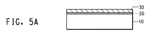
10:p型シリコン基板
20:n型拡散層
30:反射防止コーティング
40:p+層(裏面電界層、BSF)
50:表面に形成された銀ペースト
51:銀表面電極(表面の銀ペーストの焼成により得られる)
60:裏面に形成されたアルミニウムペースト
61:アルミニウム裏面電極(裏面のアルミニウムペーストの焼成により得られる)
70:裏面に形成された銀または銀/アルミニウムペースト
71:銀または銀/アルミニウム裏面電極(裏面の銀ペーストの焼成により得られる)
Reference numerals shown in FIG. 1 will be described below.
10: p-type silicon substrate 20: n-type diffusion layer 30: antireflection coating 40: p + layer (back surface field layer, BSF)
50: Silver paste formed on the surface 51: Silver surface electrode (obtained by firing the silver paste on the surface)
60: Aluminum paste formed on the back surface 61: Aluminum back electrode (obtained by baking the aluminum paste on the back surface)
70: Silver or silver / aluminum paste formed on the back surface 71: Silver or silver / aluminum back electrode (obtained by firing the silver paste on the back surface)
一般的な慣行により、以下に説明する図面の各種の特徴は、必ずしも正しい縮尺で描かれていない。図中の各種の特徴と要素の寸法は、本発明の実施形態をより明快に示すために、拡大または縮小されているかもしれない。 In accordance with common practice, the various features of the drawings described below are not necessarily drawn to scale. Various features and element dimensions in the figures may be scaled up or down to more clearly illustrate embodiments of the present invention.
n型シリコンとのショットキ障壁高さの低い電極接点を有する光起電力素子が開示される。また、n型シリコンとのショットキ障壁高さの低い電極接点を有する光起電力素子の製造方法も開示される。開示される光起電力素子は太陽電池であるが、これらはまた、光検出器や発光ダイオード等、n型シリコンとの電極接点を有するその他の光起電力素子であってもよい。開示される実施形態は、シリサイドから構成されるショットキ障壁高さの低い電極接点を有するn型シリコン上の表面電極を備える太陽電池である。 A photovoltaic device having electrode contacts with low Schottky barrier height with n-type silicon is disclosed. Also disclosed is a method for manufacturing a photovoltaic device having an electrode contact with n-type silicon and a low Schottky barrier height. Although the disclosed photovoltaic elements are solar cells, they may also be other photovoltaic elements having electrode contacts with n-type silicon, such as photodetectors and light emitting diodes. The disclosed embodiment is a solar cell comprising a surface electrode on n-type silicon having a low Schottky barrier electrode contact made of silicide.
本明細書において、「交換金属」(M)という用語は、窒化シリコンと反応して、安定した高電導性金属と窒素ガスを生成し、金属窒化物を形成しない金属または金属の混合物を意味する。たとえば、交換金属は、以下の反応式によって窒化シリコンと反応する。
3M+Si3N4→3MSi+2N2(気体)
As used herein, the term “exchange metal” (M) refers to a metal or mixture of metals that reacts with silicon nitride to produce a stable, highly conductive metal and nitrogen gas that does not form a metal nitride. . For example, exchange metal reacts with silicon nitride according to the following reaction equation.
3M + Si 3 N 4 → 3MSi + 2N 2 (gas)
このような金属には、ニッケル(Ni)、コバルト(Co)、モリブデン(Mo)、マンガン(Mn)および鉄(Fe)の群からの金属またはその混合物が含まれる。これらの金属は、この反応を可能にする熱力学的特性を有する。 Such metals include metals from the group of nickel (Ni), cobalt (Co), molybdenum (Mo), manganese (Mn) and iron (Fe) or mixtures thereof. These metals have thermodynamic properties that allow this reaction.
MSiは、好ましいシリサイドが得られるものとして広く示されているが、存在する金属の量と反応の程度に応じて、その他の金属シリサイドを形成してもよい。このような金属シリサイドはMxSiyと表してもよく、Mは上記の群からの金属、Siはシリコン、xとyは金属含有量と反応の程度に応じて変化しうる。組成物には、Ni3Si、Ni5Si、Ni2Si、Ni3Si2、NiSi、Co3Si、Co2Si、CoSi、Mn3Si、Mn5Si3、MnSi、Mo3Si、Mo3Si2、Fe3Si、Fe5Si3およびFeSiが含まれるが、これらに限定されない。組成物が完全な化学量論的組成でないこともある。 MSi has been widely shown to provide a preferred silicide, but other metal silicides may be formed depending on the amount of metal present and the extent of reaction. Such a metal silicide may be expressed as M x Si y , where M is a metal from the above group, Si is silicon, and x and y may vary depending on the metal content and the extent of reaction. The compositions include Ni 3 Si, Ni 5 Si, Ni 2 Si, Ni 3 Si 2 , NiSi, Co 3 Si, Co 2 Si, CoSi, Mn 3 Si, Mn 5 Si 3 , MnSi, Mo 3 Si, Mo 3 Si 2 , Fe 3 Si, Fe 5 Si 3 and FeSi are included, but are not limited to these. The composition may not be a complete stoichiometric composition.
本明細書において、「非交換金属」という用語は、窒化シリコンの窒素と交換して導電性金属シリサイドを生成しえない、すなわち窒化シリコンに対して不活性の金属または金属の混合物を意味する。好ましい非交換金属は、融点が比較的低く、交換金属と混合または合金化すると、反応温度を下げることができ、反応速度を加速させることができる。金属組成物は、共晶組成の利用によって所望の融点とするために、複数の要素を用いて設計してもよい。 As used herein, the term “non-exchange metal” refers to a metal or mixture of metals that cannot exchange with nitrogen in silicon nitride to produce a conductive metal silicide, ie, inert to silicon nitride. Preferred non-exchange metals have a relatively low melting point, and when mixed or alloyed with exchange metals, the reaction temperature can be lowered and the reaction rate can be accelerated. The metal composition may be designed using a plurality of elements in order to achieve a desired melting point by utilizing a eutectic composition.
非交換金属はまた、電流通過特性のために、電気抵抗を比較的低くするように選択される。非交換金属は、銀(Ag)、銅(Cu)、錫(Sn)、ビスマス(Bi)、鉛(Pb)、ヒ素(As)、アンチモン(Sb)、亜鉛(Zn)、金(Au)、カドミウム(Cd)およびベリリウム(Be)等の金属の群から選択されてもよいが、これらに限定されない。高い融点を有するものなど、たとえばパラジウム(Pd)等のその他の金属を少量だけ含めて、その他の特定の特性を持たせるようにしてもよい。5A族の元素(リン、ヒ素、アンチモン、ビスマス)を少量含めてもよく、それは、これらが上記に加えてドナードーパントとしても機能するかもしれないからである。非交換金属のグルーブは一般に、周期表3族の元素(ボロン(B)、アルミニウム(Al)、ガリウム(Ga)、インジウム(In)およびタリウム(Tl))を含まず、それは、これらがn型シリコン中でアクセプタドーパントとして機能し、その表面抵抗が高くなりすぎるからである。 Non-exchange metal is also selected to have a relatively low electrical resistance due to the current passing characteristics. Non-exchange metals are silver (Ag), copper (Cu), tin (Sn), bismuth (Bi), lead (Pb), arsenic (As), antimony (Sb), zinc (Zn), gold (Au), It may be selected from the group of metals such as, but not limited to, cadmium (Cd) and beryllium (Be). Other metals such as those having a high melting point, such as palladium (Pd), may be included to provide other specific characteristics. A small amount of Group 5A elements (phosphorus, arsenic, antimony, bismuth) may be included because they may function as donor dopants in addition to the above. Non-exchange metal grooves generally do not contain elements of Group 3 of the periodic table (boron (B), aluminum (Al), gallium (Ga), indium (In) and thallium (Tl)), which are n-type This is because it functions as an acceptor dopant in silicon and its surface resistance becomes too high.
図2の計算値のグラフは、窒素分圧が1気圧のときの窒化シリコンと各種交換金属との自由エネルギー(ΔG)対温度を示す。金属と窒化シリコンの反応開始温度は、デルタG、すなわち反応の自由エネルギーがゼロの地点と予測できる。このようにして、1気圧の窒素流雰囲気下では、ニッケルは約1250°Kを超える温度でなければ窒化シリコンと反応しないことが予測される。コバルト、モリブデン、マンガンおよび鉄に関しては、反応温度はそれぞれ、約1400°K、1150°K、1650°Kおよび1600°Kである。これらの温度は一般に、シリコン太陽電池の加工には高すぎる。しかしながら、交換金属を融点の低い金属と合金化することにより、反応温度を低くすることができる。 The graph of calculated values in FIG. 2 shows the free energy (ΔG) vs. temperature of silicon nitride and various exchange metals when the nitrogen partial pressure is 1 atm. The reaction start temperature between the metal and silicon nitride can be predicted as delta G, that is, the point where the free energy of reaction is zero. In this way, it is expected that nickel will not react with silicon nitride unless the temperature exceeds about 1250 ° K. under a 1 atmosphere nitrogen flow atmosphere. For cobalt, molybdenum, manganese and iron, the reaction temperatures are about 1400 ° K, 1150 ° K, 1650 ° K and 1600 ° K, respectively. These temperatures are generally too high for processing silicon solar cells. However, the reaction temperature can be lowered by alloying the exchange metal with a metal having a low melting point.
図3は、窒素の分圧を下げることによってニッケルの反応温度がどのように下がるかを示す概念的グラフである。その他の金属も計算値は同様である。したがって、反応温度を下げる1つの方法は、窒素の分圧を下げることである。これは、窒素を、たとえばアルゴン等の中性の気体で希釈することによって実現してもよい。その他の気体、たとえば一酸化炭素または水素も希釈剤として利用してもよい。 FIG. 3 is a conceptual graph showing how the reaction temperature of nickel is lowered by lowering the partial pressure of nitrogen. The calculation values of other metals are the same. Thus, one way to lower the reaction temperature is to reduce the partial pressure of nitrogen. This may be achieved by diluting nitrogen with a neutral gas such as argon. Other gases such as carbon monoxide or hydrogen may also be utilized as diluents.
ニッケルシリサイドとコバルトシリサイドは、n型シリコンとの接点のショットキ障壁高さが、図4に示されるように(“Barrier Heights to n−Silicon”,Andrews et al.,J.Vac.Sci.Tech 11,6,972,1974から引用)、0.6から0.65eV(電子ボルト)のオーダである。これは、シリコン太陽電池のn型シリコンに用いられる従来の接点である金属銀(evは約0.65eV)と近い。したがって、ニッケルおよびコバルトシリサイドはn型シリコンとの接触抵抗の低い接点として好適な選択肢である。本明細書において、n型シリコンとの「ショットキ障壁高さの低い」接点は、接触抵抗が0.8eV未満である。 Nickel silicide and cobalt silicide Schottky barrier height of the contact point between the n-type silicon, as shown in FIG. 4 ( "Barrier Heights to n- Silicon", Andrews et al., J.Vac.Sci.Tech 11 , 6, 972, 1974), 0.6 to 0.65 eV (electron volt). This is close to metal silver (ev is about 0.65 eV), which is a conventional contact used for n-type silicon of silicon solar cells. Therefore, nickel and cobalt silicide are suitable choices as a contact having low contact resistance with n-type silicon. In this specification, a contact with a “low Schottky barrier height” contact with n-type silicon has a contact resistance of less than 0.8 eV.
上記の金属は、薄膜プロセスによって窒化シリコン上に堆積されてもよく、このプロセスにはスパッタリング、金属蒸着、化学気相成長法、原子層堆積法、パルスレーザ堆積法およびその他が含まれるが、これらに限定されない。交換金属と非交換金属は、その基本的な状態で、または個別の層で堆積されても、または共堆積によって混合物または合金を形成してもよい。薄膜法によって堆積される金属は一般に、所望のパターンを画成するためのマスクまたはフォトレジストを介して、窒化シリコンの表面上に薄い、連続する層として堆積される。 The above metals may be deposited on silicon nitride by a thin film process, which includes sputtering, metal evaporation, chemical vapor deposition, atomic layer deposition, pulsed laser deposition, and others. It is not limited to. Exchange and non-exchange metals may be deposited in their basic state, in separate layers, or may form a mixture or alloy by co-deposition. Metals deposited by thin film methods are typically deposited as a thin, continuous layer on the surface of silicon nitride through a mask or photoresist to define the desired pattern.
金属はまた、厚膜プロセスで堆積されてもよい。厚膜プロセスにはスクリーン印刷、インクジェット印刷またはフォトイメージング法が含まれるが、これらに限定されない。スクリーン印刷は、費用対効果の高いプロセスであるため、有利である。この場合、前述の交換金属と非交換金属を粉末の形態で含むペーストが、スクリーンを介して窒化シリコンの表面上に印刷される。スクリーンが、所望のパターンを画定する。 The metal may also be deposited in a thick film process. Thick film processes include, but are not limited to, screen printing, ink jet printing, or photo imaging methods. Screen printing is advantageous because it is a cost-effective process. In this case, a paste containing the aforementioned exchange metal and non-exchange metal in the form of powder is printed on the surface of silicon nitride via a screen. A screen defines the desired pattern.
交換金属から作製される厚膜ペーストのスクリーン印刷に使用するものとして適した粉末は、できるだけ酸化物を含まず、上記の反応が交換金属の自然酸化物によって妨害されないようにするべきである。交換金属の場合、その酸化特性により、室温の空気中で酸化物が所定の厚さに形成されるため、粉末の粒子の大きさが大きいほど、酸化物の総含有量は低くなる。したがって、酸化物のレベルをなるべく低くするためには、一般に、良好な厚膜ペースト形成特性と矛盾しない最大の粒子サイズの粉末を使用することが好ましい。最適な厚膜ペースト特性のためには、このような交換金属粉末の平均直径は、以下の直径、すなわち0.2、0.5、1、3、5および10マイクロメートルのうちのいずれか2つの値の間で、かつそれら2つの値を含むものであるべきであり、より好ましくは0.5〜5マイクロメートルである。非交換金属から作製される適当な粉末もまた、できるだけ酸化物を含まないものであるべきである。非交換金属粉末の平均直径は、以下の直径、すなわち0.2、0.5、1、3、5および10マイクロメートルのうちのいずれか2つの値の間で、かつそれら2つの値を含むものであり、好ましくは0.5から5マイクロメートルの間であるべきである。 Powders suitable for use in the screen printing of thick film pastes made from exchange metals should be as free of oxides as possible so that the above reactions are not disturbed by the native oxides of the exchange metals. In the case of an exchange metal, an oxide is formed in a predetermined thickness in air at room temperature due to its oxidation characteristics. Therefore, the larger the particle size of the powder, the lower the total oxide content. Therefore, in order to keep the oxide level as low as possible, it is generally preferable to use a powder with the largest particle size consistent with good thick film paste formation characteristics. For optimal thick film paste properties, the average diameter of such exchange metal powders is any of the following diameters: 0.2, 0.5, 1, 3, 5, and 10 micrometers. It should be between two values and include those two values, more preferably 0.5-5 micrometers. Suitable powders made from non-exchange metals should also be as free of oxides as possible. The average diameter of the non-exchange metal powder is between and including any two values of the following diameters: 0.2, 0.5, 1, 3, 5 and 10 micrometers And preferably should be between 0.5 and 5 micrometers.
厚膜堆積の場合、前述の金属粉末は、機械的混合によって有機媒体と混合され、印刷に適した濃度とレオロジを有する、「厚膜ペースト」と呼ばれる粘性組成物を形成する。有機媒体は、焼成プロセスの初期段階で消散するという点で、一時的な材料である。有機材料が完全に消散する温度は、厚膜ペースト組成物の中の有機材料の化学的性質と量によって異なるため、組成物は、消散がより低い温度で起こるようにも、より高い温度で起こるようにも設計できる。有機媒体は、金属粉末が十分な安定度でその中に分散できるようなものでなければならない。媒体のレオロジ特性は、組成物に良好な塗布特性、たとえば金属粉末の安定した分散、スクリーン印刷またはその他の所望の塗布プロセスに適した粘度とチクソ性、物質の適当なペースト湿潤性および良好な乾燥速度を持たせるものでなければならない。開示される厚膜組成物で使用される有機媒体は好ましくは、非水性の不活性薬品である。各種の有機媒体のいずれでも使用でき、増粘剤、安定剤および/またはその他の一般的な添加剤が含まれていても、含まれていなくてもよい。有機媒体は一般に、溶媒中の高分子溶液である。これに加えて、界面活性剤等の添加剤を少量、有機媒体に含めてもよい。 For thick film deposition, the aforementioned metal powder is mixed with an organic medium by mechanical mixing to form a viscous composition called “thick film paste” having a concentration and rheology suitable for printing. The organic medium is a temporary material in that it dissipates early in the firing process. Because the temperature at which the organic material completely dissipates depends on the chemistry and amount of organic material in the thick film paste composition, the composition occurs at a higher temperature, even though the dissipation occurs at a lower temperature Can also be designed. The organic medium must be such that the metal powder can be dispersed therein with sufficient stability. The rheological properties of the media indicate that the composition has good application properties such as stable dispersion of metal powder, viscosity and thixotropy suitable for screen printing or other desired application processes, appropriate paste wettability of the material and good drying. Must be speedy. The organic medium used in the disclosed thick film composition is preferably a non-aqueous inert chemical. Any of a variety of organic media can be used and may or may not contain thickeners, stabilizers and / or other common additives. The organic medium is generally a polymer solution in a solvent. In addition, a small amount of an additive such as a surfactant may be included in the organic medium.
最もよく使用される有機媒体の高分子化合物は、エチルセルロースである。有機媒体用として有益なその他の高分子化合物には、エチルヒドロキシエチルセルロース、ウッドロジン、エチルセルロースとフェノール樹脂の混合物、より低アルコールのポリメタクリレートおよび、エチレングリコールモノブチルエーテルモノアセテートがある。 The most commonly used organic medium polymer is ethyl cellulose. Other polymeric compounds useful for organic media include ethyl hydroxyethyl cellulose, wood rosin, mixtures of ethyl cellulose and phenolic resins, lower alcohol polymethacrylates, and ethylene glycol monobutyl ether monoacetate.
開示される厚膜組成物に見られる、最も広く使用される溶媒は、エステルアルコールと、アルファまたはベータテルピネオール等のテルペンまたはそれらと、ケロシン、ジブチルフタレート、ブチルカルビトール、ブチルカルビトールアセテート、ヘキシレングリコールおよび高沸点アルコール及びアルコールエステル等のその他の溶媒との混合物である。これに加えて、基板上に塗布した後の急速硬化を促進する揮発性液体を媒剤に含めることができる。上記およびその他の溶媒の各種の組み合わせを調製して、所望の粘度と揮発特性を得る。 The most widely used solvents found in the disclosed thick film compositions are ester alcohols and terpenes such as alpha or beta terpineol or they and kerosene, dibutyl phthalate, butyl carbitol, butyl carbitol acetate, hexylene Mixtures with glycols and other solvents such as high boiling alcohols and alcohol esters. In addition, the vehicle may include a volatile liquid that promotes rapid curing after application on the substrate. Various combinations of the above and other solvents are prepared to obtain the desired viscosity and volatility characteristics.
有機媒体中に存在する高分子化合物(高分子化合物と溶媒)は、選択された高分子化合物に応じて、組成物の1重量%から11重量%の範囲である。厚膜組成物の中の有機媒体と金属成分との比は、ペーストの塗布方法と使用される有機媒体の種類によって異なり、変化しうる。通常、厚膜組成物は、金属成分を70−95重量%と、良好な湿潤性を得るために有機媒体を5−30重量%含むであろう。 The polymer compound (polymer compound and solvent) present in the organic medium ranges from 1% to 11% by weight of the composition, depending on the polymer compound selected. The ratio of the organic medium to the metal component in the thick film composition may vary depending on the paste application method and the type of organic medium used. Typically, the thick film composition will contain 70-95% by weight of the metal component and 5-30% by weight of organic medium to obtain good wettability.
ショットキ障壁高さの低い接点(窒化シリコン内の窒素と交換金属の交換によって金属シリサイドを形成することから得られる)は、窒化シリコン層と略同じ厚さ(70から100ナノメートル)であってもよく、あるいは、焼成プロセス、どれだけの交換金属が堆積されたか、および下地となるn型シリコンと反応したか否かに応じて、数マイクロメートルの大きさであってもよい。しかしながら、電流を外部回路に通過させるための、低抵抗の電流キャリアを形成することも有利である。言い換えれば、低抵抗の電極または追加の金属層が望ましい。これは、焼成プロセスの前に、交換金属層の上に非交換金属層を堆積させることによって実現してもよい。別の方法は、適当な量の交換金属と非交換金属を共堆積させることである。共堆積方式は、交換金属と非交換金属との金属混合物または合金を含んでいてもよい。混合物または合金組成物における交換金属の量は、窒化シリコンの厚さ、交換金属および堆積の厚さに合わせて調整される。一般に、交換金属は組成物内の金属の約1−40重量%を占め、非交換金属は組成物の中の金属の99−60重量%を含む。 A contact with a low Schottky barrier height (obtained from forming a metal silicide by exchanging nitrogen and exchange metal in silicon nitride) is about the same thickness (70 to 100 nanometers) as the silicon nitride layer. Alternatively, it may be a few micrometers in size, depending on the firing process, how much exchange metal has been deposited, and whether it has reacted with the underlying n-type silicon. However, it is also advantageous to form a low resistance current carrier for passing current through an external circuit. In other words, low resistance electrodes or additional metal layers are desirable. This may be achieved by depositing a non-exchange metal layer on the exchange metal layer prior to the firing process. Another method is to co-deposit appropriate amounts of exchange and non-exchange metals. Co-deposition schemes may include metal mixtures or alloys of exchange and non-exchange metals. The amount of exchange metal in the mixture or alloy composition is tailored to the thickness of the silicon nitride, exchange metal and deposition thickness. In general, the exchange metal comprises about 1-40% by weight of the metal in the composition and the non-exchange metal comprises 99-60% by weight of the metal in the composition.
本明細書で説明するショットキ障壁高さの低い電極接点を有する太陽電池は、以下の方法で製造してもよい。 A solar cell having an electrode contact with a low Schottky barrier height described in this specification may be manufactured by the following method.
図5を参照すると、図5Aに示される成形物が提供される。この成形物は、単結晶シリコンまたは多結晶シリコンを含んでもよく、p型シリコン基板10、n型拡散層20および反射防止コーティング30を有する。図5Aに示される成形物は、図1Dに示される成形物に関して前述したように準備されてもよい。
Referring to FIG. 5, the molding shown in FIG. 5A is provided. The molding may include single crystal silicon or polycrystalline silicon, and has a p-
図5を参照すると、図1Dの成形物が図5Aとして提供され、示されている。図5Bを参照すると、基板の裏面に、アルミニウムペースト60と裏面用の銀または銀/アルミニウムペースト70が連続してスクリーン印刷され、乾燥される。その後、裏面用のペーストの焼成が、赤外炉において、空気中で約700℃から975℃の温度範囲で、数分間から数十分間にわたって行われる。焼成により、図5Cの成形物が生成される。
Referring to FIG. 5, the molding of FIG. 1D is provided and shown as FIG. 5A. Referring to FIG. 5B, the
図5Cを参照すると、従来の方法のように、焼成中にアルミニウムペーストからアルミニウムがドーパントとしてシリコン基板10の中に拡散し、高濃度のアルミニウムドーパントを含むp+層40が形成される。
Referring to FIG. 5C, as in the conventional method, aluminum is diffused from the aluminum paste as a dopant into the
焼成により、アルミニウムペースト60はアルミニウム裏面電極61に変化する。裏面用の銀または銀/アルミニウムペースト70も同時に焼成されて、銀または銀/アルミニウム裏面電極71となる。焼成中、裏面のアルミニウムと裏面の銀または銀/アルミニウムの間の境界は合金状態となり、それによって電気接続が確立される。アルミニウム電極は裏面電極のほとんどの領域を占めるが、その1つの理由はp+層40を形成しなければならないからである。アルミニウム電極へのはんだ付けは不可能であるため、裏面の一部に、銅リボンまたはその他により、太陽電池同士を相互接続するための電極としての銀の裏面タブ電極が形成される。
By baking, the
ここで、本明細書に記載される新規な交換金属組成物は、厚膜堆積または薄膜堆積プロセスによって、窒化シリコン絶縁膜30の上に、図5Dの80として示される表面電極のフィンガおよび/またはバスバーに対応するパターンで塗布される。堆積は、交換金属の次に非交換金属と、同じパターン上に別々に堆積させることによっても(図5Dでは両方の層が単独の層80として示されている)、あるいは交換金属と非交換金属の混合または交換金属/非交換金属合金を1回で堆積させることによっても実現できる。
Here, the novel exchange metal compositions described herein can be applied to the surface electrode fingers and / or shown as 80 in FIG. 5D on the silicon
ここで、堆積された金属組成物を焼成する。焼成は一般に、400℃から950℃の範囲の温度の炉の中で行われ、実際の温度は金属の組成によって異なる。この範囲の中の最も低い温度で焼成することが好ましいかもしれず、これは、金属の酸化を大幅に抑制するからである。焼成は保護雰囲気内で行ってもよく、この雰囲気は真空、純窒素ガス、水素と窒素の混合物または、アルゴン等のその他の気体、一酸化炭素および/または水等の混合物であってもよい。このような気体の混合物は、焼成プロセス中に、交換金属と非交換金属の酸化を防止するために、酸素と窒素の分圧を制御するのに使用されてもよい。酸化防止に必要な正確な酸素分圧(PO2)は、金属の組成によって異なる。金属を酸化から完全に保護する雰囲気は、“F.D.Richardson and J.H.E.Jeffes,J.Iron Steel Inst.,160,261(1948)”に開示されている温度計算または図に応じて、酸化物形成の標準的自由エネルギーから熱力学的に求めることができる。しかしながら、一般には、約10-6から10-14気圧の酸素分圧(PO2)が適当である。これは一般に、純窒素、一酸化炭素/二酸化炭素混合物、アルゴン、フォーミングガス(窒素中に水素が1−4%)、水素とアルゴンの混合物、または真空を使用することによって実現できる。アルゴン等の中性の気体の使用は、これが窒素を希釈し、反応温度を下げるため、有利であるかもしれない。二酸化炭素と一酸化炭素もまた、窒素の希釈に使用してよい。さらに保護力を高めるためには、有機媒体の熱分解中に、一酸化炭素と水素を含む原位置還元性雰囲気(in−situ reducing atmosphere)を意図的に形成してもよい。より高温にならないと消散しない媒体により、これを実現してもよい。これに加えて、分解中に一酸化炭素と水素を生成するように特に設計された有機材料をペーストに添加してもよい。このような添加には、ギ酸塩、酢酸塩およびその他が含まれる。有機成分の熱分解からの原位置還元性雰囲気は、有機媒体の化学的性質と成分によって調整して、状況により、保護雰囲気を使用せずに空気中で焼成を行えるようにすることができる。チタンプレートまたはセッタ等の酸素ゲッタもまた、酸素を気体から除去するのに使用してもよく、あるいは保護フラックスを用いてもよい。 Here, the deposited metal composition is fired. Firing is generally performed in a furnace having a temperature in the range of 400 ° C. to 950 ° C., and the actual temperature depends on the metal composition. It may be preferable to fire at the lowest temperature in this range, since this significantly suppresses metal oxidation. Firing may be performed in a protective atmosphere, which may be a vacuum, pure nitrogen gas, a mixture of hydrogen and nitrogen, or another gas such as argon, a mixture of carbon monoxide and / or water. Such gaseous mixtures may be used to control the partial pressure of oxygen and nitrogen to prevent oxidation of exchanged and non-exchanged metals during the firing process. The exact oxygen partial pressure (PO 2 ) required for oxidation prevention depends on the metal composition. The atmosphere that completely protects the metal from oxidation is described in the temperature calculations or figures disclosed in “FD Richardson and JH Jeffs, J. Iron Steel Inst., 160, 261 (1948)”. Accordingly, it can be determined thermodynamically from the standard free energy of oxide formation. In general, however, an oxygen partial pressure (PO 2 ) of about 10 −6 to 10 −14 atmospheres is suitable. This can generally be achieved by using pure nitrogen, a carbon monoxide / carbon dioxide mixture, argon, forming gas (1-4% hydrogen in nitrogen), a mixture of hydrogen and argon, or a vacuum. The use of a neutral gas such as argon may be advantageous because it dilutes nitrogen and lowers the reaction temperature. Carbon dioxide and carbon monoxide may also be used for nitrogen dilution. In order to further enhance the protective power, an in-situ reducing atmosphere containing carbon monoxide and hydrogen may be intentionally formed during the thermal decomposition of the organic medium. This may be achieved with media that does not dissipate at higher temperatures. In addition, organic materials specifically designed to produce carbon monoxide and hydrogen during decomposition may be added to the paste. Such additions include formate, acetate and others. The in-situ reducing atmosphere from the pyrolysis of the organic component can be adjusted according to the chemical nature and components of the organic medium to allow firing in air without the use of a protective atmosphere, depending on the situation. An oxygen getter such as a titanium plate or setter may also be used to remove oxygen from the gas, or a protective flux may be used.
適当なフラックスによる保護が利用される場合、空気中での焼成が可能となるかもしれない。フラックスは、金属のはんだ、ろう付けおよび溶接においてよく知られており、溶融金属を被覆し、酸化から保護するために使用される。交換金属用のフラックスは、周期表1族の金属、たとえばナトリウム、リチウム、カリウムおよびセシウム等のフッ化物と塩化物の混合物とすることができる。その他の化合物、たとえば塩化アンモニウム、リン酸水素アンモニウム、ホウ酸、ホウ素、ホウ砂および有機ハライド等が含まれていてもよい。フラックスは、ペーストとして交換金属層上に塗布して層を形成してもよく(図示せず)、または、厚膜堆積プロセスが用いられる場合は、フラックス粉末を厚膜金属ペーストに添加してもよい。フラックスは、粉末へのコーティングにまでも使用してよい。フラックスは、比較的低温で溶融するように調製することができ、金属の酸化物を溶解させて、これらが酸化物のないクリーンな表面に保つようにすることができ、また、フラックスを水溶性にして、焼成プロセス後に洗い流せるようにすることができる。
If protection with an appropriate flux is utilized, firing in air may be possible. Flux is well known in metal soldering, brazing and welding and is used to coat molten metal and protect it from oxidation. The flux for the exchange metal may be a mixture of fluorides and chlorides such as metals of
理想的には、厚膜プロセスにおいて、フラックスを厚膜ペーストの中に含め込む場合、フラックスは、有機媒体が熱分解されるより少し前の温度で溶融するように調製される。有機媒体の熱分解まで、および熱分解中、堆積物の中の有機成分によって、保護環境が存在するであろう。熱分解が完了した後は、無機フラックスが保護の役割を果たす。 Ideally, in a thick film process, when the flux is included in a thick film paste, the flux is prepared to melt at a temperature just before the organic medium is pyrolyzed. There will be a protective environment due to the organic components in the sediment until and during the pyrolysis of the organic medium. After the pyrolysis is complete, the inorganic flux plays a protective role.
焼成プロセスでは、溶融交換金属合金を形成することが優先的かもしれない。溶融金属により、液相に助けられて転化速度(transformation kinetics)が加速されるため、転化反応温度を下げることができる。まず交換金属が堆積され、その後、非交換金属が堆積される場合、または両方の金属が混合物として堆積される場合、非交換金属は溶融し、交換金属を急速に溶解させて、溶融合金を形成する。合金が堆積された場合は、金属が溶融して溶融合金が形成される。金属が溶融状態であると、交換金属は、溶融金属を通じて優先的に窒化シリコン界面に移動し、窒化シリコンと反応して、交換金属のシリサイドを形成する。交換金属が界面からなくなるにつれて、より多くの交換金属が界面に移動して反応する。これは、溶融合金内の交換金属が金属シリサイドの形成において消費されるか、焼成プロセスの中止によって反応が終了されるまで継続する。溶融金属をプロセスに含めることによって、窒化シリコンから交換金属シリサイドへの転化の速度が加速されて、焼成を400℃から950℃等の、比較的低温で行うことができる。 In the firing process, it may be preferential to form a melt exchange metal alloy. Since the molten metal accelerates the transformation kinetics with the help of the liquid phase, the conversion reaction temperature can be lowered. If the exchange metal is deposited first and then the non-exchange metal is deposited, or if both metals are deposited as a mixture, the non-exchange metal melts and rapidly melts the exchange metal to form a molten alloy To do. When the alloy is deposited, the metal melts to form a molten alloy. When the metal is in a molten state, the exchange metal moves preferentially to the silicon nitride interface through the molten metal and reacts with the silicon nitride to form a silicide of the exchange metal. As the exchange metal disappears from the interface, more exchange metal moves to the interface and reacts. This continues until the exchange metal in the molten alloy is consumed in the formation of the metal silicide or until the reaction is terminated by stopping the firing process. By including molten metal in the process, the rate of conversion from silicon nitride to exchange metal silicide is accelerated and firing can be performed at relatively low temperatures, such as 400 ° C. to 950 ° C.
図5Eを参照すると、焼成により、以下の要素を含む電極が形成される。すなわち、a)下地のn型シリコン20に反応によって結合された反射防止コーティング30の転化により形成されたシリサイドの第一層90、b)溶融金属から形成された金属の第二層92、である。プロセス中にフラックスが使用される場合、フラックスは焼成後、電極の表面上に残り、焼成後に洗い流すことができる。
Referring to FIG. 5E, an electrode including the following elements is formed by firing. A) a
焼成プロセス中に溶融交換金属合金を形成することは優先的かもしれないが、焼成によっても非交換金属が溶融せず、溶融することなく固相で転化プロセスが起こるようにすることも完全に可能である。最後に、本明細書で説明されるプロセスステップを変更して、本明細書に記載される新規の組成物が裏面ペーストと共焼成されるようにすることもまた可能である。 Forming a melt exchanged metal alloy during the firing process may be a priority, but firing also does not melt the non-exchanged metal, and it is entirely possible for the conversion process to occur in the solid phase without melting It is. Finally, it is also possible to modify the process steps described herein so that the novel composition described herein is co-fired with the back paste.
実施例1
粒径1マイクロメートルのニッケル粉末と結晶窒化シリコン粉末の混合物を、体積比1:1で、乳鉢と乳棒を使って調合した。この混合物を窒素下で約1300℃まで加熱することにより、示差的温度分析と熱重量分析(DTA/TGA)を同時に行った。その実行中、混合物をアルミナのるつぼの中に入れた。窒素の流速は100mL/分であった。加熱速度は10℃/分であった。図6は、DTA/TGA実行の結果を示す。TGAによってわかるように、反応は約1225℃で始まり、その結果、約10%の重量損失があり、これは窒化シリコンから窒素が解放されたことを示す。同じ温度において、DTA実行中に吸熱が観察され、これは溶融を示す。ニッケルは1453℃で溶融するため、溶融吸熱は、ニッケルとシリコンの合金化が起こったことを示す。“Constitution of Binary Alloys”,Max Hansen,Second Edition,McGraw Hill,1958の中のニッケルとシリコンの状態図から、シリコンと10重量%のニッケルとが合金化することにより、融点は約1200℃に下がる。図7は、TGA/DTAを実行した後の混合物のX線回折を示す。これは、大量のニッケルシリサイドが存在することを示しており、溶融吸熱がニッケルシリサイドの形成によるものと確認される。一部の反応しなかったニッケルと、反応しなかった窒化シリコンの残留量もまた存在した。
Example 1
A mixture of nickel powder having a particle size of 1 micrometer and crystalline silicon nitride powder was prepared in a volume ratio of 1: 1 using a mortar and pestle. Differential temperature analysis and thermogravimetric analysis (DTA / TGA) were performed simultaneously by heating the mixture to about 1300 ° C. under nitrogen. During the run, the mixture was placed in an alumina crucible. The nitrogen flow rate was 100 mL / min. The heating rate was 10 ° C./min. FIG. 6 shows the results of DTA / TGA execution. As can be seen by TGA, the reaction started at about 1225 ° C., resulting in a weight loss of about 10%, indicating that nitrogen was released from the silicon nitride. At the same temperature, an endotherm is observed during the DTA run, indicating melting. Since nickel melts at 1453 ° C., the melting endotherm indicates that alloying of nickel and silicon has occurred. From the phase diagram of nickel and silicon in “Constitution of Binary Alloys”, Max Hansen, Second Edition, McGraw Hill, 1958, the melting point is reduced to about 1200 ° C. by alloying silicon with 10 wt% nickel. . FIG. 7 shows the X-ray diffraction of the mixture after performing TGA / DTA. This indicates that a large amount of nickel silicide is present, and it is confirmed that the melting endotherm is due to the formation of nickel silicide. There was also a residual amount of unreacted nickel and unreacted silicon nitride.
実施例2
粒径1マイクロメートルのコバルト粉末と結晶窒化シリコン粉末の混合物を、体積比1:1で、乳鉢と乳棒を使って調合した。この混合物を窒素下で約1300℃まで加熱することにより、DTA/TGAを同時に行った。その実行中、混合物をアルミナのるつぼの中に入れた。窒素の流速は100mL/分であった。加熱速度は10℃/分であった。図8は、DTA/TGA実行の結果を示す。TGAによってわかるように、反応は約1137℃で始まり、その結果、約9%の重量損失があり、これは、窒化シリコンから窒素が解放されたことを示唆する。同様の温度において、DTA実行中に吸熱が観察され、これは溶融を示す。コバルトは1495℃で溶融するため、溶融吸熱は、コバルトとシリコンの合金化が起こったことを示唆する。“Constitution of Binary Alloys”,Max Hansen,Second Edition,McGraw Hill,1958の中のコバルトとシリコンの状態図から、シリコンと約12重量%のコバルトとが合金化することにより、融点は約1200℃に下がる。図9は、TGA/DTAを実行した後の混合物のX線回折を示す。これは、大量のコバルトシリサイドが存在することを示している。TGAは、溶融が1141℃で起こることを示し、状態図ではコバルトシリサイドの最低融点が約1200℃であることが示されているが、その差は十分に小さく、溶融がコバルトシリサイドのものであり、窒素の存在によって融点が若干低下したことを示唆する。一部の反応しなかったコバルトも存在していた。検出可能な窒化シリコンは存在しなかった。
Example 2
A mixture of cobalt powder having a particle size of 1 micrometer and crystalline silicon nitride powder was prepared at a volume ratio of 1: 1 using a mortar and pestle. DTA / TGA was performed simultaneously by heating the mixture to about 1300 ° C. under nitrogen. During the run, the mixture was placed in an alumina crucible. The nitrogen flow rate was 100 mL / min. The heating rate was 10 ° C./min. FIG. 8 shows the results of DTA / TGA execution. As can be seen by TGA, the reaction started at about 1137 ° C., resulting in a weight loss of about 9%, suggesting that nitrogen was released from the silicon nitride. At similar temperatures, an endotherm is observed during the DTA run, indicating melting. Since cobalt melts at 1495 ° C., the melting endotherm suggests that alloying of cobalt and silicon has occurred. From the phase diagram of cobalt and silicon in “Constitution of Binary Alloys”, Max Hansen, Second Edition, McGraw Hill, 1958, the melting point is about 1200 ° C. due to alloying of silicon and about 12 wt% cobalt. Go down. FIG. 9 shows the X-ray diffraction of the mixture after performing TGA / DTA. This indicates that a large amount of cobalt silicide is present. TGA shows that melting occurs at 1141 ° C. and the phase diagram shows that the minimum melting point of cobalt silicide is about 1200 ° C., but the difference is small enough that the melting is of cobalt silicide. This suggests that the presence of nitrogen slightly reduced the melting point. Some unreacted cobalt was also present. There was no detectable silicon nitride.
実施例3
銀70重量%、銅27重量%、マンガン3重量%の合金粉末と窒化シリコン粉末とを体積比1:1で、乳鉢と乳棒を使って混合した。この混合物を窒素下で約1300℃まで加熱することにより、DTA/TGAを同時に行った。この分析中、混合物をアルミナのるつぼの中に入れた。窒素の流速は100mL/分であった。加熱速度は10℃/分であった。図10は、DTA/TGAの実行の結果を示す。TGAによってわかるように、反応は約737℃で始まり、その結果、3%弱の重量損失があり、これは、窒化シリコンから窒素が解放されたことを示唆する。DTAの実行中、約780℃でわずかな発熱とわずかな吸熱が観察され、これは発熱点で反応が起こり、吸熱点で溶融が起こったことを示す。これに加え、吸熱は約810℃で見られる。銀と銅の比によって融点が779℃の合金が生成され、マンガンによって融点が若干高くなるため、810℃での吸熱は、合金の溶融が起こったことを示す。
Example 3
An alloy powder of 70% by weight of silver, 27% by weight of copper and 3% by weight of manganese and silicon nitride powder were mixed at a volume ratio of 1: 1 using a mortar and pestle. DTA / TGA was performed simultaneously by heating the mixture to about 1300 ° C. under nitrogen. During this analysis, the mixture was placed in an alumina crucible. The nitrogen flow rate was 100 mL / min. The heating rate was 10 ° C./min. FIG. 10 shows the results of DTA / TGA execution. As can be seen by TGA, the reaction started at about 737 ° C., resulting in a weight loss of less than 3%, suggesting that nitrogen was released from the silicon nitride. During the run of DTA, a slight exotherm and a slight endotherm were observed at about 780 ° C., indicating that the reaction occurred at the exotherm and melting occurred at the endotherm. In addition, an endotherm is seen at about 810 ° C. An endotherm at 810 ° C. indicates that the alloy has melted because an alloy with a melting point of 779 ° C. is produced by the ratio of silver and copper and the melting point is slightly higher by manganese.
実施例4
銀70重量%、銅27重量%、コバルト3重量%の合金粉末と窒化シリコン粉末とを体積比1:1で、乳鉢と乳棒を使って混合した。この混合物を窒素下で約1300℃まで加熱することにより、DTA/TGAを同時に行った。この実行中、混合物をアルミナのるつぼの中に入れた。窒素の流速は100mL/分であった。加熱速度は10℃/分であった。図11は、DTA/TGAの実行の結果を示す。TGAによってわかるように、反応は約737℃で始まり、その結果、3%弱の重量損失があり、これは、窒化シリコンから窒素が解放されたことを示している。DTA実行中、同程度の温度で発熱が起こり、これより高い約885℃の温度で吸熱が観察され、これは合金が溶融したことを示す。
Example 4
An alloy powder of 70% by weight of silver, 27% by weight of copper and 3% by weight of cobalt and silicon nitride powder were mixed at a volume ratio of 1: 1 using a mortar and pestle. DTA / TGA was performed simultaneously by heating the mixture to about 1300 ° C. under nitrogen. During this run, the mixture was placed in an alumina crucible. The nitrogen flow rate was 100 mL / min. The heating rate was 10 ° C./min. FIG. 11 shows the results of DTA / TGA execution. As can be seen by TGA, the reaction started at about 737 ° C., resulting in a weight loss of just under 3%, indicating that nitrogen was released from the silicon nitride. During the DTA run, an exotherm occurred at a similar temperature and an endotherm was observed at a higher temperature of about 885 ° C., indicating that the alloy had melted.
実施例1と2は、窒化シリコンがコバルトとニッケル粉末と反応して、窒素放出によってシリサイドを形成することを示している。窒素下での反応では、反応の開始は、ニッケルについては約1225℃、コバルトでは1137℃である。これらは、図3の熱力学的計算により示唆される温度と若干異なる。この差は、形成されるシリサイドのすべてが組成比1:1の金属シリサイドであるとは限らず、したがって、形成の自由エネルギーが予想と若干異なるかもしれないという事実による可能性がある。 Examples 1 and 2 show that silicon nitride reacts with cobalt and nickel powder to form silicide by nitrogen release. For reactions under nitrogen, the start of the reaction is about 1225 ° C. for nickel and 1137 ° C. for cobalt. These are slightly different from the temperatures suggested by the thermodynamic calculations in FIG. This difference may be due to the fact that not all of the silicide formed is a metal silicide with a composition ratio of 1: 1 and therefore the free energy of formation may be slightly different than expected.
実施例3と4は、窒化シリコン粉末と、ニッケルまたはコバルトより融点が有意に低い合金粉末との反応であった。70重量パーセントの銀と27重量パーセントの銅という比率は、銀と銅の共晶組成を表す。その融点は779℃である。マンガンは1245℃で溶融するため、3重量%のマンガンを銅と銀の共晶組成に添加することによって、融点は800℃強へと上昇する。コバルトは1495℃で溶融するため、銅と銀の共晶組成に3重量%のコバルトを添加すると、融点は約880℃に上昇する。これは、DTA実行中に示される。コバルトまたはマンガンの量は、シリコン太陽電池の表面金属化として使用されるときの低融点合金に必要な量となるように設計された。TGAの実行中に見られるように、反応は両方の合金について約737℃で開始し、これによって3%弱の重量損失が起こる。反応後の粉末のX線解析では、感度が不十分であり、シリサイドのレベルは濃度が低いために見られなかった。確定的に証明されているわけではないが、重量損失は窒素の放出である可能性が最も高く、少量の交換金属成分を含む比較的低融点の合金は、電流キャリアとして機能できる、原則的に非交換金属の層とともに、ショットキ障壁高さの低い金属シリサイド層を形成するのに好適な温度で、窒化シリコンと反応することが確認された。
本出願は、特許請求の範囲に記載の発明を含め、以下の発明を包含する。
(1) 光起電力素子を作製する方法であって、
p型シリコンベースとn型シリコン層を有するシリコン基板を提供するステップと、
前記シリコン基板の前記n型シリコン層の上に窒化シリコン層を形成するステップと、
前記窒化シリコン層と接触させて交換金属を配置するステップと、
前記交換金属と接触させて非交換金属を配置するステップと、
前記シリコン基板、窒化シリコン層、交換金属および非交換金属を焼成して、前記n型シリコン層との金属シリサイドの接点と、前記金属シリサイドの接点と接触する導電性金属の電極を形成するステップと、
を含む方法。
(2) 前記交換金属は、ニッケル、コバルト、鉄、モリブデンおよびマンガンの群からの1つまたは複数の金属である、(1)に記載の方法。
(3) 前記非交換金属は、銀、銅、錫、ビスマス、鉛、ヒ素、アンチモン、亜鉛、金、カドミウムおよびベリリウムの群からの1つまたは複数の金属である、(1)に記載の方法。
(4) 前記窒化シリコン層と接触して配置された前記交換金属と、前記交換金属と接触して配置された前記非交換金属はどちらも、フラックスで被覆される、(1)に記載の方法。
(5) 前記交換金属と前記非交換金属が組み合わされて金属組成物が生成され、前記金属組成物はその後、前記n型シリコン層の上に堆積される、(1)に記載の方法。
(6) 前記交換金属は、0.2、0.5、1、3、5および10マイクロメートルの中のいずれか2つの値の間(これら2つの値を含む)の平均直径を有する粒子の形態である、(2)に記載の方法。
(7) 前記非交換金属は、0.2、0.5、1、3、5および10マイクロメートルの中のいずれか2つの値の間(これら2つの値を含む)の平均直径を有する粒子の形態である、(3)に記載の方法。
(8) 前記金属組成物の前記交換金属と前記非交換金属は、交換金属と非交換金属の合金の形態であり、前記合金は、0.2、0.5、1、3、5および10マイクロメートルの中のいずれか2つの値の間(これら2つの値を含む)の平均直径を有する合金粒子の形態である、(5)に記載の方法。
(9) 前記交換金属は、前記金属組成物の総金属の1から40重量パーセントを構成する、(8)に記載の方法。
(10) 前記合金粒子はフラックスによって被覆される、(8)に記載の方法。
(11) 前記シリコン基板、窒化シリコン層、交換金属および非交換金属は、400℃から950℃の間の温度で焼成される、(1)に記載の方法。
(12) 前記シリコン基板、窒化シリコン層および交換金属は、10-6気圧以下の酸素分圧を有する低酸素雰囲気中で焼成される、(11)に記載の方法。
(13) シリコン太陽電池を作製する方法であって、
p型シリコンベースとn型シリコン層を有するシリコン基板を提供するステップと、
前記シリコン基板の前記n型シリコン層の上に窒化シリコンの反射防止層を形成するステップと、
前記窒化シリコンの反射防止層と接触させて交換金属を配置するステップと、
前記交換金属と接触させて非交換金属を配置するステップと、
前記シリコン基板、窒化シリコン層、交換金属および非交換金属を焼成して、前記n型シリコン層との金属シリサイドの接点と、前記金属シリサイドの接点と接触する導電性金属の電極を形成するステップと、
を含む方法。
(14) 前記交換金属と非交換金属は、薄膜堆積によって、前記窒化シリコンの反射防止層と接触して配置される、(13)に記載の方法。
(15) 前記交換および非交換金属は、厚膜堆積によって、前記窒化シリコンの反射防止層と接触して配置される、(13)に記載の方法。
(16) 前記反射防止コーティングの厚さは、70から100ナノメートルの範囲である、(13)に記載の方法。
(17) 前記交換金属は、ニッケル、コバルト、鉄、マンガン、モリブデンから選択される1つまたは複数の金属であり、
前記非交換金属は、銀、銅、錫、ビスマス、鉛、アンチモン、ヒ素、亜鉛、金、カドミウムよびベリリウムから選択される1つまたは複数の金属である、(13)に記載の方法。
(18) 光電池の窒化シリコンの反射防止層の上に電気接点を生成するための厚膜組成物であって、
ニッケル、コバルト、鉄、マンガン、モリブデンおよびそれらの組み合わせの群から選択される1つまたは複数の交換金属と、
銀、銅、錫、ビスマス、鉛、アンチモン、ヒ素、亜鉛、金、カドミウム、ベリリウムおよびそれらの組み合わせから選択される1つまたは複数の非交換金属と、
を含み、
前記交換および非交換金属は、有機媒体中にあり、
前記交換金属と非交換金属は、0.2から10マイクロメートルの範囲の平均直径を有する粒子の形態である組成物。
(19) 前記交換金属と非交換金属は合金化され、前記合金の粒子の形態である、(18)に記載の厚膜組成物。
(20) n型シリコン層を有する基板と、
前記n型シリコン層の上に堆積され、これに接着された接点であって、前記接点は金属シリサイドから構成され、前記金属は、ニッケル、コバルト、鉄、マンガン、モリブデンおよびそれらの組み合わせの群から選択され、前記金属シリサイドの接点は、接触抵抗が0.8eV未満の、前記n型シリコン層とのショットキ障壁高さの低い接点を提供するような接点と、
前記金属シリサイドの接点に接着され、その上に堆積され、銀、銅、錫、ビスマス、鉛、アンチモン、ヒ素、亜鉛、ゲルマニウム、金、カドミウム、ベリリウムおよびそれらの組み合わせの群から選択される導電性金属から構成される導電性金属の電極と、
を備える光起電力素子。
Examples 3 and 4 were reaction of silicon nitride powder with alloy powder having a significantly lower melting point than nickel or cobalt. The ratio of 70 weight percent silver to 27 weight percent copper represents the eutectic composition of silver and copper. Its melting point is 779 ° C. Since manganese melts at 1245 ° C., the melting point increases to over 800 ° C. by adding 3 wt% manganese to the eutectic composition of copper and silver. Since cobalt melts at 1495 ° C, the addition of 3 wt% cobalt to the eutectic composition of copper and silver raises the melting point to about 880 ° C. This is indicated during DTA execution. The amount of cobalt or manganese was designed to be that required for low melting point alloys when used as surface metallization for silicon solar cells. As seen during the TGA run, the reaction starts at about 737 ° C. for both alloys, which results in a weight loss of less than 3%. In the X-ray analysis of the powder after the reaction, the sensitivity was insufficient and the level of silicide was not seen due to the low concentration. Although not definitively proven, weight loss is most likely nitrogen release, and relatively low melting point alloys containing small amounts of exchange metal components can function as current carriers, in principle. It was confirmed that it reacts with silicon nitride at a temperature suitable for forming a metal silicide layer having a low Schottky barrier height together with a non-exchange metal layer.
This application includes the following inventions including the inventions described in the claims.
(1) A method of producing a photovoltaic device,
providing a silicon substrate having a p-type silicon base and an n-type silicon layer;
Forming a silicon nitride layer on the n-type silicon layer of the silicon substrate;
Placing an exchange metal in contact with the silicon nitride layer;
Placing a non-exchange metal in contact with the exchange metal;
Firing the silicon substrate, silicon nitride layer, exchange metal and non-exchange metal to form a metal silicide contact with the n-type silicon layer and a conductive metal electrode in contact with the metal silicide contact; ,
Including methods.
(2) The method according to (1), wherein the exchange metal is one or more metals from the group of nickel, cobalt, iron, molybdenum and manganese.
(3) The method according to (1), wherein the non-exchange metal is one or more metals from the group of silver, copper, tin, bismuth, lead, arsenic, antimony, zinc, gold, cadmium and beryllium. .
(4) The method according to (1), wherein the exchange metal disposed in contact with the silicon nitride layer and the non-exchange metal disposed in contact with the exchange metal are both coated with a flux. .
(5) The method according to (1), wherein the exchange metal and the non-exchange metal are combined to produce a metal composition, and the metal composition is then deposited on the n-type silicon layer.
(6) The exchange metal comprises particles having an average diameter between any two values (including these two values) of 0.2, 0.5, 1, 3, 5 and 10 micrometers. The method according to (2), wherein the method is in the form.
(7) The non-exchange metal is a particle having an average diameter between any two values (including these two values) of 0.2, 0.5, 1, 3, 5 and 10 micrometers. The method according to (3), which is in the form of
(8) The exchange metal and the non-exchange metal of the metal composition are in the form of an alloy of an exchange metal and a non-exchange metal, and the alloys are 0.2, 0.5, 1, 3, 5, and 10 The method according to (5), which is in the form of alloy particles having an average diameter between any two values in micrometer (including these two values).
(9) The method according to (8), wherein the exchange metal comprises 1 to 40 weight percent of the total metal of the metal composition.
(10) The method according to (8), wherein the alloy particles are coated with a flux.
(11) The method according to (1), wherein the silicon substrate, the silicon nitride layer, the exchange metal and the non-exchange metal are fired at a temperature between 400 ° C. and 950 ° C.
(12) The method according to (11), wherein the silicon substrate, the silicon nitride layer, and the exchange metal are fired in a low oxygen atmosphere having an oxygen partial pressure of 10 −6 atm or less.
(13) A method for producing a silicon solar cell,
providing a silicon substrate having a p-type silicon base and an n-type silicon layer;
Forming an antireflection layer of silicon nitride on the n-type silicon layer of the silicon substrate;
Placing an exchange metal in contact with the antireflective layer of silicon nitride;
Placing a non-exchange metal in contact with the exchange metal;
Firing the silicon substrate, silicon nitride layer, exchange metal and non-exchange metal to form a metal silicide contact with the n-type silicon layer and a conductive metal electrode in contact with the metal silicide contact; ,
Including methods.
(14) The method according to (13), wherein the exchange metal and the non-exchange metal are disposed in contact with the silicon nitride antireflection layer by thin film deposition.
(15) The method according to (13), wherein the exchanged and non-exchanged metals are placed in contact with the antireflection layer of silicon nitride by thick film deposition.
(16) The method according to (13), wherein the thickness of the antireflection coating is in the range of 70 to 100 nanometers.
(17) The exchange metal is one or more metals selected from nickel, cobalt, iron, manganese, and molybdenum,
The method according to (13), wherein the non-exchange metal is one or more metals selected from silver, copper, tin, bismuth, lead, antimony, arsenic, zinc, gold, cadmium and beryllium.
(18) A thick film composition for generating an electrical contact on a silicon nitride antireflection layer of a photovoltaic cell,
One or more exchange metals selected from the group of nickel, cobalt, iron, manganese, molybdenum and combinations thereof;
One or more non-exchangeable metals selected from silver, copper, tin, bismuth, lead, antimony, arsenic, zinc, gold, cadmium, beryllium and combinations thereof;
Including
The exchanged and non-exchanged metals are in an organic medium;
The composition wherein the exchange metal and non-exchange metal are in the form of particles having an average diameter in the range of 0.2 to 10 micrometers.
(19) The thick film composition according to (18), wherein the exchange metal and the non-exchange metal are alloyed and are in the form of particles of the alloy.
(20) a substrate having an n-type silicon layer;
A contact deposited on and adhered to the n-type silicon layer, the contact comprising a metal silicide, wherein the metal is from the group of nickel, cobalt, iron, manganese, molybdenum and combinations thereof. The metal silicide contact is selected to provide a contact with a low Schottky barrier height with the n-type silicon layer having a contact resistance of less than 0.8 eV;
Conductivity adhered to and deposited on the metal silicide contacts and selected from the group of silver, copper, tin, bismuth, lead, antimony, arsenic, zinc, germanium, gold, cadmium, beryllium and combinations thereof A conductive metal electrode made of metal;
A photovoltaic device comprising:
Claims (5)
p型シリコンベースとn型シリコン層を有するシリコン基板を提供するステップと、
前記シリコン基板の前記n型シリコン層の上に窒化シリコン層を形成するステップと、
前記窒化シリコン層と接触させて、ニッケル、コバルト、鉄、モリブデンおよびマンガンの群からの1つまたは複数の金属である交換金属を配置するステップと、
前記交換金属と接触させて、銀、銅、錫、ビスマス、鉛、ヒ素、アンチモン、亜鉛、金、カドミウムおよびベリリウムの群からの1つまたは複数の金属である非交換金属を配置するステップと、
前記シリコン基板、窒化シリコン層、交換金属および非交換金属を焼成して、前記n型シリコン層との金属シリサイドの接点と、前記金属シリサイドの接点と接触する導電性金属の電極を形成するステップと、
を含み、
前記方法は、交換金属を配置するステップおよび非交換金属を配置するステップにおいてガラスフリットを使用しないことを特徴とする方法。 A method for producing a photovoltaic device, comprising:
providing a silicon substrate having a p-type silicon base and an n-type silicon layer;
Forming a silicon nitride layer on the n-type silicon layer of the silicon substrate;
Placing an exchange metal in contact with the silicon nitride layer, one or more metals from the group of nickel, cobalt, iron, molybdenum and manganese;
Placing in contact with said exchange metal a non-exchange metal that is one or more metals from the group of silver, copper, tin, bismuth, lead, arsenic, antimony, zinc, gold, cadmium and beryllium;
Firing the silicon substrate, silicon nitride layer, exchange metal and non-exchange metal to form a metal silicide contact with the n-type silicon layer and a conductive metal electrode in contact with the metal silicide contact; ,
Only including,
The method is characterized in that no glass frit is used in the step of placing the exchange metal and the step of placing the non-exchange metal .
p型シリコンベースとn型シリコン層を有するシリコン基板を提供するステップと、
前記シリコン基板の前記n型シリコン層の上に窒化シリコンの反射防止層を形成するステップと、
前記窒化シリコンの反射防止層と接触させて、ニッケル、コバルト、鉄、マンガン、モリブデンから選択される1つまたは複数の金属である交換金属を配置するステップと、
前記交換金属と接触させて、銀、銅、錫、ビスマス、鉛、アンチモン、ヒ素、亜鉛、金、カドミウムよびベリリウムから選択される1つまたは複数の金属である非交換金属を配置するステップと、
前記シリコン基板、窒化シリコン層、交換金属および非交換金属を焼成して、前記n型シリコン層との金属シリサイドの接点と、前記金属シリサイドの接点と接触する導電性金属の電極を形成するステップと、
を含み、
前記方法は、交換金属を配置するステップおよび非交換金属を配置するステップにおいてガラスフリットを使用しないことを特徴とする方法。 A method for producing a silicon solar cell, comprising:
providing a silicon substrate having a p-type silicon base and an n-type silicon layer;
Forming an antireflection layer of silicon nitride on the n-type silicon layer of the silicon substrate;
Placing an exchange metal that is one or more metals selected from nickel, cobalt, iron, manganese, molybdenum in contact with the antireflective layer of silicon nitride;
Placing in contact with the exchange metal a non-exchange metal that is one or more metals selected from silver, copper, tin, bismuth, lead, antimony, arsenic, zinc, gold, cadmium and beryllium;
Firing the silicon substrate, silicon nitride layer, exchange metal and non-exchange metal to form a metal silicide contact with the n-type silicon layer and a conductive metal electrode in contact with the metal silicide contact; ,
Only including,
The method is characterized in that no glass frit is used in the step of placing the exchange metal and the step of placing the non-exchange metal .
ニッケル、コバルト、鉄、マンガン、モリブデンおよびそれらの組み合わせの群から選択される1つまたは複数の交換金属と、
銀、銅、錫、ビスマス、鉛、アンチモン、ヒ素、亜鉛、金、カドミウム、ベリリウムおよびそれらの組み合わせから選択される1つまたは複数の非交換金属と、
を含み、
前記交換および非交換金属は、有機媒体中にあり、
前記交換金属と非交換金属は、0.2から10マイクロメートルの範囲の平均直径を有する粒子の形態であり、
前記厚膜組成物はガラスフリットを含まないことを特徴とする組成物。 A thick film composition for generating electrical contacts on a silicon nitride antireflection layer of a photovoltaic cell,
One or more exchange metals selected from the group of nickel, cobalt, iron, manganese, molybdenum and combinations thereof;
One or more non-exchangeable metals selected from silver, copper, tin, bismuth, lead, antimony, arsenic, zinc, gold, cadmium, beryllium and combinations thereof;
Including
The exchanged and non-exchanged metals are in an organic medium;
Said switching metal and non-exchange metals, Ri forms der of particles having an average diameter in the range of from 0.2 to 10 micrometers,
The thick film composition does not contain glass frit .
前記n型シリコン層の上に堆積され、これに接着された接点であって、前記接点は金属シリサイドから構成され、前記金属は、ニッケル、コバルト、鉄、マンガン、モリブデンおよびそれらの組み合わせの群から選択され、前記金属シリサイドの接点は、0.8eV未満の、前記n型シリコン層とのショットキ障壁高さの低い接点を提供するような接点と、
前記金属シリサイドの接点に接着され、その上に堆積され、銀、銅、錫、ビスマス、鉛、アンチモン、ヒ素、亜鉛、ゲルマニウム、金、カドミウム、ベリリウムおよびそれらの組み合わせの群から選択される導電性金属から構成される導電性金属の電極と、
を備え、
前記接点および導電性金属の電極はガラスフリットを含まないことを特徴とする光起電力素子。 a substrate having an n-type silicon layer;
A contact deposited on and adhered to the n-type silicon layer, the contact comprising a metal silicide, wherein the metal is from the group of nickel, cobalt, iron, manganese, molybdenum and combinations thereof. The contact of the metal silicide is selected to provide a contact with a low Schottky barrier height with the n-type silicon layer of less than 0.8 eV;
Conductivity adhered to and deposited on the metal silicide contacts and selected from the group of silver, copper, tin, bismuth, lead, antimony, arsenic, zinc, germanium, gold, cadmium, beryllium and combinations thereof A conductive metal electrode made of metal;
Equipped with a,
Photovoltaic element you characterized in that said contact and conductive metal electrode does not contain glass frit.
Applications Claiming Priority (3)
| Application Number | Priority Date | Filing Date | Title |
|---|---|---|---|
| US13975808P | 2008-12-22 | 2008-12-22 | |
| US61/139,758 | 2008-12-22 | ||
| PCT/US2009/068914 WO2010075247A2 (en) | 2008-12-22 | 2009-12-21 | Compositions and processes for forming photovoltaic devices |
Publications (3)
| Publication Number | Publication Date |
|---|---|
| JP2012513676A JP2012513676A (en) | 2012-06-14 |
| JP2012513676A5 JP2012513676A5 (en) | 2013-02-14 |
| JP5694949B2 true JP5694949B2 (en) | 2015-04-01 |
Family
ID=42264300
Family Applications (1)
| Application Number | Title | Priority Date | Filing Date |
|---|---|---|---|
| JP2011542528A Expired - Fee Related JP5694949B2 (en) | 2008-12-22 | 2009-12-21 | Compositions and methods for forming photovoltaic devices |
Country Status (7)
| Country | Link |
|---|---|
| US (1) | US8710355B2 (en) |
| EP (1) | EP2380204A2 (en) |
| JP (1) | JP5694949B2 (en) |
| KR (1) | KR20110101218A (en) |
| CN (1) | CN102301485A (en) |
| TW (1) | TW201034227A (en) |
| WO (1) | WO2010075247A2 (en) |
Families Citing this family (19)
| Publication number | Priority date | Publication date | Assignee | Title |
|---|---|---|---|---|
| TWI558676B (en) * | 2010-04-23 | 2016-11-21 | 日立化成股份有限公司 | Composition for forming n-type diffusion layer, method for forming n-type diffusion layer, and method for producing photovoltaic cell element |
| EP2930740A1 (en) * | 2010-04-23 | 2015-10-14 | Hitachi Chemical Co., Ltd. | Composition for forming p-type diffusion layer, method of forming p-type diffusion layer, and method of producing photovoltaic cell |
| KR101661768B1 (en) * | 2010-09-03 | 2016-09-30 | 엘지전자 주식회사 | Solar cell and manufacturing method thereof |
| US8378490B2 (en) * | 2011-03-15 | 2013-02-19 | Taiwan Semiconductor Manufacturing Company, Ltd. | Semiconductor apparatus including a metal alloy between a first contact and a second contact |
| US20140158196A1 (en) * | 2011-07-25 | 2014-06-12 | Yoshiaki Kurihara | Element and photovoltaic cell |
| US8901414B2 (en) * | 2011-09-14 | 2014-12-02 | International Business Machines Corporation | Photovoltaic cells with copper grid |
| US20130334501A1 (en) * | 2011-09-15 | 2013-12-19 | The Regents Of The University Of California | Field-Effect P-N Junction |
| TWI464784B (en) * | 2011-10-28 | 2014-12-11 | Iner Aec Executive Yuan | A method for fabricating microcrystalline silicon films |
| KR101149891B1 (en) * | 2011-12-09 | 2012-06-11 | 한화케미칼 주식회사 | Solar cell and process for preparing the same |
| US9024367B2 (en) | 2012-02-24 | 2015-05-05 | The Regents Of The University Of California | Field-effect P-N junction |
| JP6208747B2 (en) | 2012-04-18 | 2017-10-04 | ヘレウス プレシャス メタルズ ノース アメリカ コンショホーケン エルエルシー | Solar cell contact with nickel intermetallic composition |
| CN104269448B (en) * | 2012-06-11 | 2017-02-01 | 苏州晶银新材料股份有限公司 | Front electrode grid line for photovoltaic cell |
| CN104246910B (en) * | 2012-10-30 | 2016-06-08 | 化研科技株式会社 | Conductive paste and chip welding method |
| KR101396444B1 (en) * | 2013-05-06 | 2014-05-22 | 한화케미칼 주식회사 | Method of preparing front electrode of solar cell and solar cell using the same |
| KR101614186B1 (en) * | 2013-05-20 | 2016-04-20 | 엘지전자 주식회사 | Solar cell and manufacturing method thereof |
| CN103383916B (en) * | 2013-08-08 | 2016-03-02 | 扬州晶新微电子有限公司 | Can be used for the P-type silicon device chip back face metalization method of eutectic weldering |
| DE102013016331A1 (en) * | 2013-10-05 | 2015-04-09 | Micronas Gmbh | layer system |
| US10696851B2 (en) | 2015-11-24 | 2020-06-30 | Hitachi Chemical Co., Ltd. | Print-on pastes for modifying material properties of metal particle layers |
| JP6656698B1 (en) * | 2019-05-23 | 2020-03-04 | 国立大学法人徳島大学 | Medical microwave power supply system, medical power receiving circuit, schottky barrier diode, and medical microwave power supply method |
Family Cites Families (38)
| Publication number | Priority date | Publication date | Assignee | Title |
|---|---|---|---|---|
| US3381182A (en) * | 1964-10-19 | 1968-04-30 | Philco Ford Corp | Microcircuits having buried conductive layers |
| US3968272A (en) * | 1974-01-25 | 1976-07-06 | Microwave Associates, Inc. | Zero-bias Schottky barrier detector diodes |
| US4153907A (en) * | 1977-05-17 | 1979-05-08 | Vactec, Incorporated | Photovoltaic cell with junction-free essentially-linear connections to its contacts |
| US4105471A (en) | 1977-06-08 | 1978-08-08 | Arco Solar, Inc. | Solar cell with improved printed contact and method of making the same |
| US4278704A (en) | 1980-01-30 | 1981-07-14 | Rca Corporation | Method for forming an electrical contact to a solar cell |
| US4394673A (en) * | 1980-09-29 | 1983-07-19 | International Business Machines Corporation | Rare earth silicide Schottky barriers |
| JPS5933868A (en) | 1982-08-20 | 1984-02-23 | Hitachi Ltd | Electrode material for semiconductor device |
| FR2549290B1 (en) | 1983-07-13 | 1986-10-10 | Photowatt Int | CONDUCTIVE INK FOR PRINTING CONTACT BY SERIGRAPHY ON SEMICONDUCTOR SILICON, METHOD FOR PRODUCING CONTACT BY SERIGRAPHY USING SUCH AN INK, AND PHOTOVOLTAIC CELL PROVIDED WITH SUCH A CONTACT |
| JPS60140880A (en) | 1983-12-28 | 1985-07-25 | Hitachi Ltd | Manufacture of solar cell |
| JPS6249676A (en) | 1985-08-29 | 1987-03-04 | Sharp Corp | Solar battery |
| GB8802079D0 (en) | 1988-01-30 | 1988-02-24 | British Petroleum Co Plc | Producing semiconductor layers |
| US5698451A (en) | 1988-06-10 | 1997-12-16 | Mobil Solar Energy Corporation | Method of fabricating contacts for solar cells |
| US5118362A (en) * | 1990-09-24 | 1992-06-02 | Mobil Solar Energy Corporation | Electrical contacts and methods of manufacturing same |
| JPH06140279A (en) | 1992-09-11 | 1994-05-20 | Murata Mfg Co Ltd | Burning method of laminated ceramic electronic part |
| TW261554B (en) | 1992-10-05 | 1995-11-01 | Du Pont | |
| US5429657A (en) | 1994-01-05 | 1995-07-04 | E. I. Du Pont De Nemours And Company | Method for making silver-palladium alloy powders by aerosol decomposition |
| US6165247A (en) | 1997-02-24 | 2000-12-26 | Superior Micropowders, Llc | Methods for producing platinum powders |
| EP1386708B1 (en) * | 1997-02-24 | 2014-06-18 | Cabot Corporation | Particulate products made by an aerosol method |
| JP3842449B2 (en) * | 1998-09-30 | 2006-11-08 | 京セラ株式会社 | Method for manufacturing solar cell element |
| US7052824B2 (en) | 2000-06-30 | 2006-05-30 | E. I. Du Pont De Nemours And Company | Process for thick film circuit patterning |
| US6679938B1 (en) | 2001-01-26 | 2004-01-20 | University Of Maryland | Method of producing metal particles by spray pyrolysis using a co-solvent and apparatus therefor |
| US20030000568A1 (en) * | 2001-06-15 | 2003-01-02 | Ase Americas, Inc. | Encapsulated photovoltaic modules and method of manufacturing same |
| US20040016456A1 (en) * | 2002-07-25 | 2004-01-29 | Clean Venture 21 Corporation | Photovoltaic device and method for producing the same |
| JP2004207493A (en) | 2002-12-25 | 2004-07-22 | Mitsubishi Electric Corp | Semiconductor device, its manufacturing method, and solar cell |
| JP2004296598A (en) * | 2003-03-26 | 2004-10-21 | Canon Inc | Solar cell |
| US7435361B2 (en) | 2005-04-14 | 2008-10-14 | E.I. Du Pont De Nemours And Company | Conductive compositions and processes for use in the manufacture of semiconductor devices |
| JP2009515369A (en) | 2005-11-07 | 2009-04-09 | アプライド マテリアルズ インコーポレイテッド | Photocell contact and wiring formation |
| US20070137692A1 (en) * | 2005-12-16 | 2007-06-21 | Bp Corporation North America Inc. | Back-Contact Photovoltaic Cells |
| US8575474B2 (en) | 2006-03-20 | 2013-11-05 | Heracus Precious Metals North America Conshohocken LLC | Solar cell contacts containing aluminum and at least one of boron, titanium, nickel, tin, silver, gallium, zinc, indium and copper |
| JP2007266289A (en) * | 2006-03-28 | 2007-10-11 | Tdk Corp | Laminated ceramic electronic component, and its manufacturing method |
| US20100163101A1 (en) * | 2007-04-25 | 2010-07-01 | Ferro Corporation | Thick Film Conductor Formulations Comprising Silver And Nickel Or Silver And Nickel Alloys And Solar Cells Made Therefrom |
| WO2009048983A2 (en) | 2007-10-09 | 2009-04-16 | Nanomas Technologies, Inc. | Conductive nanoparticle inks and pastes and applications using the same |
| JP2010020231A (en) * | 2008-07-14 | 2010-01-28 | Seiko Epson Corp | Electrophoretic display device and electronic apparatus |
| US7897434B2 (en) * | 2008-08-12 | 2011-03-01 | International Business Machines Corporation | Methods of fabricating solar cell chips |
| US8294024B2 (en) * | 2008-08-13 | 2012-10-23 | E I Du Pont De Nemours And Company | Processes for forming photovoltaic devices |
| US20100037941A1 (en) | 2008-08-13 | 2010-02-18 | E. I. Du Pont De Nemours And Company | Compositions and processes for forming photovoltaic devices |
| TWI366919B (en) | 2008-09-19 | 2012-06-21 | Gintech Energy Corp | Structure of solar cell and its production method |
| US8850408B2 (en) | 2011-08-10 | 2014-09-30 | Nintendo Of America, Inc. | Methods and/or systems for determining a series of return callstacks |
-
2009
- 2009-11-13 US US12/617,929 patent/US8710355B2/en not_active Expired - Fee Related
- 2009-11-23 TW TW098139742A patent/TW201034227A/en unknown
- 2009-12-21 KR KR1020117017087A patent/KR20110101218A/en active IP Right Grant
- 2009-12-21 WO PCT/US2009/068914 patent/WO2010075247A2/en active Application Filing
- 2009-12-21 JP JP2011542528A patent/JP5694949B2/en not_active Expired - Fee Related
- 2009-12-21 EP EP09795655A patent/EP2380204A2/en not_active Withdrawn
- 2009-12-21 CN CN2009801529984A patent/CN102301485A/en active Pending
Also Published As
| Publication number | Publication date |
|---|---|
| US8710355B2 (en) | 2014-04-29 |
| EP2380204A2 (en) | 2011-10-26 |
| TW201034227A (en) | 2010-09-16 |
| JP2012513676A (en) | 2012-06-14 |
| WO2010075247A3 (en) | 2011-07-07 |
| KR20110101218A (en) | 2011-09-15 |
| CN102301485A (en) | 2011-12-28 |
| US20100154875A1 (en) | 2010-06-24 |
| WO2010075247A2 (en) | 2010-07-01 |
Similar Documents
| Publication | Publication Date | Title |
|---|---|---|
| JP5694949B2 (en) | Compositions and methods for forming photovoltaic devices | |
| US8294024B2 (en) | Processes for forming photovoltaic devices | |
| US20100037941A1 (en) | Compositions and processes for forming photovoltaic devices | |
| US8921963B2 (en) | Photovoltaic devices with base metal buss bars | |
| JP5120477B2 (en) | Electrode paste composition and solar cell | |
| JP5633284B2 (en) | Electrode paste composition and solar cell | |
| JP5633286B2 (en) | Electrode paste composition and solar cell | |
| KR20110044896A (en) | Multi-Element Metal Powders for Silicon Solar Cells | |
| US20160340519A1 (en) | Conductive paste composition, conductive structure and method of producing the same | |
| WO2013015285A1 (en) | Element and solar cell | |
| WO2014184856A1 (en) | Electrode-forming composition, solar-cell element, and solar cell | |
| JP5891599B2 (en) | Paste composition for silicon solar cell electrode | |
| JP5879790B2 (en) | Electrode paste composition and solar cell | |
| JP5720393B2 (en) | Electrode paste composition, solar cell element and solar cell | |
| JP5772174B2 (en) | ELEMENT, SOLAR CELL, AND ELECTRODE PASTE COMPOSITION | |
| JP2016189443A (en) | Composition for electrode formation, electrode, solar cell element, method of manufacturing the same, and solar cell | |
| JP2015195223A (en) | Paste composition for electrode, solar cell element, and solar cell | |
| JP5408322B2 (en) | Electrode paste composition and solar cell | |
| JP2016189447A (en) | Solar cell element, method of manufacturing the same, and solar cell | |
| JP6065049B2 (en) | Electrode paste composition and solar cell | |
| JP2016189312A (en) | Electrode-forming composition, electrode, solar cell element and method for producing the same, and solar cell |
Legal Events
| Date | Code | Title | Description |
|---|---|---|---|
| A521 | Request for written amendment filed |
Free format text: JAPANESE INTERMEDIATE CODE: A523 Effective date: 20121221 |
|
| A621 | Written request for application examination |
Free format text: JAPANESE INTERMEDIATE CODE: A621 Effective date: 20121221 |
|
| A977 | Report on retrieval |
Free format text: JAPANESE INTERMEDIATE CODE: A971007 Effective date: 20131030 |
|
| A131 | Notification of reasons for refusal |
Free format text: JAPANESE INTERMEDIATE CODE: A131 Effective date: 20131105 |
|
| A521 | Request for written amendment filed |
Free format text: JAPANESE INTERMEDIATE CODE: A523 Effective date: 20140131 |
|
| A131 | Notification of reasons for refusal |
Free format text: JAPANESE INTERMEDIATE CODE: A131 Effective date: 20140610 |
|
| A521 | Request for written amendment filed |
Free format text: JAPANESE INTERMEDIATE CODE: A523 Effective date: 20140909 |
|
| TRDD | Decision of grant or rejection written | ||
| A01 | Written decision to grant a patent or to grant a registration (utility model) |
Free format text: JAPANESE INTERMEDIATE CODE: A01 Effective date: 20150106 |
|
| A61 | First payment of annual fees (during grant procedure) |
Free format text: JAPANESE INTERMEDIATE CODE: A61 Effective date: 20150205 |
|
| R150 | Certificate of patent or registration of utility model |
Ref document number: 5694949 Country of ref document: JP Free format text: JAPANESE INTERMEDIATE CODE: R150 |
|
| LAPS | Cancellation because of no payment of annual fees |