KR20110101218A - Compositions and processes for forming photovoltaic devices - Google Patents
Compositions and processes for forming photovoltaic devices Download PDFInfo
- Publication number
- KR20110101218A KR20110101218A KR1020117017087A KR20117017087A KR20110101218A KR 20110101218 A KR20110101218 A KR 20110101218A KR 1020117017087 A KR1020117017087 A KR 1020117017087A KR 20117017087 A KR20117017087 A KR 20117017087A KR 20110101218 A KR20110101218 A KR 20110101218A
- Authority
- KR
- South Korea
- Prior art keywords
- metal
- contact
- exchange
- layer
- silicon
- Prior art date
Links
- 239000000203 mixture Substances 0.000 title claims abstract description 71
- 238000000034 method Methods 0.000 title claims abstract description 52
- 230000008569 process Effects 0.000 title description 27
- 229910052751 metal Inorganic materials 0.000 claims abstract description 249
- 239000002184 metal Substances 0.000 claims abstract description 249
- 229910052710 silicon Inorganic materials 0.000 claims abstract description 108
- 239000010703 silicon Substances 0.000 claims abstract description 101
- XUIMIQQOPSSXEZ-UHFFFAOYSA-N Silicon Chemical compound [Si] XUIMIQQOPSSXEZ-UHFFFAOYSA-N 0.000 claims abstract description 98
- 229910052581 Si3N4 Inorganic materials 0.000 claims abstract description 71
- HQVNEWCFYHHQES-UHFFFAOYSA-N silicon nitride Chemical compound N12[Si]34N5[Si]62N3[Si]51N64 HQVNEWCFYHHQES-UHFFFAOYSA-N 0.000 claims abstract description 71
- PXHVJJICTQNCMI-UHFFFAOYSA-N Nickel Chemical compound [Ni] PXHVJJICTQNCMI-UHFFFAOYSA-N 0.000 claims abstract description 52
- BQCADISMDOOEFD-UHFFFAOYSA-N Silver Chemical compound [Ag] BQCADISMDOOEFD-UHFFFAOYSA-N 0.000 claims abstract description 47
- 229910052709 silver Inorganic materials 0.000 claims abstract description 45
- 239000004332 silver Substances 0.000 claims abstract description 45
- 150000002739 metals Chemical class 0.000 claims abstract description 36
- 229910021332 silicide Inorganic materials 0.000 claims abstract description 34
- 239000000758 substrate Substances 0.000 claims abstract description 34
- GUTLYIVDDKVIGB-UHFFFAOYSA-N cobalt atom Chemical compound [Co] GUTLYIVDDKVIGB-UHFFFAOYSA-N 0.000 claims abstract description 29
- 229910017052 cobalt Inorganic materials 0.000 claims abstract description 28
- 239000010941 cobalt Substances 0.000 claims abstract description 28
- XEEYBQQBJWHFJM-UHFFFAOYSA-N Iron Chemical compound [Fe] XEEYBQQBJWHFJM-UHFFFAOYSA-N 0.000 claims abstract description 27
- 229910052759 nickel Inorganic materials 0.000 claims abstract description 26
- FVBUAEGBCNSCDD-UHFFFAOYSA-N silicide(4-) Chemical compound [Si-4] FVBUAEGBCNSCDD-UHFFFAOYSA-N 0.000 claims abstract description 22
- 239000010949 copper Substances 0.000 claims abstract description 15
- RYGMFSIKBFXOCR-UHFFFAOYSA-N Copper Chemical compound [Cu] RYGMFSIKBFXOCR-UHFFFAOYSA-N 0.000 claims abstract description 14
- 229910052802 copper Inorganic materials 0.000 claims abstract description 14
- 229910052742 iron Inorganic materials 0.000 claims abstract description 13
- 229910052750 molybdenum Inorganic materials 0.000 claims abstract description 13
- ZOKXTWBITQBERF-UHFFFAOYSA-N Molybdenum Chemical compound [Mo] ZOKXTWBITQBERF-UHFFFAOYSA-N 0.000 claims abstract description 12
- 239000011733 molybdenum Substances 0.000 claims abstract description 12
- 229910052787 antimony Inorganic materials 0.000 claims abstract description 11
- WATWJIUSRGPENY-UHFFFAOYSA-N antimony atom Chemical compound [Sb] WATWJIUSRGPENY-UHFFFAOYSA-N 0.000 claims abstract description 11
- 229910052797 bismuth Inorganic materials 0.000 claims abstract description 11
- JCXGWMGPZLAOME-UHFFFAOYSA-N bismuth atom Chemical compound [Bi] JCXGWMGPZLAOME-UHFFFAOYSA-N 0.000 claims abstract description 11
- 239000010931 gold Substances 0.000 claims abstract description 11
- 239000011135 tin Substances 0.000 claims abstract description 11
- ATJFFYVFTNAWJD-UHFFFAOYSA-N Tin Chemical compound [Sn] ATJFFYVFTNAWJD-UHFFFAOYSA-N 0.000 claims abstract description 10
- 229910052785 arsenic Inorganic materials 0.000 claims abstract description 10
- RQNWIZPPADIBDY-UHFFFAOYSA-N arsenic atom Chemical compound [As] RQNWIZPPADIBDY-UHFFFAOYSA-N 0.000 claims abstract description 10
- 229910052790 beryllium Inorganic materials 0.000 claims abstract description 10
- ATBAMAFKBVZNFJ-UHFFFAOYSA-N beryllium atom Chemical compound [Be] ATBAMAFKBVZNFJ-UHFFFAOYSA-N 0.000 claims abstract description 10
- 229910052793 cadmium Inorganic materials 0.000 claims abstract description 10
- BDOSMKKIYDKNTQ-UHFFFAOYSA-N cadmium atom Chemical compound [Cd] BDOSMKKIYDKNTQ-UHFFFAOYSA-N 0.000 claims abstract description 10
- PCHJSUWPFVWCPO-UHFFFAOYSA-N gold Chemical compound [Au] PCHJSUWPFVWCPO-UHFFFAOYSA-N 0.000 claims abstract description 10
- 229910052737 gold Inorganic materials 0.000 claims abstract description 10
- 229910052718 tin Inorganic materials 0.000 claims abstract description 10
- HCHKCACWOHOZIP-UHFFFAOYSA-N Zinc Chemical compound [Zn] HCHKCACWOHOZIP-UHFFFAOYSA-N 0.000 claims abstract description 9
- 229910052725 zinc Inorganic materials 0.000 claims abstract description 9
- 239000011701 zinc Substances 0.000 claims abstract description 9
- WPBNNNQJVZRUHP-UHFFFAOYSA-L manganese(2+);methyl n-[[2-(methoxycarbonylcarbamothioylamino)phenyl]carbamothioyl]carbamate;n-[2-(sulfidocarbothioylamino)ethyl]carbamodithioate Chemical compound [Mn+2].[S-]C(=S)NCCNC([S-])=S.COC(=O)NC(=S)NC1=CC=CC=C1NC(=S)NC(=O)OC WPBNNNQJVZRUHP-UHFFFAOYSA-L 0.000 claims abstract description 7
- 229910052732 germanium Inorganic materials 0.000 claims abstract description 3
- GNPVGFCGXDBREM-UHFFFAOYSA-N germanium atom Chemical compound [Ge] GNPVGFCGXDBREM-UHFFFAOYSA-N 0.000 claims abstract description 3
- 238000010304 firing Methods 0.000 claims description 33
- 239000010408 film Substances 0.000 claims description 31
- 239000000956 alloy Substances 0.000 claims description 25
- 229910045601 alloy Inorganic materials 0.000 claims description 25
- 239000002904 solvent Substances 0.000 claims description 24
- 230000004888 barrier function Effects 0.000 claims description 16
- 239000002245 particle Substances 0.000 claims description 15
- 239000012298 atmosphere Substances 0.000 claims description 12
- 239000011572 manganese Substances 0.000 claims description 12
- 238000004519 manufacturing process Methods 0.000 claims description 11
- 229910052748 manganese Inorganic materials 0.000 claims description 10
- PWHULOQIROXLJO-UHFFFAOYSA-N Manganese Chemical compound [Mn] PWHULOQIROXLJO-UHFFFAOYSA-N 0.000 claims description 9
- 239000006117 anti-reflective coating Substances 0.000 claims description 9
- QVGXLLKOCUKJST-UHFFFAOYSA-N atomic oxygen Chemical compound [O] QVGXLLKOCUKJST-UHFFFAOYSA-N 0.000 claims description 9
- 238000000151 deposition Methods 0.000 claims description 9
- 239000001301 oxygen Substances 0.000 claims description 9
- 229910052760 oxygen Inorganic materials 0.000 claims description 9
- 230000008021 deposition Effects 0.000 claims description 7
- 150000004767 nitrides Chemical class 0.000 claims description 6
- 230000003667 anti-reflective effect Effects 0.000 claims description 4
- 238000000427 thin-film deposition Methods 0.000 claims description 3
- 229910052738 indium Inorganic materials 0.000 abstract description 3
- APFVFJFRJDLVQX-UHFFFAOYSA-N indium atom Chemical compound [In] APFVFJFRJDLVQX-UHFFFAOYSA-N 0.000 abstract description 3
- 239000010410 layer Substances 0.000 description 58
- IJGRMHOSHXDMSA-UHFFFAOYSA-N Atomic nitrogen Chemical compound N#N IJGRMHOSHXDMSA-UHFFFAOYSA-N 0.000 description 52
- 229910052782 aluminium Inorganic materials 0.000 description 36
- XAGFODPZIPBFFR-UHFFFAOYSA-N aluminium Chemical compound [Al] XAGFODPZIPBFFR-UHFFFAOYSA-N 0.000 description 36
- 238000006243 chemical reaction Methods 0.000 description 33
- 239000000843 powder Substances 0.000 description 31
- 238000002411 thermogravimetry Methods 0.000 description 28
- 238000004455 differential thermal analysis Methods 0.000 description 27
- 238000002844 melting Methods 0.000 description 27
- 230000008018 melting Effects 0.000 description 27
- 229910052757 nitrogen Inorganic materials 0.000 description 25
- 239000004065 semiconductor Substances 0.000 description 11
- XKRFYHLGVUSROY-UHFFFAOYSA-N Argon Chemical compound [Ar] XKRFYHLGVUSROY-UHFFFAOYSA-N 0.000 description 10
- 238000009792 diffusion process Methods 0.000 description 8
- 239000000155 melt Substances 0.000 description 8
- 239000002019 doping agent Substances 0.000 description 7
- UFHFLCQGNIYNRP-UHFFFAOYSA-N Hydrogen Chemical compound [H][H] UFHFLCQGNIYNRP-UHFFFAOYSA-N 0.000 description 6
- 239000000654 additive Substances 0.000 description 6
- 239000007789 gas Substances 0.000 description 6
- 239000011521 glass Substances 0.000 description 6
- 239000001257 hydrogen Substances 0.000 description 6
- 229910052739 hydrogen Inorganic materials 0.000 description 6
- 239000012299 nitrogen atmosphere Substances 0.000 description 6
- 229920000642 polymer Polymers 0.000 description 6
- -1 silicon nitrides Chemical class 0.000 description 6
- 230000004580 weight loss Effects 0.000 description 6
- UGFAIRIUMAVXCW-UHFFFAOYSA-N Carbon monoxide Chemical compound [O+]#[C-] UGFAIRIUMAVXCW-UHFFFAOYSA-N 0.000 description 5
- 238000002441 X-ray diffraction Methods 0.000 description 5
- 229910052786 argon Inorganic materials 0.000 description 5
- 229910002091 carbon monoxide Inorganic materials 0.000 description 5
- 239000000463 material Substances 0.000 description 5
- 229910021334 nickel silicide Inorganic materials 0.000 description 5
- 230000001681 protective effect Effects 0.000 description 5
- 230000005496 eutectics Effects 0.000 description 4
- 238000010438 heat treatment Methods 0.000 description 4
- 229910001092 metal group alloy Inorganic materials 0.000 description 4
- 239000004570 mortar (masonry) Substances 0.000 description 4
- RUFLMLWJRZAWLJ-UHFFFAOYSA-N nickel silicide Chemical compound [Ni]=[Si]=[Ni] RUFLMLWJRZAWLJ-UHFFFAOYSA-N 0.000 description 4
- 230000003647 oxidation Effects 0.000 description 4
- 238000007254 oxidation reaction Methods 0.000 description 4
- 230000000737 periodic effect Effects 0.000 description 4
- 238000007650 screen-printing Methods 0.000 description 4
- KDLHZDBZIXYQEI-UHFFFAOYSA-N Palladium Chemical compound [Pd] KDLHZDBZIXYQEI-UHFFFAOYSA-N 0.000 description 3
- OAICVXFJPJFONN-UHFFFAOYSA-N Phosphorus Chemical compound [P] OAICVXFJPJFONN-UHFFFAOYSA-N 0.000 description 3
- 150000001298 alcohols Chemical class 0.000 description 3
- 230000015572 biosynthetic process Effects 0.000 description 3
- 238000010586 diagram Methods 0.000 description 3
- 230000000694 effects Effects 0.000 description 3
- 239000011368 organic material Substances 0.000 description 3
- 229910052698 phosphorus Inorganic materials 0.000 description 3
- 239000011574 phosphorus Substances 0.000 description 3
- 239000010409 thin film Substances 0.000 description 3
- XLYOFNOQVPJJNP-UHFFFAOYSA-N water Substances O XLYOFNOQVPJJNP-UHFFFAOYSA-N 0.000 description 3
- SVTBMSDMJJWYQN-UHFFFAOYSA-N 2-methylpentane-2,4-diol Chemical compound CC(O)CC(C)(C)O SVTBMSDMJJWYQN-UHFFFAOYSA-N 0.000 description 2
- NLXLAEXVIDQMFP-UHFFFAOYSA-N Ammonia chloride Chemical compound [NH4+].[Cl-] NLXLAEXVIDQMFP-UHFFFAOYSA-N 0.000 description 2
- ZOXJGFHDIHLPTG-UHFFFAOYSA-N Boron Chemical compound [B] ZOXJGFHDIHLPTG-UHFFFAOYSA-N 0.000 description 2
- CURLTUGMZLYLDI-UHFFFAOYSA-N Carbon dioxide Chemical compound O=C=O CURLTUGMZLYLDI-UHFFFAOYSA-N 0.000 description 2
- 229910000531 Co alloy Inorganic materials 0.000 description 2
- 239000001856 Ethyl cellulose Substances 0.000 description 2
- ZZSNKZQZMQGXPY-UHFFFAOYSA-N Ethyl cellulose Chemical group CCOCC1OC(OC)C(OCC)C(OCC)C1OC1C(O)C(O)C(OC)C(CO)O1 ZZSNKZQZMQGXPY-UHFFFAOYSA-N 0.000 description 2
- 241000409201 Luina Species 0.000 description 2
- 229910000914 Mn alloy Inorganic materials 0.000 description 2
- 229910004205 SiNX Inorganic materials 0.000 description 2
- XNRNVYYTHRPBDD-UHFFFAOYSA-N [Si][Ag] Chemical compound [Si][Ag] XNRNVYYTHRPBDD-UHFFFAOYSA-N 0.000 description 2
- 229910002056 binary alloy Inorganic materials 0.000 description 2
- 229910052796 boron Inorganic materials 0.000 description 2
- 238000004364 calculation method Methods 0.000 description 2
- 239000007795 chemical reaction product Substances 0.000 description 2
- 238000010344 co-firing Methods 0.000 description 2
- 239000011248 coating agent Substances 0.000 description 2
- 238000000576 coating method Methods 0.000 description 2
- YCKOAAUKSGOOJH-UHFFFAOYSA-N copper silver Chemical compound [Cu].[Ag].[Ag] YCKOAAUKSGOOJH-UHFFFAOYSA-N 0.000 description 2
- 239000013078 crystal Substances 0.000 description 2
- 238000000354 decomposition reaction Methods 0.000 description 2
- DOIRQSBPFJWKBE-UHFFFAOYSA-N dibutyl phthalate Chemical compound CCCCOC(=O)C1=CC=CC=C1C(=O)OCCCC DOIRQSBPFJWKBE-UHFFFAOYSA-N 0.000 description 2
- 229910001873 dinitrogen Inorganic materials 0.000 description 2
- 238000005530 etching Methods 0.000 description 2
- 229920001249 ethyl cellulose Polymers 0.000 description 2
- 235000019325 ethyl cellulose Nutrition 0.000 description 2
- 238000011065 in-situ storage Methods 0.000 description 2
- 239000007788 liquid Substances 0.000 description 2
- 238000001465 metallisation Methods 0.000 description 2
- 229910021421 monocrystalline silicon Inorganic materials 0.000 description 2
- 230000001590 oxidative effect Effects 0.000 description 2
- 239000012071 phase Substances 0.000 description 2
- 229910021420 polycrystalline silicon Inorganic materials 0.000 description 2
- 239000002244 precipitate Substances 0.000 description 2
- 229910000679 solder Inorganic materials 0.000 description 2
- 239000000126 substance Substances 0.000 description 2
- 238000005979 thermal decomposition reaction Methods 0.000 description 2
- 230000009466 transformation Effects 0.000 description 2
- 235000012431 wafers Nutrition 0.000 description 2
- WUOACPNHFRMFPN-SECBINFHSA-N (S)-(-)-alpha-terpineol Chemical compound CC1=CC[C@@H](C(C)(C)O)CC1 WUOACPNHFRMFPN-SECBINFHSA-N 0.000 description 1
- RUJPNZNXGCHGID-UHFFFAOYSA-N (Z)-beta-Terpineol Natural products CC(=C)C1CCC(C)(O)CC1 RUJPNZNXGCHGID-UHFFFAOYSA-N 0.000 description 1
- DURPTKYDGMDSBL-UHFFFAOYSA-N 1-butoxybutane Chemical class CCCCOCCCC DURPTKYDGMDSBL-UHFFFAOYSA-N 0.000 description 1
- OAYXUHPQHDHDDZ-UHFFFAOYSA-N 2-(2-butoxyethoxy)ethanol Chemical compound CCCCOCCOCCO OAYXUHPQHDHDDZ-UHFFFAOYSA-N 0.000 description 1
- VXQBJTKSVGFQOL-UHFFFAOYSA-N 2-(2-butoxyethoxy)ethyl acetate Chemical compound CCCCOCCOCCOC(C)=O VXQBJTKSVGFQOL-UHFFFAOYSA-N 0.000 description 1
- HXDLWJWIAHWIKI-UHFFFAOYSA-N 2-hydroxyethyl acetate Chemical compound CC(=O)OCCO HXDLWJWIAHWIKI-UHFFFAOYSA-N 0.000 description 1
- RSWGJHLUYNHPMX-UHFFFAOYSA-N Abietic-Saeure Natural products C12CCC(C(C)C)=CC2=CCC2C1(C)CCCC2(C)C(O)=O RSWGJHLUYNHPMX-UHFFFAOYSA-N 0.000 description 1
- QTBSBXVTEAMEQO-UHFFFAOYSA-M Acetate Chemical compound CC([O-])=O QTBSBXVTEAMEQO-UHFFFAOYSA-M 0.000 description 1
- 229910019001 CoSi Inorganic materials 0.000 description 1
- 229920000896 Ethulose Polymers 0.000 description 1
- 239000001859 Ethyl hydroxyethyl cellulose Substances 0.000 description 1
- 229910005347 FeSi Inorganic materials 0.000 description 1
- BDAGIHXWWSANSR-UHFFFAOYSA-M Formate Chemical compound [O-]C=O BDAGIHXWWSANSR-UHFFFAOYSA-M 0.000 description 1
- GYHNNYVSQQEPJS-UHFFFAOYSA-N Gallium Chemical compound [Ga] GYHNNYVSQQEPJS-UHFFFAOYSA-N 0.000 description 1
- DGAQECJNVWCQMB-PUAWFVPOSA-M Ilexoside XXIX Chemical compound C[C@@H]1CC[C@@]2(CC[C@@]3(C(=CC[C@H]4[C@]3(CC[C@@H]5[C@@]4(CC[C@@H](C5(C)C)OS(=O)(=O)[O-])C)C)[C@@H]2[C@]1(C)O)C)C(=O)O[C@H]6[C@@H]([C@H]([C@@H]([C@H](O6)CO)O)O)O.[Na+] DGAQECJNVWCQMB-PUAWFVPOSA-M 0.000 description 1
- WHXSMMKQMYFTQS-UHFFFAOYSA-N Lithium Chemical compound [Li] WHXSMMKQMYFTQS-UHFFFAOYSA-N 0.000 description 1
- 229910017028 MnSi Inorganic materials 0.000 description 1
- 229910005883 NiSi Inorganic materials 0.000 description 1
- 229910019142 PO4 Inorganic materials 0.000 description 1
- ZLMJMSJWJFRBEC-UHFFFAOYSA-N Potassium Chemical compound [K] ZLMJMSJWJFRBEC-UHFFFAOYSA-N 0.000 description 1
- KHPCPRHQVVSZAH-HUOMCSJISA-N Rosin Natural products O(C/C=C/c1ccccc1)[C@H]1[C@H](O)[C@@H](O)[C@@H](O)[C@@H](CO)O1 KHPCPRHQVVSZAH-HUOMCSJISA-N 0.000 description 1
- VYPSYNLAJGMNEJ-UHFFFAOYSA-N Silicium dioxide Chemical compound O=[Si]=O VYPSYNLAJGMNEJ-UHFFFAOYSA-N 0.000 description 1
- 229910000831 Steel Inorganic materials 0.000 description 1
- RTAQQCXQSZGOHL-UHFFFAOYSA-N Titanium Chemical compound [Ti] RTAQQCXQSZGOHL-UHFFFAOYSA-N 0.000 description 1
- NEIHULKJZQTQKJ-UHFFFAOYSA-N [Cu].[Ag] Chemical compound [Cu].[Ag] NEIHULKJZQTQKJ-UHFFFAOYSA-N 0.000 description 1
- 230000001133 acceleration Effects 0.000 description 1
- 230000000996 additive effect Effects 0.000 description 1
- 238000005275 alloying Methods 0.000 description 1
- OVKDFILSBMEKLT-UHFFFAOYSA-N alpha-Terpineol Natural products CC(=C)C1(O)CCC(C)=CC1 OVKDFILSBMEKLT-UHFFFAOYSA-N 0.000 description 1
- 235000019270 ammonium chloride Nutrition 0.000 description 1
- 238000000231 atomic layer deposition Methods 0.000 description 1
- 230000009286 beneficial effect Effects 0.000 description 1
- 239000011230 binding agent Substances 0.000 description 1
- 238000009835 boiling Methods 0.000 description 1
- 229910021538 borax Inorganic materials 0.000 description 1
- KGBXLFKZBHKPEV-UHFFFAOYSA-N boric acid Chemical compound OB(O)O KGBXLFKZBHKPEV-UHFFFAOYSA-N 0.000 description 1
- 239000004327 boric acid Substances 0.000 description 1
- 238000005219 brazing Methods 0.000 description 1
- 229910052792 caesium Inorganic materials 0.000 description 1
- TVFDJXOCXUVLDH-UHFFFAOYSA-N caesium atom Chemical compound [Cs] TVFDJXOCXUVLDH-UHFFFAOYSA-N 0.000 description 1
- 239000001569 carbon dioxide Substances 0.000 description 1
- 229910002092 carbon dioxide Inorganic materials 0.000 description 1
- 238000005229 chemical vapour deposition Methods 0.000 description 1
- 150000003841 chloride salts Chemical class 0.000 description 1
- AIOWANYIHSOXQY-UHFFFAOYSA-N cobalt silicon Chemical compound [Si].[Co] AIOWANYIHSOXQY-UHFFFAOYSA-N 0.000 description 1
- 150000001875 compounds Chemical class 0.000 description 1
- 238000005137 deposition process Methods 0.000 description 1
- MNNHAPBLZZVQHP-UHFFFAOYSA-N diammonium hydrogen phosphate Chemical compound [NH4+].[NH4+].OP([O-])([O-])=O MNNHAPBLZZVQHP-UHFFFAOYSA-N 0.000 description 1
- 229960002380 dibutyl phthalate Drugs 0.000 description 1
- 238000007865 diluting Methods 0.000 description 1
- 239000003085 diluting agent Substances 0.000 description 1
- 239000006185 dispersion Substances 0.000 description 1
- 238000001035 drying Methods 0.000 description 1
- 235000019326 ethyl hydroxyethyl cellulose Nutrition 0.000 description 1
- 150000002222 fluorine compounds Chemical class 0.000 description 1
- 230000004907 flux Effects 0.000 description 1
- 229910052733 gallium Inorganic materials 0.000 description 1
- 239000000156 glass melt Substances 0.000 description 1
- 150000004820 halides Chemical class 0.000 description 1
- 229940051250 hexylene glycol Drugs 0.000 description 1
- 239000011261 inert gas Substances 0.000 description 1
- 238000007641 inkjet printing Methods 0.000 description 1
- 229910001867 inorganic solvent Inorganic materials 0.000 description 1
- 239000003049 inorganic solvent Substances 0.000 description 1
- 239000003350 kerosene Substances 0.000 description 1
- 239000007791 liquid phase Substances 0.000 description 1
- 229910052744 lithium Inorganic materials 0.000 description 1
- 230000007246 mechanism Effects 0.000 description 1
- 238000001883 metal evaporation Methods 0.000 description 1
- 229910044991 metal oxide Inorganic materials 0.000 description 1
- 150000004706 metal oxides Chemical class 0.000 description 1
- 238000002156 mixing Methods 0.000 description 1
- 230000004048 modification Effects 0.000 description 1
- 238000012986 modification Methods 0.000 description 1
- 230000007935 neutral effect Effects 0.000 description 1
- PEUPIGGLJVUNEU-UHFFFAOYSA-N nickel silicon Chemical compound [Si].[Ni] PEUPIGGLJVUNEU-UHFFFAOYSA-N 0.000 description 1
- 229910052763 palladium Inorganic materials 0.000 description 1
- 238000010587 phase diagram Methods 0.000 description 1
- 239000005011 phenolic resin Substances 0.000 description 1
- 229920001568 phenolic resin Polymers 0.000 description 1
- NBIIXXVUZAFLBC-UHFFFAOYSA-K phosphate Chemical compound [O-]P([O-])([O-])=O NBIIXXVUZAFLBC-UHFFFAOYSA-K 0.000 description 1
- 239000010452 phosphate Substances 0.000 description 1
- RLOWWWKZYUNIDI-UHFFFAOYSA-N phosphinic chloride Chemical compound ClP=O RLOWWWKZYUNIDI-UHFFFAOYSA-N 0.000 description 1
- 229920002120 photoresistant polymer Polymers 0.000 description 1
- 229920000193 polymethacrylate Polymers 0.000 description 1
- 229910052700 potassium Inorganic materials 0.000 description 1
- 239000011591 potassium Substances 0.000 description 1
- 238000005036 potential barrier Methods 0.000 description 1
- 238000007639 printing Methods 0.000 description 1
- 239000000047 product Substances 0.000 description 1
- 238000004549 pulsed laser deposition Methods 0.000 description 1
- 238000000197 pyrolysis Methods 0.000 description 1
- 230000005855 radiation Effects 0.000 description 1
- 238000000518 rheometry Methods 0.000 description 1
- 230000035945 sensitivity Effects 0.000 description 1
- 150000003377 silicon compounds Chemical class 0.000 description 1
- 229910052814 silicon oxide Inorganic materials 0.000 description 1
- 239000002356 single layer Substances 0.000 description 1
- 238000005245 sintering Methods 0.000 description 1
- 229910052708 sodium Inorganic materials 0.000 description 1
- 239000011734 sodium Substances 0.000 description 1
- 239000004328 sodium tetraborate Substances 0.000 description 1
- 235000010339 sodium tetraborate Nutrition 0.000 description 1
- 238000005476 soldering Methods 0.000 description 1
- 239000007787 solid Substances 0.000 description 1
- 238000004544 sputter deposition Methods 0.000 description 1
- 239000003381 stabilizer Substances 0.000 description 1
- 239000010959 steel Substances 0.000 description 1
- 239000004094 surface-active agent Substances 0.000 description 1
- QJVXKWHHAMZTBY-GCPOEHJPSA-N syringin Chemical compound COC1=CC(\C=C\CO)=CC(OC)=C1O[C@H]1[C@H](O)[C@@H](O)[C@H](O)[C@@H](CO)O1 QJVXKWHHAMZTBY-GCPOEHJPSA-N 0.000 description 1
- JBQYATWDVHIOAR-UHFFFAOYSA-N tellanylidenegermanium Chemical compound [Te]=[Ge] JBQYATWDVHIOAR-UHFFFAOYSA-N 0.000 description 1
- 150000003505 terpenes Chemical class 0.000 description 1
- 235000007586 terpenes Nutrition 0.000 description 1
- 229910052716 thallium Inorganic materials 0.000 description 1
- BKVIYDNLLOSFOA-UHFFFAOYSA-N thallium Chemical compound [Tl] BKVIYDNLLOSFOA-UHFFFAOYSA-N 0.000 description 1
- 239000002562 thickening agent Substances 0.000 description 1
- 239000010936 titanium Substances 0.000 description 1
- 229910052719 titanium Inorganic materials 0.000 description 1
- KHPCPRHQVVSZAH-UHFFFAOYSA-N trans-cinnamyl beta-D-glucopyranoside Natural products OC1C(O)C(O)C(CO)OC1OCC=CC1=CC=CC=C1 KHPCPRHQVVSZAH-UHFFFAOYSA-N 0.000 description 1
- 230000005641 tunneling Effects 0.000 description 1
- 238000003466 welding Methods 0.000 description 1
- 238000009736 wetting Methods 0.000 description 1
- 239000002023 wood Substances 0.000 description 1
Images


Classifications
-
- H—ELECTRICITY
- H01—ELECTRIC ELEMENTS
- H01L—SEMICONDUCTOR DEVICES NOT COVERED BY CLASS H10
- H01L31/00—Semiconductor devices sensitive to infrared radiation, light, electromagnetic radiation of shorter wavelength or corpuscular radiation and specially adapted either for the conversion of the energy of such radiation into electrical energy or for the control of electrical energy by such radiation; Processes or apparatus specially adapted for the manufacture or treatment thereof or of parts thereof; Details thereof
- H01L31/02—Details
- H01L31/0224—Electrodes
- H01L31/022408—Electrodes for devices characterised by at least one potential jump barrier or surface barrier
- H01L31/022425—Electrodes for devices characterised by at least one potential jump barrier or surface barrier for solar cells
-
- H—ELECTRICITY
- H01—ELECTRIC ELEMENTS
- H01L—SEMICONDUCTOR DEVICES NOT COVERED BY CLASS H10
- H01L31/00—Semiconductor devices sensitive to infrared radiation, light, electromagnetic radiation of shorter wavelength or corpuscular radiation and specially adapted either for the conversion of the energy of such radiation into electrical energy or for the control of electrical energy by such radiation; Processes or apparatus specially adapted for the manufacture or treatment thereof or of parts thereof; Details thereof
- H01L31/04—Semiconductor devices sensitive to infrared radiation, light, electromagnetic radiation of shorter wavelength or corpuscular radiation and specially adapted either for the conversion of the energy of such radiation into electrical energy or for the control of electrical energy by such radiation; Processes or apparatus specially adapted for the manufacture or treatment thereof or of parts thereof; Details thereof adapted as photovoltaic [PV] conversion devices
-
- H—ELECTRICITY
- H01—ELECTRIC ELEMENTS
- H01L—SEMICONDUCTOR DEVICES NOT COVERED BY CLASS H10
- H01L21/00—Processes or apparatus adapted for the manufacture or treatment of semiconductor or solid state devices or of parts thereof
- H01L21/02—Manufacture or treatment of semiconductor devices or of parts thereof
- H01L21/04—Manufacture or treatment of semiconductor devices or of parts thereof the devices having at least one potential-jump barrier or surface barrier, e.g. PN junction, depletion layer or carrier concentration layer
- H01L21/18—Manufacture or treatment of semiconductor devices or of parts thereof the devices having at least one potential-jump barrier or surface barrier, e.g. PN junction, depletion layer or carrier concentration layer the devices having semiconductor bodies comprising elements of Group IV of the Periodic System or AIIIBV compounds with or without impurities, e.g. doping materials
- H01L21/28—Manufacture of electrodes on semiconductor bodies using processes or apparatus not provided for in groups H01L21/20 - H01L21/268
- H01L21/283—Deposition of conductive or insulating materials for electrodes conducting electric current
- H01L21/285—Deposition of conductive or insulating materials for electrodes conducting electric current from a gas or vapour, e.g. condensation
- H01L21/28506—Deposition of conductive or insulating materials for electrodes conducting electric current from a gas or vapour, e.g. condensation of conductive layers
- H01L21/28512—Deposition of conductive or insulating materials for electrodes conducting electric current from a gas or vapour, e.g. condensation of conductive layers on semiconductor bodies comprising elements of Group IV of the Periodic System
- H01L21/28537—Deposition of Schottky electrodes
-
- H—ELECTRICITY
- H01—ELECTRIC ELEMENTS
- H01L—SEMICONDUCTOR DEVICES NOT COVERED BY CLASS H10
- H01L31/00—Semiconductor devices sensitive to infrared radiation, light, electromagnetic radiation of shorter wavelength or corpuscular radiation and specially adapted either for the conversion of the energy of such radiation into electrical energy or for the control of electrical energy by such radiation; Processes or apparatus specially adapted for the manufacture or treatment thereof or of parts thereof; Details thereof
- H01L31/02—Details
- H01L31/0224—Electrodes
-
- H—ELECTRICITY
- H01—ELECTRIC ELEMENTS
- H01L—SEMICONDUCTOR DEVICES NOT COVERED BY CLASS H10
- H01L31/00—Semiconductor devices sensitive to infrared radiation, light, electromagnetic radiation of shorter wavelength or corpuscular radiation and specially adapted either for the conversion of the energy of such radiation into electrical energy or for the control of electrical energy by such radiation; Processes or apparatus specially adapted for the manufacture or treatment thereof or of parts thereof; Details thereof
- H01L31/18—Processes or apparatus specially adapted for the manufacture or treatment of these devices or of parts thereof
-
- Y—GENERAL TAGGING OF NEW TECHNOLOGICAL DEVELOPMENTS; GENERAL TAGGING OF CROSS-SECTIONAL TECHNOLOGIES SPANNING OVER SEVERAL SECTIONS OF THE IPC; TECHNICAL SUBJECTS COVERED BY FORMER USPC CROSS-REFERENCE ART COLLECTIONS [XRACs] AND DIGESTS
- Y02—TECHNOLOGIES OR APPLICATIONS FOR MITIGATION OR ADAPTATION AGAINST CLIMATE CHANGE
- Y02E—REDUCTION OF GREENHOUSE GAS [GHG] EMISSIONS, RELATED TO ENERGY GENERATION, TRANSMISSION OR DISTRIBUTION
- Y02E10/00—Energy generation through renewable energy sources
- Y02E10/50—Photovoltaic [PV] energy
Abstract
규소 태양 전지를 포함하는 광기전력 전지, 및 이러한 광기전력 전지를 제조하는 방법 및 조성물이 제공된다. p-형 규소 베이스와 n-형 규소층을 가진 규소 기판은 질화규소층, 이 질화규소층과 접촉하는 교환 금속, 및 이 교환 금속과 접촉하는 비교환 금속을 구비한다. 이 조립체는 소성되어 규소 기판 상에 금속 규화물 접점을 형성하고, 이 금속 규화물 접점과 접촉하는 도전성 금속 전극을 형성한다. 교환 금속은 니켈, 코발트, 철, 망간, 몰리브덴 및 그 조합 중에서 선택되고, 비교환 금속은 은, 구리, 주석, 비스무트, 납, 안티몬, 비소, 인듐, 아연, 게르마늄, 금, 카드뮴, 베릴륨 및 그 조합 중에서 선택된다.Photovoltaic cells comprising silicon solar cells, and methods and compositions for making such photovoltaic cells are provided. A silicon substrate having a p-type silicon base and an n-type silicon layer includes a silicon nitride layer, an exchange metal in contact with the silicon nitride layer, and a non-substituted metal in contact with the exchange metal. The assembly is fired to form metal silicide contacts on the silicon substrate and to form conductive metal electrodes in contact with the metal silicide contacts. The exchange metal is selected from nickel, cobalt, iron, manganese, molybdenum and combinations thereof, and the non-substituted metals are silver, copper, tin, bismuth, lead, antimony, arsenic, indium, zinc, germanium, gold, cadmium, beryllium and their Is selected from among the combinations.

Description
본 발명은 주로 규소 태양 전지 디바이스에 관한 것이다. 상세하게는, 본 발명은 태양 전지 디바이스의 n-형 규소에 대한 전기적 접점을 형성하는 데 사용되는 조성물 및 공정에 관한 것이다.The present invention mainly relates to silicon solar cell devices. In particular, the present invention relates to compositions and processes used to form electrical contacts for n-type silicon of solar cell devices.
본 발명은 광 검출기 및 태양 전지와 같은 수광 요소(light-receiving element)에서 특히 효과적이지만, 본 발명은 일정 범위의 반도체 디바이스에 적용될 수 있다. 이하에서, 종래 기술의 특정 일례로서 태양 전지를 참조하여 발명의 배경에 대해 기술한다.Although the invention is particularly effective in light-receiving elements such as photo detectors and solar cells, the invention can be applied to a range of semiconductor devices. In the following, the background of the invention is described with reference to a solar cell as a specific example of the prior art.
종래의 지상용 태양 전지는 일반적으로, 정류 또는 p-n 접합부가 생성되고 그 후에 전기 전도성인 전극 접점이 웨이퍼의 양면에 형성되어 있는 박막 규소(Si) 웨이퍼로 이루어져 있다. p-형 규소 베이스를 갖는 태양 전지 구조물은 베이스 또는 후면 상에 양극 접점을 갖고 전지의 전면 또는 태양-조명측인 n-형 규소 또는 이미터 상에 음극 접점을 갖는다. "이미터"는 정류 또는 p-n 접합부를 생성하기 위해 도핑된 규소층이고 p-형 규소 베이스에 비해 얇다. 반도체 본체의 p-n 접합부에 입사된 적당한 파장의 방사광은 반도체 본체의 정공-전자쌍을 생성하는 외부 에너지원이다. p-n 접합부에 존재하는 전위차로 인해, 정공 및 전자가 접합부를 가로질러 반대 방향으로 이동한다. 전자는 음극 접점으로 이동하고, 정공은 양극 접점으로 이동하며, 그로써 외부 회로에 전력을 전달할 수 있는 전류가 흐르게 된다.Conventional terrestrial solar cells generally consist of thin-film silicon (Si) wafers with commutation or p-n junctions formed thereafter with electrically conductive electrode contacts formed on both sides of the wafer. Solar cell structures having a p-type silicon base have an anode contact on either the base or the back and a cathode contact on the n-type silicon or emitter that is the front or solar-illuminated side of the cell. An "emitter" is a doped silicon layer and thinner than a p-type silicon base to create a rectifying or p-n junction. Appropriate wavelengths of radiation incident on the p-n junction of the semiconductor body are external energy sources that produce hole-electron pairs of the semiconductor body. Due to the potential difference present in the p-n junction, holes and electrons move in opposite directions across the junction. The electrons move to the cathode contact, the holes move to the anode contact, whereby a current flows to transfer power to the external circuit.
도 1은 종래의 공정 및 물질에 따라 반도체 디바이스를 제조하는 것을 나타낸, 측면도로 도시된 공정 흐름도.1 is a process flow diagram depicted in a side view illustrating manufacturing a semiconductor device in accordance with conventional processes and materials.
도 1A에서, p-형 규소 기판(10)이 제공된다. 기판은 단결정 규소 또는 다결정 규소로 이루어져 있을 수 있다. 도 1B에 도시된 바와 같이, 도 1B의 n-형 층(20)이 형성되어 p-n 접합부를 생성한다. n-형 층을 형성하는데 사용된 방법은 일반적으로 인 산염화물(POCl3)을 이용한, 주기율표의 V족 중의 도너 도펀트 , 바람직하게는 인(P)의 열확산이다. 확산층의 깊이는 일반적으로 약 0.3 내지 0.5 마이크로미터(㎛)이다. 인 도핑으로 인해 규소의 표면 저항이 수십 오옴/스퀘어(Ω/□) 내지 100 오옴/스퀘어(Ω/□) 약간 미만으로 감소된다. 어떤 특정의 수정이 없는 경우, 확산층(20)이 규소 기판(10)의 전 표면 상에 형성된다.In FIG. 1A, a p-
그 다음에, 이 확산층의 한쪽 표면이 레지스트 등으로 보호되고, 에칭에 의해 도 1B의 물품의 한쪽 표면을 제외한 모두로부터 확산층(20)이 제거된다. 도 1C의 물품을 남기고 레지스트가 제거된다.Then, one surface of this diffusion layer is protected with a resist or the like, and the
그 다음에, 도 1D에 도시된 바와 같이, 절연성 질화규소 Si3N4 막 또는 질화규소(SiNx:H) 막이 상기한 n-형 확산층 상에 형성되어 반사 방지 코팅(ARC)을 형성한다. Si3N4 또는 SiNx:H 반사 방지 코팅(30)의 두께는 약 700 내지 900 Å이다. 질화규소에 대한 대안으로서, 산화규소가 반사 방지 코팅으로서 사용될 수 있다.Then, as shown in FIG. 1D, an insulating silicon nitride Si 3 N 4 film or silicon nitride (SiNx: H) film is formed on the n-type diffusion layer described above to form an antireflective coating (ARC). Si 3 N 4 Or the thickness of the SiNx: H
도 1E에 도시된 바와 같이, 전면 전극에 대한 은 페이스트(50)가 질화규소 막(30) 상에 스크린 인쇄된 다음에 건조된다. 그에 부가하여, 알루미늄 페이스트(60) 및 후면 은 또는 은/알루미늄 페이스트(70)가 기판의 후면에 스크린 인쇄되고 이어서 건조된다. 이어서, 전면 페이스트 및 후면 페이스트의 동시 소성이 적외선 노에서 대략 700℃ 내지 975℃의 온도 범위에서 몇 분 내지 몇십 분의 기간 동안 공기 중에서 실시된다.As shown in Fig. 1E, the
도 1F에 도시된 바와 같이, 소성 동안에 알루미늄이 알루미늄 페이스트로부터 규소 기판(10) 내로 도펀트로서 확산되어, 고농도의 알루미늄 도펀트를 함유하는 p+ 층(40)을 형성한다. 이 층은 일반적으로 BSF(back surface field) 층이라고 하며, 태양 전지의 에너지 변환 효율을 향상시키는 데 도움이 된다.As shown in FIG. 1F, during firing aluminum diffuses as a dopant from the aluminum paste into the
소성은 또한 알루미늄 페이스트(60)를 알루미늄 후면 전극(61)으로 변환시킨다. 후면 은 또는 은/알루미늄 페이스트(70)가 동시에 소성되어, 은 또는 은/알루미늄 후면 전극(71)으로 된다. 소성 동안에, 후면 알루미늄과 후면 은 또는 은/알루미늄 사이의 경계가 합금 상태를 띠고, 그로써 전기적 접속을 달성한다. 알루미늄 전극 또한 규소를 도핑하여 p+ 층(40)을 형성한다. 알루미늄 전극에 솔더링하는 것이 불가능하기 때문에, 은 후면 탭 전극(silver back tab electrode)이 구리 리본 등에 의해 태양 전지들을 상호접속시키는 전극으로서 후면의 일부분 상에 형성된다.Firing also converts the
동시 소성 동안에, 전면 전극-형성 은 페이스트(50)는 소결되어 질화규소 막(30)을 관통하며, 그로써 n-형 층(20)과 전기적으로 접촉할 수 있다. 이러한 유형의 공정을 일반적으로 질화규소의 "소성 제거(fire through)" 또는 "에칭"이라고 한다. 이러한 소성 제거된 상태가 도 1F의 층(51)에서 명백히 나타나 있다.During the co-firing, the front electrode-forming
종래의 전면 전극 은 페이스트(front electrode silver paste)는 은 분말, 유기 결합제, 용매, 유리 프릿(frit)을 함유하고 다양한 첨가제를 함유할 수 있다. 은 분말은 주 전극 접점 물질로서 기능하고 저저항(low resistance)을 제공한다. 유리 프릿은 연화점(softening point)이 약 300 내지 600℃인 납이나 기타 다른 저용융점 구성성분을 포함할 수 있다. 유리 프릿도 소결된 은을 규소에 접착시킨다. n-형 전도성을 변경하기 위한 첨가 도펀트로서 첨가제가 사용될 수 있다. 소결 중에는 유리가 녹아서 질화규소막을 관통하여 은이 n-형 규소층과 전기적으로 접촉하게 된다. 소성 이후의 계면 구조물은 다수의 상, 즉 기판 규소, 은-규소 아일랜드(island), 절연 유리층 내의 은 침전물, 및 벌크 소결 은(bulk sintered silver)으로 이루어져 있다. 그 결과, 접촉 메커니즘은 은-규소 아일랜드 및 은 침전물에 의한 오옴 접촉과 박막 유리층을 통한 터널링의 혼합이다. 태양 전지에 대한 전극 접점은 전지의 성능에 중요하다. 고저항 규소/전극 접점 계면은 전지로부터 외부 전극으로의 전류의 전달을 방해하고 따라서 효율을 저하시킬 것이다. 그러므로 전지 효율을 극대화하기 위해 전도성 페이스트의 조성물 및 소성 프로필이 최적화된다. 그러나, 금속-규소 인터페이스에 존재하는 유리 때문에 필연적으로 접점 저항이 규소에 대한 순수한 금속 접점에 의해 실현되는 접점 저항보다 높아지게 된다.Conventional front electrode silver pastes contain silver powders, organic binders, solvents, glass frits and may contain various additives. Silver powder functions as the main electrode contact material and provides low resistance. The glass frit may include lead or other low melting point components having a softening point of about 300 to 600 ° C. Glass frits also adhere the sintered silver to silicon. Additives can be used as additive dopants to alter the n-type conductivity. During sintering, the glass melts and penetrates the silicon nitride film, whereby the silver is in electrical contact with the n-type silicon layer. The interfacial structure after firing consists of a number of phases: substrate silicon, silver-silicon islands, silver precipitates in the insulating glass layer, and bulk sintered silver. As a result, the contact mechanism is a mix of ohmic contact by silver-silicon islands and silver precipitates and tunneling through the thin glass layer. Electrode contacts to solar cells are important for cell performance. The high resistivity silicon / electrode contact interface will interfere with the transfer of current from the cell to the external electrode and thus reduce efficiency. Therefore, the composition and firing profile of the conductive paste are optimized to maximize cell efficiency. However, because of the glass present in the metal-silicon interface, the contact resistance inevitably becomes higher than the contact resistance realized by pure metal contacts to silicon.
바이폴러 규소 디바이스에 대한 저저항 접점을 형성하는 것과 연관된 어려움이 존재한다. 모든 원소 반도체 접점은 접점이 정류 작용을 하게 하는 전위 장벽을 갖는다. SBH(Shottky barrier height, 쇼트키 장벽 높이)는 금속 반도체(MS) 접합부에 걸친 전기 전도를 위한 정류 장벽이며, 따라서 모든 반도체 디바이스의 성공적인 동작에 아주 중요하다. SBH의 크기는 MS 계면에 걸쳐 반도체의 다수 캐리어 밴드 가장자리(band edge)의 에너지 위치와 금속 페르미 준위의 부정합을 반영한다. 금속/n-형 반도체 계면에서, SBH는 전도대 최저점(conduction band minimum)과 페르미 준위 간의 차이이다. SBH가 낮을수록, 규소에 대한 접점이 더 좋아진다. n-형 규소 반도체 디바이스에 대한 저 쇼트키 장벽 높이 접점이 공지되어 있다. 예를 들어, 미국 특허 제3,381,182호, 제3,968,272호 및 제4,394,673호는, 금속이 규소와 접촉하게 배치되어 가열될 때, 바이폴러 규소 디바이스에 대한 저 SBH 접점을 형성하는 다양한 규소 화합물을 개시하고 있다. Borland 등의 미국 특허출원 제 61/088,504호는 주기율표의 4B 및 5B족 중의 금속과 규소 질화물의 반응에 의해 형성된 저 쇼트키 장벽 높이 접점으로서 금속 질화물을 이용하여 금속 규화물을 형성하는 것을 개시하고 있다. 규소 태양 전지에의 전면 전극 접점을 위한 n-형 규소에의 무유리(glass free) 순수 규화물 접점은 개시되어 있지 않다.There are difficulties associated with forming low resistance contacts for bipolar silicon devices. All elementary semiconductor contacts have a potential barrier that allows them to commutate. Schottky barrier height (SBH) is a rectifying barrier for electrical conduction across metal semiconductor (MS) junctions and is therefore critical for the successful operation of all semiconductor devices. The size of the SBH reflects the mismatch of the metal Fermi level and the energy position of the majority carrier band edge of the semiconductor across the MS interface. At the metal / n-type semiconductor interface, SBH is the difference between the conduction band minimum and the Fermi level. The lower the SBH, the better the contact point for silicon. Low Schottky barrier height contacts for n-type silicon semiconductor devices are known. For example, US Pat. Nos. 3,381,182, 3,968,272 and 4,394,673 disclose various silicon compounds that form low SBH contacts for bipolar silicon devices when the metal is placed in contact with silicon and heated. . US Patent Application No. 61 / 088,504 to Borland et al. Discloses the formation of metal silicides using metal nitrides as low Schottky barrier height contacts formed by the reaction of metals and silicon nitrides in groups 4B and 5B of the periodic table. Glass free pure silicide contacts to n-type silicon for front electrode contacts to silicon solar cells are not disclosed.
접촉 저항을 매우 낮게 하고, 접착성이 우수하고, 사용 안전성이 좋고, 저렴하고 쉽게 이용할 수 있는 물질과 공정을 제공하는, 광기전력 디바이스의 전면 전극 접점을 형성하는 새로운 조성물 및 공정이 필요하다.There is a need for new compositions and processes for forming front electrode contacts of photovoltaic devices that provide very low contact resistance, good adhesion, good use safety, and low cost and readily available materials and processes.
p-형 베이스와 n-형 규소층을 갖는 규소 기판이 제공되는 광기전력 디바이스를 제조하는 방법이 개시된다. 규소 기판의 n-형 규소층 상에 질화규소층이 형성된다. 교환(exchange) 금속이 질화규소층과 접촉하게 배치되고, 비교환 금속이 이 교환 금속과 접촉하게 배치된다. 규소 기판, 질화규소층, 교환 금속 및 비교환 금속은 소성되어 n-형 규소층에의 규화 금속 접점과 이 규화 금속 접점과 접촉하는 도전성 금속 전극을 형성한다. 교환 금속은 코발트, 니켈, 철, 망간 및 몰리브덴과 이들의 조합으로 이루어진 그룹 중에서 선택된 하나 이상의 금속일 수 있다. 비교환 금속은 바람직하게는 은, 구리, 주석, 비스무트, 납, 안티몬, 아연, 인듐, 금, 카드뮴, 베릴륨, 및 이들의 조합으로 이루어진 그룹에서 선택된다. 규화 금속 접점은 n-형 규소층에의 저 쇼트키 장벽 높이 접점을 제공한다. 이 방법에 따라서 광기전력 디바이스는 그와 같은 규화 금속 접점을 포함하도록 제조된다.A method of manufacturing a photovoltaic device in which a silicon substrate having a p-type base and an n-type silicon layer is provided. A silicon nitride layer is formed on the n-type silicon layer of the silicon substrate. An exchange metal is placed in contact with the silicon nitride layer and a non-substituted metal is placed in contact with the exchange metal. The silicon substrate, the silicon nitride layer, the exchange metal and the non-substituted metal are fired to form a metal silicide contact to the n-type silicon layer and a conductive metal electrode in contact with the metal silicide contact. The exchange metal may be one or more metals selected from the group consisting of cobalt, nickel, iron, manganese and molybdenum and combinations thereof. The non-substituted metal is preferably selected from the group consisting of silver, copper, tin, bismuth, lead, antimony, zinc, indium, gold, cadmium, beryllium, and combinations thereof. Metal silicide contacts provide low Schottky barrier height contacts to the n-type silicon layer. According to this method, a photovoltaic device is manufactured to include such metal silicide contacts.
일 실시 양태에서, 규소 기판의 n-형 규소층 상의 질화규소층과 접촉하게 배치된 교환 금속과 이 교환 금속과 접촉하게 배치된 비교환 금속에는 용제(flux)가 코팅된다. 다른 개시된 실시 양태에서는, 교환 금속과 비교환 금속은 결합되어 금속 조성물을 형성하고, 이어서 이 금속 조성물은 규소 기판의 n-형 규소층상에 피착된다. 교환 금속은 바람직하게는 그 평균 직경이 0.2, 0.5, 1, 3, 5 및 10 마이크로미터 중 임의의 2가지 사이인 입자들로 구성된다. 비교환 금속은 바람직하게는 그 평균 직경이 0.2, 0.5, 1, 3, 5 및 10 마이크로미터 중 임의의 2가지 사이인 입자들로 구성된다.In one embodiment, a flux is coated on the exchange metal disposed in contact with the silicon nitride layer on the n-type silicon layer of the silicon substrate and the non-substituted metal disposed in contact with the exchange metal. In another disclosed embodiment, the exchange metal and the non-substituted metal are combined to form a metal composition, which is then deposited on the n-type silicon layer of the silicon substrate. The exchange metal is preferably composed of particles whose average diameter is between any two of 0.2, 0.5, 1, 3, 5 and 10 micrometers. The non-substituted metal is preferably composed of particles whose average diameter is between any two of 0.2, 0.5, 1, 3, 5 and 10 micrometers.
한 가지 개시된 실시 양태에서, 금속 조성물 중의 교환 금속과 비교환 금속은 교환 금속과 비교환 금속의 합금 형태이며, 이 합금은 바람직하게는 그 평균 직경이 0.2, 0.5, 1, 3, 5 및 10 마이크로미터 중 임의의 2가지 사이인 합금 입자들로 구성된다. 바람직하게는 교환 금속은 금속 조성물 중의 총 금속의 1 내지 40 중량%를 차지한다. 한 가지 개시된 실시 양태에서, 합금 입자에 용제가 코팅된다.In one disclosed embodiment, the exchange metal and non-substituted metal in the metal composition are in the form of an alloy of the exchange metal and the non-substituted metal, the alloy preferably having an average diameter of 0.2, 0.5, 1, 3, 5 and 10 microns. It consists of alloy particles between any two of the meters. Preferably the exchange metal comprises 1 to 40% by weight of the total metal in the metal composition. In one disclosed embodiment, a solvent is coated on the alloy particles.
한 가지 개시된 실시양태에서, 규소 기판, 질화규소층, 교환 금속 및 비교환 금속은 400℃ 내지 950℃의 온도에서 소성된다. 일 실시 양태에서, 규소 기판, 질화규소층 및 교환 금속은 10-6 대기압 이하의 산소 분압을 가진 저산소 분위기에서 소성된다. 질소가 풍부한 분위기에서의 소성이 개시된다. 다른 실시 양태에서, 교환 금속 및 비교환 금속은 400℃ 내지 950℃의 온도에서 대기 분위기 중에서 용제가 코딩되고 소성된다.In one disclosed embodiment, the silicon substrate, silicon nitride layer, exchange metal and non-substituted metal are calcined at a temperature of 400 ° C to 950 ° C. In one embodiment, the silicon substrate, silicon nitride layer and exchange metal are calcined in a low oxygen atmosphere with an oxygen partial pressure of 10 −6 atmosphere or less. Firing in an atmosphere rich in nitrogen is started. In another embodiment, the exchange metal and the non-substituted metal are solvent encoded and calcined in an atmospheric atmosphere at a temperature of 400 ° C to 950 ° C.
규소 태양 전지를 제조하는 방법도 개시되어 있다. 개시된 방법에 따라서, p-형 규소 베이스와 n-형 규소층을 가진 규소 기판이 제공된다. 규소 기판의 n-형 규소층 상에 질화규소 반사 방지층이 형성된다. 교환 금속이 상기 질화규소 반사 방지층과 접촉하게 배치된다. 비교환 금속이 교환 금속과 접촉하게 배치된다. 그리고 규소 기판, 질화규소층, 교환 금속 및 비교환 금속은 소성되어 n-형 규소층에의 규화 금속 접점과 이 규화 금속 접점과 접촉하는 도전성 금속 전극을 형성한다. 교환 금속 및 비교환 금속은 박막 증착에 의해 질화규소 반사 방지층과 접촉하게 배치될 수 있다. 대안으로서, 교환 금속 및 비교환 금속은 후막 증착에 의해 질화규소 반사 방지층과 접촉하게 배치될 수 있다. 반사 방지 코팅의 두께는 바람직하게는 70 내지 100 나노미터의 범위이다. 개시된 교환 금속은 니켈, 코발트, 철, 망간, 몰리브덴 및 이들의 조합을 포함한다. 개시된 비교환 금속은 은, 구리, 주석, 비스무트, 납, 안티몬, 비소, 아연, 금, 카드뮴, 베릴륨, 및 이들의 조합을 포함한다.Also disclosed is a method of making a silicon solar cell. According to the disclosed method, a silicon substrate having a p-type silicon base and an n-type silicon layer is provided. A silicon nitride antireflection layer is formed on the n-type silicon layer of the silicon substrate. An exchange metal is disposed in contact with the silicon nitride antireflection layer. The non-substituted metal is placed in contact with the exchange metal. The silicon substrate, the silicon nitride layer, the exchange metal, and the non-ring metal are then fired to form a metal silicide contact to the n-type silicon layer and a conductive metal electrode in contact with the metal silicide contact. The exchange metal and the non-substituted metal may be disposed in contact with the silicon nitride antireflective layer by thin film deposition. Alternatively, the exchange metal and the non-substituted metal may be disposed in contact with the silicon nitride antireflective layer by thick film deposition. The thickness of the antireflective coating is preferably in the range of 70 to 100 nanometers. The disclosed exchange metals include nickel, cobalt, iron, manganese, molybdenum and combinations thereof. The non-substituted metals disclosed include silver, copper, tin, bismuth, lead, antimony, arsenic, zinc, gold, cadmium, beryllium, and combinations thereof.
광기전력 전지의 질화규소 반사 방지층 상에 전기 접점을 생성하기 위한 후막 조성물도 개시된다. 후막 조성물은 니켈, 코발트, 철, 망간, 몰리브덴 및 이들의 조합으로 이루어진 그룹에서 선택된 하나 이상의 교환 금속과; 은, 구리, 주석, 비스무트, 납, 안티몬, 비소, 아연, 금, 카드뮴, 베릴륨, 및 이들의 조합 중에서 선택된 하나 이상의 비교환 금속을 포함한다. 교환 금속과 비교환 금속은 유기 매체 내에 구비되는데, 이 경우에 교환 금속과 비교환 금속은 0.2 내지 10 마이크로미터 범위의 평균 직경을 가진 입자 형태로 되어 있다. 한 가지 바람직한 실시 양태에서, 교환 금속과 비교환 금속은 합금되어 그와 같은 합금의 입자 형태로 되어 있다. 이 금속 합금 입자에는 용제가 코딩될 수 있다. 또한 이 개시된 조성물로부터 형성된 전면 전극 접점을 가진 규소 태양 전지도 개시된다.Also disclosed is a thick film composition for creating an electrical contact on a silicon nitride antireflective layer of a photovoltaic cell. The thick film composition may comprise at least one exchange metal selected from the group consisting of nickel, cobalt, iron, manganese, molybdenum and combinations thereof; At least one non-substituted metal selected from silver, copper, tin, bismuth, lead, antimony, arsenic, zinc, gold, cadmium, beryllium, and combinations thereof. The exchange metal and the non-substituted metal are provided in an organic medium, in which case the exchange metal and the non-substituted metal are in the form of particles having an average diameter in the range of 0.2 to 10 micrometers. In one preferred embodiment, the exchange metal and the non-substituted metal are alloyed to form particles of such an alloy. The metal alloy particles may be coded with a solvent. Also disclosed is a silicon solar cell having a front electrode contact formed from this disclosed composition.
n-형 규소층을 포함하는 기판, 이 n-형 규소층 상에 배치되어 고착된 규화금속 접점 - 여기서 금속은 니켈, 코발트, 철, 망간, 몰리브덴 및 이들의 조합임 -, 및 상기 규화금속에 고착되어 배치되며, 은, 구리, 주석, 비스무트, 납, 안티몬, 비소, 아연, 게르마늄, 금, 카드뮴, 베릴륨 및 이들의 조합으로 구성된 도전성 금속 전극을 포함하는 광기전력 디바이스도 개시된다.a substrate comprising an n-type silicon layer, a metal silicide contact disposed on and fixed to the n-type silicon layer, wherein the metal is nickel, cobalt, iron, manganese, molybdenum, and combinations thereof, and to the metal silicide Also disclosed are photovoltaic devices that are securely disposed and include conductive metal electrodes composed of silver, copper, tin, bismuth, lead, antimony, arsenic, zinc, germanium, gold, cadmium, beryllium, and combinations thereof.
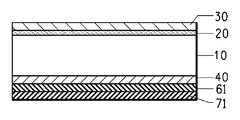
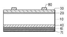
<도 1>
도 1은 종래의 공정 및 물질에 따라 반도체 디바이스를 제조하는 것을 나타낸, 측면도로 도시된 공정 흐름도.
도 1에 도시된 도면 부호는 아래에 설명되어 있다.
10: p형 규소 기판
20: n형 확산층
30: 반사 방지 코팅
40: p+ 층(후면 전계, BSF)
50: 전면 상에 형성된 은 페이스트
51: 은 전면 전극(전면 은 페이스트를 소성함으로써 얻어짐)
60: 후면 상에 형성된 알루미늄 페이스트
61: 알루미늄 후면 전극(후면 알루미늄 페이스트를 소성함으로써 얻어짐)
70: 후면 상에 형성된 은 또는 은/알루미늄 페이스트
71: 은 또는 은/알루미늄 후면 전극(후면 은 페이스트를 소성함으로써 얻어짐)
<도 2>
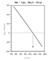
도 2는 1 대기압의 질소의 분압에서 질화규소와 다음의 금속: 니켈, 코발트, 몰리브덴, 망간 및 철 간의 반응에 대한 자유 에너지(델타 G) 대 온도의 산출 플롯.
<도 3>
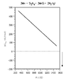
도 3은 질소의 여러 가지 분압하의 질화규소와 니켈 간의 반응에 대한 자유 에너지(델타 G) 대 온도의 산출 플롯.
<도 4>
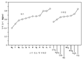
도 4는 다양한 금속 및 규화물의 n-형 규소에 대한 쇼트키 장벽 높이를 나타낸 도.
<도 5>
도 5는 본 발명에 따른, 규소 태양 전지를 제조하는 방법을 나타낸 측면도.
<도 6>
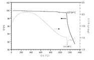
도 6은 니켈과 질화규소 분말 간 반응의 시차 열분석(DTA)과 열 중량측정 분석(TGA) 결과를 나타낸 도.
<도 7>
도 7은 니켈과 질화규소 분말에 대한 DTA/TGA 실시 후의 반응 생성물의 X-레이 분석을 나타낸 도.
<도 8>
도 8은 코발트와 질화규소 분말 간 반응의 DTA/TGA 결과를 보여주는 도.
<도 9>
도 9는 코발트와 질화규소 분말에 대한 DTA/TGA 실시 후의 반응 생성물의 X-레이 분석을 나타낸 도.
<도 10>
도 10은 70 중량% 은-30 중량% 구리-3 중량% 코발트 합금 분말과 질화규소 분말 간 반응의 DTA/TGA 결과를 보여주는 도.
<도 11>
도 11은 70 중량% 은-30 중량% 구리-3 중량% 망간 합금 분말과 질화규소 분말 간 반응의 DTA/TGA 결과를 보여주는 도.
통례에 따라, 하기에 논의된 도면의 다양한 특징부는 반드시 축척대로 도시된 것은 아니다. 도면 내의 다양한 특징부 및 요소의 치수는 본 발명의 실시 형태를 더욱 명확하게 예시하기 위하여 확대 또는 축소될 수 있다.<Figure 1>
1 is a process flow diagram depicted in a side view illustrating manufacturing a semiconductor device in accordance with conventional processes and materials.
Reference numerals shown in FIG. 1 are described below.
10: p-type silicon substrate
20: n-type diffusion layer
30: antireflective coating
40: p + layer (rear field, BSF)
50: silver paste formed on the front surface
51: silver front electrode (obtained by firing the front silver paste)
60: aluminum paste formed on the back side
61: aluminum back electrode (obtained by firing rear aluminum paste)
70: silver or silver / aluminum paste formed on the back side
71: silver or silver / aluminum back electrode (obtained by firing back silver paste)
<FIG. 2>
FIG. 2 is a plot of the free energy (delta G) versus temperature for the reaction between silicon nitride and the following metals: nickel, cobalt, molybdenum, manganese and iron at a partial pressure of nitrogen at 1 atmosphere.
3,
3 is a plot of the free energy (delta G) versus temperature for the reaction between silicon nitride and nickel under various partial pressures of nitrogen.
<Figure 4>
4 shows Schottky barrier height for n-type silicon of various metals and silicides.
<Figure 5>
5 is a side view showing a method of manufacturing a silicon solar cell according to the present invention.
6,
FIG. 6 shows differential thermal analysis (DTA) and thermal gravimetric analysis (TGA) results of a reaction between nickel and silicon nitride powder. FIG.
<Figure 7>
FIG. 7 is an X-ray analysis of the reaction product after DTA / TGA run on nickel and silicon nitride powders.
<Figure 8>
8 shows the DTA / TGA results of the reaction between cobalt and silicon nitride powder.
<Figure 9>
9 shows an X-ray analysis of the reaction product after DTA / TGA run on cobalt and silicon nitride powders.
<Figure 10>
FIG. 10 shows the DTA / TGA results of the reaction between 70 wt% silver-30 wt% copper-3 wt% cobalt alloy powder and silicon nitride powder.
<Figure 11>
FIG. 11 shows the DTA / TGA results of the reaction between 70 wt% silver-30 wt% copper-3 wt% manganese alloy powder and silicon nitride powder.
By convention, various features of the drawings discussed below are not necessarily drawn to scale. The dimensions of the various features and elements in the figures may be enlarged or reduced to more clearly illustrate embodiments of the invention.
n-형 규소에 대한 저 쇼트키 장벽 높이 전극 접점을 갖는 광기전력 디바이스가 개시되어 있다. 또한, n-형 규소에 대한 저 쇼트키 장벽 높이 전극 접점을 갖는 광기전력 디바이스를 제조하는 방법이 개시되어 있다. 개시된 광기전력 디바이스가 태양 전지이지만, 광 검출기 또는 발광 다이오드와 같은 n-형 규소에 대한 전극 접점을 갖는 다른 광기전력 디바이스일 수도 있다. 개시된 실시 형태는, n-형 규소 상의 전면 전극이 규화물을 포함하는 저 쇼트키 장벽 높이 전극 접점을 갖는 태양 전지이다.A photovoltaic device having low Schottky barrier height electrode contacts for n-type silicon is disclosed. Also disclosed is a method of manufacturing a photovoltaic device having low Schottky barrier height electrode contacts for n-type silicon. Although the disclosed photovoltaic device is a solar cell, it may be another photovoltaic device having electrode contacts to n-type silicon, such as a photo detector or light emitting diode. The disclosed embodiment is a solar cell in which the front electrode on n-type silicon has a low Schottky barrier height electrode contact comprising a silicide.
여기서 사용된 용어 "교환 금속" (M)은 질화규소와 반응하여 질화금속을 형성함이 없이 안정된 고도전성 금속과 질소 가스를 형성하는 금속 또는 금속 혼합물을 말한다. 예컨대 교환 금속은 다음 반응식에 따라 질화규소와 반응할 수 있다.The term "exchange metal" (M) as used herein refers to a metal or metal mixture that forms stable highly conductive metals and nitrogen gas without reacting with silicon nitride to form metal nitrides. For example, the exchange metal may react with silicon nitride according to the following reaction scheme.
![]()
![]()
그와 같은 금속은 니켈 (Ni), 코발트(Co), 몰리브덴(Mo), 망간(Mn), 및 철(Fe)로 이루진 그룹에서 선택된 금속 또는 그 혼합물을 포함한다. 이 금속들은 이 반응을 가능하게 하는 열역학적 특성을 갖고 있다.Such metals include metals or mixtures thereof selected from the group consisting of nickel (Ni), cobalt (Co), molybdenum (Mo), manganese (Mn), and iron (Fe). These metals have thermodynamic properties that make this reaction possible.
MSi가 바람직한 생성 규화물로서 일반적으로 나타나 있지만, 금속 함량과 반응 정도에 따라서는 다른 규화 금속도 형성될 수 있다. 그러한 규화 금속은 MxSiy로 표현될 수 있다. 여기서, M은 상기 그룹에서 선택된 금속, Si는 규소, x와 y는 금속 함량과 반응 정도에 따라서 달라질 수 있다. 조성물은 Ni3Si, Ni5Si, Ni2Si, Ni3Si2, NiSi, Co3Si, Co2Si, CoSi, Mn3Si, Mn5Si3, MnSi, Mo3Si, Mo3Si2, Fe3Si, Fe5Si3, 및 FeSi를 포함하나 이에 한정되는 것은 아니다. 조성물의 완전한 화학량론은 생기지 않을 수도 있다.Although MSi is generally shown as the preferred product silicide, other metal silicides may also be formed, depending on the metal content and the degree of reaction. Such metal silicides can be represented by M x Si y . Here, M is a metal selected from the group, Si is silicon, x and y may vary depending on the metal content and the degree of reaction. The composition is Ni 3 Si, Ni 5 Si, Ni 2 Si, Ni 3 Si 2 , NiSi, Co 3 Si, Co 2 Si, CoSi, Mn 3 Si, Mn 5 Si 3 , MnSi, Mo 3 Si, Mo 3 Si 2 , Fe 3 Si, Fe 5 Si 3 , and FeSi, but is not limited thereto. Complete stoichiometry of the composition may not occur.
여기서 사용된 용어 "비교환 금속"은 도전성 규화 금속을 생성하기 위해 질화 규소의 질소와 교환될 수 없는, 즉 질화 규소와 반응하지 않는 금속 또는 금속 혼합물을 말한다. 바람직한 비교환 금속은 용융점이 비교적 낮으므로, 교환 금속과 혼합 또는 합금되면 반응 온도가 감소하고 반응 속도가 가속될 수 있다. 공융 조성물(eutectic composition)을 사용하여 원하는 용융점을 달성하기 위해 다수의 원소를 갖는 금속 조성물이 설계될 수 있다.The term "non-exchange metal" as used herein refers to a metal or metal mixture that cannot be exchanged with the nitrogen of silicon nitride, ie, does not react with silicon nitride to produce a conductive metal silicide. Preferred non-substituted metals have a relatively low melting point, which, when mixed or alloyed with the exchange metal, can reduce the reaction temperature and accelerate the reaction rate. Metal compositions with multiple elements can be designed to achieve the desired melting point using eutectic compositions.
또한 비교환 금속은 전류 전달 특성을 향상시키기 위해 전기 저항이 비교적 작은 것이 선택된다. 비반응성 금속은 은(Ag), 구리(Cu), 주석(Sn), 비스무트(Bi), 납(Pb), 비소(As), 안티몬(Sb), 아연(Zn), 금(Au), 카드뮴(Cd), 및 베릴륨(Be)과 같은 금속의 그룹 중에서 선택될 수 있지만, 이들로 제한되지 않는다. 다른 특정의 특성을 달성하기 위해, 예를 들어, 팔라듐(Pd)과 같은 높은 용융점을 갖는 것과 같은 기타 금속이 소량 포함될 수 있다. 소량의 5 A족 원소들(인, 비소, 안티몬, 비스무트)은 도너 도펀트로서 추가적으로 작용할 수 있기 때문에 포함될 수 있다. 비교환 금속 그룹은 통상적으로 주기율표의 3족 원소(붕소(B), 알루미늄(Al), 갈륨(Ga), 인듐(In), 및 탈륨(Tl))을 포함하지 않는데, 그 이유는 이들 금속은 n-형 규소를 억셉터 도핑할 수 있고 그 표면 저항을 지나치게 크게 증가시킬 수 있기 때문이다.In addition, the non-substituted metal is selected to have a relatively low electrical resistance to improve the current transfer characteristics. Non-reactive metals are silver (Ag), copper (Cu), tin (Sn), bismuth (Bi), lead (Pb), arsenic (As), antimony (Sb), zinc (Zn), gold (Au), cadmium (Cd), and a group of metals such as beryllium (Be), but are not limited to these. In order to achieve other specific properties, small amounts of other metals may be included, such as having a high melting point such as, for example, palladium (Pd). Small amounts of Group 5 A elements (phosphorus, arsenic, antimony, bismuth) may be included because they may additionally act as donor dopants. Non-substituted metal groups typically do not contain Group 3 elements of the periodic table (boron (B), aluminum (Al), gallium (Ga), indium (In), and thallium (Tl)), because these metals This is because the n-type silicon can be acceptor-doped and its surface resistance can be excessively increased.
도 2의 산출된 플롯은 1 대기압의 질소 분압에서 질화 규소와 각종 교환 금속 간의 자유 에너지(ΔG) 대 온도를 보여준다. 금속의 질화규소와의 반응 온도의 시작은 반응 자유 에너지 델타 G가 제로인 지점에 있을 것으로 예측된다. 따라서 1 대기압에서의 유동 질소 분위기에서는 니켈만이 약 976.9℃ (1250°K)를 넘는 온도에서 질화 규소와 반응할 것으로 예측된다. 코발트, 몰리브덴, 망간, 및 철의 경우에는 반응 온도가 각각 약 1126.9℃ (1400°K), 876.9℃ (1150°K), 1376.9℃ (1650°K), 및 1326.9℃ (1600°K) 이다. 이들 온도는 통상적으로 규소 태양 전지 처리에 너무 높다. 그러나 교환 금속을 용융점이 낮은 금속과 합금하면 반응 온도를 더 낮출 수가 있다.The calculated plot of FIG. 2 shows the free energy (ΔG) versus temperature between silicon nitride and various exchange metals at a nitrogen partial pressure of 1 atmosphere. The onset of the reaction temperature of the metal with silicon nitride is expected to be at the point where the reaction free energy delta G is zero. Thus, in a flowing nitrogen atmosphere at 1 atmosphere, only nickel is expected to react with silicon nitride at temperatures above about 976.9 ° C. (1250 ° K). For cobalt, molybdenum, manganese, and iron the reaction temperatures are about 1126.9 ° C. (1400 ° K), 876.9 ° C. (1150 ° K), 1376.9 ° C. (1650 ° K), and 1326.9 ° C. (1600 ° K), respectively. These temperatures are usually too high for silicon solar cell processing. However, alloying the exchange metal with a metal with a low melting point can lower the reaction temperature.
도 3은 질소 분압을 낮추면 어떻게 니켈 반응 온도가 낮아지는 가를 보여주는 개념적인 그래프이다. 다른 금속도 비슷한 산출 그래프를 갖는다. 그러므로 반응 온도를 낮출 수 있는 방법은 질소 분압을 낮추는 것이다. 이는 예컨대 아르곤같은 불활성 기체를 이용하여 질소를 희석시킴으로써 달성될 수 있다. 일산화탄소나 수소같은 다른 기체도 희석제로 가능하다.3 is a conceptual graph showing how the nickel reaction temperature is lowered by lowering the nitrogen partial pressure. Other metals have similar output graphs. Therefore, a way to lower the reaction temperature is to lower the nitrogen partial pressure. This can be accomplished by diluting nitrogen with an inert gas such as, for example, argon. Other gases such as carbon monoxide and hydrogen can also be used as diluents.
규화니켈과 규화코발트는 n-형 규소에의 쇼트키 장벽 높이가 도 4에 도시된 바와 같이 0.6 - 0.65 eV(전자볼트) 정도이다(참조: "Barrier Heights to n-Silicon", Andrews et al., J. Vac. Sci. Tech 11, 6,972, 1974). 이는 규소 태양 전지에서 종래의 n-형 규소 접점인 은 금속(~ 0.65 eV의 ev)과 유사하다. 그러므로 규화니켈과 규화코발트는 n-형 규소에의 저 접촉 저항 접점으로는 매우 좋은 선택이다. 여기서 사용된 용어 n-형 규소에의 "저 쇼트키 장벽 높이" 접점은 접촉 저항이 0.8 eV 이하이다.Nickel silicides and cobalt silicides have Schottky barrier heights of n-type silicon on the order of 0.6-0.65 eV (electron volts) as shown in Figure 4 ("Barrier Heights to n-Silicon", Andrews et al. , J. Vac. Sci. Tech 11, 6,972, 1974). This is similar to silver metal (ev of ˜0.65 eV), which is a conventional n-type silicon contact in silicon solar cells. Nickel silicide and cobalt silicide are therefore good choices for low contact resistance contacts to n-type silicon. As used herein, the term "low Schottky barrier height" contact to n-type silicon has a contact resistance of 0.8 eV or less.
상기 금속들은 스퍼터링, 금속 증발, 화학적 기상 증착, 원자층 증착, 펄스형 레이저 증착 등을 포함하는(이에 한정되지 않음) 박막 공정에 의해 질화규소 상에 증착될 수 있다. 교환 금속과 비교환 금속은 원소 상태로 또는 독립적인 층으로서 증착되거나 동시증착되어 혼합물 또는 합금을 형성한다. 이러한 박막법에 의해 증착된 금속은 일반적으로 원하는 패턴을 정의하는 마스크 또는 포토레지스트를 통해 질화규소의 표면 상에 연속 박층으로서 증착된다.The metals may be deposited on silicon nitride by thin film processes including, but not limited to, sputtering, metal evaporation, chemical vapor deposition, atomic layer deposition, pulsed laser deposition, and the like. The exchange metal and the non-substituted metal are deposited or co-deposited in the elemental state or as independent layers to form a mixture or alloy. The metal deposited by this thin film method is generally deposited as a continuous thin layer on the surface of silicon nitride through a mask or photoresist defining a desired pattern.
금속은 또한 후막 공정에 의해서도 증착될 수 있다. 후막 공정은 스크린 프린팅, 잉크젯 프린팅 또는 포토이미징 기법을 포함하나 이에 한정되는 것은 아니다. 스크린 프린팅은 비용 효과적인 공정이라는 점에서 유리하다. 이 경우, 상기 교환 금속과 비교환 금속을 함유한 분말 형태의 페이스트는 질화규소의 표면에 스크린을 통해 프린트된다. 스크린은 원하는 패턴을 결정한다.Metals can also be deposited by thick film processes. Thick film processes include, but are not limited to, screen printing, inkjet printing or photoimaging techniques. Screen printing is advantageous in that it is a cost effective process. In this case, the paste in powder form containing the exchange metal and the non-substituted metal is printed on the surface of the silicon nitride through a screen. The screen determines the desired pattern.
교환 금속으로 제조된 스크린 프린팅 후막 페이스트에 사용하기에 적합한 분말은, 교환 금속의 자연 산화물에 의해 상기 반응이 방해받지 않도록, 가능한 한 산화물이 없어야 한다. 교환 금속은 그 산화성으로 인해 대기 중에서 실온에서 소정 두께의 산화물을 형성하므로 분말 입자의 크기가 클수록 전체 산화물 함량은 줄어든다. 따라서, 일반적으로, 산화물 레벨을 최소화하기 위해 양호한 후막 페이스트 제조 특성에 부합하는 최대 입자 크기를 갖는 분말을 사용하는 것이 바람직하다. 최적의 후막 페이스트 특성을 제공하기 위해서는 그러한 교환 금속 분말은 그 평균 직경이 0.2, 0.5, 1, 3, 5 및 10 마이크로미터 중 임의의 2가지 사이, 더 바람직하게는 0.5 내지 5 마이크로미터이어야 한다. 비교환 금속으로 제조된 적합한 분말도 가능한 한 산화물이 없어야 한다. 비교환 금속 분말은 그 평균 직경이 0.2, 0.5, 1, 3, 5 및 10 마이크로미터 중 임의의 2가지 사이, 더 바람직하게는 0.5 내지 5 마이크로미터이어야 한다.Powders suitable for use in screen printing thick film pastes made of exchange metals should be as free of oxides as possible so that the reaction is not hindered by natural oxides of the exchange metals. The exchange metal forms an oxide of a certain thickness at room temperature in the air due to its oxidizing property, so that the larger the size of the powder particles, the smaller the total oxide content. Therefore, in general, it is desirable to use a powder having a maximum particle size that meets good thick film paste manufacturing properties to minimize oxide levels. Such exchange metal powders should have an average diameter between any two of 0.2, 0.5, 1, 3, 5 and 10 micrometers, more preferably 0.5 to 5 micrometers, to provide optimum thick film paste properties. Suitable powders made of non-substituted metals should be as free of oxide as possible. The non-substituted metal powder should have an average diameter of between any two of 0.2, 0.5, 1, 3, 5 and 10 micrometers, more preferably 0.5 to 5 micrometers.
후막 증착의 경우, 상기 금속 분말은 기계적 혼합에 의해 유기 매질과 혼합되어, 프린팅에 적합한 주도(consistency) 및 리올로지를 갖는 "후막 페이스트"라고 하는 점성 조성물을 형성한다. 유기 매질은 소성 공정의 초기 단계 동안에 연소된다는 점에서 임시 재료(fugitive material)이다. 유기 물질이 완전 연소되는 온도는 후막 페이스트 조성물 중의 유기 물질의 화학적 성질과 양에 따라 다르며, 따라서 조성물은 더 낮거나 더 높은 온도에서 연소되도록 설계될 수 있다. 유기 매질은 금속 분말이 적절한 안정도로 분산가능한 것이어야 한다. 매질의 리올로지 특성은 금속 분말의 안정된 분산, 스크린 프인팅이나 기타 다른 원하는 도포 처리에 적합한 점성과 요변성(thixotropy), 기판의 적당한 페이스트 습윤성 및 양호한 건조율을 포함하는 양호한 도포성을 조성물에 부여하는 것이어야 한다. 개시된 후막 조성물에 사용되는 유기 매질은 바람직하게는 비수용성의 불활성 액체이다. 증점제, 안정제, 및/또는 다른 통상의 첨가제를 포함할 수 있거나 포함하지 않을 수 있는 임의의 다양한 유기 매질이 사용될 수 있다. 유기 매질은 전형적으로 용매(들) 중 중합체(들)의 용액이다. 더욱이, 계면활성제와 같은 소량의 첨가제가 유기 매질의 일부일 수 있다.In the case of thick film deposition, the metal powder is mixed with the organic medium by mechanical mixing to form a viscous composition called a "thick film paste" having consistency and rheology suitable for printing. The organic medium is a fugitive material in that it is burned during the initial stages of the firing process. The temperature at which the organic material is completely burned depends on the chemical nature and amount of the organic material in the thick film paste composition, and therefore the composition can be designed to burn at lower or higher temperatures. The organic medium should be one in which the metal powder is dispersible with appropriate stability. The rheological properties of the medium give the composition good coatability including viscosity and thixotropy suitable for stable dispersion of metal powders, screen printing or any other desired coating treatment, adequate paste wetting of the substrate and good drying rate. It should be. The organic medium used in the disclosed thick film compositions is preferably a water insoluble liquid. Any of a variety of organic media may be used, which may or may not include thickeners, stabilizers, and / or other conventional additives. The organic medium is typically a solution of polymer (s) in solvent (s). Moreover, small amounts of additives such as surfactants may be part of the organic medium.
유기 매질의 가장 빈번히 사용되는 중합체는 에틸 셀룰로오스이다. 유기 매질에 유용한 다른 중합체는 에틸하이드록시에틸 셀룰로오스, 나무 로진, 에틸 셀룰로오스와 페놀 수지의 혼합물, 저급 알코올의 폴리메타크릴레이트, 및 에틸렌 글리콜 모노아세테이트의 모노뷰틸 에테르를 포함한다.The most frequently used polymer of organic medium is ethyl cellulose. Other polymers useful in the organic medium include ethylhydroxyethyl cellulose, wood rosin, mixtures of ethyl cellulose and phenolic resins, polymethacrylates of lower alcohols, and monobutyl ethers of ethylene glycol monoacetate.
개시된 후막 조성물에 들어있는 가장 널리 사용되는 용매는 에스테르 알코올 및 테르펜, 예를 들어, 알파- 또는 베타-테르피네올 또는 이들과 다른 용매, 예를 들어, 등유, 다이부틸프탈레이트, 부틸 카르비톨, 부틸 카르비톨 아세테이트, 헥실렌 글리콜 및 고비점 알코올 및 알코올 에스테르의 혼합물이다. 또한, 기판 상에 도포한 후에 급속 경화를 촉진하기 위한 휘발성 액체가 비히클 내에 포함될 수 있다. 원하는 점도 및 휘발성을 얻기 위해 이들 용매 및 기타 용매의 다양한 조합이 조제된다.The most widely used solvents contained in the disclosed thick film compositions are ester alcohols and terpenes such as alpha- or beta-terpineol or other solvents such as kerosene, dibutylphthalate, butyl carbitol, butyl Carbitol acetate, hexylene glycol and mixtures of high boiling alcohols and alcohol esters. In addition, volatile liquids may be included in the vehicle to facilitate rapid curing after application onto the substrate. Various combinations of these and other solvents are formulated to achieve the desired viscosity and volatility.
유기 매질(중합체와 용매)에 존재하는 중합체는 선택된 중합체에 따라 조성물의 1 wt.% 내지 11 wt.%의 범위에 있다. 금속 조성물에 대한 후막 조성물 내의 유기 매질의 비는 페이스트를 도포하는 방법 및 사용되는 유기 매질의 종류에 따라 변할 수 있다. 일반적으로, 후막 조성물은 양호한 습윤성을 얻기 위해 70 내지 95 wt%의 금속 성분 및 5 내지 30 wt%의 유기 매질을 함유할 것이다.The polymer present in the organic medium (polymer and solvent) is in the range of 1 wt.% To 11 wt.% Of the composition, depending on the polymer selected. The ratio of the organic medium in the thick film composition to the metal composition may vary depending on the method of applying the paste and the type of organic medium used. In general, the thick film composition will contain 70 to 95 wt% of the metal component and 5 to 30 wt% of the organic medium to obtain good wettability.
저 쇼트키 장벽 높이 접점(규화금속을 형성하기 위해 교환 금속을 질화규소 중의 질소와 교환함으로써 얻음)은 그 두께가 질화규소층의 두께(70 내지 100 나노미터)와 거의 같을 수 있으며, 또는 소성 공정, 교환 금속 증착량 및 하부의 n-형 규소와의 반응 여부에 따라서 수 마이크로미터 정도가 될 수 있다. 그렇지만, 전류를 외부 회로에 전달하기 위해 저저항 전류 캐리어(current carrier)를 형성하는 것도 유익하다. 즉, 저항이 작은 전극 또는 부가 금속층이 바람직하다. 이는 소성 공정 전에 교환 금속층 위에 비교환 금속층 증착함으로써 달성될 수 있다. 다른 방법은 교환 금속을 비교환 금속과 동시에 적절한 양으로 증착하는 것이다. 이 동시-증착법은 금속의 혼합물 또는 교환 금속과 비교환 금속의 합금을 포함할 수 있다. 혼합물 또는 합금 조성물 내의 교환 금속의 양은 질화규소의 두께, 교환 금속 및 증착의 두께에 맞게 정해진다. 통상적으로 교환 금속은 조성물 중의 금속의 약 1-40 wt%를 포함할 것이며, 비교환 금속은 조성물 중의 금속의 약 99-60 wt%를 포함할 것이다.Low Schottky barrier height contacts (obtained by exchanging exchange metals with nitrogen in silicon nitride to form metal silicides) may be about the same thickness as the silicon nitride layer (70-100 nanometers), or firing process, exchange It may be several micrometers depending on the amount of metal deposition and the reaction with the n-type silicon at the bottom. However, it is also beneficial to form a low resistance current carrier to transfer current to an external circuit. That is, the electrode or the additional metal layer with low resistance is preferable. This can be accomplished by depositing a non-substituted metal layer on the exchange metal layer prior to the firing process. Another method is to deposit the exchange metal in an appropriate amount simultaneously with the non-substituted metal. This co-deposition method may include a mixture of metals or an alloy of exchange metals and non-substituted metals. The amount of exchange metal in the mixture or alloy composition is adapted to the thickness of the silicon nitride, the exchange metal and the thickness of the deposition. Typically the exchange metal will comprise about 1-40 wt% of the metal in the composition and the non-substituted metal will comprise about 99-60 wt% of the metal in the composition.
본 명세서에 기술된 저 쇼트키 장벽 높이 전극 접점을 갖는 태양 전지는 다음과 같은 방법에 의해 제조될 수 있다.Solar cells having low Schottky barrier height electrode contacts described herein can be manufactured by the following method.
도 5를 참조하면, 도 5A에 도시된 물품이 제공된다. 이 물품은 단결정 규소 또는 다결정 규소를 함유할 수 있고, p-형 규소 기판(10), n-형 확산층(20), 및 반사 방지 코팅(30)을 포함한다. 도 5A에 도시된 물품은 도 1D에 도시된 물품과 관련하여 상기한 바와 같이 제작될 수 있다.Referring to FIG. 5, an article shown in FIG. 5A is provided. The article may contain monocrystalline silicon or polycrystalline silicon and includes a p-
도 5를 참조하면, 도 1D의 물품이 제공되고 도 5A로서 도시되어 있다. 도 5B를 참조하면, 알루미늄 페이스트(60) 및 후면 은 또는 은/알루미늄 페이스트(70)가 기판의 후면에 연속하여 스크린 프린팅되고 건조된다. 이어서, 후면 페이스트의 소성이 적외선 노에서 대략 700℃ 내지 975℃의 온도 범위에서 몇 분 내지 몇십 분의 기간 동안 공기 중에서 실시된다. 이 소성에 따라 도 5C의 물품이 생성된다.Referring to FIG. 5, the article of FIG. 1D is provided and shown as FIG. 5A. 5B,
도 5C를 참조하면, 종래의 공정에서와 같이, 소성 동안에 알루미늄이 알루미늄 페이스트로부터 규소 기판(10) 내로 도펀트로서 확산되어, 고농도의 알루미늄 도펀트를 함유하는 p+ 층(40)을 형성한다.Referring to FIG. 5C, as in the conventional process, aluminum is diffused as a dopant from the aluminum paste into the
소성은 알루미늄 페이스트(60)를 알루미늄 후면 전극(61)으로 변환시킨다. 후면 은 또는 은/알루미늄 페이스트(70)가 동시에 소성되어, 은 또는 은/알루미늄 후면 전극(71)으로 된다. 소성 동안에, 후면 알루미늄과 후면 은 또는 은/알루미늄 사이의 경계가 합금 상태를 띠고, 그로써 전기적 접속을 달성한다. 알루미늄 전극이, 부분적으로는 p+ 층(40)을 형성할 필요성으로 인해, 후면 전극의 대부분의 영역을 차지한다. 알루미늄 전극에 솔더링하는 것이 불가능하기 때문에, 은 후면 탭 전극(silver back tab electrode)이 구리 리본 등에 의해 태양 전지들을 상호접속시키는 전극으로서 후면의 일부분 상에 형성된다.Firing converts the
본 명세서에 기술된 새로운 교환 금속 조성물(들)이 이제 후막 또는 박막 증착 공정에 의해 질화규소 절연막(30) 상에 도 5D에서 80으로 도시된 전면 전극의 핑거(finger) 및/또는 부스바(bussbar)에 대응하는 패턴으로 도포된다. 이 증착은 동일 패턴 상에의 교환 금속과 비교환 금속의 순차적 증착(도 5D에서 단일층(80)으로서 도시된 양 층) 또는 교환 금속과 비교환 금속의 혼합물 또는 교환 금속/비교환 금속 합금의 1회 증착에 의해 달성될 수 있다.The new exchange metal composition (s) described herein are now finger and / or busbar of the front electrode shown at 80 in FIG. 5D on silicon
증착된 금속 조성물(들)이 이제 소성된다. 소성은 통상적으로 노에서 400℃ 내지 950℃ 범위 내의 온도에서 행해지며, 실제의 온도는 금속 조성물에 따라 다르다. 이 범위의 하단의 온도에서의 소성이 바람직할 수 있는데, 그 이유는 금속 산화가 크게 줄어들 것이기 때문이다. 소성은 진공, 순수 질소 기체, 수소와 질소의 혼합물 또는 아르곤, 일산화탄소 및/또는 수증기와 같은 기타 기체들의 혼합물을 포함할 수 있는 보호성 분위기에서 행해진다.. 그와 같은 기체 혼합물은 교환 금속과 비교환 금속의 산화를 막기 위해 소성 공정 중에 산소와 질소의 분압을 조절하는데 이용될 수 있다. 산화를 방지하는 데 필요한 정확한 산소 분압(PO2)은 금속 조성물에 따라 다르다. 금속을 산화로부터 완전히 보호하는 분위기는, "F. D. Richardson and J.H. E Jeffes, J. Iron Steel Inst., 160, 261 (1948)에 개시된 바와 같이, 온도 계산 또는 다이어그램의 함수로서 산화물의 표준 생성 자유 에너지로부터 열역학적으로 도출될 수 있다. 그러나, 일반적으로는 산소 분압(PO2)이 대략 10-6 내지 10-14 대기압 정도인 것이 적당하다. 이것은 일반적으로 순수 질소, 일산화탄소/이산화탄소 혼합물, 아르곤, 형성 가스(질소 중의 1-4% 수소), 수소와 아르곤의 혼합물, 또는 진공의 사용에 의해 달성될 수 있다. 아르곤과 같은 중성 기체는 질소를 희석시키고 반응 온도를 낮추기 때문에 유리할 수 있다. 이산화탄소와 일산화탄소도 질소를 희석시키는데 이용될 수 있다. 추가적인 보호를 위해서는 일산화탄소와 수소를 포함하는 현장(in-situ) 환원성 분위기가 유기 매질의 열분해 중에 의도적으로 형성될 수 있다. 더 높은 온도가 될 때까지 연소되지 않는 매질이 이를 달성할 수 있다. 그 외에도, 분해 중에 일산화탄소와 수소를 생성하도록 특별히 고안된 유기 물질이 페이스트에 첨가될 수도 있다. 그와 같은 첨가제로는 포름산염, 아세테이트 등이 있다. 유기물의 열분해로부터의 현장 환원성 환경은, 어떤 상황에서는 보호성 분위기를 이용하지 않더라도 공기 중 소성이 달성될 수 있도록, 유기 매질의 화학적 성질과 함량에 의해 조절될 수 있다. 티타늄 플레이트나 세터와 같은 산소 겟터도 기체로부터 산소를 배기하는데 이용될 수 있으며, 또는 보호 용제가 이용된다.The deposited metal composition (s) are now fired. Firing is usually carried out in a furnace at temperatures in the range of 400 ° C. to 950 ° C., and the actual temperature depends on the metal composition. Firing at temperatures below this range may be desirable because metal oxidation will be greatly reduced. Firing is carried out in a protective atmosphere, which may include vacuum, pure nitrogen gas, a mixture of hydrogen and nitrogen, or a mixture of other gases such as argon, carbon monoxide and / or water vapor. Such gas mixtures are not compatible with exchange metals. It can be used to control the partial pressures of oxygen and nitrogen during the firing process to prevent oxidation of the exchange metal. The exact oxygen partial pressure (PO 2) needed to prevent oxidation depends on the metal composition. The atmosphere that completely protects the metal from oxidation is described by the standard production free energy of the oxide as a function of temperature calculation or diagram, as disclosed in "FD Richardson and JH E Jeffes, J. Iron Steel Inst., 160, 261 (1948). Thermodynamically, but generally it is appropriate that the oxygen partial pressure (PO2) is approximately 10 −6 to 10 −14 atmospheric pressure, which is generally pure nitrogen, carbon monoxide / carbon dioxide mixtures, argon, forming gases (nitrogen). 1-4% hydrogen), a mixture of hydrogen and argon, or a vacuum.Neutral gases such as argon may be advantageous because they dilute nitrogen and lower the reaction temperature. For additional protection, an in-situ reducing atmosphere containing carbon monoxide and hydrogen may be used to It can be intentionally formed during decomposition, a medium which does not combust until a higher temperature can be achieved, in addition, organic materials specially designed to produce carbon monoxide and hydrogen during decomposition may be added to the paste. Such additives include formate, acetate, etc. The in situ reducible environment from thermal decomposition of organics is such that in some situations the chemical properties and content of the organic medium are such that firing in the air can be achieved without using a protective atmosphere. Oxygen getters such as titanium plates or setters can also be used to evacuate oxygen from the gas, or protective solvents can be used.
적당한 용제에 의한 보호가 이용되는 경우에는 공기 중 소성이 실행가능하다.Firing in air is feasible when protection with a suitable solvent is used.
용제는 금속의 납땜, 경납땜 및 용접 분야에 잘 알려져 있으며, 용융 금속이 산화되는 것을 방지하는데 이용된다. 교환 금속을 위한 용제는 예컨대 나트륨, 리튬, 칼륨 및 세슘과 같은 주기율표의 1족 금속의 불화물과 염화물의 혼합물일 수 있다. 예컨대 염화 암모늄, 인산수소 암모늄, 붕산, 붕소, 붕사 및 유기 할로겐화물같은 다른 화합물도 포함될 수 있다. 용제가 페이스트로서 도포되어 교환 금속층(도면에는 미도시)의 표면 위에 어떤 층을 형성할 수 있고, 또는 후막 증착 공정이 이용되는 경우에는 후막 금속 페이스트에 용제 분말이 첨가될 수 있다. 용제는 분말 상의 코팅으로 이용될 수도 있다. 용제는 비교적 낮은 온도에서 녹을 수 있도록 조제되며 금속 산화물을 용해시켜 금속이 산화물이 없는 깨끗한 표면을 유지할 수 있도록 해주며, 용제는 소성 공정 후에 씻겨 없어지도록 수용성으로 될 수 있다.Solvents are well known in the field of soldering, brazing and welding metals and are used to prevent the molten metal from oxidizing. Solvents for exchange metals may be mixtures of fluorides and chlorides of Group 1 metals of the periodic table, such as sodium, lithium, potassium and cesium. Other compounds such as, for example, ammonium chloride, ammonium hydrogen phosphate, boric acid, boron, borax and organic halides may also be included. The solvent may be applied as a paste to form a layer on the surface of the exchange metal layer (not shown in the figure), or solvent powder may be added to the thick film metal paste when a thick film deposition process is used. The solvent may be used as a coating on the powder. Solvents are formulated to melt at relatively low temperatures, dissolve the metal oxides to keep the metals clean and free of oxides, and the solvents can be water soluble to be washed away after the firing process.
이상적으로는, 후막 공정에서 후막 페이스트에 용제가 포함된다면 이 용제는 유기 매질이 열분해되기 전에 소정 온도에서 약간 녹을 수 있도록 조제된다. 유기 매질의 열분해가 종료할 때까지 그 동안에 증착물의 유기 함량때문에 보호성 환경이 계속 유지될 것이다. 열분해가 종료되고 나면 무기 용제가 보호막 역할을 하게 된다.Ideally, if the thick film paste contains a solvent in the thick film process, the solvent is formulated to be slightly soluble at a predetermined temperature before the organic medium is pyrolyzed. The protective environment will continue to be maintained because of the organic content of the deposit during the thermal decomposition of the organic medium. After pyrolysis, the inorganic solvent acts as a protective film.
소성 공정 중에 용융 교환 금속 합금을 형성하는 것이우선적일 수 있다. 용융 금속은 액상(liquid phase)의 지원을 통한 변환 속도(transformation kinetics)의 가속화로 인해 변환 반응 온도의 저하를 가능하게 해준다. 교환 금속이 먼저 증착되고 이어서 비교환 금속이 증착되는 경우, 또는 양 금속이 혼합물로서 증착되는 경우에는 비교환 금속이 녹아서 교환 금속을 빠르게 용해시켜 용융 금속을 형성한다. 증착된 합금의 경우에는 금속이 녹아 용융 합금을 형성한다. 금속이 용융되는 동안, 교환 금속이 우선적으로 용융 금속으로부터 질화규소 계면으로 이동하여 질화규소와 반응하여 교환 금속 규화물을 형성한다. 이 계면에서 교환 금속이 고갈됨에 따라, 더 많은 교환 금속이 반응하기 위해 계면으로 이동한다. 이것은 용융 합금 내의 교환 금속이 금속 규화물을 형성하는 데 소비될 때까지 또는 소성 공정의 중단에 의해 반응이 종료될 때까지 계속된다. 이 공정에서 용융 금속을 포함시키면 질화규소를 교환 금속 규화물로 변환시키는 속도(kinetics)를 가속시키며 그에 따라 소성이 400℃ 내지 950℃와 같은 비교적 낮은 온도에서 달성될 수 있다.It may be a priority to form the melt exchange metal alloy during the firing process. Molten metals enable lowering of the conversion reaction temperature due to the acceleration of the transformation kinetics through the support of the liquid phase. When the exchange metal is deposited first and then the non-substituted metal is deposited, or when both metals are deposited as a mixture, the non-substituted metal melts to quickly dissolve the exchange metal to form a molten metal. In the case of the deposited alloy, the metal melts to form a molten alloy. While the metal is molten, the exchange metal preferentially migrates from the molten metal to the silicon nitride interface and reacts with the silicon nitride to form an exchange metal silicide. As the exchange metal is depleted at this interface, more exchange metal moves to the interface for reaction. This continues until the exchange metal in the molten alloy is consumed to form metal silicides or until the reaction is terminated by stopping the firing process. Inclusion of molten metal in this process accelerates the kinetics of converting silicon nitride to exchange metal silicides and thus firing can be achieved at relatively low temperatures, such as 400 ° C to 950 ° C.
도 5E를 참조하면, 소성은 다음과 같은 요소를 포함하는 전극을 형성한다: a) 반사 방지 코팅(30)의 변환으로부터 형성되고 아래의 n-형 규소(20)에 반응 결합되는 제1 규화물 층(90), b) 용융 금속으로부터 형성되는 제2 금속층(92). 이 공정에서 용제가 사용되면 이 용제는 소성 후에도 전극 표면에 남게 될 것이지만 소성 후에 씻겨 없어질 수 있다.Referring to FIG. 5E, the firing forms an electrode comprising the following elements: a) a first silicide layer formed from the transformation of the
소성 공정 중에 용융 교환 금속 합금을 형성하는 것이 우선적일 수 있지만, 소성이 비교환 금속을 용융시키지 않고 변환 공정이 용융없이 고체 상태에서 일어나는 것도 전적으로 실행가능하다. 마지막으로, 또한 본 명세서에 기술된 새로운 조성물(들)이 후면 페이스트와 동시 소성될 수 있도록 본 명세서에 기술된 공정 단계가 수정될 수 있는 것도 가능하다.Although forming the molten exchange metal alloy during the firing process may be preferred, it is also entirely feasible that firing does not melt the non-ring metal and the conversion process occurs in the solid state without melting. Finally, it is also possible that the process steps described herein can be modified so that the new composition (s) described herein can be co-fired with the backside paste.
실시예Example
실시예 1Example 1
1:1 체적비의 1 마이크로미터 직경 니켈 분말과 질화규소 결정 분말 혼합물을 모르타르와 막자(pestle)를 이용하여 제작하였다. 이 혼합물을 질소 분위기 하에서 약 1300℃까지 가열하여 DTA/TGA(simultaneous differential thermal analysis/thermal gravimetric analysis)를 실시하였다. 이러한 혼합물은 DTA/TGA 실시 중에 알루미늄 도가니에 담겼다. 질소 유속은 100mL/min이었다. 가열속도는 10℃/min이였다. 도 6은 DTA/TGA 실시 결과를 보여준다. TGA에 의해 알 수 있는 것과 같이, 약 1225℃에서 반응이 시작되었고, 이에 따라 질화규소로부터의 질소 배출을 의미하는 약 10% 정도의 중량 손실이 발생하였다. 같은 온도에서 DTA 실시 시에 흡열이 관찰되었는데, 이는 용융을 의미한다. 니켈은 1453℃에서 녹기때문에, 이 같은 용융 흡열은 니켈과 규소의 합금화가 발생하였다는 것을 의미한다. 니켈-규소 상도(phase diagram)(참조: "Constitution of Binary Alloys", Max Hansen, Second Edition, McGraw Hill, 1958)로부터 알 수 있듯이, 니켈과 합금화된 10 wt% 규소는 용융점을 약 1200℃로 낮춘다. 도 7은 TGA/DTA 실시 후의 그 혼합물의 X-레이 회절을 보여준다. 이는 규화니켈 함량이 높은 것을 보여주며, 이것은 용융 흡열이 규화니켈 형성에 기인한 것임을 확인시켜 준다. 반응하지 않은 니켈과 반응하지 않은 질화규소의 잔량도 존재하였다.A 1 micron diameter nickel powder and silicon nitride crystal powder mixture in a 1: 1 volume ratio was prepared using mortar and pestle. The mixture was heated to about 1300 ° C. under a nitrogen atmosphere to conduct simultaneous differential thermal analysis / thermal gravimetric analysis (DTA / TGA). This mixture was placed in an aluminum crucible during the DTA / TGA run. Nitrogen flow rate was 100 mL / min. The heating rate was 10 ° C./min. 6 shows the results of DTA / TGA implementation. As can be seen by the TGA, the reaction started at about 1225 ° C., resulting in a weight loss of about 10%, meaning nitrogen emissions from silicon nitride. At the same temperature, an endotherm was observed during the DTA run, which means melting. Since nickel melts at 1453 ° C., this melting endotherm means that nickel and silicon alloyed. As can be seen from the nickel-silicon phase diagram ("Constitution of Binary Alloys", Max Hansen, Second Edition, McGraw Hill, 1958), 10 wt% silicon alloyed with nickel lowers the melting point to about 1200 ° C. . 7 shows the X-ray diffraction of the mixture after TGA / DTA run. This shows that the nickel silicide content is high, which confirms that the melting endotherm is due to the nickel silicide formation. There was also a balance of unreacted nickel and unreacted silicon nitride.
실시예 2Example 2
1:1 체적비의 1 마이크로미터 직경 코발트 분말과 질화규소 결정 분말 혼합물을 모르타르와 막자를 이용하여 제작하였다. 이 혼합물을 질소 분위기 하에서 약 1300℃까지 가열하여 동시적인 DTA/TGA를 실시하였다. 이러한 혼합물은 DTA/TGA 실시 중에 알루미늄 도가니에 담겼다. 질소 유속은 100mL/min이었다. 가열속도는 10℃/min이었다. 도 8은 DTA/TGA 실시 결과를 보여준다. TGA에 의해 알 수 있는 것과 같이, 약 1137℃에서 반응이 시작되었고, 이에 따라 질화규소로부터의 질소 배출을 의미하는 약 9% 정도의 중량 손실이 발생하였다. 유사한 온도에서 DTA 실시 시에 흡열이 관찰되었는데, 이는 용융을 의미한다. 코발트는 1495℃에서 녹기때문에, 이 같은 용융 흡열은 코발트와 규소의 합금화가 발생하였다는 것을 의미한다. 코발트-규소 상도(참조: "Constitution of Binary Alloys", Max Hansen, Second Edition, McGraw Hill, 1958)로부터 알 수 있듯이, 코발트와 합금화된 약 12 wt% 규소는 용융점을 약 1200℃로 낮춘다. 도 9는 TGA/DTA 실시 후의 그 혼합물의 X-레이 회절을 보여준다. 이는 규화니켈 함량이 높은 것을 보여준다. TGA는 1141℃에서 용융이 일어났음을 보여주고 상도는 규화코발트의 최저 용융 온도가 약 1200℃임을 나타내지만, 그 차이는 그 용융이 규화코발트의 용용이었고 용융점은 아마도 질소때문에 약간 감소하였다고 생각할 수 있을 정도로 충분히 작다. 반응하지 않은 코발트도 존재하였다. 질화규소는 검출되지 않았다.A 1 micron diameter cobalt powder and silicon nitride crystal powder mixture in a 1: 1 volume ratio were prepared using mortar and pestle. This mixture was heated to about 1300 ° C. under a nitrogen atmosphere to effect simultaneous DTA / TGA. This mixture was placed in an aluminum crucible during the DTA / TGA run. Nitrogen flow rate was 100 mL / min. The heating rate was 10 ° C./min. 8 shows the results of the DTA / TGA implementation. As can be seen by the TGA, the reaction started at about 1137 ° C., resulting in a weight loss of about 9%, meaning nitrogen emissions from silicon nitride. An endotherm was observed upon running DTA at similar temperatures, which means melting. Since cobalt melts at 1495 ° C., this melting endotherm means that cobalt and silicon alloyed. As can be seen from the cobalt-silicon phase ("Constitution of Binary Alloys", Max Hansen, Second Edition, McGraw Hill, 1958), about 12 wt% silicon alloyed with cobalt lowers the melting point to about 1200 ° C. 9 shows the X-ray diffraction of the mixture after TGA / DTA run. This shows that the nickel silicide content is high. TGA shows that melting took place at 1141 ° C and the top coat indicates that the lowest melting temperature of cobalt silicide is about 1200 ° C, but the difference is that the melting was a melt of cobalt silicide and the melting point was probably slightly reduced due to nitrogen. Small enough to be Unreacted cobalt was also present. Silicon nitride was not detected.
실시예 3Example 3
70 wt.% 은 - 27 wt.% 구리- 3 wt.% 망간 합금 분말이 질화규소 분말과 1:1 체적비로 모르타르와 막자를 이용하여 혼합되었다. 이 혼합물을 질소 분위기 하에서 약 1300℃까지 가열하여 동시적인 DTA/TGA를 실시하였다. 이러한 혼합물은 DTA/TGA 실시 중에 알루미늄 도가니에 담겼다. 질소 유속은 100mL/min이었다. 가열속도는 10℃/min이었다. 도 10은 DTA/TGA 실시 결과를 보여준다. TGA에 의해 알 수 있는 것과 같이, 약 737℃에서 반응이 시작되었고, 이에 따라 질화규소로부터의 질소 배출을 의미하는 3%보다 약간 적은 정도의 중량 손실이 발생하였다. 약 780℃에서 DTA 실시 시에 약간의 발열과 약간의 흡열이 관찰되었는데, 이는 발열점에서 반응이 일어났고 흡열점에서 용융이 일어났음을 의미한다. 추가로, 약 810℃에서 흡열이 관찰된다. 은-구리 비율은 779℃의 용융점을 가지는 합금을 생성하고, 망간이 이러한 용융점을 다소 높이기 때문에, 810℃에서의 흡열은 합금의 용융이 발생했다는 것을 암시한다.70 wt.% Silver-27 wt.% Copper-3 wt.% Manganese alloy powder was mixed with silicon nitride powder using mortar and pestle in a 1: 1 volume ratio. This mixture was heated to about 1300 ° C. under a nitrogen atmosphere to effect simultaneous DTA / TGA. This mixture was placed in an aluminum crucible during the DTA / TGA run. Nitrogen flow rate was 100 mL / min. The heating rate was 10 ° C./min. 10 shows the results of DTA / TGA implementation. As can be seen by the TGA, the reaction started at about 737 ° C., resulting in a weight loss of slightly less than 3%, meaning nitrogen emissions from silicon nitride. A slight exotherm and a slight endotherm was observed upon DTA at about 780 ° C., indicating a reaction at the exothermic point and melting at the endothermic point. In addition, endotherms are observed at about 810 ° C. Since the silver-copper ratio produced an alloy with a melting point of 779 ° C. and manganese somewhat increased this melting point, the endotherm at 810 ° C. suggests that melting of the alloy occurred.
실시예 4Example 4
70 wt.% 은 - 27 wt.% 구리- 3 wt.% 코발트 합금 분말이 질화규소 분말과 1:1 체적비로 모르타르와 막자를 이용하여 혼합되었다. 이 혼합물을 질소 분위기 하에서 약 1300℃까지 가열하여 동시적인 DTA/TGA를 실시하였다. 이러한 혼합물은 DTA/TGA 실시 중에 알루미늄 도가니에 담겼다. 질소 유속은 100mL/min이었다. 가열속도는 10℃/min이었다. 도 11은 DTA/TGA 실시 결과를 보여준다. TGA에 의해 알 수 있는 것과 같이, 약 737℃에서 반응이 시작되었고, 이에 따라 질화규소로부터의 질소 배출을 의미하는 3%보다 약간 적은 정도의 중량 손실이 발생하였다. DTA 실시 시에 유사한 온도에서 발열이 있었고 이보다 높은 온도인 약 885℃에서는 흡열이 관찰되었는데, 이는 이 합금이 용융되었음을 암시한다.70 wt.% Silver-27 wt.% Copper-3 wt.% Cobalt alloy powder was mixed with silicon nitride powder using mortar and pestle in a 1: 1 volume ratio. This mixture was heated to about 1300 ° C. under a nitrogen atmosphere to effect simultaneous DTA / TGA. This mixture was placed in an aluminum crucible during the DTA / TGA run. Nitrogen flow rate was 100 mL / min. The heating rate was 10 ° C./min. 11 shows the results of DTA / TGA implementation. As can be seen by the TGA, the reaction started at about 737 ° C., resulting in a weight loss of slightly less than 3%, meaning nitrogen emissions from silicon nitride. There was an exotherm at a similar temperature during the DTA run and an endotherm was observed at a higher temperature, about 885 ° C., suggesting that the alloy was molten.
실시예 1과 2는 질화규소가 코발트 및 니켈 분말과 반응하여 질소가 배출된 규화물을 형성할 수 있음을 보여준다. 질소 분위기에서 반응하면, 니켈에 대해서는 약 1225℃에서 코발트에 대해서는 1137℃에서 반응이 개시된다. 이 온도들은 도 3의 열역학적 계산이 제시하는 온도와는 약간 다르다. 이 차이는 형성된 규화물 전부가 화학량론적 1:1 금속 규화물인 것이 아니고 따라서 형성 자유 에너지가 예측된 것과 약간 다를 수 있다는 사실에 기인할 수 있다.Examples 1 and 2 show that silicon nitride can react with cobalt and nickel powders to form nitrogen released silicides. When reacting in a nitrogen atmosphere, the reaction is initiated at about 1225 ° C for nickel and 1137 ° C for cobalt. These temperatures are slightly different from those suggested by the thermodynamic calculations of FIG. 3. This difference may be due to the fact that not all of the formed silicides are stoichiometric 1: 1 metal silicides and therefore the formation free energy may be slightly different than expected.
실시예 3과 4는 질화규소 분말을 니켈 또는 코발트보다 용융점이 상당히 낮은 합금 분말과 반응시킨 것이었다 70 wt% 은 대 27 wt% 구리의 비율은 은과 구리의 공융 조성물(eutectic composition)을 나타낸다. 그 용융점은 779℃이다. 망간은 1245℃에서 용융하고 이에 따라 구리 은 공융 조성물에 3 wt%의 망간을 첨가하는 것은 용융점을 800℃를 조금 초과하는 온도로 높인다. 코발트는 1495℃에서 용융하고 이에 따라 구리 은 공융 조성물에 3 wt%의 코발트를 첨가하는 것은 용융점을 약 880℃로 높인다. 이는 DTA 실시시 증명된다. 코발트 또는 망간의 양은 규소 태양전지 전방 표면 금속화에 사용될 때 저 용융점 합금에 필요한 근사량이 되게 설계되었다. TGA 실시에서 보듯이, 양 합금에 대해서 약 737℃에서 반응이 시작되는데, 그 결과, 3% 보다 약간 적은 중량 손실이 생긴다. 반응하는 분말을 X-레이 분석해보았지만 농도가 낮아서 감도가 충분치 못해 규화물을 보여주지는 못했다. 명확히는 증명되지는 않았지만, 중량 손실의 가장 큰 원인은 질소 배출이며, 이는 소량의 교환 금속을 함유한 용융점이 비교적 낮은 합금이 적당한 온도에서 질화규소와 반응하여 전류 캐리어로서 기능할 수 있는 주 비교환 금속층과 함께 저 쇼트키 장벽 높이 금속 규화물층을 형성할 것임을 보여준다.Examples 3 and 4 reacted silicon nitride powders with alloy powders with significantly lower melting points than nickel or cobalt. The ratio of 70 wt% silver to 27 wt% copper represents an eutectic composition of silver and copper. Its melting point is 779 ° C. Manganese melts at 1245 ° C. and therefore adding 3 wt% of manganese to the copper silver eutectic composition raises the melting point to a temperature slightly above 800 ° C. Cobalt melts at 1495 ° C., thus adding 3 wt% of cobalt to the copper silver eutectic composition raises the melting point to about 880 ° C. This is demonstrated in the implementation of the DTA. The amount of cobalt or manganese is designed to be an approximation required for low melting point alloys when used for silicon solar cell front surface metallization. As seen in the TGA implementation, the reaction starts at about 737 ° C. for both alloys, resulting in slightly less than 3% weight loss. X-ray analysis of the reacted powders showed low concentrations, but not enough sensitivity to show silicides. Although not clearly demonstrated, the largest source of weight loss is nitrogen emissions, which is a major non-substituted metal layer in which a relatively low melting point alloy containing a small amount of exchange metal can function as a current carrier by reacting with silicon nitride at a suitable temperature. And a low Schottky barrier height metal silicide layer.
Claims (20)
p-형 규소 베이스와 n-형 규소층을 구비한 규소 기판을 제공하는 단계;
상기 규소 기판의 상기 n-형 규소층에 질화규소층을 형성하는 단계;
교환 금속을 상기 질화규소층과 접촉하게 배치하는 단계;
비교환 금속을 상기 교환 금속에 접촉하게 배치하는 단계;
상기 n-형 규소층에의 금속 질화물 접점과 상기 금속 질화물 접점과 접촉하는 도전성 금속 전극을 형성하기 위하여 상기 규소 기판, 질화규소층, 교환 금속 및 비교환 금속을 소성하는 단계를 포함하는 광기전력 디바이스 제조 방법.A method of manufacturing a photovoltaic device,
providing a silicon substrate having a p-type silicon base and an n-type silicon layer;
Forming a silicon nitride layer on the n-type silicon layer of the silicon substrate;
Disposing an exchange metal in contact with the silicon nitride layer;
Disposing a non-substituted metal in contact with the exchange metal;
Fabricating the silicon substrate, silicon nitride layer, exchange metal and non-substituted metal to form a metal nitride contact to the n-type silicon layer and a conductive metal electrode in contact with the metal nitride contact. Way.
p-형 규소 베이스와 n-형 규소층을 구비한 규소 기판을 제공하는 단계;
상기 규소 기판의 상기 n-형 규소층에 질화규소 반사 방지층을 형성하는 단계;
교환 금속을 상기 질화규소 반사 방지층과 접촉하게 배치하는 단계;
비교환 금속을 상기 교환 금속에 접촉하게 배치하는 단계;
상기 n-형 규소층에의 금속 질화물 접점과 상기 금속 질화물 접점과 접촉하는 도전성 금속 전극을 형성하기 위하여 상기 규소 기판, 질화규소층, 교환 금속 및 비교환 금속을 소성하는 단계를 포함하는 규소 태양 전지 제조 방법.In the method of manufacturing a silicon solar cell,
providing a silicon substrate having a p-type silicon base and an n-type silicon layer;
Forming a silicon nitride anti-reflection layer on the n-type silicon layer of the silicon substrate;
Disposing an exchange metal in contact with the silicon nitride antireflective layer;
Disposing a non-substituted metal in contact with the exchange metal;
Firing the silicon substrate, the silicon nitride layer, the exchange metal, and the non-substituted metal to form a metal nitride contact to the n-type silicon layer and a conductive metal electrode in contact with the metal nitride contact. Way.
상기 비교환 금속은 은, 구리, 주석, 비스무트, 납, 안티몬, 비소, 아연, 금, 카드뮴 및 베릴륨으로 이루어진 그룹에서 선택된 하나 이상의 금속인 규소 태양 전지 제조 방법.The method of claim 13, wherein the exchange metal is at least one metal selected from the group consisting of nickel, cobalt, iron, manganese and molybdenum,
And the non-substituted metal is at least one metal selected from the group consisting of silver, copper, tin, bismuth, lead, antimony, arsenic, zinc, gold, cadmium, and beryllium.
니켈, 코발트, 철, 망간, 몰리브덴 및 그 조합으로 이루어진 그룹에서 선택된 하나 이상의 교환 금속; 및
은, 구리, 주석, 비스무트, 납, 안티몬, 비소, 아연, 금, 카드뮴, 베릴륨 및 그 조합 중에서 선택된 하나 이상의 비교환 금속을 포함하고,
상기 교환 금속과 비교환 금속은 유기 매질 중에 있고, 및
상기 교환 금속과 비교환 금속은 그 평균 직경이 0.2 내지 10 마이크로미터 범위인 입자 형태로 된 후막 조성물.In a thick film composition for forming an electrical contact on a silicon nitride antireflection layer of a photovoltaic cell,
At least one exchange metal selected from the group consisting of nickel, cobalt, iron, manganese, molybdenum and combinations thereof; And
At least one non-substituted metal selected from silver, copper, tin, bismuth, lead, antimony, arsenic, zinc, gold, cadmium, beryllium, and combinations thereof,
The exchange metal and the non-substituted metal are in an organic medium, and
The exchange metal and the non-substituted metal thick film composition in the form of particles having an average diameter of 0.2 to 10 micrometers range.
상기 n-형 규소층 상에 배치되어 고착되고, 니켈, 코발트, 철, 망간, 몰리브덴 및 그 조합으로 이루어진 그룹에서 선택된 금속의 규화물로 구성되고, 그 접촉 저항이 0.8eV 이하인 상기 n-형 규소층에의 저 쇼트키 장벽 높이 접점을 제공하는 접점; 및
상기 금속 규화물 접점 상에 고착 배치되고, 은, 구리, 주석, 비스무트, 납, 안티몬, 비소, 아연, 게르마늄, 금, 카드뮴, 베릴륨 및 그 조합으로 이루어진 그룹 중에서 선택된 도전성 금속으로 구성된 도전성 금속 전극을 포함하는 광기전력 디바이스.
a substrate comprising an n-type silicon layer;
The n-type silicon layer disposed on and fixed to the n-type silicon layer and composed of a silicide of a metal selected from the group consisting of nickel, cobalt, iron, manganese, molybdenum and combinations thereof, the contact resistance of which is 0.8 eV or less; A contact providing a low Schottky barrier height contact to the contact; And
A conductive metal electrode fixedly disposed on the metal silicide contact and comprising a conductive metal selected from the group consisting of silver, copper, tin, bismuth, lead, antimony, arsenic, zinc, germanium, gold, cadmium, beryllium, and combinations thereof Photovoltaic devices.
Applications Claiming Priority (2)
| Application Number | Priority Date | Filing Date | Title |
|---|---|---|---|
| US13975808P | 2008-12-22 | 2008-12-22 | |
| US61/139,758 | 2008-12-22 |
Publications (1)
| Publication Number | Publication Date |
|---|---|
| KR20110101218A true KR20110101218A (en) | 2011-09-15 |
Family
ID=42264300
Family Applications (1)
| Application Number | Title | Priority Date | Filing Date |
|---|---|---|---|
| KR1020117017087A KR20110101218A (en) | 2008-12-22 | 2009-12-21 | Compositions and processes for forming photovoltaic devices |
Country Status (7)
| Country | Link |
|---|---|
| US (1) | US8710355B2 (en) |
| EP (1) | EP2380204A2 (en) |
| JP (1) | JP5694949B2 (en) |
| KR (1) | KR20110101218A (en) |
| CN (1) | CN102301485A (en) |
| TW (1) | TW201034227A (en) |
| WO (1) | WO2010075247A2 (en) |
Cited By (2)
| Publication number | Priority date | Publication date | Assignee | Title |
|---|---|---|---|---|
| KR101149891B1 (en) * | 2011-12-09 | 2012-06-11 | 한화케미칼 주식회사 | Solar cell and process for preparing the same |
| US9818890B2 (en) | 2012-04-18 | 2017-11-14 | Ferro Corporation | Solar cell contacts with nickel intermetallic compositions |
Families Citing this family (17)
| Publication number | Priority date | Publication date | Assignee | Title |
|---|---|---|---|---|
| EP3282470A1 (en) * | 2010-04-23 | 2018-02-14 | Hitachi Chemical Company, Ltd. | Composition for forming n-type diffusion layer, method of forming n-type diffusion layer, and method of producing photovoltaic cell |
| CN102859659B (en) * | 2010-04-23 | 2017-07-28 | 日立化成工业株式会社 | The manufacture method of p-diffusion layer formation composition, the manufacture method of p-diffusion layer and solar cell device |
| KR101661768B1 (en) * | 2010-09-03 | 2016-09-30 | 엘지전자 주식회사 | Solar cell and manufacturing method thereof |
| US8378490B2 (en) * | 2011-03-15 | 2013-02-19 | Taiwan Semiconductor Manufacturing Company, Ltd. | Semiconductor apparatus including a metal alloy between a first contact and a second contact |
| WO2013015285A1 (en) * | 2011-07-25 | 2013-01-31 | 日立化成工業株式会社 | Element and solar cell |
| US8901414B2 (en) * | 2011-09-14 | 2014-12-02 | International Business Machines Corporation | Photovoltaic cells with copper grid |
| US20130334501A1 (en) * | 2011-09-15 | 2013-12-19 | The Regents Of The University Of California | Field-Effect P-N Junction |
| TWI464784B (en) * | 2011-10-28 | 2014-12-11 | Iner Aec Executive Yuan | A method for fabricating microcrystalline silicon films |
| US9024367B2 (en) | 2012-02-24 | 2015-05-05 | The Regents Of The University Of California | Field-effect P-N junction |
| CN104269448B (en) * | 2012-06-11 | 2017-02-01 | 苏州晶银新材料股份有限公司 | Front electrode grid line for photovoltaic cell |
| US9818718B2 (en) * | 2012-10-30 | 2017-11-14 | Kaken Tech Co., Ltd. | Conductive paste and die bonding method |
| KR101396444B1 (en) * | 2013-05-06 | 2014-05-22 | 한화케미칼 주식회사 | Method of preparing front electrode of solar cell and solar cell using the same |
| KR101614186B1 (en) | 2013-05-20 | 2016-04-20 | 엘지전자 주식회사 | Solar cell and manufacturing method thereof |
| CN103383916B (en) * | 2013-08-08 | 2016-03-02 | 扬州晶新微电子有限公司 | Can be used for the P-type silicon device chip back face metalization method of eutectic weldering |
| DE102013016331A1 (en) * | 2013-10-05 | 2015-04-09 | Micronas Gmbh | layer system |
| US10696851B2 (en) | 2015-11-24 | 2020-06-30 | Hitachi Chemical Co., Ltd. | Print-on pastes for modifying material properties of metal particle layers |
| JP6656698B1 (en) * | 2019-05-23 | 2020-03-04 | 国立大学法人徳島大学 | Medical microwave power supply system, medical power receiving circuit, schottky barrier diode, and medical microwave power supply method |
Family Cites Families (38)
| Publication number | Priority date | Publication date | Assignee | Title |
|---|---|---|---|---|
| US3381182A (en) * | 1964-10-19 | 1968-04-30 | Philco Ford Corp | Microcircuits having buried conductive layers |
| US3968272A (en) * | 1974-01-25 | 1976-07-06 | Microwave Associates, Inc. | Zero-bias Schottky barrier detector diodes |
| US4153907A (en) * | 1977-05-17 | 1979-05-08 | Vactec, Incorporated | Photovoltaic cell with junction-free essentially-linear connections to its contacts |
| US4105471A (en) | 1977-06-08 | 1978-08-08 | Arco Solar, Inc. | Solar cell with improved printed contact and method of making the same |
| US4278704A (en) | 1980-01-30 | 1981-07-14 | Rca Corporation | Method for forming an electrical contact to a solar cell |
| US4394673A (en) * | 1980-09-29 | 1983-07-19 | International Business Machines Corporation | Rare earth silicide Schottky barriers |
| JPS5933868A (en) | 1982-08-20 | 1984-02-23 | Hitachi Ltd | Electrode material for semiconductor device |
| FR2549290B1 (en) | 1983-07-13 | 1986-10-10 | Photowatt Int | CONDUCTIVE INK FOR PRINTING CONTACT BY SERIGRAPHY ON SEMICONDUCTOR SILICON, METHOD FOR PRODUCING CONTACT BY SERIGRAPHY USING SUCH AN INK, AND PHOTOVOLTAIC CELL PROVIDED WITH SUCH A CONTACT |
| JPS60140880A (en) | 1983-12-28 | 1985-07-25 | Hitachi Ltd | Manufacture of solar cell |
| JPS6249676A (en) | 1985-08-29 | 1987-03-04 | Sharp Corp | Solar battery |
| GB8802079D0 (en) | 1988-01-30 | 1988-02-24 | British Petroleum Co Plc | Producing semiconductor layers |
| US5698451A (en) | 1988-06-10 | 1997-12-16 | Mobil Solar Energy Corporation | Method of fabricating contacts for solar cells |
| US5118362A (en) * | 1990-09-24 | 1992-06-02 | Mobil Solar Energy Corporation | Electrical contacts and methods of manufacturing same |
| JPH06140279A (en) | 1992-09-11 | 1994-05-20 | Murata Mfg Co Ltd | Burning method of laminated ceramic electronic part |
| TW261554B (en) | 1992-10-05 | 1995-11-01 | Du Pont | |
| US5429657A (en) | 1994-01-05 | 1995-07-04 | E. I. Du Pont De Nemours And Company | Method for making silver-palladium alloy powders by aerosol decomposition |
| EP1386708B1 (en) * | 1997-02-24 | 2014-06-18 | Cabot Corporation | Particulate products made by an aerosol method |
| US6165247A (en) | 1997-02-24 | 2000-12-26 | Superior Micropowders, Llc | Methods for producing platinum powders |
| JP3842449B2 (en) * | 1998-09-30 | 2006-11-08 | 京セラ株式会社 | Method for manufacturing solar cell element |
| US7052824B2 (en) | 2000-06-30 | 2006-05-30 | E. I. Du Pont De Nemours And Company | Process for thick film circuit patterning |
| US6679938B1 (en) | 2001-01-26 | 2004-01-20 | University Of Maryland | Method of producing metal particles by spray pyrolysis using a co-solvent and apparatus therefor |
| US20030000568A1 (en) * | 2001-06-15 | 2003-01-02 | Ase Americas, Inc. | Encapsulated photovoltaic modules and method of manufacturing same |
| US20040016456A1 (en) * | 2002-07-25 | 2004-01-29 | Clean Venture 21 Corporation | Photovoltaic device and method for producing the same |
| JP2004207493A (en) | 2002-12-25 | 2004-07-22 | Mitsubishi Electric Corp | Semiconductor device, its manufacturing method, and solar cell |
| JP2004296598A (en) * | 2003-03-26 | 2004-10-21 | Canon Inc | Solar cell |
| US7435361B2 (en) | 2005-04-14 | 2008-10-14 | E.I. Du Pont De Nemours And Company | Conductive compositions and processes for use in the manufacture of semiconductor devices |
| WO2007106180A2 (en) | 2005-11-07 | 2007-09-20 | Applied Materials, Inc. | Photovoltaic contact and wiring formation |
| US20070137692A1 (en) * | 2005-12-16 | 2007-06-21 | Bp Corporation North America Inc. | Back-Contact Photovoltaic Cells |
| US8575474B2 (en) | 2006-03-20 | 2013-11-05 | Heracus Precious Metals North America Conshohocken LLC | Solar cell contacts containing aluminum and at least one of boron, titanium, nickel, tin, silver, gallium, zinc, indium and copper |
| JP2007266289A (en) * | 2006-03-28 | 2007-10-11 | Tdk Corp | Laminated ceramic electronic component, and its manufacturing method |
| ES2651625T3 (en) * | 2007-04-25 | 2018-01-29 | Heraeus Precious Metals North America Conshohocken Llc | Formulations for thick film conductors, comprising silver and nickel or silver and nickel alloys and solar cells manufactured therefrom |
| CN101842447A (en) * | 2007-10-09 | 2010-09-22 | 美商纳麦斯科技公司 | Conductive nanoparticle inks and pastes and applications using the same |
| JP2010020231A (en) * | 2008-07-14 | 2010-01-28 | Seiko Epson Corp | Electrophoretic display device and electronic apparatus |
| US7897434B2 (en) * | 2008-08-12 | 2011-03-01 | International Business Machines Corporation | Methods of fabricating solar cell chips |
| US8294024B2 (en) * | 2008-08-13 | 2012-10-23 | E I Du Pont De Nemours And Company | Processes for forming photovoltaic devices |
| US20100037941A1 (en) | 2008-08-13 | 2010-02-18 | E. I. Du Pont De Nemours And Company | Compositions and processes for forming photovoltaic devices |
| TWI366919B (en) | 2008-09-19 | 2012-06-21 | Gintech Energy Corp | Structure of solar cell and its production method |
| US8850408B2 (en) | 2011-08-10 | 2014-09-30 | Nintendo Of America, Inc. | Methods and/or systems for determining a series of return callstacks |
-
2009
- 2009-11-13 US US12/617,929 patent/US8710355B2/en not_active Expired - Fee Related
- 2009-11-23 TW TW098139742A patent/TW201034227A/en unknown
- 2009-12-21 JP JP2011542528A patent/JP5694949B2/en not_active Expired - Fee Related
- 2009-12-21 KR KR1020117017087A patent/KR20110101218A/en active IP Right Grant
- 2009-12-21 EP EP09795655A patent/EP2380204A2/en not_active Withdrawn
- 2009-12-21 WO PCT/US2009/068914 patent/WO2010075247A2/en active Application Filing
- 2009-12-21 CN CN2009801529984A patent/CN102301485A/en active Pending
Cited By (3)
| Publication number | Priority date | Publication date | Assignee | Title |
|---|---|---|---|---|
| KR101149891B1 (en) * | 2011-12-09 | 2012-06-11 | 한화케미칼 주식회사 | Solar cell and process for preparing the same |
| WO2013085248A1 (en) * | 2011-12-09 | 2013-06-13 | Hanwha Chemical Corporation | Solar cell and method for preparing the same |
| US9818890B2 (en) | 2012-04-18 | 2017-11-14 | Ferro Corporation | Solar cell contacts with nickel intermetallic compositions |
Also Published As
| Publication number | Publication date |
|---|---|
| TW201034227A (en) | 2010-09-16 |
| WO2010075247A3 (en) | 2011-07-07 |
| US8710355B2 (en) | 2014-04-29 |
| EP2380204A2 (en) | 2011-10-26 |
| US20100154875A1 (en) | 2010-06-24 |
| JP2012513676A (en) | 2012-06-14 |
| CN102301485A (en) | 2011-12-28 |
| JP5694949B2 (en) | 2015-04-01 |
| WO2010075247A2 (en) | 2010-07-01 |
Similar Documents
| Publication | Publication Date | Title |
|---|---|---|
| US8710355B2 (en) | Compositions and processes for forming photovoltaic devices | |
| US8294024B2 (en) | Processes for forming photovoltaic devices | |
| US20100037941A1 (en) | Compositions and processes for forming photovoltaic devices | |
| US8921963B2 (en) | Photovoltaic devices with base metal buss bars | |
| JP5120477B2 (en) | Electrode paste composition and solar cell | |
| KR20110044896A (en) | Multi-Element Metal Powders for Silicon Solar Cells | |
| WO2014184856A1 (en) | Electrode-forming composition, solar-cell element, and solar cell | |
| JP2012226837A (en) | Paste composition for electrode, solar cell element, and solar cell | |
| JP5772174B2 (en) | ELEMENT, SOLAR CELL, AND ELECTRODE PASTE COMPOSITION | |
| JP5720393B2 (en) | Electrode paste composition, solar cell element and solar cell | |
| JP2016189443A (en) | Composition for electrode formation, electrode, solar cell element, method of manufacturing the same, and solar cell | |
| JP2015195223A (en) | Paste composition for electrode, solar cell element, and solar cell | |
| JP2015188089A (en) | Device and solar battery | |
| JP5408322B2 (en) | Electrode paste composition and solar cell | |
| JP2016189447A (en) | Solar cell element, method of manufacturing the same, and solar cell | |
| JP2016122840A (en) | Device and solar battery, and paste composition for electrodes | |
| JP2015079975A (en) | Element, solar cell, and paste composition for electrode | |
| JP5958526B2 (en) | ELEMENT, SOLAR CELL, AND ELECTRODE PASTE COMPOSITION | |
| JP2016189307A (en) | Electrode-forming composition, electrode, solar cell element and method for producing the same, and solar cell | |
| JP2016189312A (en) | Electrode-forming composition, electrode, solar cell element and method for producing the same, and solar cell | |
| JP2016189308A (en) | Electrode-forming composition, electrode, solar cell element and method for producing the same, and solar cell | |
| JP2015149304A (en) | Paste composition for electrode and solar cell | |
| JP2013026580A (en) | Element and solar battery |
Legal Events
| Date | Code | Title | Description |
|---|---|---|---|
| A201 | Request for examination | ||
| E902 | Notification of reason for refusal | ||
| E701 | Decision to grant or registration of patent right |