JP5691663B2 - Semiconductor power converter cooling structure - Google Patents
Semiconductor power converter cooling structure Download PDFInfo
- Publication number
- JP5691663B2 JP5691663B2 JP2011049077A JP2011049077A JP5691663B2 JP 5691663 B2 JP5691663 B2 JP 5691663B2 JP 2011049077 A JP2011049077 A JP 2011049077A JP 2011049077 A JP2011049077 A JP 2011049077A JP 5691663 B2 JP5691663 B2 JP 5691663B2
- Authority
- JP
- Japan
- Prior art keywords
- cooling
- cooling air
- semiconductor element
- semiconductor
- power conversion
- Prior art date
- Legal status (The legal status is an assumption and is not a legal conclusion. Google has not performed a legal analysis and makes no representation as to the accuracy of the status listed.)
- Active
Links
Images


Landscapes
- Cooling Or The Like Of Electrical Apparatus (AREA)
- Inverter Devices (AREA)
Description
本発明は、スイッチング動作により可変電圧を得る半導体素子を備えた半導体電力変換装置の構造に関するものであり、特に上記半導体素子を冷却するための構造に関する。 The present invention relates to a structure of a semiconductor power conversion device including a semiconductor element that obtains a variable voltage by a switching operation, and more particularly to a structure for cooling the semiconductor element.
半導体電力変換装置は、インバータ回路とコンバータ回路を組み合わせてなる半導体電力変換回路を筐体内に収納している。これらの回路は、例えば、IGBT(Insulated gate bipolar transistor)等の半導体素子やコンデンサ等の他の電気部品で構成されており、その半導体素子のスイッチング動作により可変電圧を得ている。 The semiconductor power conversion device houses a semiconductor power conversion circuit formed by combining an inverter circuit and a converter circuit in a casing. These circuits are composed of, for example, a semiconductor element such as an IGBT (Insulated gate bipolar transistor) or other electrical components such as a capacitor, and a variable voltage is obtained by a switching operation of the semiconductor element.
それらの半導体素子やその他の電気部品は、半導体電力変換装置の動作で発熱し、装置全体を温度上昇させる。半導体素子を安定動作させるためには、半導体素子を所定の温度範囲内に維持しなければならない。このため、通常、半導体電力変換装置では、それらを冷却するための工夫がなされている。 Those semiconductor elements and other electrical components generate heat by the operation of the semiconductor power conversion device and raise the temperature of the entire device. In order to stably operate the semiconductor element, the semiconductor element must be maintained within a predetermined temperature range. For this reason, normally, in the semiconductor power converter, the device for cooling them is made.
例えば、主回路とコンデンサとの通風路を主回路通風路およびコンデンサ通風路のように分けて、それぞれの通風路を流体的に並列配置させた構成が開示されている(特許文献1参照)。 For example, a configuration is disclosed in which a ventilation path between a main circuit and a capacitor is divided into a main circuit ventilation path and a capacitor ventilation path, and the respective ventilation paths are fluidly arranged in parallel (see Patent Document 1).
この構成では、主回路通風路の冷却風とコンデンサ通風路の冷却風とが分流されるため、相互の温度影響がなくなる一定の冷却能力を得ることができる。
このような従来の半導体電力変換装置の冷却構造を図5ないし7により説明する。
In this configuration, since the cooling air in the main circuit ventilation path and the cooling air in the condenser ventilation path are diverted, it is possible to obtain a constant cooling capacity that eliminates the influence of mutual temperature.
A cooling structure of such a conventional semiconductor power conversion device will be described with reference to FIGS.
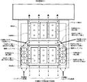
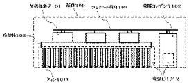
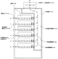
図5は、従来の半導体電力変換装置の冷却構造を示す平面図であり、図6はその正面図である。101は半導体素子、102は電解コンデンサ、103は冷却体、104は冷却風(半導体素子を通過)、105は冷却風(コンデンサを通過)、106は筐体、107はラミネート導体(絶縁積層導体)、108は筐体側風洞、109は背面側風洞、1010は風洞入口、1011はフィン、1012は吸気口である。 FIG. 5 is a plan view showing a cooling structure of a conventional semiconductor power converter, and FIG. 6 is a front view thereof. 101 is a semiconductor element, 102 is an electrolytic capacitor, 103 is a cooling body, 104 is cooling air (passing through the semiconductor element), 105 is cooling air (passing through the capacitor), 106 is a housing, 107 is a laminated conductor (insulating laminated conductor) , 108 is a housing side wind tunnel, 109 is a rear side wind tunnel, 1010 is a wind tunnel inlet, 1011 is a fin, and 1012 is an air inlet.
図5のとおり、筐体106には冷却体103が設置されている。冷却体103には半導体素子101が、後述する冷却風の流れに沿って取り付けられている。半導体素子101と並列して電解コンデンサ102が直列に配置されている。それらの上部にはラミネート導体107が設置されている。背面側には、風洞入口1010を有する筐体側風洞108と、背面側風洞109が形成されている。なお、筐体側風洞108は、半導体素子101や冷却体103側に通じている。
As shown in FIG. 5, a cooling body 103 is installed in the housing 106. The
そして、図6のとおり、冷却体103の底面側には放熱用のフィン1011が多数配列されている。筐体106の正面側には、吸気口1012が形成されており、ここから冷却風が筐体106内部へ導入される。 As shown in FIG. 6, a large number of heat dissipating fins 1011 are arranged on the bottom surface side of the cooling body 103. An intake port 1012 is formed on the front side of the housing 106, and cooling air is introduced into the housing 106 from here.
ここで、従来技術における冷却風の流れを説明する。
冷却風の流れは、図5中の矢印で示したとおりである。吸気口1012から流入した冷却風は大別して2通りの流路を辿る。半導体素子101を通過して冷却する冷却風104と、電解コンデンサ102を通過して冷却する冷却風105である。
Here, the flow of the cooling air in the prior art will be described.
The flow of the cooling air is as shown by the arrows in FIG. The cooling air flowing from the intake port 1012 is roughly divided and follows two flow paths. The cooling air 104 is cooled by passing through the
冷却風104は、半導体素子101を通過して冷却した後、筐体側風洞108へ入り、そこから背面側風洞109へと抜けて排気される。
冷却風105は、電解コンデンサ102を通過して冷却した後、風洞入口1010から筐体側風洞108へ入り、そこから冷却風104と同様に背面側風洞109へと抜けて排気される。
The cooling air 104 passes through the
The cooling air 105 passes through the electrolytic capacitor 102 and is cooled, and then enters the housing side wind tunnel 108 from the wind tunnel inlet 1010, and then passes through the back side wind tunnel 109 in the same manner as the cooling air 104 and is exhausted.
さらに、図7により、冷却風の排気されるまでの流れを示す。
図7は、従来の半導体電力変換装置の冷却構造を示す断面図である。1013は冷却ファン(排気用)、1014は本体部、1015は本体部の風洞、1016は本体部の吸気口である。
Further, FIG. 7 shows a flow until the cooling air is exhausted.
FIG. 7 is a cross-sectional view showing a cooling structure of a conventional semiconductor power conversion device. 1013 is a cooling fan (for exhaust), 1014 is a main body, 1015 is a wind tunnel of the main body, and 1016 is an air inlet of the main body.
本体部1014の内部には、各筐体106が縦方向に数段設けられている。また、本体部1014の正面側には本体部の吸気口1016、背面側には本体部の風洞1015が形成されている。本体部の風洞1015は背面側風洞109に通じている。 Inside the main body 1014, several cases 106 are provided in the vertical direction. Further, an air inlet 1016 of the main body portion is formed on the front side of the main body portion 1014, and a wind tunnel 1015 of the main body portion is formed on the back side. The wind tunnel 1015 of the main body portion communicates with the back side wind tunnel 109.
本体部の吸気口1016から流入した冷却風は、各筐体106の吸気口1012から筐体106内部へ入る。内部を通過した冷却風104と105は、合流して背面側風洞109を通り、本体部の風洞1015へ抜ける。そして、冷却ファン(排気用)1013により排出される。 Cooling air flowing from the air inlet 1016 of the main body enters the housing 106 through the air inlet 1012 of each housing 106. The cooling winds 104 and 105 that have passed through the interior merge and pass through the back side wind tunnel 109 and exit to the wind tunnel 1015 of the main body. Then, it is discharged by a cooling fan (for exhaust) 1013.
従来の半導体電力変換装置の冷却構造は以上である。 The cooling structure of the conventional semiconductor power converter is as described above.
このような従来の半導体電力変換装置の冷却構造には、以下のような課題があった。
冷却風104の風上から風下への方向に半導体素子101が配置されているため、冷却風104は風上の素子の発熱の影響を受け、風下の素子を冷却するときには温度が上昇しており、十分な冷却ができない。そのため、風下の素子を冷却するために冷却体103を大型化する必要があった。
Such a conventional cooling structure for a semiconductor power conversion device has the following problems.
Since the
また、半導体素子101を冷却する冷却風104と電解コンデンサ102を冷却する冷却風105を筐体側風洞108で合流させて排気しているため、筐体106および本体部1014も大型化する必要があった。
Further, since the cooling air 104 that cools the
このような装置の大型化はコストの増加につながってしまう。
さらに、そのような多量の風量を排気するためには、冷却ファン(排気用)1013も大型のものを使用せねばならず、騒音が大きくなるという問題もあった。
Such an increase in the size of the device leads to an increase in cost.
Further, in order to exhaust such a large amount of air, the cooling fan (exhaust) 1013 must be a large one, and there is a problem that noise increases.
そこで、本発明の目的は、上記の課題を解決するために、冷却能力を低下させることなく、半導体電力変換装置の小型化を実現することである。 Accordingly, an object of the present invention is to achieve downsizing of the semiconductor power conversion device without reducing the cooling capacity in order to solve the above-described problems.
前記の目的を達成するために、本発明によれば、複数の半導体素子および回路部品を筐体内に収納する半導体電力変換装置であって、前記筐体は、正面部に冷却風吸気部が形成されるとともに背面部に冷却風排気部が形成され、該冷却風吸気部から該冷却風排気部へ冷却風を強制通風することで内部を冷却するように構成されており、前記半導体素子は、通風方向に対して縦並びに配置され、前記回路部品は、風上側の前記半導体素子と横並びに配置され、前記筐体内部には、前記回路部品を冷却した冷却風と、風上側の前記半導体素子を冷却した冷却風とを合流させるチャンバを備え、前記チャンバは、風上から風下に向かって先細りの開口部を備え、前記チャンバの風下側には、風下側に位置付けられた前記半導体素子を冷却するガイド部が前記チャンバの幅狭の前記開口部から延長して配設されていることを特徴とする半導体電力変換装置とする。
In order to achieve the above object, according to the present invention, there is provided a semiconductor power conversion device for housing a plurality of semiconductor elements and circuit components in a housing, wherein the housing is formed with a cooling air intake portion at a front portion. In addition, a cooling air exhaust part is formed on the back surface, and the cooling element is configured to cool the inside by forcibly passing cooling air from the cooling air intake part to the cooling air exhaust part. Arranged vertically and in the direction of ventilation, the circuit component is arranged side by side with the semiconductor element on the windward side, and inside the housing, cooling air for cooling the circuit component and the semiconductor element on the windward side A chamber that joins the cooling air that has cooled the chamber, the chamber having an opening that tapers from the windward to the leeward, and cools the semiconductor element positioned on the leeward side on the leeward side of the chamber. To guide There is a semiconductor power conversion device which is characterized that you have been provided extending from narrow the opening of the chamber.
また、本発明によれば、上記の構成において、前記回路部品の近傍には、前記回路部品を冷却した冷却風を前記チャンバに案内する冷却風ガイド板が配設されていることを特徴とする半導体電力変換装置とする。 According to the present invention, in the above configuration, a cooling air guide plate that guides cooling air that has cooled the circuit component to the chamber is disposed in the vicinity of the circuit component. A semiconductor power converter is assumed.
また、本発明によれば、上記の構成において、前記回路部品の発熱量が、風上側の前記半導体素子の発熱量よりも少ないことを特徴とする半導体電力変換装置とする。
また、本発明によれば、上記の構成において、前記回路部品を冷却した冷却風は、風上側の前記半導体素子を冷却した冷却風よりも低い温度であることを特徴とする半導体電力変換装置とする
In addition, according to the present invention, in the above configuration, the semiconductor power conversion device is characterized in that the heat generation amount of the circuit component is smaller than the heat generation amount of the semiconductor element on the windward side .
According to the present invention, in the above configuration, the cooling air that has cooled the circuit component is lower in temperature than the cooling air that has cooled the semiconductor element on the windward side. Do
本発明により、冷却能力を低下させることなく、半導体電力変換装置の小型化を実現することができる。 By this invention, size reduction of a semiconductor power converter device is realizable, without reducing cooling capacity.
実施の形態を以下の実施例で説明する。 Embodiments will be described in the following examples.
図1ないし3により、本発明の実施例1を説明する。
最初に、図1および2により、実施例1の筐体部分の構成を説明する。
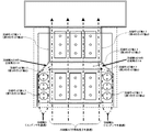
図1は、本発明の実施例1の半導体電力変換装置の冷却構造を示す平面図であり、図2はその正面図である。1は半導体素子、2は電解コンデンサ(回路部品)、3は冷却体、4は冷却風(半導体素子を冷却)、5は冷却風(コンデンサを冷却)、6は筐体、7はラミネート導体(絶縁積層導体)、9は背面側風洞、10は風洞入口、11はフィン、12は吸気口、17は冷却ガイド板(a〜c)、18は冷却風4と5の合流地点である。
A first embodiment of the present invention will be described with reference to FIGS.
First, referring to FIGS. 1 and 2, the configuration of the housing portion of the first embodiment will be described.
1 is a plan view showing a cooling structure of a semiconductor power conversion device according to a first embodiment of the present invention, and FIG. 2 is a front view thereof. 1 is a semiconductor element, 2 is an electrolytic capacitor (circuit component), 3 is a cooling body, 4 is cooling air (cooling the semiconductor element), 5 is cooling air (cooling the capacitor), 6 is a housing, 7 is a laminated conductor ( Insulated laminated conductor), 9 is a rear side wind tunnel, 10 is a wind tunnel inlet, 11 is a fin, 12 is an air inlet, 17 is a cooling guide plate (ac), 18 is a meeting point of the
ここで、冷却ガイド板17の第2のガイド板bおよび第3のガイド板cによりチャンバが構成される。なお、第1のガイド板aは、回路部品を冷却した冷却風を前記チャンバに案内する機能を有する。また、回路部品とは、半導体素子以外の電気部品であり、例えば、発熱量を持つコンデンサなどがそれに相当する。本実施例では、電解コンデンサとしている。 Here, the second guide plate b and the third guide plate c of the cooling guide plate 17 constitute a chamber. The first guide plate a has a function of guiding the cooling air that has cooled the circuit components to the chamber. Further, the circuit component is an electrical component other than the semiconductor element, and for example, a capacitor having a heat generation amount corresponds to the circuit component. In this embodiment, an electrolytic capacitor is used.
図1および2のとおり、筐体6の内部には、冷却風4の風向きに沿って、風上側に3個の半導体素子1が並列で配置されており、風下側にも3個の半導体素子1が並列で配置されている。そして、それらの正面側の半導体素子1を挟むように、冷却風5の風向きに沿って、電解コンデンサ2の3個ずつ直列の配列が2列配置されている。
As shown in FIGS. 1 and 2, three
半導体素子1には、風上側と風下側のそれぞれに別々の冷却体3が取り付けられている。冷却体3には、半導体素子1の取付面とは反対の面にフィン11が形成されている。なお、半導体素子1と電解コンデンサ2は、ラミネート導体7で覆われている。
正面側には、吸気口12が形成され、ここから、冷却風4および5が流入する。そして、半導体素子1および電解コンデンサ2を冷却して、筐体6の後方の背面側風洞9へ抜けて排気される。
An
ここで、筐体6には、冷却ガイド板17が設置されている。冷却ガイド板17は第1〜3のガイド板a〜cより構成されている。
第1のガイド板aは、2列の直列の電解コンデンサ2と並行するように電解コンデンサ2の外側にそれぞれ形成されている。
Here, a cooling guide plate 17 is installed in the housing 6. The cooling guide plate 17 is composed of first to third guide plates a to c.
The first guide plates a are respectively formed outside the electrolytic capacitors 2 so as to be parallel to the two rows of series electrolytic capacitors 2.
第2のガイド板bは、それぞれの第1のガイド板aの背面側の端部から内側へ向けて斜め方向に形成されている。
第3のガイド板cは、両側の第2のガイド板b同士を結び、平面側からは台形状となるように形成されている。正面側からは両側の第2のガイド板bの背面側の端部同士を結んで形成されているが、背面側の半導体素子1を覆うように形成されている。
The second guide plate b is formed in an oblique direction from the back side end of each first guide plate a toward the inside.
The third guide plate c connects the second guide plates b on both sides and is formed in a trapezoidal shape from the plane side. From the front side, the back end portions of the second guide plates b on both sides are connected to each other, but are formed so as to cover the
つまり、冷却ガイド板17の第2のガイド板bおよび第3のガイド板cから構成されるチャンバは、通風方向の風上から風下に向かって先細りの開口部を備えることになる。
実施例1の筐体部分の構成の説明は以上である。
That is, the chamber constituted by the second guide plate b and the third guide plate c of the cooling guide plate 17 has an opening that tapers from the windward side in the ventilation direction toward the leeward side.
This is the end of the description of the configuration of the housing portion of the first embodiment.
次に、図3により、実施例1の本体部分の構成を説明する。
図3は、本発明の実施例1の半導体電力変換装置の冷却構造を示す断面図である。13は冷却ファン(排気用)、14は本体部、15は本体部の風洞、16は本体部の吸気口である。
Next, the configuration of the main body portion of the first embodiment will be described with reference to FIG.
FIG. 3 is a cross-sectional view illustrating the cooling structure of the semiconductor power conversion device according to the first embodiment of the present invention. 13 is a cooling fan (for exhaust), 14 is a main body, 15 is a wind tunnel of the main body, and 16 is an air inlet of the main body.
図3のとおり、本体部14の内部で、筐体6は多数段並べて収納されている。本体部の吸気口16と各筐体6の吸気口12とは通じている。さらに各筐体6は、後方に形成された背面側風洞9を通して、本体部の風洞15通じており、本体部の風洞15には冷却ファン(排気用)13が設置されている。
As shown in FIG. 3, the housing 6 is housed in a large number of stages inside the main body 14. The air inlet 16 of the main body and the
実施例1の本体部分の構成の説明は以上である。
続いて、図1ないし3により、実施例1の動作を説明する。
図3のとおり、本体部の吸気口16から流入した冷却風は、各筐体6の吸気口12より筐体6内部へ流入する。このとき、冷却風は、冷却風4(半導体素子を冷却)および冷却風5(コンデンサを冷却)として内部へ流入する。
This is the end of the description of the configuration of the main body portion of the first embodiment.
Subsequently, the operation of the first embodiment will be described with reference to FIGS.
As shown in FIG. 3, the cooling air flowing from the air inlet 16 of the main body flows into the housing 6 from the
先ず、冷却風4は、風上側の半導体素子1を冷却するが、半導体素子1は風上側と風下側とでそれぞれ別々の冷却体3に取り付けられているため、冷却風4の流入により、それぞれの冷却体3で冷却効果を発揮する。
First, the cooling wind 4 cools the
一方、両側の冷却風5は、それぞれ電解コンデンサ2を冷却する。このとき、電解コンデンサ2の外側は第1のガイド板aで覆われている。さらに電解コンデンサ2の前方も第2のガイド板bで覆われている。このため、冷却風5は、電解コンデンサ2を冷却した後、風上側の半導体素子1と風下側の半導体素子1との間に流入することになる。
On the other hand, the cooling
そのため、風上側の半導体素子1を通過した冷却風4と冷却風5とが、冷却風4と5の合流地点18で合流することになる。さらに、第3のガイド板cにより、合流地点18の平面側および背面側が覆われているため、効率よく合流される。
Therefore, the cooling air 4 and the cooling
なお、電解コンデンサ2は、半導体素子1に比べて発熱量が非常に少ないため、冷却風5(電解コンデンサを冷却)の温度は、冷却風4(風上側の半導体素子を冷却)よりも低い温度となっている。
Since the electrolytic capacitor 2 generates much less heat than the
従って、合流地点18において、冷却風4に対して、温度の低い冷却風5を合流させることにより、風下側の半導体素子1へ流入する手前で、冷却風4の温度上昇を抑制することができる。
Therefore, the temperature rise of the cooling air 4 can be suppressed before flowing into the
さらに、第3のガイド板cが合流地点18の背面側(風下の半導体素子1の正面側)を覆っているため(図2)、合流地点18で合流した冷却風4および5は、風下側の半導体素子1に直接当たるのではなく、冷却体3およびフィン11に直接当たることになる。これにより、風下側の半導体素子1の冷却効率の向上を図ることができる。
Further, since the third guide plate c covers the back side of the joining point 18 (the front side of the leeward semiconductor element 1) (FIG. 2), the cooling winds 4 and 5 joined at the joining
このように、合流地点18で合流した冷却風4および5は、風下側の半導体素子1を冷却した後、背面側風洞9へ抜ける。
その後、図3のとおり、各背面側風洞9からの通風は、本体部の風洞15を通って、冷却ファン(排気用)13により外部へ排出される。
In this way, the cooling winds 4 and 5 merged at the
After that, as shown in FIG. 3, the ventilation from each rear side wind tunnel 9 passes through the wind tunnel 15 of the main body and is discharged to the outside by a cooling fan (for exhaust) 13.
実施例1の動作は以上である。
かくして本発明の実施例1によれば、冷却ガイド板17が設けられていることにより、合流地点18で冷却風4と温度の低い冷却風5とを合流させることができる。これにより、風下側の半導体素子1へ流入する手前で、風上側の半導体素子の発熱による冷却風の温度上昇を抑制することができる。そのため、風下側の半導体素子1が、風上側の半導体素子1の発熱の影響を受けることなく、冷却効率を向上させることができる。従って、冷却体3を大型化する必要がなく、小型化することができる。
The operation of the first embodiment is as described above.
Thus, according to the first embodiment of the present invention, the cooling guide plate 17 is provided, so that the cooling air 4 and the cooling
また、電解コンデンサ2の冷却についても、従来のように複数個を直列に配置していた場合には、風下側の電解コンデンサ2に到達する冷却風の温度は上昇してしまっていた。しかし、電解コンデンサ2を分離して配置することにより、電解コンデンサ2を効率良く冷却することができるため、電解コンデンサを小型化することができる。 Further, regarding the cooling of the electrolytic capacitor 2, when a plurality of the electrolytic capacitors 2 are arranged in series as in the prior art, the temperature of the cooling air reaching the leeward electrolytic capacitor 2 has increased. However, since the electrolytic capacitor 2 can be cooled efficiently by separating and arranging the electrolytic capacitor 2, the electrolytic capacitor can be reduced in size.
さらに、合流地点18で冷却風を合流させているため、冷却に必要な風量を全体的に低減することができる。そのため、冷却ファン13(排気用)を小型化することができ、騒音を抑えることができる。
Furthermore, since the cooling air is merged at the
そのほか、従来、半導体素子を通過した冷却風と電解コンデンサを通過した冷却風とを合わせて排気するために筐体側風洞を設置していたが、これを不要とすることができるため、筐体6の小型化を図ることができる。 In addition, conventionally, a case-side wind tunnel has been installed to exhaust the cooling air that has passed through the semiconductor element and the cooling air that has passed through the electrolytic capacitor. Can be miniaturized.
このように、全体的にユニットの寸法を小型化できるため、半導体電力変換装置全体の小型化が実現でき、設置スペースを縮小することができる。
続いて、図4により、本発明の実施例2を説明する。
Thus, since the size of the unit can be reduced as a whole, the entire semiconductor power conversion device can be reduced in size, and the installation space can be reduced.
Subsequently, Embodiment 2 of the present invention will be described with reference to FIG.
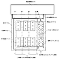
図4は、本発明の実施例2の半導体電力変換装置の冷却構造を示す平面図である。冷却ガイド板17は、第1〜4のガイド板a〜dより構成されている。ここで、第4のガイド板dが、風下側に位置付けられた半導体素子1を冷却するガイド部となる。
FIG. 4 is a plan view showing a cooling structure of the semiconductor power conversion device according to the second embodiment of the present invention. The cooling guide plate 17 includes first to fourth guide plates a to d. Here, the fourth guide plate d serves as a guide part for cooling the
なお、実施例2の説明では、実施例1と同じ部分についてはその詳細な説明を省略し、異なる点を中心に説明を行う。
実施例2の構成を図4により説明する。
In the description of the second embodiment, detailed description of the same parts as those in the first embodiment will be omitted, and different points will be mainly described.
The configuration of the second embodiment will be described with reference to FIG.
図4のとおり、半導体素子1や電解コンデンサ2等の構成は実施例1と同じである。異なる点は、冷却ガイド板17の構成である。
ここでは、冷却ガイド板17には、第1〜3のガイド板a〜cに加えて、第4のガイド板dが形成されている。
As shown in FIG. 4, the configuration of the
Here, in addition to the first to third guide plates a to c, a fourth guide plate d is formed on the cooling guide plate 17.
第4のガイド板dは、第3のガイド板cの背面側の端部より筐体の背面まで延びている。これにより、風下側の半導体素子1および冷却体3、フィン11の両側を遮蔽して、通風路を形成している。
The fourth guide plate d extends from the back side end of the third guide plate c to the back of the housing. Thereby, the
つまり、風下側に位置付けられた半導体素子1を冷却するガイド部である第4のガイド板dは、チャンバ(冷却ガイド板17の第2のガイド板bおよび第3のガイド板c)の幅狭の開口部から延長して配設されている。
That is, the fourth guide plate d, which is a guide portion for cooling the
実施例2の構成の説明は以上である。
続いて、実施例2の動作を説明する。
実施例1と同様に、吸気口12から筐体6内部へ流入した冷却風4および5は、合流地点18で合流し、さらに風下側の半導体素子1に取り付けられた冷却体3およびフィン11へ向かう。
This is the end of the description of the configuration of the second embodiment.
Subsequently, the operation of the second embodiment will be described.
As in the first embodiment, the cooling winds 4 and 5 flowing into the housing 6 from the
ここで、実施例2では、さらに第4のガイド板dにより、風下側の半導体素子1および冷却体3、フィン11の両側を遮蔽して、通風路が形成されているため、合流地点18から流入した冷却風が拡散することなく、風下側の半導体素子1を効率よく冷却することができる。
Here, in Example 2, the fourth guide plate d further shields both sides of the
なお、ガイド部として実施例2では第4のガイド板dを使用したが、これに限定されるものではなく、筒状や矩形状のものでもよい。
実施例2の動作は以上である。
In the second embodiment, the fourth guide plate d is used as the guide portion. However, the guide portion is not limited to this, and may be cylindrical or rectangular.
The operation of the second embodiment is as described above.
かくして本発明の実施例2によれば、冷却ガイド板17に第4のガイド板dが設置されていることにより、風下側の半導体素子1の冷却効果をさらに向上させることができる。従って、冷却体3を大型化する必要がなく、小型化することができる。また、冷却ファン13(排気用)を小型化することができ、騒音を抑えることができる。このように、全体的にユニットの寸法を小型化できるため、半導体電力変換装置全体の小型化が実現でき、設置スペースを縮小することができる。
Thus, according to the second embodiment of the present invention, the cooling effect of the
なお、上記実施形態は好ましい実施例について述べたものであり、本発明の趣旨を逸脱することなく、種々の変形実施例が可能なことは勿論である。即ち、冷却ガイド板や半導体素子、電解コンデンサ、冷却体等の寸法や各部分の形状等は、設置現場の要求および状況等に応じて種々変更されるべきものである。 In addition, the said embodiment described the preferable Example, Of course, a various deformation | transformation Example is possible, without deviating from the meaning of this invention. That is, the dimensions of the cooling guide plate, the semiconductor element, the electrolytic capacitor, the cooling body, the shape of each part, and the like should be variously changed according to the requirements and circumstances of the installation site.
1 半導体素子
2 電解コンデンサ(回路部品)
3 冷却体
4 冷却風(半導体素子を冷却)
5 冷却風(コンデンサを冷却)
6 筐体
7 ラミネート導体(絶縁積層導体)
8 筐体側風洞
9 背面側風洞
10 風洞入口
11 フィン
12 吸気口
13 冷却ファン(排気用)
14 本体部
15 本体部の風洞
16 本体部の吸気口
17 冷却ガイド板
17a 第1のガイド板
17b 第2のガイド板(チャンバ)
17c 第3のガイド板(チャンバ)
17d 第4のガイド板(ガイド部)
18 冷却風4と5の合流地点
1 Semiconductor element 2 Electrolytic capacitor (circuit parts)
3 Cooling body 4 Cooling air (cools the semiconductor element)
5 Cooling air (cools the condenser)
6 Housing 7 Laminated conductor (insulated laminated conductor)
8 Housing side wind tunnel 9 Back side wind tunnel 10 Wind tunnel inlet 11
14 Body portion 15 Air channel 16 of body portion Air intake port 17 of body portion Cooling guide plate 17a First guide plate 17b Second guide plate (chamber)
17c Third guide plate (chamber)
17d Fourth guide plate (guide portion)
18 Confluence of cooling
Claims (4)
前記筐体は、正面部に冷却風吸気部が形成されるとともに背面部に冷却風排気部が形成され、該冷却風吸気部から該冷却風排気部へ冷却風を強制通風することで内部を冷却するように構成されており、
前記半導体素子は、通風方向に対して縦並びに配置され、
前記回路部品は、風上側の前記半導体素子と横並びに配置され、
前記筐体内部には、前記回路部品を冷却した冷却風と、風上側の前記半導体素子を冷却した冷却風とを合流させるチャンバを備え、
前記チャンバは、風上から風下に向かって先細りの開口部を備え、
前記チャンバの風下側には、風下側に位置付けられた前記半導体素子を冷却するガイド部が前記チャンバの幅狭の前記開口部から延長して配設されていることを特徴とする半導体電力変換装置。 A semiconductor power conversion device that houses a plurality of semiconductor elements and circuit components in a housing,
The casing has a cooling air intake portion formed in the front portion and a cooling air exhaust portion formed in the back portion, and the cooling air is forcibly ventilated from the cooling air intake portion to the cooling air exhaust portion. Configured to cool,
The semiconductor elements are arranged vertically with respect to the ventilation direction,
The circuit component is arranged side by side with the semiconductor element on the windward side,
The housing includes a chamber for combining cooling air that has cooled the circuit components and cooling air that has cooled the semiconductor element on the windward side ,
The chamber includes an opening that tapers from the windward to the windward,
Downwind of said chamber, a semiconductor power conversion device which is characterized that you have been provided guide portion for cooling the semiconductor device positioned on the leeward side extending from narrow the opening of the chamber .
前記回路部品の近傍には、前記回路部品を冷却した冷却風を前記チャンバに案内する冷却風ガイド板が配設されていることを特徴とする半導体電力変換装置。 The semiconductor power conversion device according to claim 1,
In the vicinity of the circuit component, a cooling air guide plate for guiding the cooling air that has cooled the circuit component to the chamber is disposed.
前記回路部品の発熱量が、風上側の前記半導体素子の発熱量よりも少ないことを特徴とする半導体電力変換装置。 The semiconductor power conversion device according to claim 1 ,
A semiconductor power conversion device characterized in that a heat generation amount of the circuit component is smaller than a heat generation amount of the semiconductor element on the windward side .
前記回路部品を冷却した冷却風は、風上側の前記半導体素子を冷却した冷却風よりも低い温度であることを特徴とする半導体電力変換装置。
The semiconductor power conversion device according to claim 1 ,
The semiconductor power conversion device according to claim 1 , wherein the cooling air that has cooled the circuit components is at a lower temperature than the cooling air that has cooled the semiconductor element on the windward side .
Priority Applications (1)
| Application Number | Priority Date | Filing Date | Title |
|---|---|---|---|
| JP2011049077A JP5691663B2 (en) | 2011-03-07 | 2011-03-07 | Semiconductor power converter cooling structure |
Applications Claiming Priority (1)
| Application Number | Priority Date | Filing Date | Title |
|---|---|---|---|
| JP2011049077A JP5691663B2 (en) | 2011-03-07 | 2011-03-07 | Semiconductor power converter cooling structure |
Publications (2)
| Publication Number | Publication Date |
|---|---|
| JP2012186352A JP2012186352A (en) | 2012-09-27 |
| JP5691663B2 true JP5691663B2 (en) | 2015-04-01 |
Family
ID=47016140
Family Applications (1)
| Application Number | Title | Priority Date | Filing Date |
|---|---|---|---|
| JP2011049077A Active JP5691663B2 (en) | 2011-03-07 | 2011-03-07 | Semiconductor power converter cooling structure |
Country Status (1)
| Country | Link |
|---|---|
| JP (1) | JP5691663B2 (en) |
Families Citing this family (7)
| Publication number | Priority date | Publication date | Assignee | Title |
|---|---|---|---|---|
| JP6354278B2 (en) * | 2014-04-15 | 2018-07-11 | 富士電機株式会社 | Semiconductor power converter |
| JP6300363B2 (en) * | 2014-07-03 | 2018-03-28 | 株式会社日立製作所 | Power converter |
| JP6166743B2 (en) * | 2015-02-20 | 2017-07-19 | 本田技研工業株式会社 | Power converter |
| JP6610193B2 (en) * | 2015-11-18 | 2019-11-27 | 富士電機株式会社 | Power converter |
| JP6728667B2 (en) * | 2015-12-15 | 2020-07-22 | 富士電機株式会社 | Cooling device and power conversion device |
| JP7485855B1 (en) * | 2022-06-17 | 2024-05-16 | 株式会社Tmeic | Power Conversion Unit |
| JP7511772B1 (en) * | 2023-02-22 | 2024-07-05 | 株式会社Tmeic | Power Conversion Unit |
Family Cites Families (5)
| Publication number | Priority date | Publication date | Assignee | Title |
|---|---|---|---|---|
| JPS57191088U (en) * | 1981-05-29 | 1982-12-03 | ||
| JPS60192497U (en) * | 1984-05-31 | 1985-12-20 | 富士通株式会社 | cooling structure |
| JPH03155696A (en) * | 1989-08-31 | 1991-07-03 | Fuji Electric Co Ltd | Electric power conversion apparatus and smoothing capacitor mounting device |
| JP2007184464A (en) * | 2006-01-10 | 2007-07-19 | Toshiba Corp | Railway vehicle control system |
| JP2008078423A (en) * | 2006-09-21 | 2008-04-03 | Fuji Electric Systems Co Ltd | Semiconductor power converter cooling structure |
-
2011
- 2011-03-07 JP JP2011049077A patent/JP5691663B2/en active Active
Also Published As
| Publication number | Publication date |
|---|---|
| JP2012186352A (en) | 2012-09-27 |
Similar Documents
| Publication | Publication Date | Title |
|---|---|---|
| JP5691663B2 (en) | Semiconductor power converter cooling structure | |
| CN104662372B (en) | The outdoor unit of air conditioner | |
| JP5488565B2 (en) | Power converter | |
| CN102404979B (en) | Electronic device | |
| JP5794101B2 (en) | Forced air cooling heat sink | |
| CN106059257A (en) | Cooled power conversion assembly | |
| JP5554651B2 (en) | Power converter | |
| JP5704760B2 (en) | Quick charger | |
| JP2008103576A (en) | Motor control device | |
| JP6094416B2 (en) | Power converter | |
| CN106169875B (en) | Semiconductor power conversion device | |
| CN216357975U (en) | Photovoltaic inverter | |
| JP6074346B2 (en) | Switchboard equipment | |
| JP6248277B2 (en) | Power converter | |
| JP5787105B2 (en) | Power converter | |
| JP2010147131A (en) | Power conversion apparatus | |
| JP4360123B2 (en) | Power converter | |
| JP6115430B2 (en) | Power converter | |
| CN203747673U (en) | Electric power conversion device | |
| JP6841734B2 (en) | Electrical equipment | |
| JP6728667B2 (en) | Cooling device and power conversion device | |
| US11879648B2 (en) | Outdoor machine and air conditioner | |
| JP6575914B2 (en) | Power converter | |
| JP6268361B2 (en) | Inverter device | |
| JP2023097547A (en) | Capacitor cooling structure and power conversion device |
Legal Events
| Date | Code | Title | Description |
|---|---|---|---|
| A621 | Written request for application examination |
Free format text: JAPANESE INTERMEDIATE CODE: A621 Effective date: 20140214 |
|
| A977 | Report on retrieval |
Free format text: JAPANESE INTERMEDIATE CODE: A971007 Effective date: 20140930 |
|
| A131 | Notification of reasons for refusal |
Free format text: JAPANESE INTERMEDIATE CODE: A131 Effective date: 20141104 |
|
| A521 | Request for written amendment filed |
Free format text: JAPANESE INTERMEDIATE CODE: A523 Effective date: 20141204 |
|
| TRDD | Decision of grant or rejection written | ||
| A01 | Written decision to grant a patent or to grant a registration (utility model) |
Free format text: JAPANESE INTERMEDIATE CODE: A01 Effective date: 20150106 |
|
| A61 | First payment of annual fees (during grant procedure) |
Free format text: JAPANESE INTERMEDIATE CODE: A61 Effective date: 20150119 |
|
| R150 | Certificate of patent or registration of utility model |
Ref document number: 5691663 Country of ref document: JP Free format text: JAPANESE INTERMEDIATE CODE: R150 |
|
| R250 | Receipt of annual fees |
Free format text: JAPANESE INTERMEDIATE CODE: R250 |
|
| R250 | Receipt of annual fees |
Free format text: JAPANESE INTERMEDIATE CODE: R250 |
|
| R250 | Receipt of annual fees |
Free format text: JAPANESE INTERMEDIATE CODE: R250 |
|
| R250 | Receipt of annual fees |
Free format text: JAPANESE INTERMEDIATE CODE: R250 |
|
| R250 | Receipt of annual fees |
Free format text: JAPANESE INTERMEDIATE CODE: R250 |
|
| R250 | Receipt of annual fees |
Free format text: JAPANESE INTERMEDIATE CODE: R250 |
|
| R250 | Receipt of annual fees |
Free format text: JAPANESE INTERMEDIATE CODE: R250 |
|
| R250 | Receipt of annual fees |
Free format text: JAPANESE INTERMEDIATE CODE: R250 |
|
| R250 | Receipt of annual fees |
Free format text: JAPANESE INTERMEDIATE CODE: R250 |