JP5674871B2 - Inductively coupled plasma processing equipment - Google Patents
Inductively coupled plasma processing equipment Download PDFInfo
- Publication number
- JP5674871B2 JP5674871B2 JP2013146049A JP2013146049A JP5674871B2 JP 5674871 B2 JP5674871 B2 JP 5674871B2 JP 2013146049 A JP2013146049 A JP 2013146049A JP 2013146049 A JP2013146049 A JP 2013146049A JP 5674871 B2 JP5674871 B2 JP 5674871B2
- Authority
- JP
- Japan
- Prior art keywords
- antenna
- impedance
- inductively coupled
- processing chamber
- plasma processing
- Prior art date
- Legal status (The legal status is an assumption and is not a legal conclusion. Google has not performed a legal analysis and makes no representation as to the accuracy of the status listed.)
- Active
Links
Images


Description
本発明は、液晶表示装置(LCD)等のフラットパネルディスプレイ(FPD)製造用の基板等の被処理体にプラズマ処理を施す誘導結合プラズマ処理装置に関する。 The present invention relates to an inductively coupled plasma processing apparatus for performing plasma processing on a target object such as a substrate for manufacturing a flat panel display (FPD) such as a liquid crystal display (LCD).
液晶表示装置(LCD)等の製造工程においては、ガラス基板に所定の処理を施すために、プラズマエッチング装置やプラズマCVD成膜装置等の種々のプラズマ処理装置が用いられる。このようなプラズマ処理装置としては従来、容量結合プラズマ処理装置が多用されていたが、近時、高真空度で高密度のプラズマを得ることができるという大きな利点を有する誘導結合プラズマ(Inductively Coupled Plasma:ICP)処理装置が注目されている。 In a manufacturing process of a liquid crystal display (LCD) or the like, various plasma processing apparatuses such as a plasma etching apparatus and a plasma CVD film forming apparatus are used to perform a predetermined process on a glass substrate. Conventionally, a capacitively coupled plasma processing apparatus has been widely used as such a plasma processing apparatus. Recently, however, an inductively coupled plasma (Inductively Coupled Plasma) having a great advantage that a high-density plasma can be obtained at a high vacuum degree. : ICP) processing devices are attracting attention.
誘導結合プラズマ処理装置は、被処理体を収容する処理容器の誘電体窓の外側に高周波アンテナを配置し、処理容器内に処理ガスを供給するとともにこの高周波アンテナに高周波電力を供給することにより、処理容器内に誘導結合プラズマを生じさせ、この誘導結合プラズマによって被処理体に所定のプラズマ処理を施すものである。誘導結合プラズマ処理装置の高周波アンテナとしては、平面状の所定パターンをなす平面アンテナが多用されている。 The inductively coupled plasma processing apparatus arranges a high frequency antenna outside a dielectric window of a processing container that accommodates an object to be processed, supplies a processing gas into the processing container and supplies high frequency power to the high frequency antenna. Inductively coupled plasma is generated in the processing container, and the object to be processed is subjected to a predetermined plasma treatment by the inductively coupled plasma. As a high-frequency antenna for an inductively coupled plasma processing apparatus, a planar antenna having a predetermined planar pattern is often used.
このような、平面アンテナを用いた誘導結合プラズマ処理装置では、処理容器内の平面アンテナ直下の空間にプラズマが生成されるが、その際に、アンテナ直下の各位置での電界強度に比例して高プラズマ密度領域と低プラズマ領域の分布を持つことから、平面アンテナのパターン形状がプラズマ密度分布を決める重要なファクターとなっている。 In such an inductively coupled plasma processing apparatus using a planar antenna, plasma is generated in a space immediately below the planar antenna in the processing container. At that time, the plasma is generated in proportion to the electric field strength at each position immediately below the antenna. Due to the distribution of the high plasma density region and the low plasma region, the pattern shape of the planar antenna is an important factor that determines the plasma density distribution.
ところで、一台の誘導結合プラズマ処理装置が対応すべきアプリケーションは一つとは限らず、複数のアプリケーションに対応する必要がある。その場合には、それぞれのアプリケーションにおいて均一な処理を行うためにプラズマ密度分布を変化させる必要があり、そのために高密度領域および低密度領域の位置を異ならせるように異なる形状のアンテナを複数準備してアプリケーションに応じてアンテナを取り替えることが行われている。 By the way, the number of applications that a single inductively coupled plasma processing apparatus should support is not limited to one, and it is necessary to support a plurality of applications. In that case, it is necessary to change the plasma density distribution in order to perform uniform processing in each application.To that end, multiple antennas with different shapes are prepared so that the positions of the high-density region and low-density region are different. The antenna is replaced according to the application.
しかしながら、複数のアプリケーションに対応して複数のアンテナを準備し、異なるアプリケーションごとに交換することは非常に多くの労力を要し、また、近時、LCD用のガラス基板が大型化していることからアンテナ製造費用も高価なものとなっている。また、このように複数のアンテナを用意したとしても、与えられたアプリケーションにおいて必ずしも最適条件とは限らず、プロセス条件の調整により対応せざるを得ない。 However, preparing a plurality of antennas corresponding to a plurality of applications and exchanging them for each different application requires a great deal of labor, and recently, the glass substrate for LCD is becoming larger. Antenna manufacturing costs are also expensive. Further, even if a plurality of antennas are prepared in this way, the given application is not necessarily the optimum condition, and must be dealt with by adjusting process conditions.
これに対して、特許文献1には、渦巻き形アンテナを内側部分と外側部分の2つに分割して設け、少なくとも一方のアンテナ部分に可変コンデンサ等のインピーダンス調節手段を設け、これによるインピーダンス調節により、上記2つのアンテナ部分の電流値を制御し、処理室内に形成される誘導結合プラズマの密度分布を制御する技術が開示されている。 On the other hand, in Patent Document 1, a spiral antenna is divided into two parts, an inner part and an outer part, and impedance adjusting means such as a variable capacitor is provided in at least one of the antenna parts. A technique for controlling the current values of the two antenna portions to control the density distribution of inductively coupled plasma formed in the processing chamber is disclosed.
上記特許文献1の技術では、渦巻き形アンテナの内側部分と外側部分の直下にアンテナによって形成される電界に対応した強度のプラズマが形成されるがプラズマが水平方向に拡散することにより、プラズマ密度分布を均一に制御可能である。しかしながら、基板の1辺の長さが1mを超えて大型化した場合には、このような拡散効果が十分に発揮されず、アンテナパターン密、疎の分布が反映されやすくなることからプラズマ分布が悪化する傾向となる。また、このように基板が大型化するとアンテナ配置領域において電界強度分布に差が生じてしまい、それによってもプラズマ分布が不均一となってしまう。 In the technique of the above-mentioned Patent Document 1, plasma having an intensity corresponding to the electric field formed by the antenna is formed immediately below the inner part and the outer part of the spiral antenna. Can be controlled uniformly. However, when the length of one side of the substrate exceeds 1 m, the diffusion effect is not sufficiently exhibited, and the antenna pattern dense and sparse distribution is easily reflected. It tends to get worse. In addition, when the substrate is increased in size as described above, a difference occurs in the electric field intensity distribution in the antenna arrangement region, which also causes the plasma distribution to be non-uniform.
本発明はかかる事情に鑑みてなされたものであって、大型基板に対しても、均一なプラズマ分布を得ることができる誘導結合プラズマ処理装置を提供することを課題とする。 This invention is made | formed in view of this situation, Comprising: It aims at providing the inductively coupled plasma processing apparatus which can obtain uniform plasma distribution also with respect to a large sized substrate.
上記課題を解決するため、本発明は、矩形状の被処理体を収容してプラズマ処理を施す処理室と、前記処理室内で被処理体が載置される載置台と、前記処理室内に処理ガスを供給する処理ガス供給系と、前記処理室内を排気する排気系と、前記処理室の外部に誘電体部材を介して配置され、高周波電力が供給されることにより前記処理室内に誘導電界を形成する同心状に設けられた3以上のアンテナ部を有する高周波アンテナと、前記各アンテナ部を含むアンテナ回路のうち少なくとも一つのインピーダンスを調節し、これにより前記アンテナ部の電流値を制御するインピーダンス調節手段とを具備し、前記各アンテナ部は、該アンテナ部自体が略矩形状になるように複数のアンテナ線が渦巻き状に配置されてなる多重アンテナを構成し、かつその配置領域において均一な電界が形成されるようにその巻き方が設定され、各アンテナ部の配置領域間で電界の均一化が可能なように、内側のアンテナ部から外側のアンテナ部に向かって、前記各アンテナ部の各辺の中央部において巻き数が少なくなるように各アンテナ線の巻き数が設定されることを特徴とする誘導結合プラズマ処理装置を提供する。 In order to solve the above problems, the present invention provides a processing chamber that accommodates a rectangular object to be processed and performs plasma processing, a mounting table on which the object to be processed is mounted, and a process in the processing chamber. A processing gas supply system for supplying gas, an exhaust system for exhausting the processing chamber, and a dielectric member disposed outside the processing chamber, and by supplying high frequency power, an induction electric field is generated in the processing chamber. Impedance adjustment for adjusting the impedance of at least one of a high frequency antenna having three or more antenna portions provided concentrically to be formed and an antenna circuit including the antenna portions, thereby controlling a current value of the antenna portion Each antenna unit constitutes a multiple antenna in which a plurality of antenna wires are spirally arranged so that the antenna unit itself has a substantially rectangular shape. As the winding as a uniform electric field is formed in the arrangement region is set, to allow uniform electric field between arrangement region of each antenna unit, from the inside toward the antenna section on the outside of the antenna portion The inductively coupled plasma processing apparatus is characterized in that the number of turns of each antenna wire is set so that the number of turns is reduced in the central part of each side of each antenna part .
本発明において、前記インピーダンス調節手段は、前記各アンテナ部を含むアンテナ回路のうち少なくとも一つに接続され、その接続されたアンテナ回路のインピーダンスを調節する構成とすることができる。この場合に、前記インピーダンス調節手段は、可変コンデンサを有するものとすることができる。また、アプリケーションごとに最適なプラズマ密度分布が得られる前記インピーダンス調節手段の調節パラメータが予め設定され、所定のアプリケーションが選択された際にそのアプリケーションに対応する前記インピーダンス調節手段の調節パラメータが予め設定された最適な値になるように前記インピーダンス調節手段を制御する制御手段をさらに有する構成とすることもできる。 In the present invention, the impedance adjusting means may be connected to at least one of the antenna circuits including the antenna units and adjust the impedance of the connected antenna circuit. In this case, the impedance adjusting means may have a variable capacitor. In addition, an adjustment parameter of the impedance adjustment unit that obtains an optimal plasma density distribution for each application is preset, and when a predetermined application is selected, an adjustment parameter of the impedance adjustment unit corresponding to the application is preset. It is also possible to further comprise a control means for controlling the impedance adjusting means so as to obtain an optimum value.
本発明によれば、矩形基板をプラズマ処理する処理室内に誘導電界を形成する高周波アンテナとして、同心状に設けられた3以上のアンテナ部を有するものを用いたので、基板のサイズが大型のものの場合であっても、基板サイズの大型化にともなう各アンテナ部の間でのプラズマ密度の低下によるプラズマの不均一が生じ難い。また、各アンテナ部は、アンテナ部自体が略矩形状になるように複数のアンテナ線が渦巻き状に配置されてなる多重アンテナを構成し、かつその配置領域において均一な電界が形成されるようにその巻き方の形態が設定され、各アンテナ部の配置領域間で電界の均一化が可能なように、内側のアンテナ部から外側のアンテナ部に向かって巻き数が少なくなるように各アンテナの巻き数が設定されるので、電界強度の不均一にともなうプラズマの不均一を生じ難くすることができる。 According to the present invention, since the high frequency antenna for forming the induction electric field in the processing chamber for plasma processing of the rectangular substrate is one having three or more antenna portions provided concentrically, the size of the substrate is large. Even in this case, plasma non-uniformity due to a decrease in plasma density between the antenna portions accompanying an increase in substrate size is unlikely to occur. Each antenna unit constitutes a multiple antenna in which a plurality of antenna wires are arranged in a spiral shape so that the antenna unit itself is substantially rectangular, and a uniform electric field is formed in the arrangement region. The winding form is set, and the winding of each antenna is reduced so that the number of turns decreases from the inner antenna part to the outer antenna part so that the electric field can be made uniform between the arrangement areas of the antenna parts. Since the number is set, it is possible to make it difficult to cause plasma non-uniformity due to non-uniform electric field strength.
以下、添付図面を参照して本発明の実施の形態について説明する。図1は本発明の一実施形態に係る誘導結合プラズマ処理装置を示す断面図、図2はこの誘導結合プラズマ処理装置に用いられる高周波アンテナを示す平面図である。この装置は、例えばFPD用ガラス基板上に薄膜トランジスターを形成する際のメタル膜、ITO膜、酸化膜等のエッチングや、レジスト膜のアッシング処理に用いられる。ここで、FPDとしては、液晶ディスプレイ(LCD)、エレクトロルミネセンス(Electro Luminescence;EL)ディスプレイ、プラズマディスプレイパネル(PDP)等が例示される。 Hereinafter, embodiments of the present invention will be described with reference to the accompanying drawings. FIG. 1 is a sectional view showing an inductively coupled plasma processing apparatus according to an embodiment of the present invention, and FIG. 2 is a plan view showing a high frequency antenna used in the inductively coupled plasma processing apparatus. This apparatus is used, for example, for etching a metal film, an ITO film, an oxide film, or the like when forming a thin film transistor on an FPD glass substrate, or for ashing a resist film. Here, as FPD, a liquid crystal display (LCD), an electroluminescence (Electro Luminescence; EL) display, a plasma display panel (PDP), etc. are illustrated.
このプラズマ処理装置は、導電性材料、例えば、内壁面が陽極酸化処理されたアルミニウムからなる角筒形状の気密な本体容器1を有する。この本体容器1は分解可能に組み立てられており、接地線1aにより接地されている。本体容器1は、誘電体壁2により上下にアンテナ室3および処理室4に区画されている。したがって、誘電体壁2は処理室4の天井壁を構成している。誘電体壁2は、Al2O3等のセラミックス、石英等で構成されている。
This plasma processing apparatus has a rectangular tube-shaped airtight main body container 1 made of a conductive material, for example, aluminum whose inner wall surface is anodized. The main body container 1 is assembled so as to be disassembled, and is grounded by a
誘電体壁2の下側部分には、処理ガス供給用のシャワー筐体11が嵌め込まれている。シャワー筐体11は十字状に設けられており、誘電体壁2を下から支持する構造となっている。なお、上記誘電体壁2を支持するシャワー筐体11は、複数本のサスペンダ(図示せず)により本体容器1の天井に吊された状態となっている。
A
このシャワー筐体11は導電性材料、望ましくは金属、例えば汚染物が発生しないようにその内面が陽極酸化処理されたアルミニウムで構成されている。このシャワー筐体11には水平に伸びるガス流路12が形成されており、このガス流路12には、下方に向かって延びる複数のガス吐出孔12aが連通している。一方、誘電体壁2の上面中央には、このガス流路12に連通するようにガス供給管20aが設けられている。ガス供給管20aは、本体容器1の天井からその外側へ貫通し、処理ガス供給源およびバルブシステム等を含む処理ガス供給系20に接続されている。したがって、プラズマ処理においては、処理ガス供給系20から供給された処理ガスがガス供給管20aを介してシャワー筐体11内に供給され、その下面のガス供給孔12aから処理室4内へ吐出される。
The
本体容器1におけるアンテナ室3の側壁3aと処理室4の側壁4aとの間には内側に突出する支持棚5が設けられており、この支持棚5の上に誘電体壁2が載置される。
A
アンテナ室3内には誘電体壁2の上に誘電体壁2に面するように高周波(RF)アンテナ13が配設されている。この高周波アンテナ13は絶縁部材からなるスペーサ17により誘電体壁2から離間している。
In the
図2は、高周波アンテナ13を模式的に示す平面図である。この図に示すように、高周波アンテナ13は、外側部分においてアンテナ線を密に配置してなる外側アンテナ部13aと、内側部分においてアンテナ線を密に配置してなる内側アンテナ部13bと、これらの中間部分においてアンテナ線を密に配置してなる中間アンテナ部13cとが同心的に配置されて構成されている。これら外側アンテナ部13a、内側アンテナ部13b、および中間アンテナ部13cは、複数のアンテナ線を渦巻状に形成した多重アンテナを構成している。
FIG. 2 is a plan view schematically showing the high-
外側アンテナ部13aは4つのアンテナ線を90°ずつ位置をずらして全体が略矩形状になるように配置してなり、その中央部は空間となっている。また、各アンテナ線へは4つの端子22aを介して給電されるようになっている。また、各アンテナ線の外端部はアンテナ線の電圧分布を変化させるためにコンデンサ18aを介してアンテナ室3の側壁に接続されて接地されている。ただし、コンデンサ18aを介さず直接接地することも可能であり、さらには端子22aの部分やアンテナ線の途中、例えば屈曲部100aにコンデンサを挿入してもよい。
The
また、内側アンテナ部13bは外側アンテナ部13aの中央部の空間に4つのアンテナ線を90°ずつ位置をずらして全体が略矩形状になるように配置してなっている。また、各アンテナ線へは中央の4つの端子22bを介して給電されるようになっている。さらに、各アンテナ線の外端部はアンテナ線の電圧分布を変化させるためにコンデンサ18bを介してアンテナ室3の上壁に接続されて接地されている(図1参照)。ただし、コンデンサ18bを介さず直接接地することも可能であり、さらには端子22bの部分やアンテナ線の途中、例えば屈曲部100bにコンデンサを挿入してもよい。
In addition, the
さらに、内側アンテナ部13bの最外側のアンテナ線と外側アンテナ部13aの最内側のアンテナ線との間には大きな空間が形成されおり、その空間内に上記中間アンテナ部13cが設けられている。中間アンテナ部13cは4つのアンテナ線を90°ずつ位置をずらして全体が略矩形状になるように配置してなり、その中央部は空間となっている。また、各アンテナ線へは4つの端子22cを介して給電されるようになっている。また、各アンテナ線の外端部はアンテナ線の電圧分布を変化させるためにコンデンサ18cを介してアンテナ室3の上壁に接続されて接地されている(図1参照)。ただし、コンデンサ18cを介さず直接接地することも可能であり、さらには端子22cの部分やアンテナ線の途中、例えば屈曲部100cにコンデンサを挿入してもよい。
Furthermore, a large space is formed between the outermost antenna line of the
これら外側アンテナ部13a、内側アンテナ部13b、中間アンテナ部13cの間には各アンテナ部のアンテナ線同士の間隔よりも広い所定の間隙が形成されている。
Between the
外側アンテナ部13a、内側アンテナ部13b、中間アンテナ部13cは、これらの配置領域において電界強度が均一になるように、配置形態が設定されている。具体的には、これらが構成する矩形の各辺の中央部において、他の部分よりも巻き数が少なくなっている。また、外側アンテナ部13a、内側アンテナ部13b、中間アンテナ部13cは、これらの配置領域間で電界強度の均一化が可能なように巻き数が設定されている。具体的には、渦巻き状にアンテナ線を配置する場合、一般的に外側に行くに従ってアンテナ線の長さが長くなり電界強度が大きくなるため、内側のアンテナ部から外側のアンテナ部に向かって巻き数が少なくなるように、例えば、各辺の中央部において、内側アンテナ部13bが4巻き、中間アンテナ部13cが3巻き、外側アンテナ部13aが2巻きとなっている。
The
アンテナ室3の中央部付近には、外側アンテナ部13aに給電する4本の第1給電部材16a、内側アンテナ部13bに給電する4本の第2給電部材16b、および中間アンテナ部13cに給電する4本の第3給電部材16c(図1ではいずれも1本のみ図示)が設けられており、各第1給電部材16aの下端は外側アンテナ部13aの端子22aに接続され、各第2給電部材16bの下端は内側アンテナ部13bの端子22bに接続され、各第3給電部材16cの下端は中間アンテナ部13cの端子22cに接続されている。これら第1給電部材16a、第2給電部材16b、および第3給電部材16cは、整合器14を介して高周波電源15に並列に接続されている。高周波電源15および整合器14は給電線19に接続されており、給電線19は整合器14の下流側で給電線19a、19bおよび19cに分岐し、給電線19aが4本の第1給電部材16aに接続され、給電線19bが4本の第2給電部材16bに接続され、給電線19cが4本の第3給電部材16cに接続されている。
In the vicinity of the central portion of the
給電線19aには可変コンデンサ21aが介装され、給電線19cには可変コンデンサ21cが介装され、給電線19bには可変コンデンサが介装されていない。そして、可変コンデンサ21aと外側アンテナ部13aによって外側アンテナ回路が構成され、可変コンデンサ21cと中間アンテナ部13cによって中間アンテナ回路が構成される。一方、内側アンテナ回路は内側アンテナ部13bのみで構成される。
A
後述するように、可変コンデンサ21aの容量を調節することにより、外側アンテナ回路のインピーダンスが制御され、可変コンデンサ21cの容量を調節することにより、中間アンテナ回路のインピーダンスが制御され、これらの制御により、外側アンテナ回路、内側アンテナ回路、および中間アンテナ回路に流れる電流の大小関係を調整することができる。
As will be described later, the impedance of the outer antenna circuit is controlled by adjusting the capacitance of the
プラズマ処理中、高周波電源15からは、誘導電界形成用の例えば周波数が13.56MHzの高周波電力が高周波アンテナ13へ供給され、このように高周波電力が供給された高周波アンテナ13により、処理室4内に誘導電界が形成され、この誘導電界によりシャワー筐体11から供給された処理ガスがプラズマ化される。この際のプラズマの密度分布は、可変コンデンサ21a、21bによって、外側アンテナ部13a、内側アンテナ部13b、および中間アンテナ部13cのインピーダンスを制御することにより制御される。
During the plasma processing, a high frequency power for inductive electric field formation, for example, a high frequency power of 13.56 MHz is supplied to the
処理室4内の下方には、誘電体壁2を挟んで高周波アンテナ13と対向するように、LCDガラス基板Gを載置するための載置台23が設けられている。載置台23は、導電性材料、例えば表面が陽極酸化処理されたアルミニウムで構成されている。載置台23に載置されたLCDガラス基板Gは、静電チャック(図示せず)により吸着保持される。
Below the processing chamber 4, a mounting table 23 for mounting the LCD glass substrate G is provided so as to face the high-
載置台23は絶縁体枠24内に収納され、さらに、中空の支柱25に支持される。支柱25は本体容器1の底部を気密状態を維持しつつ貫通し、本体容器1外に配設された昇降機構(図示せず)に支持され、基板Gの搬入出時に昇降機構により載置台23が上下方向に駆動される。なお、載置台23を収納する絶縁体枠24と本体容器1の底部との間には、支柱25を気密に包囲するベローズ26が配設されており、これにより、載置台23の上下動によっても処理容器4内の気密性が保証される。また処理室4の側壁4aには、基板Gを搬入出するための搬入出口27aおよびそれを開閉するゲートバルブ27が設けられている。
The mounting table 23 is housed in an
載置台23には、中空の支柱25内に設けられた給電線25aにより、整合器28を介して高周波電源29が接続されている。この高周波電源29は、プラズマ処理中に、バイアス用の高周波電力、例えば周波数が3.2MHzの高周波電力を載置台23に印加する。このバイアス用の高周波電力により、処理室4内に生成されたプラズマ中のイオンが効果的に基板Gに引き込まれる。
A high
さらに、載置台23内には、基板Gの温度を制御するため、セラミックヒータ等の加熱手段や冷媒流路等からなる温度制御機構と、温度センサーとが設けられている(いずれも図示せず)。これらの機構や部材に対する配管や配線は、いずれも中空の支柱25を通して本体容器1外に導出される。
Further, in the mounting table 23, a temperature control mechanism including a heating means such as a ceramic heater, a refrigerant flow path, and the like, and a temperature sensor are provided in order to control the temperature of the substrate G (both not shown). ). Piping and wiring for these mechanisms and members are all led out of the main body container 1 through the
処理室4の底部には、排気管31を介して真空ポンプ等を含む排気装置30が接続される、この排気装置30により、処理室4が排気され、プラズマ処理中、処理室4内が所定の真空雰囲気(例えば1.33Pa)に設定、維持される。
An exhaust device 30 including a vacuum pump or the like is connected to the bottom of the processing chamber 4 via an
載置台23に載置された基板Gの裏面側には冷却空間(図示せず)が形成されており、一定の圧力の熱伝達用ガスとしてHeガスを供給するためのHeガス流路41が設けられている。このように基板Gの裏面側に熱伝達用ガスを供給することにより、真空下において基板Gの温度上昇や温度変化を回避することができるようになっている。
A cooling space (not shown) is formed on the back side of the substrate G mounted on the mounting table 23, and a He
このプラズマ処理装置の各構成部は、コンピュータからなる制御部50に接続されて制御される構成となっている。また、制御部50には、オペレータがプラズマ処理装置を管理するためにコマンドの入力操作等を行うキーボードや、プラズマ処理装置の稼働状況を可視化して表示するディスプレイ等からなるユーザーインターフェース51が接続されている。さらに、制御部50には、プラズマ処理装置で実行される各種処理を制御部50の制御にて実現するための制御プログラムや、処理条件に応じてプラズマ処理装置の各構成部に処理を実行させるためのプログラムすなわちレシピが格納された記憶部52が接続されている。レシピは記憶部52中の記憶媒体に記憶されている。記憶媒体はハードディスク等の固定的なものであってもよいし、CDROM、DVD等の可搬性のものであってもよい。また、他の装置から、例えば専用回線を介してレシピを適宜伝送させるようにしてもよい。そして、必要に応じて、ユーザーインターフェース51からの指示等にて任意のレシピを記憶部52から呼び出して制御部50に実行させることで、制御部50の制御下で、プラズマ処理装置での所望の処理が行われる。
Each component of the plasma processing apparatus is connected to and controlled by a
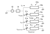
次に、高周波アンテナ13のインピーダンス制御について説明する。図3は、高周波アンテナ13の給電回路を示す図である。この図に示すように、高周波電源15からの高周波電力は整合器14を経て外側アンテナ回路61a、内側アンテナ回路61b、および中間アンテナ回路61cに供給される。ここで、外側アンテナ回路61aは、外側アンテナ部13aと可変コンデンサ21aで構成され、中間アンテナ回路61cは中間アンテナ回路13cと可変コンデンサ21cで構成されているから、外側アンテナ回路61aのインピーダンスZoutは可変コンデンサ21aのポジションを調節してその容量を変化させることにより変化させることができ、中間アンテナ回路61cのインピーダンスZmiddleは可変コンデンサ21cのポジションを調節してその容量を変化させることにより変化させることができる。一方、内側アンテナ回路61bは内側アンテナ部13bのみからなり、そのインピーダンスZinは固定である。このとき、外側アンテナ回路61aの電流IoutはインピーダンスZoutの変化に対応して変化させることができ、中間アンテナ回路61cの電流ImiddleはインピーダンスZmiddleの変化に対応して変化させることができる。そして、内側アンテナ回路61bの電流IinはZoutとZmiddleとZinの比率に応じて変化する。したがって、可変コンデンサ21a,21cの容量調節によってZoutおよびZmiddleを変化させることにより、外側アンテナ回路61aの電流Ioutと内側アンテナ回路61bの電流Iinと中間アンテナ回路61cの電流Imiddleを自在に変化させることができる。そして、このように外側アンテナ部13aに流れる電流と内側アンテナ部13bに流れる電流と中間アンテナ部13cに流れる電流を制御することによってプラズマ密度分布を制御することができる。
Next, impedance control of the
次に、以上のように構成される誘導結合プラズマ処理装置を用いてLCDガラス基板Gに対してプラズマアッシング処理を施す際の処理動作について説明する。 Next, a processing operation when performing a plasma ashing process on the LCD glass substrate G using the inductively coupled plasma processing apparatus configured as described above will be described.
まず、ゲートバルブ27を開にした状態でそこから搬送機構(図示せず)により基板Gを処理室4内に搬入し、載置台23の載置面に載置した後、静電チャック(図示せず)により基板Gを載置台23上に固定する。次に、処理室4内に処理ガス供給系20から処理ガスをシャワー筐体11のガス吐出孔12aから処理室4内に吐出させるとともに、排気装置30により排気管31を介して処理室4内を真空排気することにより、処理室内を例えば0.66〜26.6Pa程度の圧力雰囲気に維持する。
First, after the
また、このとき基板Gの裏面側の冷却空間には、基板Gの温度上昇や温度変化を回避するために、Heガス流路41を介して、熱伝達用ガスとしてHeガスを供給する。
At this time, He gas is supplied to the cooling space on the back side of the substrate G as a heat transfer gas via the He
次いで、高周波電源15から例えば13.56MHzの高周波を高周波アンテナ13に印加し、これにより誘電体壁2を介して処理室4内に誘導電界を形成する。このようにして形成された誘導電界により、処理室4内で処理ガスがプラズマ化し、高密度の誘導結合プラズマが生成され、このプラズマにより例えばプラズマアッシング処理が進行する。
Next, a high frequency of, for example, 13.56 MHz is applied from the high
この場合に、高周波アンテナ13は、上述のように、外側部分においてアンテナ線を密に配置してなる外側アンテナ部13aと、内側部分においてアンテナ線を密に配置してなる内側アンテナ部13bと、これらの間に密に配置してなる中間アンテナ部13cとを有する構造であるので、ガラス基板Gのサイズが1辺1mを超える大型のものの場合であっても、各アンテナ部の間でのプラズマ密度の低下によるプラズマの不均一が生じ難くなる。すなわち、上記特許文献1に記載されているような外側アンテナ部と内側アンテナ部のみで高周波アンテナ13を構成する場合、1辺1mを超えるガラス基板Gに対応するように、高周波アンテナ13をそのまま拡大すると、プラズマ密度を保つ要請から誘電体壁2と載置台23のギャップは変化させないため、外側アンテナ部と内側アンテナ部との間隔が広がった分、プラズマの拡散による均一化効果が低下し、アンテナパターンの密・疎の分布が反映されやすくなってプラズマ密度の分布が悪化するが、本実施形態のように、外側アンテナ部13aと内側アンテナ部13bとの間に中間アンテナ部13cを設けることにより、このようなことを回避することができる。
In this case, as described above, the high-
また、外側アンテナ部13a、内側アンテナ部13b、中間アンテナ部13cは、アンテナ線を均一に配置した場合には、これら配置領域において電界強度が不均一になり、また、各アンテナ部の配置領域間で電界強度が不均一になるが、本実施形態では、これらによる電界強度の不均一が極力生じないような配置形態を採用しているので、電界強度の不均一にともなうプラズマの不均一が生じ難い。
Further, when the antenna lines are arranged uniformly in the
具体的には、矩形状の外側アンテナ部13a、内側アンテナ部13b、中間アンテナ部13cは、その各辺の中央部において電界強度が高くなる傾向があるが、その部分において他の部分よりも巻き数が少なくなっているので、各アンテナ部の配置領域において、電界強度を均一にすることができる。また、渦巻き状のアンテナを構成する場合には、外側に行くに従ってアンテナ線の長さが長くなり電界強度が大きくなるが、内側から外側に向かって巻き数が少なくなるように、より具体的には、各辺の中央部において、内側アンテナ部13bが4巻き、中間アンテナ部13cが3巻き、外側アンテナ部13aが2巻きとなるように、外側アンテナ部13a、内側アンテナ部13b、中間アンテナ部13cが配置されているので、各アンテナ部の配置領域間での電界強度の均一化が可能となる。
Specifically, the rectangular
また、高周波アンテナ13は、外側アンテナ部13aに可変コンデンサ21aを接続して、外側アンテナ回路61aのインピーダンス調整を可能にし、中間アンテナ部13に可変コンデンサ21cを接続して、中間アンテナ回路61cのインピーダンス調節を可能にしたので、外側アンテナ回路61aの電流Ioutと内側アンテナ回路61bの電流Iinと中間アンテナ回路61cの電流Imiddleを自在に変化させることができる。すなわち、可変コンデンサ21a、21cのポジションを調節することにより、外側アンテナ部13aに流れる電流と、内側アンテナ部13bに流れる電流と、中間アンテナ部13cに流れる電流とを制御することができる。誘導結合プラズマは、高周波アンテナ13直下の空間でプラズマを生成させるが、その際の各位置でのプラズマ密度は、各位置での電界強度に比例するため、このように外側アンテナ部13aに流れる電流と内側アンテナ部13bに流れる電流と中間アンテナ部13cに流れる電流を制御することにより、プラズマ密度分布を制御することが可能となる。
Further, the
この場合に、アプリケーションごとに最適なプラズマ密度分布を把握し、予めそのプラズマ密度分布が得られる可変コンデンサ21a,21cのポジションを記憶部52に設定しておくことにより、制御部50によりアプリケーションごとに最適な可変コンデンサ21a,21cのポジションを選択してプラズマ処理を行えるようにすることができる。
In this case, the optimum plasma density distribution for each application is grasped, and the positions of the
このようにして可変コンデンサ21a,21cによるインピーダンス制御によりプラズマ密度分布を制御することができるので、アンテナを交換する必要がなく、アンテナ交換の労力やアプリケーションごとにアンテナを準備しておくコストが不要となる。また、可変コンデンサ21のポジション調節によりきめ細かな電流制御を行うことができ、アプリケーションに応じて最適なプラズマ密度分布が得られるように制御することが可能となる。
Since the plasma density distribution can be controlled by the impedance control by the
なお、本発明は上記実施形態に限定されることなく種々変形可能である。例えば、上記実施形態では、3つのアンテナ部を設けた場合について示したが、これに限らず基板の大きさに対応して4つ以上のアンテナ部を設けてもよい。4つのアンテナ部を設ける場合には、例えば図4に示すように構成することができる。すなわち、図2の外側アンテナ部13aのさらに外側に、最外側アンテナ部13dを設けた構成とすることができる。この例では、最外側アンテナ部13dは、4つのアンテナ線を90°ずつ位置をずらして全体が略矩形状になるように、かつ辺の中央部が1重となるように配置されている。そして最外側アンテナ部13dの各アンテナ線へは4つの端子22dを介して給電されるようになっており、それらの外端部はコンデンサ18dを介して接地されている。ただし、コンデンサ18dは必須ではない。この場合の高周波アンテナ13の給電回路は、図5に示すように、図3の給電回路に最外側アンテナ部13dと可変コンデンサ21dで構成された最外側アンテナ回路61dが付加されたものとなる。最外側アンテナ回路61dのインピーダンスZoutermostは可変コンデンサ21dのポジションを調節してその容量を変化させることにより変化させることができ、最外側アンテナ回路61dの電流IoutermostはインピーダンスZoutermostの変化に対応して変化させることができる。
The present invention can be variously modified without being limited to the above embodiment. For example, in the above embodiment, the case where three antenna units are provided has been described. However, the present invention is not limited to this, and four or more antenna units may be provided corresponding to the size of the substrate. In the case of providing four antenna portions, for example, the configuration can be configured as shown in FIG. That is, the
また、上記実施形態では、内側アンテナ部13bの辺の中央部において4巻き、中間アンテナ部13cの辺の中央部において3巻き、外側アンテナ部13aの辺の中央部において2巻きになるようにした例を示したが、このような構成に限るものではない。
Moreover, in the said embodiment, it was made 4 turns in the center part of the side of the inner
さらに、上記実施形態では、可変コンデンサを外側アンテナ部13aと中間アンテナ部13cに接続した例を示したが、これに限らず、外側アンテナ部13a、中間アンテナ部13c、内側アンテナ部13bのいずれか2つに設ければ同様の機能を得ることができるし、調整したい領域が限られている場合には、いずれか1つに設けるようにしてもよい。
Furthermore, in the above-described embodiment, an example in which a variable capacitor is connected to the
さらにまた、上記実施形態ではインピーダンスを調整するために可変コンデンサを設けたが、可変コイル等他のインピーダンス調整手段であってもよい。 Furthermore, in the above embodiment, the variable capacitor is provided to adjust the impedance, but other impedance adjusting means such as a variable coil may be used.
さらにまた、本発明をアッシング装置に適用した場合について示したが、アッシング装置に限らず、エッチングや、CVD成膜等の他のプラズマ処理装置に適用することができる。さらにまた、被処理体としてFPD基板を用いたが、本発明はこれに限らず半導体ウエハ等他の基板を処理する場合にも適用可能である。 Furthermore, although the case where the present invention is applied to an ashing apparatus is shown, the present invention can be applied not only to the ashing apparatus but also to other plasma processing apparatuses such as etching and CVD film formation. Furthermore, although the FPD substrate is used as the object to be processed, the present invention is not limited to this and is applicable to the case of processing other substrates such as a semiconductor wafer.
1;本体容器
2;誘電体壁(誘電体部材)
3;アンテナ室
4;処理室
13;高周波アンテナ
13a;外側アンテナ部
13b;内側アンテナ部
13c;中間アンテナ部
14;整合器
15;高周波電源
16a,16b,16c;給電部材
20;処理ガス供給系
21a,21c;可変ンサコンデンサ
23;載置台
30;排気装置
50;制御部
51;ユーザーインターフェース
52;記憶部
61a;外側アンテナ回路
61b;内側アンテナ回路
61c;中間アンテナ回路
G;基板
1;
3; Antenna chamber 4; Processing
Claims (4)
前記処理室内で被処理体が載置される載置台と、
前記処理室内に処理ガスを供給する処理ガス供給系と、
前記処理室内を排気する排気系と、
前記処理室の外部に誘電体部材を介して配置され、高周波電力が供給されることにより前記処理室内に誘導電界を形成する同心状に設けられた3以上のアンテナ部を有する高周波アンテナと、
前記各アンテナ部を含むアンテナ回路のうち少なくとも一つのインピーダンスを調節し、これにより前記アンテナ部の電流値を制御するインピーダンス調節手段と
を具備し、
前記各アンテナ部は、該アンテナ部自体が略矩形状になるように複数のアンテナ線が渦巻き状に配置されてなる多重アンテナを構成し、かつその配置領域において均一な電界が形成されるようにその巻き方が設定され、
各アンテナ部の配置領域間で電界の均一化が可能なように、内側のアンテナ部から外側のアンテナ部に向かって、前記各アンテナ部の各辺の中央部において巻き数が少なくなるように各アンテナ線の巻き数が設定されることを特徴とする誘導結合プラズマ処理装置。 A processing chamber for accommodating a rectangular object to be processed and performing plasma processing;
A mounting table on which the object to be processed is mounted in the processing chamber;
A processing gas supply system for supplying a processing gas into the processing chamber;
An exhaust system for exhausting the processing chamber;
A high-frequency antenna having three or more antenna portions disposed concentrically to form an induction electric field in the processing chamber by being provided with a dielectric member outside the processing chamber and supplied with high-frequency power;
Adjusting an impedance of at least one of the antenna circuits including the antenna parts, thereby providing an impedance adjusting means for controlling a current value of the antenna part;
Each antenna unit constitutes a multiple antenna in which a plurality of antenna wires are spirally arranged so that the antenna unit itself is substantially rectangular, and a uniform electric field is formed in the arrangement region. The winding method is set,
The number of turns is reduced at the center of each side of each antenna part from the inner antenna part to the outer antenna part so that the electric field can be made uniform between the arrangement areas of each antenna part. An inductively coupled plasma processing apparatus, wherein the number of turns of an antenna wire is set.
Priority Applications (1)
| Application Number | Priority Date | Filing Date | Title |
|---|---|---|---|
| JP2013146049A JP5674871B2 (en) | 2013-07-12 | 2013-07-12 | Inductively coupled plasma processing equipment |
Applications Claiming Priority (1)
| Application Number | Priority Date | Filing Date | Title |
|---|---|---|---|
| JP2013146049A JP5674871B2 (en) | 2013-07-12 | 2013-07-12 | Inductively coupled plasma processing equipment |
Related Parent Applications (1)
| Application Number | Title | Priority Date | Filing Date |
|---|---|---|---|
| JP2008127166A Division JP5551343B2 (en) | 2008-05-14 | 2008-05-14 | Inductively coupled plasma processing equipment |
Publications (2)
| Publication Number | Publication Date |
|---|---|
| JP2013258409A JP2013258409A (en) | 2013-12-26 |
| JP5674871B2 true JP5674871B2 (en) | 2015-02-25 |
Family
ID=49954544
Family Applications (1)
| Application Number | Title | Priority Date | Filing Date |
|---|---|---|---|
| JP2013146049A Active JP5674871B2 (en) | 2013-07-12 | 2013-07-12 | Inductively coupled plasma processing equipment |
Country Status (1)
| Country | Link |
|---|---|
| JP (1) | JP5674871B2 (en) |
Families Citing this family (3)
| Publication number | Priority date | Publication date | Assignee | Title |
|---|---|---|---|---|
| JP6349796B2 (en) * | 2014-03-11 | 2018-07-04 | 東京エレクトロン株式会社 | Plasma processing apparatus, thin film transistor manufacturing method, and storage medium |
| US10971333B2 (en) | 2016-10-24 | 2021-04-06 | Samsung Electronics Co., Ltd. | Antennas, circuits for generating plasma, plasma processing apparatus, and methods of manufacturing semiconductor devices using the same |
| JP7352068B2 (en) * | 2019-07-12 | 2023-09-28 | 日新電機株式会社 | plasma control system |
Family Cites Families (4)
| Publication number | Priority date | Publication date | Assignee | Title |
|---|---|---|---|---|
| JP3462865B2 (en) * | 2001-07-10 | 2003-11-05 | 三菱重工業株式会社 | Feeding antenna and semiconductor manufacturing apparatus |
| US7571697B2 (en) * | 2001-09-14 | 2009-08-11 | Lam Research Corporation | Plasma processor coil |
| JP2004356511A (en) * | 2003-05-30 | 2004-12-16 | Tokyo Electron Ltd | Plasma treatment device |
| JP2007311182A (en) * | 2006-05-18 | 2007-11-29 | Tokyo Electron Ltd | Inductively-coupled plasma processing device, and plasma processing method |
-
2013
- 2013-07-12 JP JP2013146049A patent/JP5674871B2/en active Active
Also Published As
| Publication number | Publication date |
|---|---|
| JP2013258409A (en) | 2013-12-26 |
Similar Documents
| Publication | Publication Date | Title |
|---|---|---|
| JP5551343B2 (en) | Inductively coupled plasma processing equipment | |
| JP5566498B2 (en) | Inductively coupled plasma processing apparatus, plasma processing method, and storage medium | |
| KR101956478B1 (en) | Antenna unit for inductively coupled plasma, inductively coupled plasma processing apparatus and method therefor | |
| TWI445460B (en) | Induction coupling plasma processing device and plasma processing method | |
| JP5666991B2 (en) | Inductively coupled plasma antenna unit and inductively coupled plasma processing apparatus | |
| JP5329167B2 (en) | Inductively coupled plasma processing apparatus, inductively coupled plasma processing method, and storage medium | |
| JP3880864B2 (en) | Inductively coupled plasma processing equipment | |
| JP5597071B2 (en) | Antenna unit and inductively coupled plasma processing apparatus | |
| JP2016225018A (en) | Gas processing device and multi-division shower head used for the same | |
| JP2013077715A (en) | Antenna unit for inductive coupling plasma, and inductive coupling plasma processing device | |
| JP5894785B2 (en) | Inductively coupled plasma antenna unit and inductively coupled plasma processing apparatus | |
| KR101754439B1 (en) | Inductively coupled plasma processing method and inductively coupled plasma processing apparatus | |
| JP5674871B2 (en) | Inductively coupled plasma processing equipment | |
| JP2006344998A (en) | Inductive coupling plasma treatment apparatus | |
| JP6261220B2 (en) | Inductively coupled plasma processing equipment | |
| JP2014154684A (en) | Inductively coupled plasma processing apparatus | |
| TWI600048B (en) | Inductively coupled plasma processing device |
Legal Events
| Date | Code | Title | Description |
|---|---|---|---|
| A977 | Report on retrieval |
Free format text: JAPANESE INTERMEDIATE CODE: A971007 Effective date: 20140530 |
|
| A131 | Notification of reasons for refusal |
Free format text: JAPANESE INTERMEDIATE CODE: A131 Effective date: 20140610 |
|
| A521 | Request for written amendment filed |
Free format text: JAPANESE INTERMEDIATE CODE: A523 Effective date: 20140729 |
|
| TRDD | Decision of grant or rejection written | ||
| A01 | Written decision to grant a patent or to grant a registration (utility model) |
Free format text: JAPANESE INTERMEDIATE CODE: A01 Effective date: 20141209 |
|
| A61 | First payment of annual fees (during grant procedure) |
Free format text: JAPANESE INTERMEDIATE CODE: A61 Effective date: 20141222 |
|
| R150 | Certificate of patent or registration of utility model |
Ref document number: 5674871 Country of ref document: JP Free format text: JAPANESE INTERMEDIATE CODE: R150 |
|
| R250 | Receipt of annual fees |
Free format text: JAPANESE INTERMEDIATE CODE: R250 |
|
| R250 | Receipt of annual fees |
Free format text: JAPANESE INTERMEDIATE CODE: R250 |
|
| R250 | Receipt of annual fees |
Free format text: JAPANESE INTERMEDIATE CODE: R250 |
|
| R250 | Receipt of annual fees |
Free format text: JAPANESE INTERMEDIATE CODE: R250 |