JP5662037B2 - 不揮発性メモリに対してデータの読み出しおよび書き込みを行うためのデータホワイトニング - Google Patents
不揮発性メモリに対してデータの読み出しおよび書き込みを行うためのデータホワイトニング Download PDFInfo
- Publication number
- JP5662037B2 JP5662037B2 JP2010046014A JP2010046014A JP5662037B2 JP 5662037 B2 JP5662037 B2 JP 5662037B2 JP 2010046014 A JP2010046014 A JP 2010046014A JP 2010046014 A JP2010046014 A JP 2010046014A JP 5662037 B2 JP5662037 B2 JP 5662037B2
- Authority
- JP
- Japan
- Prior art keywords
- data
- information
- memory
- secret
- volatile memory
- Prior art date
- Legal status (The legal status is an assumption and is not a legal conclusion. Google has not performed a legal analysis and makes no representation as to the accuracy of the status listed.)
- Expired - Fee Related
Links
Images


Classifications
-
- G—PHYSICS
- G06—COMPUTING; CALCULATING OR COUNTING
- G06F—ELECTRIC DIGITAL DATA PROCESSING
- G06F12/00—Accessing, addressing or allocating within memory systems or architectures
- G06F12/14—Protection against unauthorised use of memory or access to memory
- G06F12/1408—Protection against unauthorised use of memory or access to memory by using cryptography
-
- G—PHYSICS
- G06—COMPUTING; CALCULATING OR COUNTING
- G06F—ELECTRIC DIGITAL DATA PROCESSING
- G06F21/00—Security arrangements for protecting computers, components thereof, programs or data against unauthorised activity
- G06F21/70—Protecting specific internal or peripheral components, in which the protection of a component leads to protection of the entire computer
- G06F21/71—Protecting specific internal or peripheral components, in which the protection of a component leads to protection of the entire computer to assure secure computing or processing of information
- G06F21/72—Protecting specific internal or peripheral components, in which the protection of a component leads to protection of the entire computer to assure secure computing or processing of information in cryptographic circuits
-
- G—PHYSICS
- G06—COMPUTING; CALCULATING OR COUNTING
- G06F—ELECTRIC DIGITAL DATA PROCESSING
- G06F21/00—Security arrangements for protecting computers, components thereof, programs or data against unauthorised activity
- G06F21/70—Protecting specific internal or peripheral components, in which the protection of a component leads to protection of the entire computer
- G06F21/78—Protecting specific internal or peripheral components, in which the protection of a component leads to protection of the entire computer to assure secure storage of data
- G06F21/79—Protecting specific internal or peripheral components, in which the protection of a component leads to protection of the entire computer to assure secure storage of data in semiconductor storage media, e.g. directly-addressable memories
-
- G—PHYSICS
- G11—INFORMATION STORAGE
- G11C—STATIC STORES
- G11C16/00—Erasable programmable read-only memories
- G11C16/02—Erasable programmable read-only memories electrically programmable
- G11C16/06—Auxiliary circuits, e.g. for writing into memory
- G11C16/10—Programming or data input circuits
-
- G—PHYSICS
- G11—INFORMATION STORAGE
- G11C—STATIC STORES
- G11C16/00—Erasable programmable read-only memories
- G11C16/02—Erasable programmable read-only memories electrically programmable
- G11C16/06—Auxiliary circuits, e.g. for writing into memory
- G11C16/22—Safety or protection circuits preventing unauthorised or accidental access to memory cells
-
- G—PHYSICS
- G06—COMPUTING; CALCULATING OR COUNTING
- G06F—ELECTRIC DIGITAL DATA PROCESSING
- G06F12/00—Accessing, addressing or allocating within memory systems or architectures
- G06F12/02—Addressing or allocation; Relocation
- G06F12/0223—User address space allocation, e.g. contiguous or non contiguous base addressing
- G06F12/023—Free address space management
- G06F12/0238—Memory management in non-volatile memory, e.g. resistive RAM or ferroelectric memory
- G06F12/0246—Memory management in non-volatile memory, e.g. resistive RAM or ferroelectric memory in block erasable memory, e.g. flash memory
-
- G—PHYSICS
- G06—COMPUTING; CALCULATING OR COUNTING
- G06F—ELECTRIC DIGITAL DATA PROCESSING
- G06F2221/00—Indexing scheme relating to security arrangements for protecting computers, components thereof, programs or data against unauthorised activity
- G06F2221/21—Indexing scheme relating to G06F21/00 and subgroups addressing additional information or applications relating to security arrangements for protecting computers, components thereof, programs or data against unauthorised activity
- G06F2221/2107—File encryption
Description
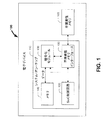
適用例1:システムであって、不揮発性メモリと、システム・オン・チップ(SoC)と、を備え、
前記システム・オン・チップは、非秘密データおよびメモリ管理データの内の少なくとも一方を含むデータをホワイトニングするよう構成された暗号化モジュールと、前記暗号化モジュールに接続され、前記ホワイトニングされたデータを前記不揮発性メモリに格納するよう構成されたメモリインターフェースと、を備える、システム。
適用例2:適用例1に記載のシステムであって、前記暗号化モジュールは、次世代標準暗号化方式(AES)エンジンを備える、システム。
適用例3:適用例1に記載のシステムであって、前記データは、秘密データをさらに含み、前記SoCは、前記秘密データおよび非秘密データを前記不揮発性メモリとやり取りするためのコマンドを前記メモリインターフェースに発行するよう構成されたファイルシステムをさらに含み、前記メモリインターフェースは、前記不揮発性メモリ内の前記秘密データまたは前記非秘密データの格納を管理するための前記メモリ管理データを生成するよう構成されたメモリトランスレーションレイヤを備える、システム。
適用例4:適用例3に記載のシステムであって、前記ファイルシステムは、さらに、前記秘密データと共に暗号鍵を提供し、前記非秘密データと共に暗号鍵を提供しないよう構成されている、システム。
適用例5:不揮発性メモリ内のユーザデータの格納を管理するための装置であって、前記ユーザデータのためのメモリ管理データを生成する手段と、前記メモリ管理データを格納する前記不揮発性メモリの第1の物理アドレスを選択する手段と、前記選択された第1の物理アドレスに基づいて、第1の暗号化シードを算出する手段と、前記選択された第1の物理アドレスに格納するために、前記第1の暗号化シードを用いて前記メモリ管理データを暗号化する手段と、を備える、装置。
適用例6:適用例5に記載の装置であって、さらに、前記不揮発性メモリに前記ランダム化されたメモリ管理データをプログラミングする手段を備える、装置。
適用例7:適用例5に記載の装置であって、前記暗号化する手段は、次世代標準暗号化方式(AES)エンジンを備え、前記第1の暗号化シードは、初期ベクトルを含む、装置。
適用例8:適用例7に記載の装置であって、さらに、前記AESエンジンのための秘密鍵として所定の鍵を選択する手段を備え、前記所定の鍵は、前記選択された第1の物理アドレスの値に依存しない、装置。
適用例9:適用例5に記載の装置であって、前記メモリ管理データは、前記ユーザデータの論理アドレスを前記ユーザデータの物理アドレスと関連づけるメモリマップ情報を含む、装置。
適用例10:適用例5に記載の装置であって、さらに、第1の物理アドレスから第2の物理アドレスに前記メモリ管理データを移動させる手段を備え、前記移動させる手段は、前記第1の暗号化シードを用いて前記メモリ管理データを復号するよう前記暗号化モジュールに指示する手段と、前記第2の物理アドレスに基づいて第2の暗号化シードを算出する手段と、前記不揮発性メモリの前記第2の物理アドレスに格納するために、前記第2の暗号化シードを用いて前記メモリ管理データを暗号化するよう、前記暗号化する手段に指示する手段と、を備える、装置。
適用例11:システムであって、暗号化モジュールと、不揮発性メモリを管理するためのメモリインターフェースであって、前記暗号化モジュールと通信するよう動作可能であるメモリインターフェースと、を備え、
前記インターフェースは、非秘密データを含む情報を論理アドレスに格納するためのコマンドを受信し、前記論理アドレスに基づいて暗号化シードを生成し、前記不揮発性メモリの第1の物理アドレスに格納するために、前記暗号化シードを用いて前記情報を暗号化するよう、前記暗号化モジュールに指示し、前記第1の物理アドレスから前記不揮発性メモリの第2の物理アドレスに前記暗号化された情報を移動させる時に、前記情報の復号を迂回するよう構成されている、システム。
適用例12:適用例1または11に記載のシステムであって、前記不揮発性メモリはNAND型フラッシュメモリを含む、システム。
適用例13:適用例11に記載のシステムであって、前記メモリインターフェースは、さらに、前記コマンドが少なくとも1つの暗号化シードを欠いていることに基づいて、前記情報が非秘密データを含むことを検出するよう構成されている、システム。
適用例14:適用例11に記載のシステムであって、前記メモリインターフェースは、前記不揮発性メモリのガベージコレクションを開始するよう構成されており、前記暗号化された情報は、前記ガベージコレクション中に、前記第1の物理アドレスから前記第2の物理アドレスに移動される、システム。
適用例15:適用例11に記載のシステムであって、前記メモリインターフェースは、ファイルシステムと通信するよう動作可能であり、前記コマンドは、前記ファイルシステムから受信される、システム。
適用例16:適用例11に記載のシステムであって、前記メモリインターフェースは、さらに、前記論理アドレスを前記第2の物理アドレスに関連づけるように、メモリ管理データを更新し、前記論理アドレスから前記情報を取り出すための読み出しコマンドを受信し、前記メモリ管理データを用いて、前記第2の物理ロケーションを決定し、前記論理アドレスに基づいて前記暗号化シードを再生成し、前記再生成された暗号化シードを用いて前記情報を復号するよう、前記暗号化モジュールに指示するように構成されている、システム。
適用例17:メモリインターフェースを用いて不揮発性メモリを管理する方法であって、前記不揮発性メモリに格納する情報を受信する工程と、前記情報が、秘密情報であるか非秘密情報であるかを検出する工程と、前記検出に基づいて、プライベート鍵およびホワイトニング鍵のいずれかを選択する工程と、前記選択された鍵を用いた前記情報の暗号化を有効にして、前記不揮発性メモリに格納する前記情報を暗号化する工程と、を備える、方法。
適用例18:適用例17に記載の方法であって、前記検出する工程は、前記プライベート鍵が、前記不揮発性メモリに前記情報を書き込むためのコマンドと共に受信されたか否かを判定する工程を備える、方法。
適用例19:適用例17に記載の方法であって、前記ホワイトニング鍵の値は、前記情報および前記情報に関連づけられたアドレスに依存しない、方法。
適用例20:適用例17に記載の方法であって、さらに、前記情報が秘密情報であると検出された場合に、第1の初期化ベクトルを受信する工程と、前記情報が非秘密情報であると検出された場合に、第2の初期化ベクトルを生成する工程と、前記情報が秘密情報であるか非秘密情報であるかに基づいて、前記第1および第2の初期化ベクトルのいずれかを選択する工程と、を備える、方法。
適用例21:適用例17に記載の方法であって、さらに、前記受信した情報のメモリ管理データを生成する工程と、前記不揮発性メモリに格納するために、前記ホワイトニング鍵を用いた前記メモリ管理データの暗号化を有効にする工程と、を備える、方法。
適用例22:メモリインターフェースを用いて不揮発性メモリに格納する情報を準備する方法であって、前記情報は論理アドレスに関連づけられており、前記方法は、前記論理アドレスに基づいて前記情報を暗号化する工程と、前記論理アドレスを前記不揮発性メモリの第1の物理アドレスと対応づけるメモリ管理データを生成する工程と、前記不揮発性メモリの第2の物理アドレスに基づいて前記メモリ管理データを暗号化する工程と、前記第1の物理アドレスに前記暗号化された情報を格納する工程と、前記不揮発性メモリの前記第2の物理アドレスに前記暗号化されたメモリ管理データを格納する工程と、を備える、方法。
適用例23:適用例22に記載の方法であって、さらに、前記第1の物理アドレスから前記不揮発性メモリの第3の物理アドレスに前記暗号化された情報を移動させる工程を備え、前記暗号化された情報は、前記移動させる工程の間、暗号化されたままである、方法。
適用例24:適用例17または22に記載の方法であって、前記不揮発性メモリはNAND型フラッシュメモリを含む、方法。
適用例25:適用例22に記載の方法であって、前記不揮発性メモリは、複数のページを有するNAN型フラッシュメモリを含み、前記第1および第2の物理アドレスの各々は、前記複数のページの内の1つに関連づけられる、方法。
Claims (9)
- 不揮発性メモリを管理するためのシステムであって、
不揮発性メモリと、
システム・オン・チップ(SoC)と、
を備え、
前記システム・オン・チップは、
データをホワイトニングするよう構成された暗号化モジュールと、
前記暗号化モジュールに接続され、受け取ったデータが非秘密データまたは秘密データのいずれであるかを検出するように構成されたメモリインターフェースと、を備え、
前記受け取ったデータが非秘密データである場合、前記暗号化モジュールは前記受け取った非秘密データをホワイトニングし、前記メモリインターフェースは前記ホワイトニングされた非秘密データを前記不揮発性メモリ内に格納する、システム。 - 請求項1に記載のシステムであって、前記暗号化モジュールは、次世代標準暗号化方式(AES)エンジンを備える、システム。
- 請求項1に記載のシステムであって、
前記SoCは、前記秘密データおよび非秘密データを前記不揮発性メモリとやり取りするためのコマンドを前記メモリインターフェースに発行するよう構成されたファイルシステムをさらに含み、
前記メモリインターフェースは、前記不揮発性メモリ内の前記秘密データまたは前記非秘密データの格納を管理するためのメモリ管理データを生成するよう構成されたメモリトランスレーションレイヤを備える、システム。 - 請求項3に記載のシステムであって、前記ファイルシステムは、さらに、
前記秘密データと共に暗号鍵を提供し、前記非秘密データと共に暗号鍵を提供しないよう構成されている、システム。 - メモリインターフェースを用いて不揮発性メモリを管理する方法であって、
前記不揮発性メモリに格納する情報を受信する工程と、
前記情報が、秘密情報であるか非秘密情報であるかを検出する工程と、
前記検出に基づいて、プライベート鍵およびホワイトニング鍵のいずれかを選択する工程と、前記ホワイトニング鍵は前記情報が非秘密情報である場合に選択され、
前記情報が非秘密情報である場合に、前記選択されたホワイトニング鍵を用いた前記情報のホワイトニングを有効にして、前記不揮発性メモリに格納する前記情報をホワイトニングする工程と、
を備える、方法。 - 請求項5に記載の方法であって、前記検出する工程は、前記プライベート鍵が、前記不揮発性メモリに前記情報を書き込むためのコマンドと共に受信されたか否かを判定する工程を備える、方法。
- 請求項5に記載の方法であって、前記ホワイトニング鍵の値は、前記情報および前記情報に関連づけられたアドレスに依存しない、方法。
- 請求項5に記載の方法であって、さらに、
前記情報が秘密情報であると検出された場合に、第1の初期化ベクトルを受信する工程と、
前記情報が非秘密情報であると検出された場合に、第2の初期化ベクトルを生成する工程と、
前記情報が秘密情報であるか非秘密情報であるかに基づいて、前記第1および第2の初期化ベクトルのいずれかを選択する工程と、
を備える、方法。 - 請求項5に記載の方法であって、さらに、
前記受信した情報のメモリ管理データを生成する工程と、
前記不揮発性メモリに格納するために、前記ホワイトニング鍵を用いた前記メモリ管理データの暗号化を有効にする工程と、
を備える、方法。
Applications Claiming Priority (2)
| Application Number | Priority Date | Filing Date | Title |
|---|---|---|---|
| US12/398,090 | 2009-03-04 | ||
| US12/398,090 US8589700B2 (en) | 2009-03-04 | 2009-03-04 | Data whitening for writing and reading data to and from a non-volatile memory |
Publications (3)
| Publication Number | Publication Date |
|---|---|
| JP2010231778A JP2010231778A (ja) | 2010-10-14 |
| JP2010231778A5 JP2010231778A5 (ja) | 2013-03-21 |
| JP5662037B2 true JP5662037B2 (ja) | 2015-01-28 |
Family
ID=42097383
Family Applications (1)
| Application Number | Title | Priority Date | Filing Date |
|---|---|---|---|
| JP2010046014A Expired - Fee Related JP5662037B2 (ja) | 2009-03-04 | 2010-03-03 | 不揮発性メモリに対してデータの読み出しおよび書き込みを行うためのデータホワイトニング |
Country Status (5)
| Country | Link |
|---|---|
| US (2) | US8589700B2 (ja) |
| EP (1) | EP2226810A1 (ja) |
| JP (1) | JP5662037B2 (ja) |
| KR (2) | KR101155697B1 (ja) |
| WO (1) | WO2010101598A1 (ja) |
Families Citing this family (47)
| Publication number | Priority date | Publication date | Assignee | Title |
|---|---|---|---|---|
| US8832458B2 (en) * | 2005-03-22 | 2014-09-09 | Seagate Technology Llc | Data transcription in a data storage device |
| WO2008070814A2 (en) | 2006-12-06 | 2008-06-12 | Fusion Multisystems, Inc. (Dba Fusion-Io) | Apparatus, system, and method for a scalable, composite, reconfigurable backplane |
| US8589700B2 (en) * | 2009-03-04 | 2013-11-19 | Apple Inc. | Data whitening for writing and reading data to and from a non-volatile memory |
| JP5492679B2 (ja) * | 2009-06-30 | 2014-05-14 | パナソニック株式会社 | 記憶装置およびメモリコントローラ |
| US8250380B2 (en) * | 2009-12-17 | 2012-08-21 | Hitachi Global Storage Technologies Netherlands B.V. | Implementing secure erase for solid state drives |
| KR20120002760A (ko) * | 2010-07-01 | 2012-01-09 | 삼성전자주식회사 | 낸드 플래쉬 메모리의 동작 신뢰성을 향상시키는 데이터 기록 방법 및 데이터 기록 장치 |
| US20120117303A1 (en) | 2010-11-04 | 2012-05-10 | Numonyx B.V. | Metadata storage associated with flash translation layer |
| JP5664347B2 (ja) * | 2011-03-04 | 2015-02-04 | ソニー株式会社 | 仮想メモリシステム、仮想メモリの制御方法、およびプログラム |
| US8862902B2 (en) * | 2011-04-29 | 2014-10-14 | Seagate Technology Llc | Cascaded data encryption dependent on attributes of physical memory |
| US8705291B2 (en) | 2011-05-27 | 2014-04-22 | Seagate Technology Llc | Sanitizing a non-volatile memory through charge accumulation |
| GB2494625A (en) * | 2011-09-06 | 2013-03-20 | St Microelectronics Grenoble 2 | Minimizing the latency of a scrambled memory access by sending a memory access operation to the encryption engine and the memory controller in parallel |
| US8886963B2 (en) | 2011-09-15 | 2014-11-11 | Apple Inc. | Secure relocation of encrypted files |
| US8751819B1 (en) * | 2011-09-22 | 2014-06-10 | Symantec Corporation | Systems and methods for encoding data |
| KR101871509B1 (ko) * | 2011-12-15 | 2018-06-27 | 주식회사 케이티 | 장치, 게이트웨이, 장치 및 게이트웨이의 데이터 전송 방법, 및 네트워크 어플리케이션 서버 |
| US9117508B2 (en) * | 2012-01-19 | 2015-08-25 | Rambus Inc. | Integrated circuit with adaptive power state management |
| JP5875441B2 (ja) | 2012-03-29 | 2016-03-02 | インターナショナル・ビジネス・マシーンズ・コーポレーションInternational Business Machines Corporation | データを暗号化する装置及び方法 |
| KR101975027B1 (ko) * | 2012-05-04 | 2019-05-03 | 삼성전자주식회사 | 시스템 온 칩, 이의 동작 방법, 이를 포함하는 장치들 |
| DE102012209404A1 (de) * | 2012-06-04 | 2013-12-05 | Robert Bosch Gmbh | Vorrichtung zur Ausführung eines kryptographischen Verfahrens und Betriebsverfahren hierfür |
| US8924832B1 (en) * | 2012-06-26 | 2014-12-30 | Western Digital Technologies, Inc. | Efficient error handling mechanisms in data storage systems |
| US9881161B2 (en) | 2012-12-06 | 2018-01-30 | S-Printing Solution Co., Ltd. | System on chip to perform a secure boot, an image forming apparatus using the same, and method thereof |
| KR20140073384A (ko) * | 2012-12-06 | 2014-06-16 | 삼성전자주식회사 | 보안 부팅을 수행하는 칩 시스템과 이를 이용하는 화상형성장치 및 그 보안 부팅 방법 |
| US9330275B1 (en) * | 2013-03-28 | 2016-05-03 | Amazon Technologies, Inc. | Location based decryption |
| US9665501B1 (en) | 2013-06-18 | 2017-05-30 | Western Digital Technologies, Inc. | Self-encrypting data storage device supporting object-level encryption |
| US9294266B2 (en) | 2013-06-27 | 2016-03-22 | Qualcomm Incorporated | Method and apparatus to encrypt plaintext data |
| US20160335201A1 (en) * | 2014-01-28 | 2016-11-17 | Hewlett Packard Enterprise Development Lp | Data and instruction set encryption |
| KR20150111692A (ko) * | 2014-03-26 | 2015-10-06 | 삼성전자주식회사 | 메모리 컨트롤러 구동방법 및 메모리 컨트롤러를 포함하는 메모리 시스템 |
| US9830087B2 (en) * | 2014-11-13 | 2017-11-28 | Micron Technology, Inc. | Memory wear leveling |
| CN104598357B (zh) * | 2015-02-12 | 2018-05-08 | 兆讯恒达微电子技术(北京)有限公司 | 一种数据抗干扰保护方法 |
| US9620242B1 (en) | 2015-07-10 | 2017-04-11 | The United States Of America As Represented By The Secretary Of The Navy | Methods and apparatuses including one or more interrupted integrated circuit operations for characterizing radiation effects in integrated circuits |
| US9860841B2 (en) * | 2015-08-20 | 2018-01-02 | Apple Inc. | Communications fabric with split paths for control and data packets |
| US10671762B2 (en) * | 2015-09-29 | 2020-06-02 | Apple Inc. | Unified addressable memory |
| CN105243344B (zh) * | 2015-11-02 | 2020-09-01 | 上海兆芯集成电路有限公司 | 具有硬盘加密功能的芯片组以及主机控制器 |
| US9946744B2 (en) * | 2016-01-06 | 2018-04-17 | General Motors Llc | Customer vehicle data security method |
| US10089025B1 (en) | 2016-06-29 | 2018-10-02 | EMC IP Holding Company LLC | Bloom filters in a flash memory |
| US10055351B1 (en) | 2016-06-29 | 2018-08-21 | EMC IP Holding Company LLC | Low-overhead index for a flash cache |
| US10261704B1 (en) | 2016-06-29 | 2019-04-16 | EMC IP Holding Company LLC | Linked lists in flash memory |
| US10146438B1 (en) | 2016-06-29 | 2018-12-04 | EMC IP Holding Company LLC | Additive library for data structures in a flash memory |
| US10037164B1 (en) * | 2016-06-29 | 2018-07-31 | EMC IP Holding Company LLC | Flash interface for processing datasets |
| US10331561B1 (en) | 2016-06-29 | 2019-06-25 | Emc Corporation | Systems and methods for rebuilding a cache index |
| KR102543267B1 (ko) * | 2016-07-13 | 2023-06-13 | 삼성에스디에스 주식회사 | 화이트박스 암호를 이용한 암/복호화 방법 및 그 장치 |
| US11030102B2 (en) | 2018-09-07 | 2021-06-08 | Apple Inc. | Reducing memory cache control command hops on a fabric |
| US11100011B2 (en) | 2018-12-13 | 2021-08-24 | Sony Semiconductor Israel Ltd. | Flash translation layer with hierarchical security |
| CN112115076A (zh) * | 2019-06-20 | 2020-12-22 | 慧荣科技股份有限公司 | 使用者数据的加解密装置及方法 |
| CN112231719A (zh) * | 2019-07-15 | 2021-01-15 | 美光科技公司 | 密码密钥管理 |
| US11681635B2 (en) | 2020-09-07 | 2023-06-20 | Mellanox Technologies, Ltd. | Secure flash controller |
| US11580091B2 (en) | 2020-11-10 | 2023-02-14 | Northrop Grumman Systems Corporation | Method of ensuring confidentiality and integrity of stored data and metadata in an untrusted environment |
| KR102462829B1 (ko) * | 2021-01-20 | 2022-11-04 | 고려대학교 산학협력단 | Nand 플래시 메모리의 보안 카피-백 프로그램 방법 |
Family Cites Families (31)
| Publication number | Priority date | Publication date | Assignee | Title |
|---|---|---|---|---|
| US5404485A (en) * | 1993-03-08 | 1995-04-04 | M-Systems Flash Disk Pioneers Ltd. | Flash file system |
| US6249866B1 (en) * | 1997-09-16 | 2001-06-19 | Microsoft Corporation | Encrypting file system and method |
| US6785810B1 (en) * | 1999-08-31 | 2004-08-31 | Espoc, Inc. | System and method for providing secure transmission, search, and storage of data |
| US7349987B2 (en) * | 2000-11-13 | 2008-03-25 | Digital Doors, Inc. | Data security system and method with parsing and dispersion techniques |
| US6684289B1 (en) * | 2000-11-22 | 2004-01-27 | Sandisk Corporation | Techniques for operating non-volatile memory systems with data sectors having different sizes than the sizes of the pages and/or blocks of the memory |
| JP4045777B2 (ja) * | 2001-10-30 | 2008-02-13 | 株式会社日立製作所 | 情報処理装置 |
| JP2003242030A (ja) * | 2001-12-14 | 2003-08-29 | Matsushita Electric Ind Co Ltd | メモリ管理装置及びメモリ管理方法 |
| US6715085B2 (en) * | 2002-04-18 | 2004-03-30 | International Business Machines Corporation | Initializing, maintaining, updating and recovering secure operation within an integrated system employing a data access control function |
| US20050050342A1 (en) * | 2003-08-13 | 2005-03-03 | International Business Machines Corporation | Secure storage utility |
| US7152138B2 (en) * | 2004-01-30 | 2006-12-19 | Hewlett-Packard Development Company, L.P. | System on a chip having a non-volatile imperfect memory |
| DE602005015178D1 (de) * | 2004-02-05 | 2009-08-13 | Research In Motion Ltd | Speicherung auf einem chip,erzeugung und handhabung eines geheimschlüssels |
| US7360057B2 (en) * | 2005-03-22 | 2008-04-15 | Seagate Technology, Llc | Encryption of data in a range of logical block addresses |
| US20060224902A1 (en) * | 2005-03-30 | 2006-10-05 | Bolt Thomas B | Data management system for removable storage media |
| US7657754B2 (en) * | 2005-12-08 | 2010-02-02 | Agere Systems Inc | Methods and apparatus for the secure handling of data in a microcontroller |
| US8464073B2 (en) * | 2006-09-13 | 2013-06-11 | Stec, Inc. | Method and system for secure data storage |
| JP2008090451A (ja) * | 2006-09-29 | 2008-04-17 | Toshiba Corp | 記憶装置 |
| US20080107275A1 (en) * | 2006-11-08 | 2008-05-08 | Mehdi Asnaashari | Method and system for encryption of information stored in an external nonvolatile memory |
| US7876894B2 (en) * | 2006-11-14 | 2011-01-25 | Mcm Portfolio Llc | Method and system to provide security implementation for storage devices |
| KR101449673B1 (ko) | 2006-12-24 | 2014-10-13 | 샌디스크 아이엘 엘티디 | 에러 억제를 위해 랜더마이징하는 플래시 메모리 디바이스, 시스템 및 방법 |
| US8127200B2 (en) * | 2006-12-24 | 2012-02-28 | Sandisk Il Ltd. | Flash memory device and system with randomizing for suppressing errors |
| US7984360B2 (en) * | 2006-12-31 | 2011-07-19 | Ramot At Tel Aviv University Ltd. | Avoiding errors in a flash memory by using substitution transformations |
| US8683228B2 (en) * | 2007-01-16 | 2014-03-25 | Terry Lee Stokes | System and method for WORM data storage |
| JP4498370B2 (ja) * | 2007-02-14 | 2010-07-07 | 株式会社東芝 | データ書き込み方法 |
| JP5028577B2 (ja) * | 2007-02-19 | 2012-09-19 | 株式会社メガチップス | メモリ制御方法およびメモリシステム |
| JP2009157836A (ja) * | 2007-12-27 | 2009-07-16 | Toshiba Corp | メモリシステム |
| JP5019611B2 (ja) * | 2007-12-27 | 2012-09-05 | 株式会社東芝 | メモリシステム |
| US8301912B2 (en) * | 2007-12-31 | 2012-10-30 | Sandisk Technologies Inc. | System, method and memory device providing data scrambling compatible with on-chip copy operation |
| US8230158B2 (en) * | 2008-08-12 | 2012-07-24 | Micron Technology, Inc. | Memory devices and methods of storing data on a memory device |
| JP2010108029A (ja) * | 2008-10-28 | 2010-05-13 | Panasonic Corp | 不揮発性メモリコントローラ、不揮発性記憶装置、及び不揮発性記憶システム |
| US9336160B2 (en) * | 2008-10-30 | 2016-05-10 | Qualcomm Incorporated | Low latency block cipher |
| US8589700B2 (en) * | 2009-03-04 | 2013-11-19 | Apple Inc. | Data whitening for writing and reading data to and from a non-volatile memory |
-
2009
- 2009-03-04 US US12/398,090 patent/US8589700B2/en active Active
- 2009-12-21 WO PCT/US2009/069050 patent/WO2010101598A1/en active Application Filing
-
2010
- 2010-02-22 EP EP10154213A patent/EP2226810A1/en not_active Withdrawn
- 2010-03-03 JP JP2010046014A patent/JP5662037B2/ja not_active Expired - Fee Related
- 2010-03-03 KR KR1020100019023A patent/KR101155697B1/ko active IP Right Grant
-
2011
- 2011-10-26 KR KR1020110109798A patent/KR101534370B1/ko active IP Right Grant
-
2013
- 2013-11-18 US US14/082,940 patent/US8918655B2/en active Active
Also Published As
| Publication number | Publication date |
|---|---|
| US8589700B2 (en) | 2013-11-19 |
| US20140075208A1 (en) | 2014-03-13 |
| KR101155697B1 (ko) | 2012-06-12 |
| US20100229005A1 (en) | 2010-09-09 |
| KR20110134339A (ko) | 2011-12-14 |
| WO2010101598A1 (en) | 2010-09-10 |
| EP2226810A1 (en) | 2010-09-08 |
| JP2010231778A (ja) | 2010-10-14 |
| KR101534370B1 (ko) | 2015-07-09 |
| KR20100100649A (ko) | 2010-09-15 |
| US8918655B2 (en) | 2014-12-23 |
Similar Documents
| Publication | Publication Date | Title |
|---|---|---|
| JP5662037B2 (ja) | 不揮発性メモリに対してデータの読み出しおよび書き込みを行うためのデータホワイトニング | |
| KR100969758B1 (ko) | 플래시 변환 레이어에서 데이터를 암호화하여 처리하기위한 방법 및 장치 | |
| US8886963B2 (en) | Secure relocation of encrypted files | |
| US20140032935A1 (en) | Memory system and encryption method in memory system | |
| JP2010231778A5 (ja) | ||
| TWI679554B (zh) | 資料儲存裝置以及其操作方法 | |
| US9069978B2 (en) | Data storage device and data protection method | |
| US11748273B2 (en) | Secure data communication with memory sub-system | |
| KR101496975B1 (ko) | 고체 상태 디스크 및 이에 대한 입출력방법 | |
| US11644983B2 (en) | Storage device having encryption | |
| TWI775284B (zh) | 記憶系統、其控制方法及資訊處理系統 | |
| US11556252B2 (en) | Storage device and method of operating the same | |
| TW202011248A (zh) | 資料儲存裝置以及其操作方法 | |
| JP2013062616A (ja) | 記憶装置、データ記憶方法、及びデータコントローラ | |
| US20240097885A1 (en) | Memory controller and storage device including same | |
| TWI509457B (zh) | 資料儲存裝置以及其資料保護方法 | |
| US20240078322A1 (en) | Memory system, memory controller and operation method thereof | |
| US20230289071A1 (en) | Electronic device and method of operating the same | |
| Lee et al. | Secure Deletion for Flash-Based Self-Encrypting Drives |
Legal Events
| Date | Code | Title | Description |
|---|---|---|---|
| A521 | Written amendment |
Free format text: JAPANESE INTERMEDIATE CODE: A523 Effective date: 20130204 |
|
| A621 | Written request for application examination |
Free format text: JAPANESE INTERMEDIATE CODE: A621 Effective date: 20130204 |
|
| A977 | Report on retrieval |
Free format text: JAPANESE INTERMEDIATE CODE: A971007 Effective date: 20140217 |
|
| A131 | Notification of reasons for refusal |
Free format text: JAPANESE INTERMEDIATE CODE: A131 Effective date: 20140311 |
|
| A521 | Written amendment |
Free format text: JAPANESE INTERMEDIATE CODE: A523 Effective date: 20140609 |
|
| RD03 | Notification of appointment of power of attorney |
Free format text: JAPANESE INTERMEDIATE CODE: A7423 Effective date: 20140630 |
|
| RD04 | Notification of resignation of power of attorney |
Free format text: JAPANESE INTERMEDIATE CODE: A7424 Effective date: 20140704 |
|
| A131 | Notification of reasons for refusal |
Free format text: JAPANESE INTERMEDIATE CODE: A131 Effective date: 20140723 |
|
| A521 | Written amendment |
Free format text: JAPANESE INTERMEDIATE CODE: A523 Effective date: 20141014 |
|
| TRDD | Decision of grant or rejection written | ||
| A01 | Written decision to grant a patent or to grant a registration (utility model) |
Free format text: JAPANESE INTERMEDIATE CODE: A01 Effective date: 20141104 |
|
| A61 | First payment of annual fees (during grant procedure) |
Free format text: JAPANESE INTERMEDIATE CODE: A61 Effective date: 20141204 |
|
| R150 | Certificate of patent or registration of utility model |
Ref document number: 5662037 Country of ref document: JP Free format text: JAPANESE INTERMEDIATE CODE: R150 |
|
| R250 | Receipt of annual fees |
Free format text: JAPANESE INTERMEDIATE CODE: R250 |
|
| R250 | Receipt of annual fees |
Free format text: JAPANESE INTERMEDIATE CODE: R250 |
|
| LAPS | Cancellation because of no payment of annual fees |