JP5658996B2 - Power converter and output voltage control method - Google Patents
Power converter and output voltage control method Download PDFInfo
- Publication number
- JP5658996B2 JP5658996B2 JP2010280839A JP2010280839A JP5658996B2 JP 5658996 B2 JP5658996 B2 JP 5658996B2 JP 2010280839 A JP2010280839 A JP 2010280839A JP 2010280839 A JP2010280839 A JP 2010280839A JP 5658996 B2 JP5658996 B2 JP 5658996B2
- Authority
- JP
- Japan
- Prior art keywords
- voltage
- signal
- load
- output
- triangular wave
- Prior art date
- Legal status (The legal status is an assumption and is not a legal conclusion. Google has not performed a legal analysis and makes no representation as to the accuracy of the status listed.)
- Active
Links
Images


Description
本発明は、発電機から出力された交流電力を直流電力に変換する電力変換装置及び出力電圧制御方法に関する。 The present invention relates to a power conversion device and an output voltage control method for converting AC power output from a generator into DC power.
従来、発電機から出力された交流電力を整流して直流電力に変換する電力変換装置が、例えば、バッテリの充電や、車両のランプを駆動するために利用されている(特許文献1を参照)。
図9に、バッテリの充電や、車両のランプを駆動するために利用される電力変換装置100Aの構成を示す。以下、この電力変換装置100Aの構成と動作について簡単に説明する。
2. Description of the Related Art Conventionally, a power conversion device that rectifies AC power output from a generator and converts it into DC power is used, for example, to charge a battery or drive a lamp of a vehicle (see Patent Document 1). .
FIG. 9 shows a configuration of a
図9に示す電力変換装置100Aは、発電機10のコイル11から出力された交流電圧VAを直流の出力電圧Voに変換して、車体負荷(バッテリ200及びランプ等の負荷RL)に電力を供給するものであって、サイリスタ101、ゲート制御部120A、抵抗R1,R2から構成される。サイリスタ101を介して、発電機10からバッテリ200及び負荷RLに供給される出力電圧Voを検出するため、サイリスタ101のカソードとグランドとの間には、抵抗R1および抵抗R2が直列に接続されている。これら抵抗R1と披抗R2との間の接続点Pには、これら抵抗R1及び抵抗R2によって出力電圧Voを分圧して得られる電圧VRが現れる。
The
図10に、ゲート制御部120Aの構成を示す。ゲート制御部120Aは、サイリスタ101の導通状態の開始を制御するものであり、電圧変換回路121、基準電圧発生回路122、差動回路123、増幅回路124、三角波発生回路125、比較回路126から構成される。ここで、電圧変換回路121は、上記接続点Pに現れる電圧VRを、その実効値を表す電圧VR’に変換するものである。この電圧VR’は、出力電圧Voの検出値として用いられる。
FIG. 10 shows the configuration of the
基準電圧発生回路122は、バッテリ200及び負荷RLに電力を供給するための目標電圧VTを発生させるものである。差動回路123は、電圧VR’と目標電圧VTとの差分電圧VD(=VR’−VT)を生成するものである。増幅回路124は、差分電圧VDを増幅した差分電圧VD’を出力するものである。三角波発生回路125は、上記発電機のコイル11から出力された交流電圧VAの各周期に対応した三角波電圧VBを生成するものである。
The reference
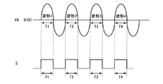
図11は、電力変換装置100Aの動作を説明するための図であり、横方向に時間の経過を示し、縦方向に、交流電圧VA、出力電圧Vo、三角波電圧VB、差分電圧VD’、ゲートパルス信号VSCRのそれぞれを並べて示したものである。
この図に示すように、三角波電圧VBは、交流電圧VAの正相のサイクル期間に対応し、交流電圧VAが負電圧から正電圧に転じる時点を起点として0Vから一定の傾きで増加し、交流電圧VAが正電圧から負電圧に転じる時点でピーク電圧VBPとなった後に0Vとなる波形を有する。各サイクル期間での三角波電圧VBのピーク電圧VBPは一定である。比較回路126は、差分電圧VD’と三角波電圧VBとを比較し、この比較の結果に基づきサイリスタ101の導通タイミングを規定するパルス信号VSCRを生成する。具体的には、三角波電圧VBが電圧VD’よりも大きい区間(VB>VD’)でパルス信号VSCRをハイレベルとし、三角波電圧VBが電圧VD’未満の電圧値の区間ではパルス信号VSCRをローレベルとする。そして、比較回路126は、パルス信号VSCRをサイリスタ101のゲート電極に供給する。
FIG. 11 is a diagram for explaining the operation of the
As shown in this figure, the triangular wave voltage VB corresponds to the positive-phase cycle period of the AC voltage VA, increases from 0 V with a constant slope starting from the time when the AC voltage VA changes from a negative voltage to a positive voltage, When the voltage VA changes from a positive voltage to a negative voltage, it has a waveform that becomes 0 V after the peak voltage VBP is reached. The peak voltage VBP of the triangular wave voltage VB in each cycle period is constant. The
サイリスタ101は、供給されるパルス信号VSCRがハイレベルになった時点でターンオンされる。この後、サイリスタ101は、供給されるパルス信号VSCRがローレベルになると共に交流電圧VAが負電圧に移行すると、サイリスタ101は逆バイアス状態とされてターンオフされる。このように、ゲート制御部120Aは、三角波発生回路125で発生された三角波電圧VBと、増幅回路124から出力された差分電圧VD’とに基づきサイリスタ101の導通状態を制御することにより、電力変換装置100Aの出力電圧Vo(実効値)が目標電圧VTに一致するように制御する。
The
ところで、図9に示す電力変換装置100Aにおいて、この電力変換装置100Aを回転中の発電機10に接続して起動すると、電力変換装置100Aの制御開始時に出力電圧Vo(実効値)が一気に上昇してオーバーシュートを起こすことがある。
By the way, in the
図12は、このような状況の具体例を示す図である。図12に示す例は、発電機10を始動した後、時刻t1のタイミングで、発電機10に電力変換装置100Aを接続し、この電力変換装置100Aを起動した場合の例である。同図に示すように、電力変換装置100Aの制御開始時には差分電圧VD’(=VR’−VT)が小さいので、パルス信号VSCRがハイレベル(ON)となっている期間が長くなる。その結果、バッテリ200に交流電圧VAが供給される時間(充電時間)が長くなる。出力電圧Voはバッテリ200に交流電圧VAが供給されることにより上昇するが、充電時間が長いことと、ゲート制御部120Aにおける制御応答遅れ(出力電圧Voを目標電圧VTに一致させるための制御の遅れ)のために、出力電圧Voが一気に上昇してしまい、図に示すように、出力電圧Voが大きくなりすぎることがある。
FIG. 12 is a diagram showing a specific example of such a situation. The example shown in FIG. 12 is an example when the
なお、図12において交流電圧VAの振幅が変勧しているが、これは発電機の出力が揺らいでいることを示している。一般に、始動時での発電機の出力は図12に示したように揺らぐことが多い。また、波形が歪んでいるのは、サイリスタ101がオン状態のときに、発電機の出力がクランプ状態になっていることを示している。
In FIG. 12, the amplitude of the AC voltage VA is changed, which indicates that the output of the generator is fluctuating. In general, the output of the generator at the start often fluctuates as shown in FIG. Further, the waveform is distorted, indicating that the output of the generator is in the clamped state when the
このオーバーシュートについては、図13(A)に示すように、発電機10の回転速度が大きい場合、すなわち、発電機10の出力電圧及び周波数が高い場合に、この発電機10に電力変換装置100Aを急に接続すると、出力電圧Voに大きなオーバーシュートが発生する。その後、時間の経過とともに、出力電圧Vo(実効値電圧)が次第に目標電圧VTになるように制御される。なお、図13(B)に示すように、発電機10の回転速度が小さい場合、すなわち、発電機10の出力電圧及び周波数が低い場合に、発電機10に電力変換装置100Aを急に接続しても、オーバーシュートは発生しない。
As for this overshoot, as shown in FIG. 13A, when the rotational speed of the
このように、発電機10の高回転中の状態において、電力変換装置100Aを発電機10の出力側に急に接続した場合、電力変換装置100Aの出力電圧が所定の目標電圧VTに制御される状態になるまでに、制御応答遅れのために電力変換装置100Aの出力電圧Voにオーバーシュートが発生するという問題があった。このため、例えば、負荷がランプ負荷の場合は、出力電圧Voが目標電圧VTに一致するように制御が開始されるまでにランプ電圧が高くなり、ランプの発光素子が断線してしまう恐れがあった。また、高出力の発電機では、高回転時に負荷側に大きなラッシュ電流(突入電流)が流れるため、電力変換装置のスイッチング素子(例えば、サイリスタ)の電流容量を大きくする必要があった。
As described above, when the
本発明は、斯かる実情に鑑みなされたものであり、本発明の目的は、回転中の発電機に電力変換装置を接続して起動する際に、この電力変換装置の出力電圧にオーバーシュートが発生することを回避抑できる、電力変換装置及び出力電圧制御方法を提供することにある。 The present invention has been made in view of such circumstances, and an object of the present invention is to overshoot the output voltage of the power converter when the power converter is connected to a rotating generator and started up. An object of the present invention is to provide a power conversion device and an output voltage control method capable of avoiding occurrence.
本発明は、上記課題を解決するためになされたものであり、本発明の電力変換装置は、発電機から出力された交流電圧を入力とし、該交流電圧を整流及び位相制御してバッテリを含む負荷に電圧を供給する電力変換装置であって、前記発電機の出力部と前記負荷との間に接続され、前記交流電圧を整流及び位相制御して前記負荷に電圧を供給するスイッチ部と、前記負荷に供給される電圧を所定の目標電圧に一致するように制御する制御部と、を備え、前記制御部が、前記発電機から出力された交流電圧の各周期に対応したピーク電圧一定の三角波電圧を発生する三角波発生回路と、前記負荷に供給される電圧の実効値を検出しこの実効値電圧の信号を生成する電圧変換回路と、前記実効値電圧と所定の目標電圧との差分電圧に基づき、前記負荷に供給される電圧を前記所定の目標電圧に一致させるように前記スイッチ部の導通状態を制御するための第1の電圧信号を生成する差動増幅回路と、当該装置が起動し制御が開始されるともに、所定の初期電圧から所定の時定数を持って時間の経過とともに次第に電圧レベルが低下する信号であって、該信号の電圧が低下するのに伴い前記負荷に供給される電圧を次第に増加させるように制御する第2の電圧信号を生成するリミット電圧発生回路と、当該装置の起動の際に、前記第1の電圧信号と前記第2の電圧信号とを比較し、前記第1の電圧信号と前記第2の電圧信号との大小関係に基づきいずれか一方の電圧信号を選択し、該選択された信号と前記三角波電圧とを比較し、該選択された信号と該三角波電圧との交差するタイミングを求め、当該タイミングにより前記スイッチ部の導通状態を制御する比較回路と、を備えることを特徴とする。 The present invention has been made to solve the above problems, and a power converter according to the present invention includes an AC voltage output from a generator as an input, and a rectifier and phase control of the AC voltage to include a battery. a power conversion device for supplying a voltage to a load, and which is connected between the output of the generator load, the AC voltage rectifier and phase control that to supply voltage to the load switch unit A control unit that controls the voltage supplied to the load so as to coincide with a predetermined target voltage, and the control unit has a constant peak voltage corresponding to each cycle of the AC voltage output from the generator A triangular wave generating circuit that generates a triangular wave voltage, a voltage conversion circuit that detects an effective value of the voltage supplied to the load and generates a signal of the effective value voltage, and a difference between the effective value voltage and a predetermined target voltage Based on voltage A differential amplifier circuit for generating a first voltage signal for controlling the conduction state of the switch unit so that the voltage supplied to the load coincides with the predetermined target voltage, and the apparatus is activated to start control. In addition, a signal having a predetermined time constant from a predetermined initial voltage and a voltage level gradually decreasing as time elapses, and the voltage supplied to the load gradually increases as the voltage of the signal decreases. A limit voltage generation circuit that generates a second voltage signal that is controlled to be increased, and the first voltage signal and the second voltage signal are compared when the device is activated; One of the voltage signals is selected based on the magnitude relationship between the voltage signal and the second voltage signal, the selected signal is compared with the triangular wave voltage, and the selected signal and the triangular wave voltage are compared. Intersection timing Determined, and wherein the comparison circuit for controlling the conducting state of the switch unit by the timing, that Ru comprising a.
また、本発明の電力変換装置は、前記リミット電圧発生回路が、前記発電機の出力に対して接続され、当該発電機が発電を開始するとともに、コンデンサに充電を開始し、前記装置が起動されると、前記コンデンサに充電した電圧を放電し、徐々に電圧が低下する前記第2の電圧信号を生成することを特徴とする。 Further, in the power conversion device of the present invention, the limit voltage generation circuit is connected to the output of the generator, the generator starts power generation, starts charging the capacitor, and the device is activated. Then, the voltage charged in the capacitor is discharged, and the second voltage signal in which the voltage gradually decreases is generated .
また、本発明の電力変換装置は、前記比較回路は、前記第1の電圧信号と前記第2の電圧信号の信号レベルを比較し、信号レベルの大きい方の信号を選択し、この選択した信号と前記三角波電圧とを比較して交差するタイミングを求め、このタイミングに基づいて前記スイッチ部の導通状態を制御する信号を生成することを特徴とする。 In the power conversion device of the present invention, the comparison circuit compares the signal levels of the first voltage signal and the second voltage signal, selects a signal having a higher signal level, and selects the selected signal. And the triangular wave voltage are compared to obtain a crossing timing, and a signal for controlling the conduction state of the switch unit is generated based on this timing.
また、本発明の電力変換装置は、前記第2の電圧信号の初期値は、当該装置の起動の際に、前記第1の電圧信号よりも大きくなるように設定され、さらに、前記所定の時定数は、当該装置の起動の際に前記負荷に供給される電圧にオーバーシュートが発生しないように設定されることを特徴とする。 In the power conversion device of the present invention, the initial value of the second voltage signal is set to be larger than the first voltage signal when the device is activated, and further, the predetermined time The constant is set so that overshoot does not occur in the voltage supplied to the load when the device is started.
また、本発明の電力変換装置は、前記交流電圧は単相交流電圧であり、前記交流電圧の正相または負相の半波のいずれか一方を前記スイッチ部により整流及び位相制御して前記負荷に直流電圧を印加することを特徴とする。 Further, in the power converter of the present invention, the AC voltage is a single-phase AC voltage, and either the positive phase or the negative phase half wave of the AC voltage is rectified and phase-controlled by the switch unit, and the load A DC voltage is applied to the capacitor.
また、本発明の電力変換装置は、前記スイッチ部がサイリスタ素子であり、前記比較回路は、前記サイリスタの点弧タイミングを制御するパルス信号を出力することを特徴とする。 In the power conversion device of the present invention, the switch unit is a thyristor element, and the comparison circuit outputs a pulse signal for controlling the ignition timing of the thyristor.
また、本発明の出力電圧制御方法は、発電機から出力された交流電圧を入力とし、該交流電圧を整流及び位相制御してバッテリを含む負荷に電圧を供給する電力変換方法において、前記発電機の出力部と前記負荷との間に接続に接続されたスイッチ部を介して、前記発電機から出力された交流電圧を整流及び位相制御して負荷に電圧を供給する手順と、前記負荷に供給される電圧を所定の目標電圧に一致するように制御する制御手順と、を含み、さらに、前記制御手順には、前記発電機から出力された交流電圧の各周期に対応したピーク電圧一定の三角波電圧を発生する三角波発生手順と、前記負荷に供給される電圧の実効値を検出しこの実効値電圧の信号を生成する電圧変換手順と、前記実効値電圧と所定の目標電圧との差分電圧に基づき、前記負荷に供給される電圧を前記所定の目標電圧に一致させるように前記スイッチ部の導通状態を制御するための第1の電圧信号を生成する差動増幅手順と、当該装置が起動し制御が開始されるともに、所定の初期電圧から所定の時定数を持って時間の経過とともに次第に電圧レベルが低下する信号であって、該信号の電圧が低下するのに伴い前記負荷に供給される電圧を次第に増加させるように制御する第2の電圧信号を生成するリミット電圧発生手順と、当該装置の起動の際に、前記第1の電圧信号と前記第2の電圧信号とを比較し、前記第1の電圧信号と前記第2の電圧信号との大小関係に基づきいずれか一方の電圧信号を選択し、該選択された信号と前記三角波電圧とを比較し、該選択された信号と該三角波電圧との交差するタイミングを求め、当該タイミングにより前記スイッチ部の導通状態を制御する比較手順と、を含むことを特徴とする。 Further, the output voltage control method of the present invention is the power conversion method in which the AC voltage output from the generator is input, the AC voltage is rectified and phase-controlled, and the voltage is supplied to the load including the battery. A step of supplying a voltage to the load by rectifying and phase-controlling the AC voltage output from the generator via a switch unit connected between the output unit and the load; and supplying the load to the load A control procedure for controlling the voltage to be matched with a predetermined target voltage, and the control procedure further includes a triangular wave having a constant peak voltage corresponding to each cycle of the AC voltage output from the generator. A triangular wave generating procedure for generating a voltage, a voltage conversion procedure for detecting an effective value of the voltage supplied to the load and generating a signal of the effective value voltage, and a differential voltage between the effective value voltage and a predetermined target voltage Based on A differential amplification procedure for generating a first voltage signal for controlling the conduction state of the switch unit so that the voltage supplied to the load matches the predetermined target voltage; A signal whose voltage level gradually decreases with the passage of time with a predetermined time constant from a predetermined initial voltage, and a voltage supplied to the load as the voltage of the signal decreases. A limit voltage generation procedure for generating a second voltage signal that is controlled to be gradually increased, and the first voltage signal and the second voltage signal are compared when the device is activated, and the first voltage signal is compared. One voltage signal is selected based on the magnitude relationship between the voltage signal and the second voltage signal, the selected signal is compared with the triangular wave voltage, and the selected signal and the triangular wave voltage are compared. Thailand crossing Seek ring, characterized in that it comprises a comparison step of controlling the conduction state of the switch unit by the timing.
本発明の電力変換装置においては、負荷に供給される電圧を所定の目標電圧に一致するように制御する第1の電圧信号と、負荷に供給される電圧を次第に増加させるように制御する第2の電圧信号とを生成する。そして、回転中の発電機に電力変換装置を接続して起動する際には、最初は、第2の電圧信号により出力電圧を緩やかに上昇させるように制御し、出力電圧がある程度立ち上がった後に、出力電圧を第1の電圧信号により目標電圧に一致するように制御する。
これにより、回転中の発電機に電力変換装置を接続して起動する際に、電力変換装置の出力電圧にオーバーシュートが発生することを回避できる。
In the power conversion device of the present invention, the first voltage signal for controlling the voltage supplied to the load to match the predetermined target voltage and the second for controlling the voltage supplied to the load to gradually increase. The voltage signal is generated. And when connecting and starting the power conversion device to the rotating generator, first, the output voltage is controlled to be gradually increased by the second voltage signal, and after the output voltage rises to some extent, The output voltage is controlled by the first voltage signal so as to match the target voltage.
Thereby, when connecting and starting an electric power converter with the rotating generator, it can avoid that an overshoot generate | occur | produces in the output voltage of an electric power converter.
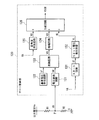
図1に、本実施形態に係る電力変換装置100の構成例を示す。図1において、前述の図9に示す電力変換装置100Aの構成要素と共通する要素には同一符号を付す。
In FIG. 1, the structural example of the
<概要>
図1に示す電力変換装置100の詳細な構成と動作について説明する前に、本発明の特徴部分である、オーバーシュートの抑制動作の概要について説明しておく。
本発明の電力変換装置100では、後述するように、回転中の発電機10に急に接続された場合に、出力電圧Voが一気に上昇してしまうことのないように、ゲート制御部120においてリミット電圧VLを導入する。このリミット電圧VLは、図8に示すように、初期値(図の例では電圧Vz)から、時間の経過とともに次第に減少し、やがて0になる信号である。
<Overview>
Before describing the detailed configuration and operation of the
In the
ゲート制御部120では、リミット電圧VLと差分電圧VD’(出力電圧Voを目標電圧VTに一致させるための制御信号)とを比較し、リミット電圧VLが差分電圧VD’より上にある(電圧レベルが高い)期間、すなわち、時刻t1から時刻t3の期間では、三角波電圧VBとリミット電圧VLとが交差したタイミングで、かつリミット電圧VLが三角波電圧VBよりも大きい区間(VL>VD’)で、パルス信号VSCRをハイレベル(サイリスタ101を導通)とする。それ以外の区間ではローレベルとする。
The
このようにして、電力変換装置100の制御開始時に、最初は、パルス信号VSCRの幅を狭くし(サイリスタ101の導通期間を短くし)、時間の経過とともに次第に広くする(サイリスタ101の導通期間を広くする)。これにより、電力変換装置100の制御開始時において、出力電圧Voを低い電圧から目標電圧VTへとゆっくり上昇させることができる。このため、電力変換装置100の制御開始時に、出力電圧Voにオーバーシュートが発生することを回避できる。
In this way, at the start of control of the
<電力変換装置の全体構成についての説明>
まず、図1を参照して、本実施形態における電力変換装置100の全体構成の例について説明する。
図1に示すように、本電力変換装置100は、発電機のコイル11から出力された交流電圧VAを整流及び位相制御して直流の出力電圧Voに変換し、負荷(バッテリ200及び負荷RL)に電力に供給するものである。電力変換装置100は、サイリスタ101、ゲート制御部120、抵抗R1,R2から構成される。ここで、サイリスタ101は発電機10の出力部とバッテリ200との間に接続されている。具体的には、サイリスタ101のアノードは発電機10のコイル11の一端に接続され、そのカソードにはバッテリ200の正側及び負荷RLの一端に接続されている。バッテリ200の負側及び負荷RLの他端はグランドGに接続されている。
<Description of overall configuration of power conversion device>
First, with reference to FIG. 1, the example of the whole structure of the
As shown in FIG. 1, the
また、サイリスタ101を介してバッテリ200及び負荷RLに供給される出力電圧Voを検出するため、サイリスタ101のカソードとグランドGとの間には、抵抗R1および抵抗R2が直列に接続される。これら抵抗R1と披抗R2との間の接続点Pには、これら抵抗R1と披抗R2とによって出力電圧Voを分圧して得られる電圧VRが現れる。上記接続点Pにはゲート制御部120の入力部が接続され、このゲート制御部120の出力部はサイリスタ101のゲート電極に接続される。
上記構成において、この電力変換装置100は、回転中の発電機10の出力側に急に接続された場合に、出力電圧Voにオーバーシュートが発生することを回避できるように構成されている。
Further, in order to detect the output voltage Vo supplied to the
In the above configuration, the
<ゲート制御部120の構成の説明>
次に、図2を用いてゲート制御部120の全体構成について説明する。
図2は、ゲート制御部120の構成例を示す図である。このゲート制御部120は、図2に示すように、電圧変換回路121、基準電圧発生回路122、差動回路123、増幅回路124、三角波発生回路125、比較回路126、スタート回路131、及びリミット電圧発生回路132を含んで構成される。
<Description of Configuration of
Next, the overall configuration of the
FIG. 2 is a diagram illustrating a configuration example of the
ここで、電圧変換回路121は、上記接続点Pに現れる電圧VRを、その実効値を表す実効値電圧VR’に変換するものであり、その入力部には上記接続点Pが接続されると共に、その出力部は差動回路123の一方の入力部に接続される。この実効値電圧VR’は、上記バッテリ200及び負荷RLに供給される出力電圧Voに対応しており、出力電圧Voの検出値として取り扱われる。
Here, the
基準電圧発生回路122は、バッテリ200の充電(及び負荷RLへ給電)するための目標電圧VTを発生させるものであり、その出力部は差動回路123の他方の入力部に検続される。差動回路123は、実効値電圧VR’と目標電圧VTとの差分電圧VD(=VR’−VT)を生成するものであり、その出力部は増幅回路124の入力部に接続される。
The reference
増幅回路124は、上記差分電圧VDに倍率係数(増幅度)M(>0)を乗じて、差分電圧VDがM倍に増幅された差分電圧VD’を出力するものであり、その出力部は比較回路126の第2の入力部bに接続される。
三角波発生回路125は、上記発電機のコイル11から出力された交流電圧VAの各周期に対応した三角波電圧VBを生成し、生成した三角波電圧VBを比較回路126へ出力する。また、三角波発生回路126は、三角波電圧VBを出力する出力部が、比較回路126の第1の入力部aに接続されている。本実施形態では、三角波電圧VBは、図3の三角波電圧VBに示すように、交流電圧VAの正相のサイクル期間に対応し、交流電圧VAが負電圧から正電圧に転じる時点を起点として0Vから一定の傾きで増加し、交流電圧VAが正電圧から負電圧に転じる時点でピーク電圧VBPとなり、ピーク電圧VBPとなった直後に0Vとなる波形を有する。各サイクル期間での三角波電圧VBのピーク電圧VBPは一定である。この三角波電圧VBの発生メカニズムについては後述する。
The
The triangular
スタート回路131は、リミット電圧発生回路132の入力部と接続される。このスタート回路131は、三角波発生回路125に入力される交流電圧VAを監視しており、交流電圧VAの入力が開始されたタイミングで、リミット電圧発生回路132に対し、リミット電圧VLを発生させるためのスタート信号STを出力する。リミット電圧発生回路132は、スタート信号STが入力されると、リミット電圧VLの出力を開始する。
The
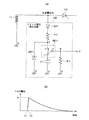
リミット電圧発生回路132は、例えば、図7(A)に示すようなCR回路(後述するコンデンサC11に抵抗R11を用いて電荷を充電し、抵抗R12を用いてコンデンサC11に蓄積された電荷を放電するCR回路)を有して構成される。このCR回路では、サイリスタ101のアノードとグランドGとの間に、ダイオードD11、抵抗R11、スイッチSW11、コンデンサC11がこの順に直列接続される直列回路を有している。この直列回路では、ダイオードD11がアノードからグランドGに向けて順方向接続される。すなわち、ダイオードD11は、アノードがサイリスタ101のアノードに接続され、カソードが接続点Q(スイッチSW11のブレーク接点b)に接続されている。また、抵抗R11とスイッチ11の接続点QからグランドGに向けてツェナーダイオードZD11が逆方向接続される。すなわち、ツェナーダイオードZD11は、アノードがグランドGに接続されて接地され、カソードが接続点Qに接続されている。スイッチSW11は、1c接点を有するスイッチであり、共通接点c1がコンデンサC11の一端(正側)に接続され、ブレーク接点bが上記接続点Qに接続される。また、スイッチSW11のメーク接点aとグランドGとの間に抵抗R12が接続される。そして、スイッチSW11の接点aと抵抗R12の接続点Nから、リミット電圧VLの信号が出力される。
The limit
上記CR回路の構成において、スイッチSW11は、スタート回路131から入力されるスタート信号STにより駆動されるスイッチであり、初期状態においてはOFF状態(共通接点c1とブレーク接点bとが接続された状態)であり、電力変換装置100に交流電圧VAが印加されると、この交流電圧VAにより、ダイオードD11と抵抗R11を通して、直ちにコンデンサC11が充電される(電荷が蓄積される)。このコンデンサC11の充電電圧は、ツェナーダイオードZD11のツェナー電圧Vzより規定される(制限される)電圧となり、また、その充電時定数は、コンデンサC11の静電容量(キャパシタンス)と抵抗R11とで規定される。なお、この充電時定数は、ダイオードD11及びツェナーダイオードZD11に流すことができる許容電流を勘案して、できるだけ短くなるように抵抗R11の抵抗値を設定し、交流電圧VAが印加されると、ダイオードD111及び抵抗R11を介して、直ちにコンデンサC11をツェナー電圧Vzまで急速充電するようにする。
In the configuration of the CR circuit, the switch SW11 is a switch driven by a start signal ST input from the
そして、スタート回路131からスタート信号STが入力されると、スイッチSW11がON状態(共通接点c1と接点aとが接続された状態)になり、リミット電圧発生回路132は、コンデンサC11の充電電位(コンデンサC11の端子間電圧、初期値がツェナー電圧Vz)をリミット電圧VLとして出力する。このコンデンサC11に蓄積された電荷は抵抗R12を通して次第に放電され、すなわち、リミット電圧VLは、コンデンサC11の静電容量と抵抗R12の抵抗値とで規定される放電時定数を持って次第に低下し、いずれ0となる。このように、リミット電圧発生回路132は、コンデンサC11から抵抗R12を介しての放電によって次第に低下する接続点Nの電圧(コンデンサC11の端子間電圧)を、リミット電圧VLとして比較回路126に出力する。
なお、図7(B)は、時間の経過とともに、コンデンサC11の電位(リミット電圧VL)が変化する様子を示しており、この図に示すように、時刻t1において、電力変換装置100に交流電圧VAが印加されると、コンデンサC11の電位が直ちに初期値(ツェナー電圧Vz)の電圧まで充電され、時刻t2において、スタート回路131からスタート信号が入力されると、それ以降、コンデンサC11の電位(リミット電圧VL)が放電により次第に低下し、やがて0となる。
Then, when the start signal ST is input from the
FIG. 7B shows how the potential (limit voltage VL) of the capacitor C11 changes with time. As shown in FIG. 7, the AC voltage is applied to the
比較回路126は、増幅回路124から入力した差分電圧VD’(出力電圧Voを目標電圧VTに一致させるように制御する制御信号)と、リミット電圧発生回路132から入力したリミット電圧VL(出力電圧Voの上昇を制限する信号)とを比較し、この電圧VD’とリミット電圧VLうちの電圧レベルが大きい方の信号を選択し、この選択した電圧(差分電圧VD’またはリミット電圧VL)と三角波電圧VBを比較する。例えば、差分電圧VD’と三角波電圧VBを比較する場合は、差分電圧VD’と三角波電圧VBとの一致点、すなわち差分電圧VD’と三角波電圧VBとが交差するクロス点のタイミングを検出する。このタイミングで、比較回路126は、サイリスタ101の導通タイミングを規定するパルス信号VSCRをハイレベルとし、このパルス信号VSCRをサイリスタ101のゲート電極に出力する。このパルス信号VSCRのハイレベルは、三角波電圧VBが差分電圧VD’よりも大きい区間(VB>VD’)において維持され、それ以外の区間ではローレベルとなる。
The
同様に、リミット電圧VLと三角波電圧VBを比較する場合は、リミット電圧VLと三角波電圧VBとの一致点、すなわちリミット電圧VLと三角波電圧VBとが交差するクロス点のタイミングを検出する。このタイミングで、比較回路126は、サイリスタ101の導通タイミングを規定するパルス信号VSCRをハイレベルとし、このパルス信号VSCRをサイリスタ101のゲート電極に出力する。このパルス信号VSCRのハイレベルは、三角波電圧VBがリミット電圧VLよりも大きい区間(VB>VL)において維持され、それ以外の区間ではローレベルとなる。
Similarly, when the limit voltage VL and the triangular wave voltage VB are compared, the coincidence point between the limit voltage VL and the triangular wave voltage VB, that is, the timing of the cross point where the limit voltage VL and the triangular wave voltage VB intersect is detected. At this timing, the
パルス信号VSCRをゲート電極に入力するサイリスタ101は、パルス信号VSCRがハイレベルになった時点でターンオンされる。この後、パルス信号VSCRがローレベルになると共に交流電圧VAが負電圧に移行すると、サイリスタ101は逆バイアス状態とされてターンオフされる。即ち、サイリスタ101は、三角波電圧VBが、差分電圧VD’及びリミット電圧VLの両方よりも高い区間においてオン状態とされ、それ以外の区間ではオフ状態とされる。このように、ゲート制御部120は、三角波発生回路125で発生された三角波電圧VBと、増幅回路124から出力された差分電圧VD’と、リミット電圧発生回路132から出力されたリミット電圧VLと、に基づきサイリスタ101の導通状態を制御する。
The
<電力変換装置100の通常時の動作についての説明>
次に、図3から図6を参照して、本電力変換装置100の通常時(定常時)の動作について説明する。なお、通常動作時には、リミット電圧VLは0Vまで低下しており、ここでは、比較回路126において、差分電圧VD’と三角波電圧VBのみが比較される例について説明する。なお、回転中の発電機10に電力変換装置100を接続した場合の起動時の動作については後述する。
<Description of Normal Operation of
Next, with reference to FIG. 3 to FIG. 6, the normal operation (normal operation) of the
図3は、電力変換装置100における各部の波形を示す図であり、横方向に時間の経過を示し、縦方向に、交流電圧VA、三角波電圧VB及び差分電圧VD’、パルス信号VSCRのそれぞれを並べて示したものである。
以下、図3を参照して、電力変換装置100の通常時の動作について説明する。ゲート制御部120内の差動回路123では、基準電圧発生回路122で発生された目標電圧VTと、電圧変換回路121から出力された電圧VR’とを入力し、これらの差分電圧VDを生成する。増幅回路124は差分電圧VDをM倍に増幅して、比較回路126に電圧VD’(=M×VD)を供給する。
FIG. 3 is a diagram illustrating waveforms of the respective units in the
Hereinafter, a normal operation of the
比較回路126では、リミット電圧VLより差分電圧VD’が大きいため、差分電圧VD’と三角波電圧VBとを比較し、この比較の結果に基づきサイリスタ101の導通タイミングを規定するパルス信号VSCRを生成する。そして、比較回路126は、三角波電圧VBが差分電圧VD’よりも高い区間(VB>VD’)でパルス信号VSCRをハイレベルとし、三角波電圧VBが差分電圧VD’よりも低い区間(VB<VD’)でパルス信号VSCRをローレベルとして、このパルス信号VSCRをサイリスタ101のゲート電極に供給する。すなわち、サイリスタ101は、三角波電圧VBが差分電圧VD’よりも高い区間(VB>VD’)においてオン状態とされ、それ以外の区間ではオフ状態とされる。このように、ゲート制御部120は、三角波発生回路125で発生された三角波電圧VBと、増幅回路124から出力された差分電圧VD’とに基づきサイリスタ101の導通状態を制御する。
In the
ここで、サイリスタ101のオン状態の区間、すなわち三角波電圧VBが差分電圧VD’よりも高い期間は差分電圧VD’のレベルに依存し、この差分電圧VD’のレベルは、目標電圧VTに対する出力電圧Voのレベルに依存する。従って、出力電圧Voが高ければ、電圧VD’のレベルも高くなり、三角波電圧VBが差分電圧VD’より高くなる期間が減少し、サイリスタ101がオン状態となる期間が減少する。この結果、出力電圧Voが目標電圧VTに向けて低下する。
Here, the period in which the
逆に、出力電圧Voが低ければ、差分電圧VD’のレベルも低くなり、この結果、三角波電圧VBが差分電圧VD’よりも高い期間が増加し、サイリスタ101がオン状態となる期間が増加する。この結果、出力電圧Voが目標電圧VTに向けて上昇する。このように、発電機の交流電圧VAの各周期において、出力電圧Voが目標電圧VTに安定するようにサイリスタ101の導通期間が制御される。
On the contrary, if the output voltage Vo is low, the level of the differential voltage VD ′ is also low. As a result, the period in which the triangular wave voltage VB is higher than the differential voltage VD ′ increases, and the period in which the
以上により発電磯10の回転数が低い場合を説明したが、発電機10の回転数が高い場合には、図3(B)に示すように、発電機10が出力する交流電圧VAの振幅が大きくなると共に、その周波数も高くなるので、三角波電圧VBの上昇レートが大きくなるが、その他の点では、上述の図3(A)に示す発電機10の回転数が低い場合と同様であり、出力電圧Voの実効値が目標電圧VTに安定するようにサイリスタ101のゲート制御が実施される。
The case where the rotational speed of the
次に、図4及び図5を参照して、三角波発生回路125における三角波電圧VBの発生メカニズムを説明する。
一般には発電機10が出力する交流電圧の周波数は急激に変化しないので、1サイクル前の波形と現在のサイクルの波形はほとんど同じと考えることができる。例えば、図4において、波形2が現在のサイクルの波形だとすれば、波形2の半周期T2と、その1サイクル前の波形1の半周期T1とはほとんど同じである。
Next, the generation mechanism of the triangular wave voltage VB in the triangular
In general, since the frequency of the AC voltage output from the
上述の特性を利用して、次の手順により三角波電圧VBを生成する。
(手順1)図4に示すように、波形1のサイクルにおいて、発電機が出力する交流電圧VAから方形波Sを生成する。この波形1に対応する方形波Sの半周期は、波形1のサイクルにおける交流電圧VAの半周期T1と一致する。
(手順2)続いて、方形波Sの半周期T1の時間をカウントする。
(手順3)続いて、半周期T1の時間のカウント数を所定の分解能nで除算して、時間t1(=T1/n)を得る。ここで、分解能nは、三角波電圧VBのスロープの滑らかさを規定する量であり、分解能nが高い程、三角波電圧VBのスロープが滑らかになる。
(手順4)続いて、三角波電圧VBのピーク電圧VBPを所定の分解能nで除算して、電圧v1(=VBP/n)を得る。
(手順5)続いて、図5(B)に示すように、次のサイクルの波形2の立ち上がりタイミング(T2をカウントし始めるタイミング)で、上記電圧v1だけ三角波電圧VBを上昇させ、この三角波電圧VBを上記時間t1の間だけ維持する。
Using the above characteristics, the triangular wave voltage VB is generated by the following procedure.
(Procedure 1) As shown in FIG. 4, in the cycle of
(Procedure 2) Subsequently, the time of the half cycle T1 of the square wave S is counted.
(Procedure 3) Subsequently, the time t1 (= T1 / n) is obtained by dividing the count of the time of the half cycle T1 by a predetermined resolution n. Here, the resolution n is an amount that defines the smoothness of the slope of the triangular wave voltage VB. The higher the resolution n, the smoother the slope of the triangular wave voltage VB.
(Procedure 4) Subsequently, the peak voltage VBP of the triangular wave voltage VB is divided by a predetermined resolution n to obtain a voltage v1 (= VBP / n).
(Procedure 5) Subsequently, as shown in FIG. 5B, the triangular wave voltage VB is increased by the voltage v1 at the rising timing of
(手順6)同じ波形2のサイクルにおいて、上記時間t1が経過したタイミングで上記電圧v1だけ三角波電圧VBを更に上昇させ、これを全都でn回繰り返すと、図5(B)に示すような階段状の波形が得られ、波形2のサイクルに対応する三角波電圧のスロープ部分に相当する階段状の波形が得られる。分解能nの値を大きくすれば、階段状の波形が滑らかになり、一層良好な三角波を得ることができる。
以上の手順により、1サイクル前の交流電圧VAの波形を用いて、交流電圧VAの各周期に対応した三角波電圧であって、ピーク電圧VBPが一定の電圧波形を生成する。
(Procedure 6) In the cycle of the
With the above procedure, a waveform of a triangular wave voltage corresponding to each cycle of the AC voltage VA and having a constant peak voltage VBP is generated using the waveform of the AC voltage VA one cycle before.
上述の三角波電圧の発生メカニズムを利用した三角波発生回路125は、本電力変換装置においてサイリスタ101の導通タイミングを制御するための三角波電圧VBを生成するものであって、例えば、カウンタ部と、除算部と、波形生成部とから構成することができる。ここで、カウンタ部は、発電機が出力する第1サイクルの交流電圧波形の半周期の時間(図4の例えば波形1のサイクルにおける時間T1)をカウントするものである。除算部は、上記カウンタ部によるカウント数を所定の分解能n(所定値)で除算するものである。波形生成部は、第1サイクル後の第2サイクル(図4の例えば波形2のサイクル)において上記第1サイクルでの除算部の除算結果で示される時間t1の経過ごとに所定電圧v1だけ上昇する階段状の電圧波形を生成するものである。この階段状の電圧波形は上記三角波電圧VBの波形として出力される。
The triangular
<増幅回路124を導入することの技術的意味>
次に、図6を参照して、増幅回路124を導入することの技術的意味を説明する。
図6(A)は、増幅回路124の増幅度である倍率係数Mを「1」とした場合の三角波電圧VBと差分電圧VD’(=VD)との相対的な開係を示している。図6(A)において、区間W1は、三角波電圧VBが差分電圧VD’を上回る期間、すなわちサイリスタ101がオン状態に制御される期間を示す。また、図6(B)は、倍率係数Mを「2」に設定した場合の三角波電圧VBと差分電圧VD’(=2×VD)との相対的な関係を示している。図6(B)に示すように倍率係数Mを「2」に設定して差分電圧VDを2倍に増幅すると、図6(A)に示す区間W1と比較して、サイリスタ101のオン状態に対応する区間W2の変動量(VD’の変動量)が2倍になり、これにより、出力電圧Voの変動量に対してパルス信号VSCRの応答量(感度)が2倍になる。
<Technical meaning of introducing the
Next, the technical meaning of introducing the
FIG. 6A shows a relative relationship between the triangular wave voltage VB and the differential voltage VD ′ (= VD) when the magnification factor M, which is the amplification degree of the
このことは、図6(C)に示すように、倍率係数Mが「1」のときの差分電圧VD’(=VD)に対して三角波電圧のピーク電圧が相対的に半分(VB/2)になることと等価であり、出力電圧Voの制御幅VWが半分になることを意味している。従って、増幅回路124を導入して、差分電圧VDをM倍に増幅することにより、出力電圧Voの制御幅VWが相対的にM分の1に小さくなるため、出力電圧Voを精度よく目標電圧VTに制御できるようになる。
As shown in FIG. 6C, the peak voltage of the triangular wave voltage is relatively half (VB / 2) relative to the differential voltage VD ′ (= VD) when the magnification factor M is “1”. It means that the control width VW of the output voltage Vo is halved. Therefore, by introducing the
ここで、三角波電圧VBの高さH(=ピーク電圧VP)と、倍率係数Mと、目標電圧VTと、出力電圧Voの制御幅VWとの間には、Wが、VTからVT+(H/M)の範囲の値となる関係が存在する。従って、本電力変換装置を実施する場合、所望の制御幅Wと目標電圧VTとに応じて、上記開係を満足するように三角波電圧VBの高さHと倍率係数Mとを適切に設定すればよい。 Here, between the height H (= peak voltage VP) of the triangular wave voltage VB, the magnification factor M, the target voltage VT, and the control width VW of the output voltage Vo, W is changed from VT to VT + (H / There is a relationship that is a value in the range of M). Therefore, when implementing this power converter, according to the desired control width W and the target voltage VT, the height H and the magnification factor M of the triangular wave voltage VB are appropriately set so as to satisfy the above open relationship. That's fine.
<電力変換装置が回転中の発電機に接続された場合の動作についての説明>
次に、発電機10の回転中に、この発電機10の出力側に電力変換装置100が接続された場合の動作、すなわち、電力変換装置100の起動時の動作について説明する。
<Description of operation when power conversion device is connected to rotating generator>
Next, an operation when the
図8は、回転中の発電機に電力変換装置が接続された場合の起動時の動作について説明するための図である。図8に示す例は、前述の図12と同様に、時刻t1が、回転中の発電機10に電力変換装置100が接続されたタイミングである。以下、図8を参照して、電力変換装置100の起動時の動作について説明する。
時刻t1において、電力変換装置100が発電機10に接続されると、この電力変換装置100は起動し制御動作を開始する。そして、発電機10から交流電圧VAが入力されると、スタート回路131はこれを検出し、スタート信号STを生成してリミット電圧発生回路132に出力する。リミット電圧発生回路132は、スタート回路131からスタート信号STを入力すると、リミット電圧VLの出力動作を開始する。
FIG. 8 is a diagram for explaining an operation at the time of startup when a power conversion device is connected to a rotating generator. In the example shown in FIG. 8, the time t1 is the timing when the
When the
このリミット電圧発生回路132から出力されるリミット電圧VLは、例えば、図7に例示したCR回路により生成される。このリミット電圧VLは起動時(時刻t1)における初期値Vzから、次第に低下し、やがて0になる信号である。一方、差分電圧VD’(=M×(VR’−VT))については、起動直後はバッテリ200及び負荷RLにまだ電力が供給されていないため、出力電圧Vo(バッテリ200の電圧)及び電圧VR’(出力電圧Voの検出値)は目標電圧VTよりも低いため、この差分電圧VD’は負値をとる。このため、リミット電圧VLの方が差分電圧VD’よりも大きく、比較回路126では、リミット電圧VLを選択し、このリミット電圧VLと三角波電圧VBとを比較する。
そして、三角波電圧VBがリミット電圧VLよりも大きくなる区間(VB>VL)でパルス信号VSCRをハイレベル(サイリスタ101を導通)にする。なお、起動直後においては、リミット電圧VLは初期値Vzであり電圧レベルが高いため、三角波電圧VBがリミット電圧VLよりも大きくなる区間(パルス信号VSCRがハイレベルなる期間)は短く、出力電圧Vo及び差分電圧VD’も僅かにだけ上昇する。
The limit voltage VL output from the limit
Then, the pulse signal VSCR is set to the high level (the
その後、時間の経過とともにリミット電圧VLの電圧値が低下することにより、三角波電圧VBがリミット電圧VLよりも大きくなる区間(パルス信号VSCRがハイレベルとなる区間)が次第に増大する。そして、時刻t2において、差分電圧VD’が正の値に転じるが、この時刻t2においても、リミット電圧VLの方が差分電圧VD’よりも大きいため、リミット電圧VLの方が選択される。
時刻t2からさらに時間が経過し、リミット電圧VLがさらに低下し、出力電圧Vo及び差分電圧VD’がさらに増加すると、やがて、時刻t3において、差分電圧VD’の方がリミット電圧VLよりも大きくなる。この時刻t3以降は、リミット電圧VLはさらに低下していくため、常に差分電圧VD’の方がリミット電圧VLよりも大きくなる。このため、時刻t3以降においては、比較回路126は、差分電圧VD’を選択し、この差分電圧VD’と三角波電圧VBを比較することによりパルス信号VSCRを生成するようになる。従って、時刻t3以降は、電力変換装置100では、差分電圧VD’を用いて出力電圧Voを目標電圧VTに一致させる通常の制御動作に移行することになる。
Thereafter, as the voltage value of the limit voltage VL decreases with the passage of time, a section in which the triangular wave voltage VB becomes larger than the limit voltage VL (a section in which the pulse signal VSCR becomes high level) gradually increases. Then, the differential voltage VD ′ turns to a positive value at time t2, but the limit voltage VL is selected because the limit voltage VL is larger than the differential voltage VD ′ at time t2.
As time elapses further from time t2 and the limit voltage VL further decreases and the output voltage Vo and the differential voltage VD ′ further increase, the differential voltage VD ′ eventually becomes larger than the limit voltage VL at time t3. . After this time t3, the limit voltage VL further decreases, so the differential voltage VD ′ is always greater than the limit voltage VL. Therefore, after time t3, the
このように、比較回路126では、時刻t1から時刻t3までの間は、リミット電圧VLを選択し、このリミット電圧VLと三角波電圧VBとを比較してパルス信号VSCRを生成する。このリミット電圧VLは、最初は電圧レベルが高く、次第に小さくなる信号であるため、最初は、パルス信号VSCRがハイレベルとなる期間が短く、リミット電圧VLが低下するに従い、パルス信号VSCRがハイレベルとなる期間が長くなる。すなわち、時間の経過とともにリミット電圧VLが低下し、これに伴い、出力電圧Voが緩やかに増加することになる。
As described above, the
このように、電力変換装置100では、回転中の発電機10に接続して起動する際に、出力電圧Voの上昇のさせ方をリミット電圧VLにより制御することができる。このため、出力電圧Voが一気に上昇してオーバーシュートが発生することを回避できる。また、リミット電圧VLの初期値及び時定数(例えば、図7に示すCR回路における放電時定数)制御することにより、出力電圧Voの適切な上昇を図れる。
As described above, in the
以上、本発明の実施形態について説明したが、ここで、本発明と上記実施形態の対応関係について補足して説明しておく。
上記実施形態において、本発明における電力変換装置は、電力変換装置100が対応し、本発明における発電機は、発電機10が対応し、本発明におけるスイッチ部は、サイリスタ101が対応する。また、本発明における制御部は、ゲート制御部120が対応する。また、本発明における電圧変換回路は、電圧変換回路121が対応し、本発明における基準電圧発生回路は、基準電圧発生回路122が対応し、本発明における差動増幅回路は、差動回路123と増幅回路124とが対応し、本発明における三角波発生回路は三角波発生回路125が対応する。また、本発明における比較回路は、比較回路126が対応し、本発明におけるスタート回路は、スタート回路131が対応し、本発明におけるリミット電圧発生回路は、リミット電圧発生回路132が対応する。
また、本発明における負荷に供給される電圧は、出力電圧Voが対応し、本発明における第1の電圧信号は、差分電圧VD’が対応し、本発明における第2の電圧信号は、リミット電圧VLが対応し、本発明における初期電圧はツェナー電圧Vzが対応する。また、本発明における目標電圧は目標電圧VTが対応し、本発明における第2の電圧信号の初期電圧は、ツェナー電圧Vzが対応する。
The embodiment of the present invention has been described above. Here, the correspondence between the present invention and the above embodiment will be supplementarily described.
In the said embodiment, the power converter device in this invention respond | corresponds to the
The voltage supplied to the load in the present invention corresponds to the output voltage Vo, the first voltage signal in the present invention corresponds to the differential voltage VD ′, and the second voltage signal in the present invention represents the limit voltage. The initial voltage in the present invention corresponds to the Zener voltage Vz. The target voltage in the present invention corresponds to the target voltage VT, and the initial voltage of the second voltage signal in the present invention corresponds to the Zener voltage Vz.
(1)そして、上記実施形態において、電力変換装置100は、発電機10から出力された交流電圧VAを入力とし、該交流電圧VAを整流及び位相制御してバッテリを含む負荷(バッテリ200及び負荷RL)に出力電圧Voを供給する電力変換装置100であって、発電機10の出力部と負荷との間に接続されるサイリスタ101と、負荷に供給される出力電圧Voを所定の目標電圧VTに一致するように制御するゲート制御部120と、を備え、このゲート制御部120では、負荷(バッテリ200及び負荷RL)に供給される出力電圧Voと所定の目標電圧VTとの差分電圧の信号であって上記負荷に供給される出力電圧Voを所定の目標電圧VTに一致させるように制御する第1の電圧信号(差分電圧VD’)を生成すると共に、当該装置100の起動の際に、所定の初期電圧(ツェナー電圧Vz)から時間の経過とともに次第に電圧が低下する信号であって該信号の電圧が低下するのに伴い上記負荷に供給される出力電圧Voを次第に増加させるように制御する第2の電圧信号(リミット電圧VL)を生成し、当該装置100の起動の際に、第1の電圧信号(差分電圧VD’)と第2の電圧信号(リミット電圧VL)との大小関係に基づきいずれか一方の電圧信号を選択し、この選択した電圧信号に基づきサイリスタ101の導通状態を制御する。
(1) In the above embodiment, the
このような構成の電力変換装置100では、負荷(バッテリ200及び負荷RL)に供給される出力電圧Voを所定の目標電圧VTに一致するように制御する第1の電圧信号(差分電圧VD’)を生成する。また、当該装置100が起動し制御が開始されるともに初期電圧(ツェナー電圧Vz)から時間の経過とともに次第に電圧レベルが低下する第2の電圧信号(リミット電圧VL)を生成する。そして、回転中の発電機10に電力変換装置100を接続して当該装置100を起動する際には、最初は、第2の電圧信号(リミット電圧VL)を選択し、この第2の電圧信号(リミット電圧VL)が次第に低下するのに伴い、出力電圧Voを初期値(例えば、バッテリ200の初期電圧)から緩やかに上昇させるように制御する。そして、出力電圧Voがある程度上昇し(目標電圧VTに近づき)、第1の電圧信号(差分電圧VD’)が第2の電圧信号(リミット電圧VL)よりも大きくなったときは、これ以降、第1の電圧信号(差分電圧VD’)を選択し、出力電圧Voを第1の電圧信号(差分電圧VD’)により目標電圧VTに一致するように制御する。
これにより、回転中の発電機10に電力変換装置100を接続して起動する際に、電力変換装置100の出力電圧Voにオーバーシュートが発生することを回避できる。
In the
Thereby, when connecting and starting the
(2)また、上記実施形態において、電力変換装置100は、発電機10の出力部と負荷(バッテリ200及び負荷RL)との間に接続に接続され、交流電圧VAを整流及び位相制御して負荷に出力電圧Voを供給するサイリスタ101と、発電機10から出力された交流電圧VAの各周期に対応したピーク電圧一定の三角波電圧VBを発生する三角波発生回路125と、負荷に供給される出力電圧Voの実効値を検出しこの実効値電圧VR’の信号を生成する電圧変換回路121と、実効値電圧VR’と所定の目標電圧VTとの差分電圧VDに基づき、サイリスタ101の導通状態を制御するための第1の電圧信号(差分電圧VD’)を生成する差動増幅回路(差動回路123及び増幅回路124)と、当該装置100が起動し制御が開始されるともに所定の初期電圧(ツェナー電圧Vz)から所定の時定数を持って次第に電圧レベルが低下する第2の電圧信号(リミット電圧VL)を生成するリミット電圧発生回路132と、第1の電圧信号(差分電圧VD’)と第2の電圧信号(リミット電圧VL)とを比較し、大小関係によりいずれか一方の信号を選択し、該選択された信号と三角波電圧VBとの比較結果に基づいて、サイリスタ101の導通状態を制御する比較回路126と、を備える。
(2) Moreover, in the said embodiment, the
このような構成の電力変換装置100では、図8に示すように、三角波発生回路125により、三角波電圧VBを、交流電圧VAと同位相でピーク値一定で生成する。また、電圧変換回路121により、出力電圧Voの実効値電圧VR’の信号を生成し、差動回路123及び増幅回路124により、実効値電圧VR’と目標電圧VTとの差分電圧VD’(=M×(VR’−VT))の信号を、第1の電圧信号(差分電圧VD’)として生成する。また、リミット電圧発生回路132により、出力電圧Voの上昇を制御するための第2の電圧信号(リミット電圧VL)を生成する。このリミット電圧VLは、制御が開始されると共に初期値(ツェナー電圧Vz)から時間の経過とともに次第にレベルが低下し、やがて0になる信号である。
In the
そして、比較回路126では、リミット電圧VLと差分電圧VD’とを比較し、リミット電圧VLの方が差分電圧VD’より電圧レベルが高い区間(VL>VD’)、すなわち、時刻t1から時刻t3の期間では、三角波電圧VBとリミット電圧VLとが交差したタイミングで、かつリミット電圧VLが三角波電圧VBよりも大きい区間(VB>VL)で、パルス信号VSCRをハイレベル(サイリスタ101を導通)とする。それ以外の区間ではローレベルとする。このようにして、電力変換装置100の制御開始時に、最初は、パルス信号VSCRの幅を狭くし(サイリスタ101の導通期間を短くし)、時間の経過とともに、次第に広くする(サイリスタ101の導通期間を長くする)ことにより、出力電圧Voを緩やかに上昇させる。
The
これにより、回転中の発電機10に電力変換装置100を接続して起動する際に、出力電圧Voを低い電圧から目標電圧VTへと緩やかに上昇させることができる。すなわち、電力変換装置100が起動し制御を開始する際に、出力電圧Voにオーバーシュートが発生することを回避できる。このため、例えば、ランプ(照明用のランプ)にオーバーシュートによる高電圧が印加されることを抑止でき、高電圧印加によるランプ切れの発生を抑止できる。また、リミット電圧VLの初期値(ツェナー電圧Vz)や、電圧レベルが低下する時間(時定数)を設定することにより、出力電圧Voの上昇のさせ方(例えば、上昇時間等)を制御することができる。さらには、電力変換装置100の起動の際に、発電機10から負荷側に大きなラッシュ電流(突入電流)が流れることを抑止できる。
Thereby, when connecting and starting the
(3)また、上記実施形態において、比較回路126は、第1の電圧信号(差分電圧VD’)と第2の電圧信号(リミット電圧VL)の信号レベルを比較し、信号レベルの大きい方の信号を選択し、この選択した信号と三角波電圧VBとを比較して交差するタイミングを求め、このタイミングに基づいてサイリスタ101の導通状態を制御する信号を生成する。
このような構成の電力変換装置では、比較回路126が、リミット電圧VLと差分電圧VD’とを比較し、信号レベルの大きい方の信号を選択して三角波電圧VBと比較する。例えば、電力変換装置100の起動時には、第2の電圧信号(リミット電圧VL)の方が第1の電圧信号(差分電圧VD’)よりも大きいので、比較回路126では、第2の電圧信号(リミット電圧VL)を選択して三角波電圧VBと比較する。そして、三角波電圧VBと第2の電圧信号(リミット電圧VL)とが交差したタイミングで、かつリミット電圧VLが三角波電圧VBよりも大きい区間(VB>VL)で、パルス信号VSCRをハイレベル(サイリスタ101を導通)とする。それ以外の区間ではローレベルとする。このようにして、電力変換装置100の制御開始時に、最初は、パルス信号VSCRの幅を狭くし(サイリスタ101の導通期間を短くし)、時間の経過とともに、次第に広くする(サイリスタ101の導通期間を長くする)ことにより、出力電圧Voを緩やかに上昇させることができる。
これにより、回転中の発電機10に電力変換装置100を接続して起動する際に、出力電圧Voを低い電圧から目標電圧VTへとゆっくり上昇させることができる。すなわち、電力変換装置100の制御開始時に、出力電圧Voにオーバーシュートが発生することを回避できる。
(3) In the above-described embodiment, the
In the power conversion device having such a configuration, the
Thereby, when connecting and starting the
(4)また、上記実施形態において、第2の電圧信号(リミット電圧VL)の初期値(ツェナー電圧Vz)は、当該装置100の起動の際に、第1の電圧信号(差分電圧VD‘)よりも大きくなるように設定され、さらに、上記時定数(第2の電圧信号(リミット電圧VL)の電圧レベルを次第に低下させる時定数)は、当該装置100の起動の際に負荷に供給される出力電圧Voにオーバーシュートが発生しないように設定される。
これにより、回転中の発電機10に電力変換装置100を接続して起動した場合に、第2の電圧信号(リミット電圧VL)により出力電圧Voの上昇のさせ方(例えば、上昇時間等)を制御できる。このため、電力変換装置100の出力電圧Voにオーバーシュートが発生することを回避できる。
(4) In the above embodiment, the initial value (zener voltage Vz) of the second voltage signal (limit voltage VL) is the first voltage signal (difference voltage VD ′) when the
Thus, when the
(5)また、上記実施形態において、交流電圧VAは単相交流電圧であり、交流電圧VAの正相または負相の半波のいずれか一方をサイリスタ101により整流及び位相制御して負荷に直流電圧を印加する。
これにより、車両(例えば、2輪車)に搭載された単相発電機(回転中の発電機)に、電力変換装置100を接続する場合に、電力変換装置100の出力電圧Voにオーバーシュートが発生することを回避できる。
(5) In the above embodiment, the AC voltage VA is a single-phase AC voltage, and either the positive phase or the negative phase half-wave of the AC voltage VA is rectified and phase-controlled by the
As a result, when the
(6)また、上記実施形態において、電力変換装置100はサイリスタ101を用いて構成されており、比較回路126は、サイリスタ101の点弧タイミングを制御するパルス信号VCSRを出力する。
これにより、サイリスタ101を用いた電力変換装置100において、この電力変換装置100を、回転中の発電機10に接続して起動した場合に、出力電圧Voにオーバーシュートが発生することを回避できる。
(6) Moreover, in the said embodiment, the
Thereby, in the
以上、本発明の実施の形態について説明したが、本発明の電力変換装置は、上述の図示例にのみ限定されるものではなく、本発明の要旨を逸脱しない範囲内において種々変更を加え得ることは勿論である。 As mentioned above, although embodiment of this invention was described, the power converter device of this invention is not limited only to the above-mentioned example of illustration, A various change can be added in the range which does not deviate from the summary of this invention. Of course.
例えば、図1に示す実施形態では、発電機から出力される交流電力の正相成分についてのみサイリスタ101を介して負荷に電力を供給するものとし、発電機の出力を半波整流する場合を説明したが、これに限定されることなく、発電機からら出力された交流電力の負相成分について同様に半波整流することにより、全波整流するように構成することもできる。また、図1に示した実施形態では、単相の交流電力を変換するものとしたが、多相の交流電力に対しても適用することができる。
For example, in the embodiment shown in FIG. 1, only the positive phase component of the AC power output from the generator is supplied to the load via the
また、例えば、図1に示す実施形態では、電圧変換回路121において出力電圧Voの実効値を求める例について説明したが、本発明は、出力電圧Voの平均値を算出する場合にも同様に適用できるものである。出力電圧Voの平均値を生成するための構成としては公知技術を利用できる。
For example, in the embodiment shown in FIG. 1, the example in which the effective value of the output voltage Vo is obtained in the
10 発電機
11 コイル
100,100A 電力変換装置
101 サイリスタ
120,120A ゲート制御部
121 電圧変換回路
122 基準電圧発生回路
123 差動回路
124 増幅回路
125 三角波発生回路
126 比較回路
131 スタート回路
132 リミット電圧発生回路
200 バッテリ
C11 コンデンサ
D11 ダイオード
R1,R2,R11,R12 抵抗
SW11 スイッチ
VB 三角波電圧
VD 差分電圧
VD’ 差分電圧(第1の電圧信号)
VL リミット電圧(第2の電圧信号)
Vo 出力電圧
VR’ 実効値電圧(実効値の検出電圧)
VSCR ゲートパルス信号
VT 目標電圧
Vz ツェナー電圧
ZD11 ツェナーダイオード
DESCRIPTION OF
VL limit voltage (second voltage signal)
Vo output voltage VR 'RMS voltage (effective value detection voltage)
VSCR Gate pulse signal VT Target voltage Vz Zener voltage ZD11 Zener diode
Claims (7)
前記発電機の出力部と前記負荷との間に接続され、前記交流電圧を整流及び位相制御して前記負荷に電圧を供給するスイッチ部と、
前記負荷に供給される電圧を所定の目標電圧に一致するように制御する制御部と、
を備え、
前記制御部が、
前記発電機から出力された交流電圧の各周期に対応したピーク電圧一定の三角波電圧を発生する三角波発生回路と、
前記負荷に供給される電圧の実効値を検出しこの実効値電圧の信号を生成する電圧変換回路と、
前記実効値電圧と所定の目標電圧との差分電圧に基づき、前記負荷に供給される電圧を前記所定の目標電圧に一致させるように前記スイッチ部の導通状態を制御するための第1の電圧信号を生成する差動増幅回路と、
当該装置が起動し制御が開始されるともに、所定の初期電圧から所定の時定数を持って時間の経過とともに次第に電圧レベルが低下する信号であって、該信号の電圧が低下するのに伴い前記負荷に供給される電圧を次第に増加させるように制御する第2の電圧信号を生成するリミット電圧発生回路と、
当該装置の起動の際に、前記第1の電圧信号と前記第2の電圧信号とを比較し、前記第1の電圧信号と前記第2の電圧信号との大小関係に基づきいずれか一方の電圧信号を選択し、該選択された信号と前記三角波電圧とを比較し、該選択された信号と該三角波電圧との交差するタイミングを求め、当該タイミングにより前記スイッチ部の導通状態を制御する比較回路と、
を備える
ことを特徴とする電力変換装置。 An AC converter output from a generator is used as an input, and the AC converter supplies a voltage to a load including a battery by rectifying and phase controlling the AC voltage,
A switch unit that to supply voltage to the connected, the load the AC voltage rectified and with phase control between the output of the generator load,
A control unit that controls the voltage supplied to the load to match a predetermined target voltage;
With
The control unit is
A triangular wave generating circuit for generating a triangular wave voltage having a constant peak voltage corresponding to each cycle of the AC voltage output from the generator;
A voltage conversion circuit that detects an effective value of the voltage supplied to the load and generates a signal of the effective value voltage; and
Based on a differential voltage between the effective value voltage and a predetermined target voltage, a first voltage signal for controlling the conduction state of the switch unit so that the voltage supplied to the load matches the predetermined target voltage. A differential amplifier circuit for generating
The device is activated and the control is started, and a signal having a predetermined time constant from a predetermined initial voltage and a voltage level gradually decreasing as time elapses, and as the voltage of the signal decreases, A limit voltage generating circuit that generates a second voltage signal that is controlled so as to gradually increase the voltage supplied to the load;
When the device is activated, the first voltage signal and the second voltage signal are compared, and one of the voltages is determined based on the magnitude relationship between the first voltage signal and the second voltage signal. A comparison circuit that selects a signal, compares the selected signal with the triangular wave voltage, finds a timing at which the selected signal and the triangular wave voltage intersect, and controls the conduction state of the switch unit according to the timing When,
Power conversion apparatus characterized by Ru with a.
前記発電機の出力に対して接続され、当該発電機が発電を開始するとともに、コンデンサに充電を開始し、前記装置が起動されると、前記コンデンサに充電した電圧を放電し、徐々に電圧が低下する前記第2の電圧信号を生成するConnected to the output of the generator, the generator starts power generation, starts charging the capacitor, and when the device is activated, discharges the voltage charged in the capacitor and gradually increases the voltage. Generating the second voltage signal to decrease
ことを特徴とする請求項1に記載の電力変換装置。The power conversion apparatus according to claim 1.
前記第1の電圧信号と前記第2の電圧信号の信号レベルを比較し、信号レベルの大きい方の信号を選択し、この選択した信号と前記三角波電圧とを比較して交差するタイミングを求め、このタイミングに基づいて前記スイッチ部の導通状態を制御する信号を生成する
ことを特徴とする請求項1または請求項2に記載の電力変換装置。 The comparison circuit is
Compare the signal levels of the first voltage signal and the second voltage signal, select the signal with the higher signal level, compare the selected signal with the triangular wave voltage, and determine the timing of crossing, The power conversion device according to claim 1 or 2, wherein a signal for controlling a conduction state of the switch unit is generated based on the timing.
さらに、前記所定の時定数は、当該装置の起動の際に前記負荷に供給される電圧にオーバーシュートが発生しないように設定される
ことを特徴とする請求項1または請求項2に記載の電力変換装置。 The initial value of the second voltage signal is set to be larger than the first voltage signal when the device is activated,
The power according to claim 1 or 2, wherein the predetermined time constant is set so that overshoot does not occur in the voltage supplied to the load when the device is activated. Conversion device.
ことを特徴とする請求項1または請求項2に記載の電力変換装置。 The AC voltage is a single-phase AC voltage, and the DC voltage is applied to the load by rectifying and phase-controlling either the positive phase or the negative phase half wave of the AC voltage by the switch unit. The power conversion device according to claim 1 or 2.
前記比較回路は、前記サイリスタの点弧タイミングを制御するパルス信号を出力する
ことを特徴とする請求項1または請求項2に記載の電力変換装置。 The switch part is a thyristor element;
The power converter according to claim 1 , wherein the comparison circuit outputs a pulse signal that controls an ignition timing of the thyristor.
前記発電機の出力部と前記負荷との間に接続に接続されたスイッチ部を介して、前記発電機から出力された交流電圧を整流及び位相制御して負荷に電圧を供給する手順と、
前記負荷に供給される電圧を所定の目標電圧に一致するように制御する制御手順と、
を含み、
さらに、前記制御手順には、
前記発電機から出力された交流電圧の各周期に対応したピーク電圧一定の三角波電圧を発生する三角波発生手順と、
前記負荷に供給される電圧の実効値を検出しこの実効値電圧の信号を生成する電圧変換手順と、
前記実効値電圧と所定の目標電圧との差分電圧に基づき、前記負荷に供給される電圧を前記所定の目標電圧に一致させるように前記スイッチ部の導通状態を制御するための第1の電圧信号を生成する差動増幅手順と、
当該装置が起動し制御が開始されるともに、所定の初期電圧から所定の時定数を持って時間の経過とともに次第に電圧レベルが低下する信号であって、該信号の電圧が低下するのに伴い前記負荷に供給される電圧を次第に増加させるように制御する第2の電圧信号を生成するリミット電圧発生手順と、
当該装置の起動の際に、前記第1の電圧信号と前記第2の電圧信号とを比較し、前記第1の電圧信号と前記第2の電圧信号との大小関係に基づきいずれか一方の電圧信号を選択し、該選択された信号と前記三角波電圧とを比較し、該選択された信号と該三角波電圧との交差するタイミングを求め、当該タイミングにより前記スイッチ部の導通状態を制御する比較手順と、
を含むことを特徴とする出力電圧制御方法。 In a power conversion method for supplying an AC voltage output from a generator as an input, rectifying and phase-controlling the AC voltage and supplying a voltage to a load including a battery,
A procedure for supplying a voltage to the load by rectifying and phase-controlling the AC voltage output from the generator via a switch unit connected in a connection between the output unit of the generator and the load;
A control procedure for controlling the voltage supplied to the load to match a predetermined target voltage;
Including
Furthermore, the control procedure includes
A triangular wave generation procedure for generating a triangular wave voltage with a constant peak voltage corresponding to each cycle of the AC voltage output from the generator;
A voltage conversion procedure for detecting an effective value of the voltage supplied to the load and generating a signal of the effective value voltage;
Based on a differential voltage between the effective value voltage and a predetermined target voltage, a first voltage signal for controlling the conduction state of the switch unit so that the voltage supplied to the load matches the predetermined target voltage. A differential amplification procedure to generate
The device is activated and the control is started, and a signal having a predetermined time constant from a predetermined initial voltage and a voltage level gradually decreasing as time elapses, and as the voltage of the signal decreases, A limit voltage generation procedure for generating a second voltage signal for controlling the voltage supplied to the load to gradually increase;
When the device is activated, the first voltage signal and the second voltage signal are compared, and one of the voltages is determined based on the magnitude relationship between the first voltage signal and the second voltage signal. A comparison procedure for selecting a signal, comparing the selected signal with the triangular wave voltage, obtaining a timing at which the selected signal and the triangular wave voltage intersect, and controlling the conduction state of the switch unit according to the timing When,
Output voltage control method, which comprises a.
Priority Applications (1)
| Application Number | Priority Date | Filing Date | Title |
|---|---|---|---|
| JP2010280839A JP5658996B2 (en) | 2010-12-16 | 2010-12-16 | Power converter and output voltage control method |
Applications Claiming Priority (1)
| Application Number | Priority Date | Filing Date | Title |
|---|---|---|---|
| JP2010280839A JP5658996B2 (en) | 2010-12-16 | 2010-12-16 | Power converter and output voltage control method |
Publications (2)
| Publication Number | Publication Date |
|---|---|
| JP2012130196A JP2012130196A (en) | 2012-07-05 |
| JP5658996B2 true JP5658996B2 (en) | 2015-01-28 |
Family
ID=46646604
Family Applications (1)
| Application Number | Title | Priority Date | Filing Date |
|---|---|---|---|
| JP2010280839A Active JP5658996B2 (en) | 2010-12-16 | 2010-12-16 | Power converter and output voltage control method |
Country Status (1)
| Country | Link |
|---|---|
| JP (1) | JP5658996B2 (en) |
Family Cites Families (3)
| Publication number | Priority date | Publication date | Assignee | Title |
|---|---|---|---|---|
| JPH0710177B2 (en) * | 1990-10-19 | 1995-02-01 | 富士電気化学株式会社 | Switching regulator |
| JP3303015B2 (en) * | 1995-02-01 | 2002-07-15 | いすゞ自動車株式会社 | Voltage control device for magnet generator |
| WO2007102601A1 (en) * | 2006-03-09 | 2007-09-13 | Shindengen Electric Manufacturing Co., Ltd. | Power conversion device and method, and triangular wave generation circuit |
-
2010
- 2010-12-16 JP JP2010280839A patent/JP5658996B2/en active Active
Also Published As
| Publication number | Publication date |
|---|---|
| JP2012130196A (en) | 2012-07-05 |
Similar Documents
| Publication | Publication Date | Title |
|---|---|---|
| CN108809100B (en) | System and method for regulating output current of power conversion system | |
| JP4718598B2 (en) | Power conversion apparatus and method, and triangular wave generation circuit | |
| KR100823922B1 (en) | Apparatus and method for supplying dc power source | |
| US20160380552A1 (en) | Input voltage detection circuit and power supply including the same | |
| US9491819B2 (en) | Hysteretic power factor control method for single stage power converters | |
| JP6272691B2 (en) | Amplitude normalization circuit, power supply device and electronic device | |
| JP5624952B2 (en) | Control device and control method | |
| JP6279080B2 (en) | Power converter | |
| US20050219866A1 (en) | Switching power source apparatus | |
| KR20070093635A (en) | Apparatus and method for supplying dc power source | |
| WO2003071666A1 (en) | Switching power source apparatus | |
| JP5452543B2 (en) | Control circuit and control method | |
| US20130135911A1 (en) | Ac-dc converter | |
| WO2001048904A1 (en) | Portable generator | |
| TW201218605A (en) | AC/DC converter, AC/DC conversion method, and controller for controlling voltage conversion | |
| JP6793227B2 (en) | Alternator and its rectifier | |
| JP5658996B2 (en) | Power converter and output voltage control method | |
| JP2000341957A (en) | Power supply unit | |
| US11245328B2 (en) | Integrated circuit and power supply circuit | |
| JP2009213280A (en) | Power factor correcting circuit | |
| EP3499705B1 (en) | Creeping discharge element drive device and creeping discharge element drive method | |
| JP5658995B2 (en) | Power converter and output voltage control method | |
| JP5674447B2 (en) | Voltage detection circuit and voltage conversion circuit | |
| CN111435810B (en) | Alternator and rectifier device | |
| WO2017106870A1 (en) | A flyback converter and a method for controlling a flyback converter |
Legal Events
| Date | Code | Title | Description |
|---|---|---|---|
| A621 | Written request for application examination |
Free format text: JAPANESE INTERMEDIATE CODE: A621 Effective date: 20130516 |
|
| A977 | Report on retrieval |
Free format text: JAPANESE INTERMEDIATE CODE: A971007 Effective date: 20140312 |
|
| A131 | Notification of reasons for refusal |
Free format text: JAPANESE INTERMEDIATE CODE: A131 Effective date: 20140408 |
|
| A521 | Written amendment |
Free format text: JAPANESE INTERMEDIATE CODE: A523 Effective date: 20140609 |
|
| TRDD | Decision of grant or rejection written | ||
| A01 | Written decision to grant a patent or to grant a registration (utility model) |
Free format text: JAPANESE INTERMEDIATE CODE: A01 Effective date: 20141104 |
|
| A61 | First payment of annual fees (during grant procedure) |
Free format text: JAPANESE INTERMEDIATE CODE: A61 Effective date: 20141201 |
|
| R150 | Certificate of patent (=grant) or registration of utility model |
Ref document number: 5658996 Country of ref document: JP Free format text: JAPANESE INTERMEDIATE CODE: R150 |