JP5656611B2 - Semiconductor device and solid-state imaging device - Google Patents
Semiconductor device and solid-state imaging device Download PDFInfo
- Publication number
- JP5656611B2 JP5656611B2 JP2010283771A JP2010283771A JP5656611B2 JP 5656611 B2 JP5656611 B2 JP 5656611B2 JP 2010283771 A JP2010283771 A JP 2010283771A JP 2010283771 A JP2010283771 A JP 2010283771A JP 5656611 B2 JP5656611 B2 JP 5656611B2
- Authority
- JP
- Japan
- Prior art keywords
- conductive member
- wiring
- pad
- circuit
- pads
- Prior art date
- Legal status (The legal status is an assumption and is not a legal conclusion. Google has not performed a legal analysis and makes no representation as to the accuracy of the status listed.)
- Active
Links
- 239000004065 semiconductor Substances 0.000 title claims description 108
- 238000003384 imaging method Methods 0.000 title description 23
- 230000002093 peripheral effect Effects 0.000 claims description 18
- 238000006243 chemical reaction Methods 0.000 claims description 15
- 239000000463 material Substances 0.000 claims description 8
- 239000004020 conductor Substances 0.000 claims description 3
- 239000010410 layer Substances 0.000 description 39
- 239000000758 substrate Substances 0.000 description 18
- 230000003287 optical effect Effects 0.000 description 13
- 230000000694 effects Effects 0.000 description 9
- 238000010586 diagram Methods 0.000 description 8
- 230000006870 function Effects 0.000 description 8
- 230000015654 memory Effects 0.000 description 7
- 229910021420 polycrystalline silicon Inorganic materials 0.000 description 7
- 229920005591 polysilicon Polymers 0.000 description 7
- 239000011229 interlayer Substances 0.000 description 6
- 238000002955 isolation Methods 0.000 description 5
- 238000002161 passivation Methods 0.000 description 5
- RYGMFSIKBFXOCR-UHFFFAOYSA-N Copper Chemical compound [Cu] RYGMFSIKBFXOCR-UHFFFAOYSA-N 0.000 description 2
- 229910052782 aluminium Inorganic materials 0.000 description 2
- XAGFODPZIPBFFR-UHFFFAOYSA-N aluminium Chemical compound [Al] XAGFODPZIPBFFR-UHFFFAOYSA-N 0.000 description 2
- 229910052802 copper Inorganic materials 0.000 description 2
- 239000010949 copper Substances 0.000 description 2
- 238000005516 engineering process Methods 0.000 description 2
- 238000004519 manufacturing process Methods 0.000 description 2
- 229910052581 Si3N4 Inorganic materials 0.000 description 1
- VYPSYNLAJGMNEJ-UHFFFAOYSA-N Silicium dioxide Chemical compound O=[Si]=O VYPSYNLAJGMNEJ-UHFFFAOYSA-N 0.000 description 1
- XUIMIQQOPSSXEZ-UHFFFAOYSA-N Silicon Chemical compound [Si] XUIMIQQOPSSXEZ-UHFFFAOYSA-N 0.000 description 1
- 230000008901 benefit Effects 0.000 description 1
- 230000008859 change Effects 0.000 description 1
- 239000011810 insulating material Substances 0.000 description 1
- 239000012212 insulator Substances 0.000 description 1
- 239000011159 matrix material Substances 0.000 description 1
- 229910052751 metal Inorganic materials 0.000 description 1
- 239000002184 metal Substances 0.000 description 1
- 238000000034 method Methods 0.000 description 1
- 238000004806 packaging method and process Methods 0.000 description 1
- 230000008569 process Effects 0.000 description 1
- 230000009467 reduction Effects 0.000 description 1
- 229910052710 silicon Inorganic materials 0.000 description 1
- 239000010703 silicon Substances 0.000 description 1
- HQVNEWCFYHHQES-UHFFFAOYSA-N silicon nitride Chemical compound N12[Si]34N5[Si]62N3[Si]51N64 HQVNEWCFYHHQES-UHFFFAOYSA-N 0.000 description 1
- 229910052814 silicon oxide Inorganic materials 0.000 description 1
- WFKWXMTUELFFGS-UHFFFAOYSA-N tungsten Chemical compound [W] WFKWXMTUELFFGS-UHFFFAOYSA-N 0.000 description 1
- 229910052721 tungsten Inorganic materials 0.000 description 1
- 239000010937 tungsten Substances 0.000 description 1
Images


Classifications
-
- H—ELECTRICITY
- H01—ELECTRIC ELEMENTS
- H01L—SEMICONDUCTOR DEVICES NOT COVERED BY CLASS H10
- H01L23/00—Details of semiconductor or other solid state devices
- H01L23/52—Arrangements for conducting electric current within the device in operation from one component to another, i.e. interconnections, e.g. wires, lead frames
- H01L23/522—Arrangements for conducting electric current within the device in operation from one component to another, i.e. interconnections, e.g. wires, lead frames including external interconnections consisting of a multilayer structure of conductive and insulating layers inseparably formed on the semiconductor body
-
- H—ELECTRICITY
- H01—ELECTRIC ELEMENTS
- H01L—SEMICONDUCTOR DEVICES NOT COVERED BY CLASS H10
- H01L24/00—Arrangements for connecting or disconnecting semiconductor or solid-state bodies; Methods or apparatus related thereto
- H01L24/01—Means for bonding being attached to, or being formed on, the surface to be connected, e.g. chip-to-package, die-attach, "first-level" interconnects; Manufacturing methods related thereto
- H01L24/02—Bonding areas ; Manufacturing methods related thereto
- H01L24/04—Structure, shape, material or disposition of the bonding areas prior to the connecting process
- H01L24/06—Structure, shape, material or disposition of the bonding areas prior to the connecting process of a plurality of bonding areas
-
- H—ELECTRICITY
- H01—ELECTRIC ELEMENTS
- H01L—SEMICONDUCTOR DEVICES NOT COVERED BY CLASS H10
- H01L27/00—Devices consisting of a plurality of semiconductor or other solid-state components formed in or on a common substrate
- H01L27/14—Devices consisting of a plurality of semiconductor or other solid-state components formed in or on a common substrate including semiconductor components sensitive to infrared radiation, light, electromagnetic radiation of shorter wavelength or corpuscular radiation and specially adapted either for the conversion of the energy of such radiation into electrical energy or for the control of electrical energy by such radiation
- H01L27/144—Devices controlled by radiation
- H01L27/146—Imager structures
- H01L27/14601—Structural or functional details thereof
- H01L27/14603—Special geometry or disposition of pixel-elements, address-lines or gate-electrodes
-
- H—ELECTRICITY
- H01—ELECTRIC ELEMENTS
- H01L—SEMICONDUCTOR DEVICES NOT COVERED BY CLASS H10
- H01L2224/00—Indexing scheme for arrangements for connecting or disconnecting semiconductor or solid-state bodies and methods related thereto as covered by H01L24/00
- H01L2224/01—Means for bonding being attached to, or being formed on, the surface to be connected, e.g. chip-to-package, die-attach, "first-level" interconnects; Manufacturing methods related thereto
- H01L2224/02—Bonding areas; Manufacturing methods related thereto
- H01L2224/0212—Auxiliary members for bonding areas, e.g. spacers
- H01L2224/02122—Auxiliary members for bonding areas, e.g. spacers being formed on the semiconductor or solid-state body
- H01L2224/02163—Auxiliary members for bonding areas, e.g. spacers being formed on the semiconductor or solid-state body on the bonding area
- H01L2224/02165—Reinforcing structures
- H01L2224/02166—Collar structures
-
- H—ELECTRICITY
- H01—ELECTRIC ELEMENTS
- H01L—SEMICONDUCTOR DEVICES NOT COVERED BY CLASS H10
- H01L2224/00—Indexing scheme for arrangements for connecting or disconnecting semiconductor or solid-state bodies and methods related thereto as covered by H01L24/00
- H01L2224/01—Means for bonding being attached to, or being formed on, the surface to be connected, e.g. chip-to-package, die-attach, "first-level" interconnects; Manufacturing methods related thereto
- H01L2224/02—Bonding areas; Manufacturing methods related thereto
- H01L2224/04—Structure, shape, material or disposition of the bonding areas prior to the connecting process
- H01L2224/04042—Bonding areas specifically adapted for wire connectors, e.g. wirebond pads
-
- H—ELECTRICITY
- H01—ELECTRIC ELEMENTS
- H01L—SEMICONDUCTOR DEVICES NOT COVERED BY CLASS H10
- H01L2224/00—Indexing scheme for arrangements for connecting or disconnecting semiconductor or solid-state bodies and methods related thereto as covered by H01L24/00
- H01L2224/01—Means for bonding being attached to, or being formed on, the surface to be connected, e.g. chip-to-package, die-attach, "first-level" interconnects; Manufacturing methods related thereto
- H01L2224/02—Bonding areas; Manufacturing methods related thereto
- H01L2224/04—Structure, shape, material or disposition of the bonding areas prior to the connecting process
- H01L2224/05—Structure, shape, material or disposition of the bonding areas prior to the connecting process of an individual bonding area
- H01L2224/0554—External layer
- H01L2224/05541—Structure
- H01L2224/05548—Bonding area integrally formed with a redistribution layer on the semiconductor or solid-state body
-
- H—ELECTRICITY
- H01—ELECTRIC ELEMENTS
- H01L—SEMICONDUCTOR DEVICES NOT COVERED BY CLASS H10
- H01L2224/00—Indexing scheme for arrangements for connecting or disconnecting semiconductor or solid-state bodies and methods related thereto as covered by H01L24/00
- H01L2224/01—Means for bonding being attached to, or being formed on, the surface to be connected, e.g. chip-to-package, die-attach, "first-level" interconnects; Manufacturing methods related thereto
- H01L2224/02—Bonding areas; Manufacturing methods related thereto
- H01L2224/04—Structure, shape, material or disposition of the bonding areas prior to the connecting process
- H01L2224/05—Structure, shape, material or disposition of the bonding areas prior to the connecting process of an individual bonding area
- H01L2224/0554—External layer
- H01L2224/0556—Disposition
- H01L2224/05567—Disposition the external layer being at least partially embedded in the surface
-
- H—ELECTRICITY
- H01—ELECTRIC ELEMENTS
- H01L—SEMICONDUCTOR DEVICES NOT COVERED BY CLASS H10
- H01L2224/00—Indexing scheme for arrangements for connecting or disconnecting semiconductor or solid-state bodies and methods related thereto as covered by H01L24/00
- H01L2224/01—Means for bonding being attached to, or being formed on, the surface to be connected, e.g. chip-to-package, die-attach, "first-level" interconnects; Manufacturing methods related thereto
- H01L2224/02—Bonding areas; Manufacturing methods related thereto
- H01L2224/04—Structure, shape, material or disposition of the bonding areas prior to the connecting process
- H01L2224/06—Structure, shape, material or disposition of the bonding areas prior to the connecting process of a plurality of bonding areas
- H01L2224/061—Disposition
- H01L2224/0612—Layout
- H01L2224/0615—Mirror array, i.e. array having only a reflection symmetry, i.e. bilateral symmetry
- H01L2224/06151—Mirror array, i.e. array having only a reflection symmetry, i.e. bilateral symmetry being uniform, i.e. having a uniform pitch across the array
-
- H—ELECTRICITY
- H01—ELECTRIC ELEMENTS
- H01L—SEMICONDUCTOR DEVICES NOT COVERED BY CLASS H10
- H01L2224/00—Indexing scheme for arrangements for connecting or disconnecting semiconductor or solid-state bodies and methods related thereto as covered by H01L24/00
- H01L2224/01—Means for bonding being attached to, or being formed on, the surface to be connected, e.g. chip-to-package, die-attach, "first-level" interconnects; Manufacturing methods related thereto
- H01L2224/02—Bonding areas; Manufacturing methods related thereto
- H01L2224/04—Structure, shape, material or disposition of the bonding areas prior to the connecting process
- H01L2224/06—Structure, shape, material or disposition of the bonding areas prior to the connecting process of a plurality of bonding areas
- H01L2224/061—Disposition
- H01L2224/0612—Layout
- H01L2224/0615—Mirror array, i.e. array having only a reflection symmetry, i.e. bilateral symmetry
- H01L2224/06154—Mirror array, i.e. array having only a reflection symmetry, i.e. bilateral symmetry covering only portions of the surface to be connected
- H01L2224/06155—Covering only the peripheral area of the surface to be connected, i.e. peripheral arrangements
-
- H—ELECTRICITY
- H01—ELECTRIC ELEMENTS
- H01L—SEMICONDUCTOR DEVICES NOT COVERED BY CLASS H10
- H01L2224/00—Indexing scheme for arrangements for connecting or disconnecting semiconductor or solid-state bodies and methods related thereto as covered by H01L24/00
- H01L2224/01—Means for bonding being attached to, or being formed on, the surface to be connected, e.g. chip-to-package, die-attach, "first-level" interconnects; Manufacturing methods related thereto
- H01L2224/02—Bonding areas; Manufacturing methods related thereto
- H01L2224/04—Structure, shape, material or disposition of the bonding areas prior to the connecting process
- H01L2224/06—Structure, shape, material or disposition of the bonding areas prior to the connecting process of a plurality of bonding areas
- H01L2224/061—Disposition
- H01L2224/0612—Layout
- H01L2224/0615—Mirror array, i.e. array having only a reflection symmetry, i.e. bilateral symmetry
- H01L2224/06157—Mirror array, i.e. array having only a reflection symmetry, i.e. bilateral symmetry with specially adapted redistribution layers [RDL]
- H01L2224/06159—Mirror array, i.e. array having only a reflection symmetry, i.e. bilateral symmetry with specially adapted redistribution layers [RDL] being disposed in different wiring levels, i.e. resurf layout
-
- H—ELECTRICITY
- H01—ELECTRIC ELEMENTS
- H01L—SEMICONDUCTOR DEVICES NOT COVERED BY CLASS H10
- H01L2224/00—Indexing scheme for arrangements for connecting or disconnecting semiconductor or solid-state bodies and methods related thereto as covered by H01L24/00
- H01L2224/01—Means for bonding being attached to, or being formed on, the surface to be connected, e.g. chip-to-package, die-attach, "first-level" interconnects; Manufacturing methods related thereto
- H01L2224/02—Bonding areas; Manufacturing methods related thereto
- H01L2224/04—Structure, shape, material or disposition of the bonding areas prior to the connecting process
- H01L2224/06—Structure, shape, material or disposition of the bonding areas prior to the connecting process of a plurality of bonding areas
- H01L2224/061—Disposition
- H01L2224/0612—Layout
- H01L2224/0616—Random array, i.e. array with no symmetry
- H01L2224/06164—Random array, i.e. array with no symmetry covering only portions of the surface to be connected
- H01L2224/06165—Covering only the peripheral area of the surface to be connected, i.e. peripheral arrangements
-
- H—ELECTRICITY
- H01—ELECTRIC ELEMENTS
- H01L—SEMICONDUCTOR DEVICES NOT COVERED BY CLASS H10
- H01L2224/00—Indexing scheme for arrangements for connecting or disconnecting semiconductor or solid-state bodies and methods related thereto as covered by H01L24/00
- H01L2224/01—Means for bonding being attached to, or being formed on, the surface to be connected, e.g. chip-to-package, die-attach, "first-level" interconnects; Manufacturing methods related thereto
- H01L2224/02—Bonding areas; Manufacturing methods related thereto
- H01L2224/04—Structure, shape, material or disposition of the bonding areas prior to the connecting process
- H01L2224/06—Structure, shape, material or disposition of the bonding areas prior to the connecting process of a plurality of bonding areas
- H01L2224/061—Disposition
- H01L2224/0612—Layout
- H01L2224/0616—Random array, i.e. array with no symmetry
- H01L2224/06167—Random array, i.e. array with no symmetry with specially adapted redistribution layers [RDL]
- H01L2224/06169—Random array, i.e. array with no symmetry with specially adapted redistribution layers [RDL] being disposed in different wiring levels, i.e. resurf layout
-
- H—ELECTRICITY
- H01—ELECTRIC ELEMENTS
- H01L—SEMICONDUCTOR DEVICES NOT COVERED BY CLASS H10
- H01L23/00—Details of semiconductor or other solid state devices
- H01L23/52—Arrangements for conducting electric current within the device in operation from one component to another, i.e. interconnections, e.g. wires, lead frames
- H01L23/522—Arrangements for conducting electric current within the device in operation from one component to another, i.e. interconnections, e.g. wires, lead frames including external interconnections consisting of a multilayer structure of conductive and insulating layers inseparably formed on the semiconductor body
- H01L23/528—Geometry or layout of the interconnection structure
- H01L23/5286—Arrangements of power or ground buses
-
- H—ELECTRICITY
- H01—ELECTRIC ELEMENTS
- H01L—SEMICONDUCTOR DEVICES NOT COVERED BY CLASS H10
- H01L2924/00—Indexing scheme for arrangements or methods for connecting or disconnecting semiconductor or solid-state bodies as covered by H01L24/00
- H01L2924/0001—Technical content checked by a classifier
- H01L2924/00014—Technical content checked by a classifier the subject-matter covered by the group, the symbol of which is combined with the symbol of this group, being disclosed without further technical details
-
- H—ELECTRICITY
- H01—ELECTRIC ELEMENTS
- H01L—SEMICONDUCTOR DEVICES NOT COVERED BY CLASS H10
- H01L2924/00—Indexing scheme for arrangements or methods for connecting or disconnecting semiconductor or solid-state bodies as covered by H01L24/00
- H01L2924/01—Chemical elements
- H01L2924/01013—Aluminum [Al]
-
- H—ELECTRICITY
- H01—ELECTRIC ELEMENTS
- H01L—SEMICONDUCTOR DEVICES NOT COVERED BY CLASS H10
- H01L2924/00—Indexing scheme for arrangements or methods for connecting or disconnecting semiconductor or solid-state bodies as covered by H01L24/00
- H01L2924/01—Chemical elements
- H01L2924/01029—Copper [Cu]
-
- H—ELECTRICITY
- H01—ELECTRIC ELEMENTS
- H01L—SEMICONDUCTOR DEVICES NOT COVERED BY CLASS H10
- H01L2924/00—Indexing scheme for arrangements or methods for connecting or disconnecting semiconductor or solid-state bodies as covered by H01L24/00
- H01L2924/01—Chemical elements
- H01L2924/01033—Arsenic [As]
-
- H—ELECTRICITY
- H01—ELECTRIC ELEMENTS
- H01L—SEMICONDUCTOR DEVICES NOT COVERED BY CLASS H10
- H01L2924/00—Indexing scheme for arrangements or methods for connecting or disconnecting semiconductor or solid-state bodies as covered by H01L24/00
- H01L2924/01—Chemical elements
- H01L2924/01074—Tungsten [W]
-
- H—ELECTRICITY
- H01—ELECTRIC ELEMENTS
- H01L—SEMICONDUCTOR DEVICES NOT COVERED BY CLASS H10
- H01L2924/00—Indexing scheme for arrangements or methods for connecting or disconnecting semiconductor or solid-state bodies as covered by H01L24/00
- H01L2924/10—Details of semiconductor or other solid state devices to be connected
- H01L2924/11—Device type
- H01L2924/13—Discrete devices, e.g. 3 terminal devices
- H01L2924/1304—Transistor
- H01L2924/1306—Field-effect transistor [FET]
- H01L2924/13091—Metal-Oxide-Semiconductor Field-Effect Transistor [MOSFET]
Description
本発明は半導体装置の配線技術に関するものであり、とりわけ固体撮像装置の配線技術に関する。 The present invention relates to wiring technology for semiconductor devices, and more particularly to wiring technology for solid-state imaging devices.
半導体装置は半導体チップ外部からの信号が入力される入力パッドと、外部へ信号を出力するための出力パッドとを有している。 The semiconductor device has an input pad for inputting a signal from the outside of the semiconductor chip and an output pad for outputting a signal to the outside.
特許文献1は、半導体装置におけるパッド及び配線のレイアウトを開示している。特許文献1の図1に記載された半導体装置は、内部回路の周りを完全に囲むように配された内部回路用電源配線(4a、4b)を有する。そして、内部回路用の第1電源パッド(8a、8b)が、この内部回路用電源配線と一体化して形成されている。さらに、チップの外周部に、内部回路用の第2電源パッド(7a、7b)が配される。 Patent Document 1 discloses a layout of pads and wirings in a semiconductor device. The semiconductor device described in FIG. 1 of Patent Document 1 has internal circuit power supply wires (4a, 4b) arranged so as to completely surround the internal circuit. The first power pads (8a, 8b) for the internal circuit are formed integrally with the power wiring for the internal circuit. Further, second power supply pads (7a, 7b) for internal circuits are arranged on the outer periphery of the chip.
このようなレイアウトにおいては、配線が互いに交差する必要がある。具体的には、第2電源パッドから内部回路に電源電圧を供給する電源配線が、内部回路用電源配線と交差する必要がある。そのため、特許文献1では、第2電源パッドから内部回路に電源を供給する配線が、第1電源パッドと平面的に重なったレイアウトが開示されている。 In such a layout, the wirings need to cross each other. Specifically, the power supply wiring that supplies the power supply voltage from the second power supply pad to the internal circuit needs to intersect the internal circuit power supply wiring. Therefore, Patent Document 1 discloses a layout in which wiring for supplying power from the second power supply pad to the internal circuit overlaps the first power supply pad in a planar manner.
一般に半導体装置は、一枚のウエハから得ることができる半導体チップの数(チップ収量)を多くすることが望まれる。このため、同一の機能、目的を実現するデバイスをできるだけ小さい面積の半導体チップに配することが求められる。 In general, a semiconductor device is desired to increase the number of semiconductor chips (chip yield) that can be obtained from one wafer. For this reason, it is required to arrange devices that realize the same function and purpose on a semiconductor chip having the smallest possible area.
本発明者らは、パッドよりも半導体チップの内周部に配された回路間の電気的接続において、パッドと配線との位置関係によって半導体チップ面積を縮小できることを見出した。 The inventors have found that the area of the semiconductor chip can be reduced by the positional relationship between the pad and the wiring in the electrical connection between the circuits arranged in the inner peripheral portion of the semiconductor chip rather than the pad.
本発明は上記知見に基づいてなされたものであり、本発明は、半導体チップ面積を縮小可能な半導体装置を提供することを目的とする。 The present invention has been made based on the above findings, and an object of the present invention is to provide a semiconductor device capable of reducing the area of a semiconductor chip.
本発明に係る半導体装置は、入力パッドと出力パッドとを含む複数のパッドと、第1回路部及び第2回路部と、前記第1回路部の出力ノードと前記第2回路部の入力ノードとを電気的に接続するための配線と、が配された半導体チップを有する半導体装置であって、前記第1回路部及び前記第2回路部は前記複数のパッドよりも前記半導体チップの内周部に配され、前記配線は、導電部材を含んで構成され、前記導電部材の少なくとも一部が、前記複数のパッドに含まれる少なくとも一つのパッドと重なって配されたことを特徴とする。 A semiconductor device according to the present invention includes a plurality of pads including an input pad and an output pad, a first circuit unit and a second circuit unit, an output node of the first circuit unit, and an input node of the second circuit unit. And a wiring for electrically connecting the semiconductor chip, wherein the first circuit portion and the second circuit portion are inner peripheral portions of the semiconductor chip rather than the plurality of pads. The wiring is configured to include a conductive member, and at least a part of the conductive member is arranged to overlap at least one pad included in the plurality of pads.
本発明の別の側面に係る半導体装置は、入力パッドと出力パッドとを含む複数のパッドと、回路部と、前記複数のパッドに含まれる第1パッドと前記回路部のノードとを電気的に接続するための配線と、が配された半導体チップを有する半導体装置であって、前記回路部は前記複数のパッドよりも前記半導体チップの内周部に配され、前記配線は、導電部材を含んで構成され、前記導電部材の一部が、前記複数のパッドに含まれる第2パッドと重なって配されたことを特徴とする。 A semiconductor device according to another aspect of the present invention electrically connects a plurality of pads including an input pad and an output pad, a circuit unit, a first pad included in the plurality of pads, and a node of the circuit unit. And a wiring for connecting the semiconductor chip, wherein the circuit portion is arranged in an inner peripheral portion of the semiconductor chip rather than the plurality of pads, and the wiring includes a conductive member. A part of the conductive member is arranged so as to overlap the second pad included in the plurality of pads.
本発明によれば、半導体装置のチップ面積を縮小することが可能となる。 According to the present invention, the chip area of a semiconductor device can be reduced.
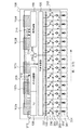
図1を用いて本発明の要部の説明を行う。図1において、100は半導体装置である。半導体装置100の最外周の太線は半導体チップの端を示している。
The main part of the present invention will be described with reference to FIG. In FIG. 1,
本発明は半導体装置に関する。本明細書において、半導体装置とは、デバイスが配された半導体基板、該半導体基板がパッケージされた部品、または、該部品が実装された装置を意味する。デバイスが配された半導体基板であって、パッケージするためのサイズに切断されたものを半導体チップ、あるいは単にチップと呼ぶ。ただし、実際に切断されていなくても、半導体基板のうちパッケージするために切り離されるべき一部分が半導体チップである。また、固体撮像装置とは、半導体装置のうち、撮像用途の装置を意味する。 The present invention relates to a semiconductor device. In this specification, a semiconductor device means a semiconductor substrate on which devices are arranged, a component on which the semiconductor substrate is packaged, or an apparatus on which the component is mounted. A semiconductor substrate on which devices are arranged and cut to a package size is called a semiconductor chip or simply a chip. However, even if it is not actually cut, a part of the semiconductor substrate that should be cut off for packaging is a semiconductor chip. Moreover, a solid-state imaging device means a device for imaging use among semiconductor devices.
本発明の半導体装置100は、入力パッドと出力パッドとを含む複数のパッドを有する。図1においては、102a〜102eがこれにあたる。更に、半導体装置100は、複数のパッド102a〜102eよりも半導体チップの内周部に配された第1回路部及び第2回路部を有する。図1においては、104〜110のうちの二つがこれにあたる。ここでは、108が第1回路部であり、109が第2回路部であるとする。本明細書において、回路部は、半導体チップのうち、所定の機能を実現する回路が配された領域を意味する。具体的には、当該回路を構成するトランジスタなどの素子、それらの素子どうしを接続する局所配線、プラグなどが回路部に配される。
The
半導体装置100は、第1回路部108の出力ノードと第2回路部109の入力ノードとを電気的に接続するための配線101を有する。本発明の特徴部分はこの配線101を構成する導電部材のレイアウトである。具体的には、配線101を構成する導電部材の一部が複数のパッドのうちの一つのパッドと平面的に重なることが特徴である。ここで、パッドと配線とが平面的に重なるとは、半導体基板の主面に対して垂直な方向から見たときに該パッドと該配線とが重なることを意味している。
The
図3に図1のA−A´部分の断面の概念図を示す。303が図1のパッド102bに対応する。図1の配線101を構成する導電部材は、図3において第1導電部材307、第2導電部材306a、及び第3導電部材306bで示される。すなわち、配線101は、第1導電部材307、第2導電部材306a、及び第3導電部材306bを含んで構成されている。第1導電部材307がパッド303と平面的に重なる。
FIG. 3 is a conceptual diagram of a cross section taken along the line AA ′ of FIG.
パッドは、ボンディングワイヤやテスト用の検針が接触するための導電部材である。例えば、図3が示すように、パッシベーション膜304は上記の接触のためにパッドに対応した場所に開口を有する。この結果、パッドの少なくとも一部が露出している。パッドを構成する導電部材が、該パッドに接続された配線を構成する導電部材と一体で形成されていてもよい。
The pad is a conductive member for contacting a bonding wire or a test meter. For example, as shown in FIG. 3, the
本発明は、パッドよりも半導体チップの内周部に配置された回路どうしを電気的に接続する際に、電気的接続を行う配線がパッドと平面的に重なる。この点が、特許文献1の構成との違いである。特許文献1では、半導体チップの外周部に配された第2電源パッドと内部回路とを電気的に接続する配線が、第2電源パッドよりも半導体チップのチップ内周部に配された第1電源パッドと平面的に重なる構成が開示されている。すなわち、特許文献1は、パッドよりも半導体チップの内周部に配置された二つの回路どうしを電気的に接続する配線がパッドと重なることを開示していない。 In the present invention, when the circuits arranged in the inner peripheral portion of the semiconductor chip are electrically connected rather than the pads, the wiring for electrical connection overlaps the pads in a plane. This is the difference from the configuration of Patent Document 1. In Patent Document 1, a wiring for electrically connecting a second power supply pad disposed on the outer peripheral portion of the semiconductor chip and the internal circuit is provided in the first inner periphery of the semiconductor chip rather than the second power supply pad. A configuration that overlaps the power pad in a planar manner is disclosed. That is, Patent Document 1 does not disclose that a wiring that electrically connects two circuits arranged in the inner peripheral portion of the semiconductor chip rather than the pad overlaps the pad.
本発明のように、半導体チップの内周部の回路どうしを電気的に接続する配線がパッドと重なって配されたことにより、回路をパッドに近接して配置することが可能となる。これは、パッドと回路との間に、電気的接続を行う配線のみが配された領域を設ける必要がないからである。言い換えると、パッドと回路との間のスペースを小さくすることが可能となる。このことがチップ面積縮小につながる。 As in the present invention, since the wiring for electrically connecting the circuits on the inner periphery of the semiconductor chip overlaps with the pad, the circuit can be disposed close to the pad. This is because it is not necessary to provide a region where only wiring for electrical connection is provided between the pad and the circuit. In other words, the space between the pad and the circuit can be reduced. This leads to chip area reduction.
次に、回路部がパッドよりも半導体チップの内周部に配されたことについて説明する。本明細書において、回路部がパッドよりも内周部に配されたことは、一つの方向に着目した時のパッドとの位置関係に基づいて判断される。半導体チップには複数のパッドが配されるが、配線と平面的に重なって配されたパッドが判断の基準となる。そこで、図1を例に内周部について説明する。 Next, a description will be given of the fact that the circuit portion is arranged on the inner peripheral portion of the semiconductor chip rather than the pad. In this specification, it is determined based on the positional relationship with a pad when paying attention to one direction that the circuit part is arranged in the inner peripheral part rather than the pad. A plurality of pads are arranged on the semiconductor chip, and a pad arranged so as to overlap the wiring in a plane is a criterion for judgment. Therefore, the inner periphery will be described with reference to FIG.
図1には、第1方向(チップの長辺に沿った方向)と、第1方向と直交する第2方向(チップの短辺に沿った方向)とが示されている。第2方向に沿った直線として、パッド102bを通る仮想的な直線を考える。この仮想的な直線は、パッド102bを通りチップの端との交点を両端とする線分を含む。この線分の中点が、チップの中心である。パッド102aはこの線分を二つの部分に分割する。二つの部分とは、チップの中心を含む部分と、チップの中心を含まない部分である。このうち、チップの中心を含む部分がパッドよりもチップ内周部である。より厳密に言えば、この線分が第1方向(着目した方向とは直交する方向)に平行移動すると、チップの中心を含む部分の軌跡が一定の領域となる。この一定の領域がパッドよりも半導体チップの内周部である。
FIG. 1 shows a first direction (a direction along the long side of the chip) and a second direction (a direction along the short side of the chip) orthogonal to the first direction. A virtual straight line passing through the
パッド102bが先述の線分を分割する境界は、該線分におけるパッド102bの両端のうち、チップの中心から遠いほうの端とする。図1に示されたパッド102bは、一辺が第2方向に直交する長方形である。そのため、先述の線分が第1方向に並行移動しても、該線分上におけるパッド102bの端の位置は変わらない。しかし、パッドが円形などの場合、線分が平行移動した位置に応じて、該線分上のパッドの端の位置が異なる。このような場合は、着目している方向において、パッドの端のうちチップの中心から最も遠い端が基準である。すなわち、上述の線分が第1方向に平行移動したときに、チップの中心からパッドの端までの距離が最大となる位置にある線分におけるパッドの端が境界である。
The boundary at which the
加えて、パッドが存在していない領域については、パッドの端を着目している方向に対して直交する方向(図1の第1方向)に延長して基準とする。すなわち、先述の線分の中心から遠いほうのパッドの端で該線分と交差し、第1方向(該線分に対して垂直な方向)に平行な直線が境界となる。例えば、図1の第2方向に着目した場合、パッド102bの第1方向に平行な2辺のうち、チップの中心から遠いほうの辺を延長した直線が基準となる。パッドが円形などの場合には、着目している方向において、パッドの端のうちチップの中心から最も遠い端が基準となる。したがって、複数のパッドと並んで配された回路部も、パッドよりもチップの内周部に配されたということができる。このようなレイアウトは図7に示されている。
In addition, for a region where no pad is present, the end of the pad is extended in a direction orthogonal to the direction of interest (first direction in FIG. 1) as a reference. That is, a line that intersects the line segment at the end of the pad farther from the center of the line segment and is parallel to the first direction (a direction perpendicular to the line segment) serves as a boundary. For example, when paying attention to the second direction in FIG. 1, a straight line extending from the two sides parallel to the first direction of the
以上のような基準に基づいて、回路部がパッドよりもチップの内周部に配されたことを判断する。なお、回路部の全領域がチップの内周部に配されている必要はなく、少なくとも回路部の一部が、パッドよりもチップの内周部に配されていれば、本発明の効果が得られる。 Based on the above criteria, it is determined that the circuit portion is arranged on the inner peripheral portion of the chip rather than the pad. Note that the entire area of the circuit portion does not have to be arranged in the inner peripheral portion of the chip, and the effect of the present invention is effective if at least a part of the circuit portion is arranged in the inner peripheral portion of the chip rather than the pad. can get.
本発明は、半導体装置であれば様々な用途のものに適用可能なものである。特に固体撮像装置に適用した場合に、前述のチップ面積縮小の効果が大きい。この点について説明する。 The present invention can be applied to various uses as long as it is a semiconductor device. In particular, when applied to a solid-state imaging device, the effect of reducing the chip area is significant. This point will be described.
固体撮像装置では複数の画素が第1方向に沿って配される場合が多い。固体撮像装置における半導体チップの第1方向の長さについては、画素数と画素サイズに応じて必要となる最小の長さが決まる。半導体チップの第1方向の長さを、上述の最小の長さよりも短くすることは困難である。したがって、チップ面積を縮小するためには、第1方向と交差する第2方向の長さを小さくすることが望ましい。このような理由から、固体撮像装置の形状は、一般的に長方形形状であることが多い。特に列数に比べて行数が極端に少ない固体撮像装置、例えばラインセンサでは極端に細長い形状になりやすい。 In a solid-state imaging device, a plurality of pixels are often arranged along the first direction. Regarding the length of the semiconductor chip in the first direction in the solid-state imaging device, the minimum length required is determined according to the number of pixels and the pixel size. It is difficult to make the length of the semiconductor chip in the first direction shorter than the minimum length described above. Therefore, in order to reduce the chip area, it is desirable to reduce the length in the second direction intersecting the first direction. For these reasons, the shape of the solid-state imaging device is generally a rectangular shape in many cases. In particular, a solid-state imaging device having an extremely small number of rows compared to the number of columns, for example, a line sensor, tends to be extremely elongated.
固体撮像装置は、一般に、それぞれが異なる機能を有する複数の回路を含む。長方形形状のチップ内での効率的なレイアウトのために、複数の回路は第1方向に沿って配置されることが望ましい。さらに、複数の回路を互いに電気的に接続するための配線が、第1方向に沿って配される。また、半導体チップの外周部には、複数のパッドが第1方向に沿って配される。これらの複数のパッドは、直線上に配されて、パッド配列を構成している。 A solid-state imaging device generally includes a plurality of circuits each having a different function. For efficient layout within a rectangular chip, it is desirable that the plurality of circuits be arranged along the first direction. Furthermore, wiring for electrically connecting the plurality of circuits to each other is arranged along the first direction. A plurality of pads are arranged along the first direction on the outer periphery of the semiconductor chip. The plurality of pads are arranged on a straight line to form a pad array.
上述のような固体撮像装置の構成の場合に本発明の構成を適用すると、チップ面積縮小の効果は高い。以下具体的に実施例を挙げて本発明を詳細に説明する。半導体装置として固体撮像装置を例に挙げて説明するが、これに限られるものでないことは上述したとおりである。 When the configuration of the present invention is applied to the configuration of the solid-state imaging device as described above, the effect of reducing the chip area is high. Hereinafter, the present invention will be described in detail with specific examples. A solid-state imaging device will be described as an example of the semiconductor device, but the present invention is not limited to this as described above.
以下、本発明に係る固体撮像装置の実施例について図面を参照して詳細に説明する。まず、本実施例の平面レイアウトについて説明する。次に、本実施例における配線部の断面構造について説明する。 Hereinafter, embodiments of a solid-state imaging device according to the present invention will be described in detail with reference to the drawings. First, the planar layout of the present embodiment will be described. Next, the cross-sectional structure of the wiring part in the present embodiment will be described.
まず、パッド、電源配線を構成する導電部材、信号配線を構成する導電部材、及び信号処理回路等の回路の平面的なレイアウトについて説明する。ここでは、ラインセンサを例に説明する。回路構成は、以下の全ての実施例で共通であってもよい。 First, a planar layout of a circuit such as a pad, a conductive member constituting a power supply wiring, a conductive member constituting a signal wiring, and a signal processing circuit will be described. Here, a line sensor will be described as an example. The circuit configuration may be common to all the following embodiments.
図1は、本発明が適用されうるラインセンサの模式的なブロック図である。具体的には、信号配線101、複数のパッド102a〜102e、電源配線パターン103、GND配線パターン112及び複数の回路部が示されている。機能ごとに区分された複数の回路が、対応する回路部にそれぞれ配される。複数の回路は、光電変換部を含む画素104、読み出し回路105、主走査回路106、出力回路107、タイミング・ジェネレータ(以下、TG)108、制御回路109、その他の回路110を含む。これらの回路の機能については後述する。
FIG. 1 is a schematic block diagram of a line sensor to which the present invention can be applied. Specifically, a
図1では、信号配線101が直線で示される。しかし、実際には、信号配線101は、電源配線パターン103やGND配線パターン112と同様に、一定の幅を有する導電部材で構成される。そして、図に示された信号配線101の位置は、実際に導電部材が配される位置を模式的に示している。もちろん、信号配線101は、2つのノード間が電気的に接続されたことを示す回路図上の記号としての意味も含んでいる。なお、電源配線やGND配線と区別するために、先の説明での「配線101」を便宜的に「信号配線101」と呼ぶ。
In FIG. 1, the
信号配線101は、複数の回路を互いに電気的に接続する。図1では、TG108と主走査回路106とを電気的に接続する信号配線、TG108と制御回路109とを接続する信号配線、及びTG108とその他の回路110を接続する信号配線が示される。しかし、実際はさらに多数の信号配線が配されうる。パッド102a〜102eは、電源電圧を供給するための電源パッド102a、及びGND電圧を供給するためのGNDパッド102eを含む。電源配線パターン103により構成される電源配線は、電源パッド102aからの電源電圧を、各回路に供給する。GND配線パターン112により構成されるGND配線は、GNDパッド102eからのGND電圧を、各回路に供給する。111は電源配線パターン103またはGND配線パターン112と、各回路を構成する素子とを接続するプラグである。また、複数のパッド102a〜102eは、信号を伝達するための信号パッド102dを含む。信号パッド102dを介して、例えば画素からの信号が固体撮像装置の外部に出力される。
The
本実施例のラインセンサは、複数の画素104を含む。複数の画素104は、第1方向に沿って配されている。図1におけるチップの長辺方向が第1方向である。図1では、複数の画素104が行状に配される。しかし、実際には複数の画素104が、複数の行に配されてもよい。すなわち、複数の画素104が行列状に配されてもよい。このように、複数の画素104は第1方向に沿った画素配列を構成する。
The line sensor of this embodiment includes a plurality of
複数のパッド102a〜102eは、複数の画素104が配列した方向と同じ方向である第1方向に沿って配される。この結果、複数のパッド102a〜102eは第1方向に沿ったパッド配列を構成する。図1が示す通り、パッド配列は、複数の画素104によって構成される画素配列と並行して配される。
The plurality of
信号配線101は、画素配列の方向と平行な方向である第1方向に沿って配される。もちろん、信号配線101が、第1方向以外の方向に沿った部分を有していてもよい。さらに、信号配線101を構成する導電部材は、パッド102a〜102dと平面的に重なる部分を含む。すなわち、信号配線101と、複数のパッド102a〜102dのうち少なくとも1つのパッドとが平面的に重なって配される。信号配線101を構成する導電部材とパッド102bとが重なった部分の断面構造については、後述する。
The
本実施例において、TG108及び制御回路109は、パッド配列と画素配列との間に、第1方向に沿って配される。このような2つの回路を電気的に接続するために、信号配線101は全体として第1方向に沿って配される必要がある。しかし、TG108と制御回路109との間には、その他の回路110が配されうる。その他の回路110が配された回路部には、その他の回路110を構成する複数の素子を互いに接続するための局所配線が配される。このような場合には、TG108と制御回路109とを電気的に接続する信号配線101を構成する導電部材は、これらの局所配線を迂回して配される場合が多い。また、信号配線101を構成する導電部材が別の回路部に配されると、信号配線101と局所配線との間でクロストークが生じうる。そのため、シールド配線を配するなどの対策が必要となり、配線層数が増大しやすい。本発明によれば、このようなクロストークを低減し、配線層数の増大を回避することができる。
In this embodiment, the
また、主走査回路106がパッド配列と画素配列の間に配されている。主走査回路106が配された回路部の第1方向の長さは、TG108が配された回路部の第1方向の長さよりも長い。加えて、主走査回路106の複数のノードが、TG108と接続される。これらの複数のノードは、複数の画素104に対応して、第1方向に沿って配されうる。このような場合には、TG108とこれらのノードを接続するために、信号配線101が全体として第1方向に沿って配される必要がある。図1では、1つの信号配線101のみで、TG108と主走査回路106とが接続されている。しかし、上述の複数のノードとTG108とを接続するために、複数の信号配線101が配されうる。
A
本実施例において、電源配線パターン103あるいはGND配線パターン112は、パッド102a〜102eを迂回して配置される。すなわち、電源配線パターン103あるいはGND配線パターン112は、複数のパッド102a〜102eのいずれとも平面的に重ならないように配される。
In this embodiment, the power
次に、信号配線と電源配線について説明する。特に断りがない限り、電源配線についての説明は、GND配線に適用できる。まず、本実施例の回路構成について詳しく説明する。図2は、本実施例のラインセンサの回路構成を示した模式図である。図1と同様の機能を有する部分には、同じ符号が付されている。回路構成をより詳しく説明するため、図2は図1に比べて以下の点で異なる。第1に、電源配線及びGND配線が省略されている。第2に、画素104及び読み出し回路105の具体的な回路図が示されている。第3に回路間を接続する複数の信号配線が示されている。
Next, signal wiring and power supply wiring will be described. Unless otherwise specified, the description of the power supply wiring can be applied to the GND wiring. First, the circuit configuration of the present embodiment will be described in detail. FIG. 2 is a schematic diagram showing a circuit configuration of the line sensor of the present embodiment. Parts having the same functions as those in FIG. 1 are denoted by the same reference numerals. In order to describe the circuit configuration in more detail, FIG. 2 differs from FIG. 1 in the following points. First, the power supply wiring and the GND wiring are omitted. Second, specific circuit diagrams of the
201は画素104を構成する光電変換部である。光電変換部101は例えばフォトダイオードである。本実施例では複数の画素104が行状に配される。光電変換部201への入射光の量に応じた光信号が画素104から読み出される。読み出し回路105は、光信号を読み出すための回路である。各画素104に対応して複数の読み出し回路105のいずれか一つが配される。読み出し回路105は、リセットトランジスタ202、アンプ203、第1スイッチ204、ラインメモリ205、第2スイッチ206を含みうる。リセットトランジスタ202は光電変換部201をリセットする。アンプ203は光信号を増幅して出力する。第1スイッチ204は、アンプ203からの出力をラインメモリ205に伝達するためのトランジスタである。ラインメモリ205は、画素からの信号を保持する容量である。第2スイッチ206は、ラインメモリ205に保持された光信号を後段の回路に伝達するためのトランジスタである。
A
読み出し回路105の後段には共通出力線207が配される。複数のラインメモリ205が、対応する第2スイッチ206を介して、共通出力線207に電気的に接続される。主走査回路106は、複数の第2スイッチ206のオンオフを制御する。主走査回路106の制御によって、複数の画素104からの光信号が、共通出力線207に順次読み出されうる。共通出力線207の後段には、出力アンプ208が配される。出力アンプ208は、共通出力線207に読み出された光信号を増幅して出力する。本実施例においては、共通出力線207と出力アンプ208とが出力回路107を構成する。TG108は、回路ブロックの動作タイミングを規定するクロック信号を出力する。制御回路109はラインセンサの駆動に必要な制御を行う回路である。
A
本実施例において、画素104、読み出し回路105、出力回路107はアナログ回路である。主走査回路106、TG108、制御回路109、その他の回路110はデジタル回路である。これらの回路ブロックは光信号を処理するために必要な回路である。すなわち、これらの回路はいずれも信号処理回路に含まれる。また、信号処理回路は、アナログ信号をデジタル信号に変換するアナログデジタル変換回路(以下、ADC)を含んでもよい。
In this embodiment, the
図2においては、図1の信号配線101に代わり、複数の信号配線209〜214が示される。信号配線209は、TG108とその他の回路110とを電気的に接続する。信号配線210は、TG108と主走査回路106とを電気的に接続する。信号配線211は、TG108と制御回路109とを電気的に接続する。信号配線212は、TG108とリセットスイッチ202のゲートとを電気的に接続する。信号配線213は、TG108と第1スイッチ204のゲートとを電気的に接続する。実際には、さらに多くの信号配線が配されてもよい。信号配線209〜213は、例えば、TG108から出力されるクロック信号を伝達する。
2, a plurality of
信号配線と電源配線について、まずは機能的な観点で説明する。信号配線は各回路の動作を制御するための制御信号、または画素からの信号を伝達するための配線である。制御信号には、クロック信号及びスイッチのオンオフを制御する信号が含まれうる。電源配線は、各ブロック回路に必要な電源電圧を供給するための配線である。続いて、回路接続の観点からと、供給される電圧の観点から、信号配線及び電源配線について説明する。 First, the signal wiring and the power supply wiring will be described from a functional viewpoint. The signal wiring is a wiring for transmitting a control signal for controlling the operation of each circuit or a signal from the pixel. The control signal can include a clock signal and a signal for controlling on / off of the switch. The power supply wiring is a wiring for supplying a necessary power supply voltage to each block circuit. Next, the signal wiring and the power supply wiring will be described from the viewpoint of circuit connection and from the viewpoint of the supplied voltage.
まず、信号配線について、回路接続という観点で説明する。リセットトランジスタ202及び第1スイッチ204は、アナログ回路に含まれるスイッチである。図示されていないが、デジタル回路にもスイッチが含まれうる。スイッチとして機能するこれらのトランジスタのゲートに接続される配線は、信号配線に含まれうる。必要に応じて、信号配線の経路には、インバータ回路やバッファ回路などが挿入されうる。
First, the signal wiring will be described from the viewpoint of circuit connection. The
信号配線に供給される電圧の観点では、信号配線には2値の電圧が供給されうる。この2値の電圧は、たとえば、スイッチをオンするための電圧と、スイッチをオフするための電圧である。また、アナログ信号を伝達する配線は、2値以上の電圧が供給されうる。したがって、アナログ信号を伝達する配線も信号配線に含まれうる。例えば、画素からの信号はアナログ信号である。加えて、デジタル信号を伝達する配線も、信号配線に含まれうる。ただし、固体撮像装置は複数の動作モードに設定されうる。所定の動作モードにおいて、所定のスイッチを常時オンにする場合は、信号配線に固定の電圧が供給されうる。 From the viewpoint of the voltage supplied to the signal wiring, a binary voltage can be supplied to the signal wiring. The binary voltage is, for example, a voltage for turning on the switch and a voltage for turning off the switch. In addition, the wiring for transmitting an analog signal can be supplied with a voltage of two or more values. Therefore, a wiring for transmitting an analog signal can also be included in the signal wiring. For example, the signal from the pixel is an analog signal. In addition, a wiring for transmitting a digital signal can be included in the signal wiring. However, the solid-state imaging device can be set to a plurality of operation modes. In a predetermined operation mode, when a predetermined switch is always turned on, a fixed voltage can be supplied to the signal wiring.
次に、電源配線の回路接続について説明する。アナログ回路には信号を増幅する増幅回路が含まれうる。例えば、読み出し回路105には、アンプ203が含まれる。出力回路107には、出力アンプ208が含まれる。増幅回路は、具体的にはソースフォロア回路、ソース接地回路、または差動増幅回路などである。また、ADCに含まれる比較器は増幅回路である。これらの増幅回路の電源電圧供給ノードに電気的に接続された配線は、電源配線に含まれうる。また、これらの増幅回路のGND電圧供給ノードに電気的に接続された配線は、GND配線に含まれうる。一方、図示されていないが、デジタル回路はロジックゲートを構成するインバータを含む。たとえば、CMOSインバータなどがデジタル回路には含まれる。インバータの電源電圧供給ノードに電気的に接続された配線は、電源配線に含まれうる。また、インバータのGND電圧供給ノードに電気的に接続された配線は、電源配線に含まれうる。電源電圧供給ノード及びGND電圧供給ノードを併せて電源ノードと呼ぶ。もし必要ならば、電源配線の経路には、電源配線の導通を制御するスイッチが挿入されうる。
Next, circuit connection of power supply wiring will be described. The analog circuit may include an amplifier circuit that amplifies the signal. For example, the
さらに、固体撮像装置の動作に応じて、電源配線に電源電圧とGND電圧以外の電圧が供給される場合がある。この場合であっても、電源電圧供給ノードに接続されている配線は、電源配線に含まれうる。また、ノイズなどにより固定であるべき電圧が変動することが考えられる。 Furthermore, a voltage other than the power supply voltage and the GND voltage may be supplied to the power supply wiring in accordance with the operation of the solid-state imaging device. Even in this case, the wiring connected to the power supply voltage supply node can be included in the power supply wiring. Further, it is conceivable that the voltage that should be fixed varies due to noise or the like.
続いて、信号配線101とパッド102bとが重なった部分の断面構造について説明する。図3は、本発明に係る固体撮像装置の第1実施例における、配線部の断面の概略図である。図3は、図1の直線AAに沿った断面を示している。
Subsequently, a cross-sectional structure of a portion where the
本実施例の半導体装置100は、半導体基板301と半導体基板上に配された多層配線部302とを含む。半導体基板301は、たとえばシリコン基板である。ここで、平面は、半導体基板301の主面と平行な面である。断面は、半導体基板301の主面に対して垂直な方向を含む面である。半導体基板301の主面は、半導体領域と当該半導体領域の上に配された絶縁膜との界面と定義される。たとえば、トランジスタのチャネルにおける半導体領域とゲート酸化膜との界面は主面である。固体撮像装置であれば光電変換部の半導体領域と酸化膜の界面が主面である。
The
多層配線部302は、半導体基板301の主面からの高さが異なる複数の配線層を含む。各配線層には、配線を構成する導電部材が、所定の位置に配される。配線は、たとえばアルミや銅などの金属で形成される。異なる配線層に配された導電部材は、プラグを介して互いに接続されうる。配線層と配線層との間、および配線層と半導体基板301との間には、それぞれ層間絶縁膜が配される。
The
図3において、303はパッドである。パッド303を介して、半導体装置100と外部との間で信号の入出力が行われうる。また、パッド303を介して、半導体装置100への電源電圧およびGND電圧が供給されうる。本実施例において、パッド303は最上層である第1の配線層に形成される。304は絶縁体で構成されるパッシベーション膜である。パッシベーション膜304は、パッド303に対応した位置に開口を有する。パッシベーション膜304に配された開口を通じて、パッド303に、外部と接続するためのボンディングワイヤなどが接続される。
In FIG. 3,
305a、305bは電源配線を構成する導電部材(以下、電源配線部材)である。本実施例において、電源配線部材305a、305bは最上層である第1の配線層により形成される。すなわち、パッド303と電源配線部材305a、305bとが、同一の配線層に配される。図3において、2つの分離された部分として示された電源配線部材305a及び305bは、電気的に同じノードである。本実施例において、電源配線部材305a、305bは、1つの配線層に配される。ただし、電源配線が各回路と接続される場所では、電源配線部材305はプラグを介して他の層の導電部材と電気的に接続されうる。
307、306a、及び306bは、それぞれ信号配線を構成する第1導電部材、第2導電部材、第3導電部材である。である。第2導電部材306a、及び第3導電部材306bは第2の配線層に配される。第1導電部材307は第2の配線層とは異なる層に配される。本実施例では、第1導電部材307は第3の配線層に配される。第1導電部材307はパッド303の下部に、パッド303と平面的に重なるように配される。308a、308bはプラグである。プラグ308a、308bはタングステンなどの導電性材料で形成される。本実施例では、第2導電部材306aと第1導電部材307とが、プラグ308aによって電気的に接続される。また、第2導電部材306bと第1導電部材307とが、プラグ308bによって電気的に接続される。
310は層間絶縁膜である。層間絶縁膜は、たとえばシリコン酸化膜やシリコン窒化膜などの絶縁体材料で形成される。311はポリシリコン電極である。ポリシリコン電極311は半導体基板301の上に、絶縁膜を介して配される。
図3において、309は緩衝部である。緩衝部309は必要に応じて設けられる。緩衝部309はパッド303と第1導電部材307との中間の層に配される。緩衝部309は、パッド303及び信号配線パターン307と平面的に重なって配される。すなわち、断面を見たときに、パッド303、緩衝部309、第1導電部材307が積層して配される。緩衝部309は配線と同じ導電性材料で形成されうる。緩衝部309によって、信号配線パターン307の断線が発生しにくくなる。
In FIG. 3,
さらに、緩衝部309の弾性係数は層間絶縁膜310の弾性係数より高いことが好ましい。弾性係数は一定の変形量に必要な応力の強さを表す指標である。弾性係数が高いことの効果について簡単に説明する。パッド303にボンディングワイヤが接続される際に、パッド303およびその下部に応力が加わる。この応力がパッド303の下にある配線に伝わると、配線が断線する可能性がある。緩衝部309の弾性係数は層間絶縁膜310の弾性係数より高いので、緩衝部309は応力を緩和する。その結果、パッド303の下に配された信号配線パターン307が断線しにくくなる。
Further, the elastic coefficient of the
また、本実施例において、緩衝部309は電気的にフローティングとなっていてもよい。緩衝部309が電気的にフローティングとなっていることの利点について簡単に説明する。パッド303にボンディングワイヤが接続される際に、パッド303の下部の層間絶縁膜310にひび割れが生じる可能性がある。ひび割れはパッド303から緩衝部309まで延在して生じうる。このようなひび割れが生じた領域に水分が侵入すると、パッド303とその下に配された緩衝部309とがショートする恐れがある。緩衝部309が、電気的にフローティングであれば、パッド303と緩衝部309とがショートしても、他の回路に影響を与えない。
In this embodiment, the
ここで、図1と図3との対応関係について説明する。図3は、図1の直線AAに沿った断面を示している。図1のパッド102bは、図3のパッド303に対応する。図1の電源配線パターン103は、図3の電源配線部材305a、305bに対応する。図1の信号配線101は、図3の第1導電部材307、第2導電部材306a、第3導電部材206b、及びプラグ308に対応する。
Here, the correspondence between FIG. 1 and FIG. 3 will be described. FIG. 3 shows a cross section along the line AA of FIG. The
信号配線101のうちパッド102bと重なった部分は、図3の第1導電部材307に対応する。図3が示す通り、信号配線101のパッド102bと重なった部分(図3の第1導電部材307)は、信号配線101のパッド102a〜102eのいずれとも重ならない部分(図3の第2導電部材306a、及び第3導電部材306b)とは異なる層に配される。
A portion of the
以上に述べた通り、本実施例によれば、例えば、図1において、複数のパッド102a〜eと複数の回路との間の領域を小さくすることができる。すなわち、半導体チップの第1方向に直交する方向の長さを小さくすることができる。したがってチップ面積を縮小することが可能となる。
As described above, according to the present embodiment, for example, the area between the plurality of
図4は本実施例の固体撮像装置の動作タイミングを示す模式図である。期間1において、複数の画素104のそれぞれからの光信号が、対応するラインメモリ205に同時に読み出される。期間1では、信号配線212、213にクロック信号が供給される。これらのクロック信号が、リセットトランジスタ202及び第1スイッチ204を制御する。期間2において、複数のラインメモリ205に保持された光信号が、順次、共通出力線207に読み出される。そして、出力アンプ208から光信号が出力される。期間2では、主走査回路106が、信号配線210に供給されるクロック信号に基づいて、第2スイッチ306を制御する。
FIG. 4 is a schematic diagram illustrating the operation timing of the solid-state imaging device according to the present embodiment. In period 1, optical signals from each of the plurality of
出力回路107から出力された光信号は、信号パッド102dを介して外部へ出力される。この期間は、期間1に関係する信号配線212、213にはクロック信号が供給されない。すなわち、光信号を出力するためのパッドに供給される信号と、信号配線212、213に供給される信号との間では、電圧が変化するタイミングが互いに異なる。したがって、光信号を出力するための信号パッドと、信号配線212または213とが重なるように配置された場合、クロストークの影響が小さい。このように、異なるタイミングで信号が供給されるパッドと信号配線とが、互いに重なって配置されることで、クロストークの影響を低減することができる。
The optical signal output from the
また、本実施例では、信号処理回路が、画素配列と複数のパッドとの間に配される。このような構成によれば、パッドとパッドとの間に、信号処理回路が配されない。したがって、各パッドのサイズを大きくすることができる。 In this embodiment, the signal processing circuit is arranged between the pixel array and the plurality of pads. According to such a configuration, the signal processing circuit is not arranged between the pads. Therefore, the size of each pad can be increased.
また、本実施例では、電源配線を構成する導電部材はパッドと同一の配線層に配される。そして、電源配線を構成する導電部材はパッドと重ならないように配される。したがって、電源配線を構成する導電部材が下層の配線層に配された導電部材にプラグを介して接続される必要がない。そのため、電源配線の経路における、プラグと導電部材とのコンタクトの数を減らすことが可能である。その結果、プラグと導電部材のコンタクト抵抗を減らすことができるので、本実施例の構成によって電源配線の抵抗の上昇を抑制することができる。 In this embodiment, the conductive member constituting the power supply wiring is arranged on the same wiring layer as the pad. And the conductive member which comprises power supply wiring is distribute | arranged so that it may not overlap with a pad. Therefore, the conductive member constituting the power supply wiring does not need to be connected to the conductive member arranged in the lower wiring layer via the plug. Therefore, it is possible to reduce the number of contacts between the plug and the conductive member in the path of the power supply wiring. As a result, the contact resistance between the plug and the conductive member can be reduced, so that an increase in the resistance of the power supply wiring can be suppressed by the configuration of this embodiment.
本実施例では、電源配線が配された配線層に、信号配線が配されていない。そのため、電源配線のレイアウトの自由度が高い。このような構成によれば、電源配線の平面的な幅を大きくすることが可能となる。したがって、電源配線の抵抗をさらに低くすることが可能である。しかしながら、本発明において、信号配線が電源配線と同じ最上層の配線層に配されてもよい。 In this embodiment, no signal wiring is provided in the wiring layer in which the power supply wiring is provided. For this reason, the flexibility of the layout of the power supply wiring is high. According to such a configuration, it is possible to increase the planar width of the power supply wiring. Accordingly, it is possible to further reduce the resistance of the power supply wiring. However, in the present invention, the signal wiring may be arranged on the same uppermost wiring layer as the power supply wiring.
また、図1に示されるように、本実施例においては、第2導電部材306a及び第3導電部材306bと緩衝部309とが同じ配線層に配される。このような構成によれば、第2導電部材306a及び第3導電部材306bと、緩衝部309とを同時に形成することが可能である。具体的には、第2導電部材306a及び第3導電部材306bのパターンと緩衝部109のパターンとが、1回のマスクパターン転写で形成される。したがって、製造工程を増加させることなく、本発明の効果を得ることができる。なお、緩衝部と、信号配線のパッドと重なっていない部分とが別の配線層に配されていてもよい。
Further, as shown in FIG. 1, in the present embodiment, the second
図3において、パッド303が配された領域の外側で、第1導電部材307と第2導電部材306a、及び第3導電部材306bとが電気的に接続されている。第1導電部材307と第2導電部材306a、及び第3導電部材306bとの接続部、すなわちプラグ308a、308bが、パッド303の配された領域の内側に配されてもよい。また、パッド303のうち応力が掛かる領域は、ワイヤ径やボンディング工程により変わる。例えば、図3のパッシベーション膜304に配された開口に対応した領域のみに応力が掛かることが考えられる。この場合、緩衝部309は、応力がかかる領域の下部にのみ配されていてもよい。
In FIG. 3, the first
図5は、本発明に係る固体撮像装置の第2実施例における、配線部の断面の概略図である。図1と同様の機能を有する部分には同一の符号を付し、詳細な説明は省略する。本実施例の特徴は、信号配線を構成する導電部材のパッドと重なる部分がMOSトランジスタのゲート電極と同じ配線層で形成されたことである。以下で説明する部分を除いて、本実施例は実施例1と同様の構成であってもよい。 FIG. 5 is a schematic view of a cross section of a wiring portion in the second embodiment of the solid-state imaging device according to the present invention. Parts having the same functions as those in FIG. 1 are denoted by the same reference numerals, and detailed description thereof is omitted. The feature of this embodiment is that the portion overlapping the pad of the conductive member constituting the signal wiring is formed of the same wiring layer as the gate electrode of the MOS transistor. Except for the parts described below, the present embodiment may have the same configuration as that of the first embodiment.
図5では、素子分離膜501が示されている。素子分離膜501は、半導体基板101の上に配された酸化膜である。例えば、素子分離膜501は、フィールド酸化膜またはSTI(Shallow Trench Isolation)でありうる。
In FIG. 5, an
502は信号配線を構成する導電部材である。本実施例において、導電部材502はポリシリコンで形成される。導電部材502は、半導体基板101上に、素子分離膜501を介して配される。半導体基板101には、不図示のMOSトランジスタが配される。本実施例においては、MOSトランジスタのゲート電極と同じ配線層に、導電部材502が配される。MOSトランジスタを配する場合には、ゲート電極を形成する配線層が必要となるため、導電部材502が配されるための配線層が別途必要とされない。これによって、パッドと信号配線を構成する導電部材502の中間の層に緩衝部309が配された場合であっても、配線層の数が増えない。
また、導電部材502を形成する材料は、MOSトランジスタのゲート電極を形成する材料と同一であってもよい。この場合は、信号配線パターン502とMOSトランジスタのゲート電極とが同時に形成されうる。MOSトランジスタのゲート電極がポリシリコン以外の材料で形成される場合であれば、信号配線パターン502を形成する材料はポリシリコンに限定されない。また、信号配線パターン502はシリサイド化されたポリシリコンであってもよい。
The material for forming the
本実施例の固体撮像装置は、実施例1の効果に加えて、配線層の数を削減することが可能である。配線層の数が少なければ、配線の低背化が可能である。あるいは、配線層の数が少なければ、製造工程の簡略化が可能である。 The solid-state imaging device of the present embodiment can reduce the number of wiring layers in addition to the effects of the first embodiment. If the number of wiring layers is small, the height of the wiring can be reduced. Alternatively, if the number of wiring layers is small, the manufacturing process can be simplified.
図6は、本発明に係る固体撮像装置の第3実施例における、配線部の平面的な模式図である。本実施例においては、信号配線パターンのパッドと重なった部分の幅が、信号配線パターンのパッドと重なっていない部分の幅よりも大きいことが特徴である。以下に説明する部分を除いて、本実施例は実施例1または実施例2と同様の構成であってもよい。 FIG. 6 is a schematic plan view of the wiring portion in the third embodiment of the solid-state imaging device according to the present invention. The present embodiment is characterized in that the width of the portion that overlaps the pad of the signal wiring pattern is larger than the width of the portion that does not overlap the pad of the signal wiring pattern. Except for the parts described below, the present embodiment may have the same configuration as the first or second embodiment.
601はパッドである。602a〜602c、603a〜604c、604a〜604cは信号配線を構成する導電部材である。同じ数字の符号に異なる添え字が付されたことは、異なる信号を伝達する信号配線を構成する導電部材であることを示している。ここで、導電部材602a〜602cは、図3の第2導電部材306aに対応する。導電部材603a〜603cは、図3の第3導電部材306bに対応する。導電部材604a〜604cは、図3の第1導電部材307または図5の導電部材502に対応する。以下、特に断りがない限り、導電部材602a、603a、604aについての説明は、導電部材602b、603b、604b、及び602c、603c、604cに適用できる。
導電部材602aと導電部材603aとは同一の配線層に配される。そして、導電部材604aは、導電部材602a、603aとは異なる配線層に配される。導電部材602aと導電部材604aとは、不図示のプラグによって接続されうる。同様に、導電部材603aと導電部材604aとは、不図示のプラグによって接続されうる。
The
図6が示す通り、信号配線を構成する導電部材604aはパッド601と平面的に重なって配される。そして、導電部材604aは、導電部材602aまたは導電部材603aよりも幅が大きい部分を有する。本実施例では、パッド601と重なった部分の幅が、導電部材602aまたは導電部材603aの幅よりも大きい。導電部材604aの幅は、信号が伝達する方向に対して垂直な方向に沿った長さと定義される。例えば、導電部材604aでは、導電部材602aから導電部材603aへ向かう方向に信号が伝達される。したがって、図6の直線BBで示される方向に沿った長さが、導電部材604aの幅である。
As shown in FIG. 6, the
以上に述べた通り、本実施例では、実施例1〜2の効果に加えて、信号配線の抵抗を低くすることが可能となる。信号配線の抵抗が低いと、例えば、クロック信号の高速化が可能である。また、導電部材604aが、導電部材602a、603aよりも高抵抗の材料で形成された場合に、本実施例の効果はより顕著になる。例えば、導電部材602a、603aがアルミまたは銅で形成され、導電部材604aがポリシリコンで形成された場合には、本実施例の効果が顕著になる。
As described above, in this embodiment, in addition to the effects of Embodiments 1 and 2, the resistance of the signal wiring can be reduced. If the resistance of the signal wiring is low, for example, the clock signal can be speeded up. Further, when the
図7は、本発明に係る固体撮像装置の第4実施例における、平面レイアウトの概略図である。図1と同様の機能を有する部分には同一の符号を付し、詳細な説明は省略する。本実施例においては、複数のパッドの間に、信号処理回路が配されたことが特徴である。以下に説明する部分を除いて、実施例1〜実施例3と同様の構成であってもよい。 FIG. 7 is a schematic diagram of a planar layout in the fourth embodiment of the solid-state imaging device according to the present invention. Parts having the same functions as those in FIG. 1 are denoted by the same reference numerals, and detailed description thereof is omitted. This embodiment is characterized in that a signal processing circuit is arranged between a plurality of pads. Except for the parts described below, the same configuration as in the first to third embodiments may be used.
本実施例では、複数のパッド702a〜702dが、画素配列方向である第1方向と同じ方向に沿って配される。電源パッド702dには、電源配線703が電気的に接続される。GNDパッド702aには、GND配線704が電気的に接続される。信号パッド702bは、増幅回路(Amp)の出力ノードに電気的に接続される。増幅回路(Amp)から出力された信号が信号パッド702bを介して出力される。
In the present embodiment, the plurality of
図7が示す通り、本実施例においては、複数の回路が、画素配列方向と平行な方向に沿って配される。ここで、パッド702aとパッド702bとの間に、TG705が配される。パッド702cとパッド702dとの間に、制御回路706、その他の回路707が配される。このように、本実施例においては、複数のパッドと複数の回路部とが一直線上に配される。具体的に言えば、少なくとも2つのパッドを横断し、かつ、少なくとも1つの回路部を横断する1本の直線を引くことができる。もしくは、少なくとも1つのパッドを横断し、かつ、少なくとも2つの回路部を横断する1本の直線を引くことができる。また、図7が示す通り、TG705が配された回路部の第1方向に直交する第2方向の長さは、パッドの第2方向の長さよりも短い。制御回路706、その他の回路707も同様である。
As shown in FIG. 7, in this embodiment, a plurality of circuits are arranged along a direction parallel to the pixel array direction. Here, a
信号配線701は、TG701と各回路とを電気的に接続する。上述の通り、複数の回路が第1方向に沿って配されるため、信号配線701は全体として第1方向に沿って配される必要がある。信号配線701aはパッド702aと重なって配される。信号配線701bはパッド702bと重なって配される。また、信号配線701cはいずれのパッドとも重ならずに配される。そのかわり、信号配線701cは電源配線703と重なって配されうる。なお、本実施例において、信号パッド702bに電気的に接続された信号配線は、パッド702cと重なって配される。信号配線701と、複数のパッド702a〜702dとが重なった部分の断面構造は、図3に示された構造と同様であってもよい。
The signal wiring 701 electrically connects the TG 701 and each circuit. As described above, since a plurality of circuits are arranged along the first direction, the signal wiring 701 needs to be arranged along the first direction as a whole. The
本実施例においては、回路が二つのパッドの間に配される。例えば、TG705はパッド702aとパッド702bとの間に配される。そのため、電源配線703が、複数のパッド702a〜702dの画素から遠い側に配される。そして、GND配線704が、複数のパッド702a〜702dの画素に近い側に配される。つまり、TG705に電源電圧を供給する電源配線703と、GND電圧を供給するGND配線704とが反対方向に配される。このようなレイアウトに限らず、一方の側から電源電圧及びGND電圧を供給するレイアウトとしてもよい。この場合、電源配線及びGND配線の一方は、他方の配線と交差するために下層の中継配線に接続されうる。
In this embodiment, a circuit is arranged between two pads. For example, the
いずれの場合であっても、電源配線もしくはGND配線のいずれか一方は複数のパッド702a〜702dに隣接して配されうる。信号配線701cにように、信号配線701が電源配線703と重なって配されることで、チップ面積を小さくすることが可能となる。しかしながら、信号処理回路の回路規模が増大すると、必要な信号配線701の数が増え、全ての信号配線701を電源配線703の下に配することが困難になる。
In any case, either the power supply wiring or the GND wiring can be disposed adjacent to the plurality of
本実施例においては、信号配線701を構成する導電部材の一部が少なくとも一部のパッドと重なって配される。これによって、例えば、電源配線703を構成する導電部材と複数のパッド702a〜702dとの間に、信号配線701を構成する導電部材のみが配された領域を設ける必要がない。したがって、チップ面積を小さくすることが可能となる。
In this embodiment, a part of the conductive member constituting the signal wiring 701 is arranged so as to overlap at least a part of the pads. Thereby, for example, it is not necessary to provide a region where only the conductive member constituting the signal wiring 701 is disposed between the conductive member constituting the
本実施例においては、複数のパッド702a〜702dと複数の回路ブロック705〜707とが、複数の画素104が配された第1方向に沿って、一直線上に配される。これによって、第1方向と交差する方向の長さを小さくすることが可能である。したがって、チップ面積をさらに低減することが可能である。
In the present embodiment, the plurality of
100 半導体装置
101 信号配線
102a〜102e パッド
104 画素
105 読み出し回路
106 主走査回路
107 出力回路
108 タイミング・ジェネレータ
109 制御回路
110 その他の回路
306a 第2導電部材
306b 第3導電部材
307 第1導電部材
DESCRIPTION OF
Claims (22)
前記第1回路部及び前記第2回路部は前記複数のパッドよりも前記半導体チップの内周部に配され、
前記配線は、導電部材を含んで構成され、
前記導電部材の少なくとも一部が、前記複数のパッドに含まれる少なくとも一つのパッドと重なって配されたことを特徴とする半導体装置。 For electrically connecting a plurality of pads including an input pad and an output pad, a first circuit unit and a second circuit unit, and an output node of the first circuit unit and an input node of the second circuit unit A semiconductor device having a semiconductor chip on which wiring is arranged,
The first circuit portion and the second circuit portion are arranged on an inner peripheral portion of the semiconductor chip rather than the plurality of pads,
The wiring includes a conductive member,
At least a part of the conductive member is arranged to overlap with at least one pad included in the plurality of pads.
前記第1導電部材は、前記少なくとも一つのパッドと平面的に重なり、
前記第2導電部材は、前記第1導電部材と前記出力ノードとを電気的に接続し、
前記第3導電部材は、前記第1導電部材と前記入力ノードとを電気的に接続し、
前記第1導電部材は、前記第2導電部材及び前記第3導電部材とは異なる配線層に配され、
前記第1導電部材と、前記少なくとも一つのパッドとの中間の配線層に、前記第1導電部材と平面的に重なった緩衝部が配されたことを特徴とする請求項1に記載の半導体装置。 The conductive member includes a first conductive member, a second conductive member, and a third conductive member,
The first conductive member overlaps the at least one pad in a plane,
The second conductive member electrically connects the first conductive member and the output node,
The third conductive member electrically connects the first conductive member and the input node;
The first conductive member is disposed on a wiring layer different from the second conductive member and the third conductive member,
2. The semiconductor device according to claim 1, wherein a buffer portion that overlaps the first conductive member in a plane is disposed in an intermediate wiring layer between the first conductive member and the at least one pad. .
前記複数のパッドが第1方向に沿って配され、
前記複数の光電変換部は前記複数のパッドと並行して前記第1方向に沿って配され、
前記信号処理回路は前記第1回路部及び前記第2回路部を含み、
前記配線は、前記信号または前記信号処理回路を駆動する駆動信号を伝達することを特徴とする請求項2に記載の半導体装置。 The semiconductor device further includes a plurality of photoelectric conversion units, and a signal processing circuit for processing signals from the plurality of photoelectric conversion units,
The plurality of pads are arranged along a first direction;
The plurality of photoelectric conversion units are arranged along the first direction in parallel with the plurality of pads,
The signal processing circuit includes the first circuit unit and the second circuit unit,
The semiconductor device according to claim 2, wherein the wiring transmits the signal or a driving signal for driving the signal processing circuit.
前記少なくとも一つのパッドが、前記第1回路部と前記第2回路部との間に配されたことを特徴とする請求項2または請求項3のいずれかに記載の半導体装置。 The plurality of pads, the first circuit portion and the second circuit portion are arranged on a straight line along a first direction,
4. The semiconductor device according to claim 2, wherein the at least one pad is disposed between the first circuit portion and the second circuit portion. 5.
前記第1回路部及び前記第2回路部が、前記複数のパッドと前記複数の光電変換部との間に配されたことを特徴とする請求項3に記載の半導体装置。 The first circuit portion and the second circuit portion are disposed along the first direction;
The semiconductor device according to claim 3, wherein the first circuit unit and the second circuit unit are disposed between the plurality of pads and the plurality of photoelectric conversion units.
前記第2回路部が配された領域の前記第1方向に沿った長さが、前記第1回路部の前記第1方向に沿った長さよりも長いことを特徴とする請求項3または請求項5のいずれかに記載の半導体装置。 The second circuit unit is disposed between the first circuit unit and the plurality of photoelectric conversion units ;
The length along the first direction of the region where the second circuit portion is arranged is longer than the length along the first direction of the first circuit portion. 6. The semiconductor device according to any one of 5 above.
前記配線は、クロック信号を伝達することを特徴とする請求項2乃至請求項5のいずれか一項に記載の半導体装置。 The first circuit unit includes a circuit that generates a clock signal;
The semiconductor device according to claim 2, wherein the wiring transmits a clock signal.
前記回路部は前記複数のパッドよりも前記半導体チップの内周部に配され、
前記配線は、導電部材を含んで構成され、
前記導電部材の一部が、前記複数のパッドに含まれる第2パッドと重なって配されたことを特徴とする半導体装置。 A semiconductor including a plurality of pads including an input pad and an output pad, a circuit unit, and a wiring for electrically connecting a first pad included in the plurality of pads and a node of the circuit unit. A semiconductor device having a chip,
The circuit portion is arranged on the inner peripheral portion of the semiconductor chip rather than the plurality of pads,
The wiring includes a conductive member,
A part of the conductive member is disposed so as to overlap a second pad included in the plurality of pads.
前記第1導電部材は、前記第2パッドと平面的に重なり、
前記第2導電部材は、前記第1導電部材と前記ノードとを電気的に接続し、
前記第3導電部材は、前記第1導電部材と前記第1パッドとを電気的に接続し、
前記第1導電部材は、前記第2導電部材及び前記第3導電部材とは異なる配線層に配され、
前記第1導電部材と、前記第1導電部材と前記第2パッドとの中間の配線層に、前記第1導電部材と平面的に重なった緩衝部が配されたことを特徴とする請求項8に記載の半導体装置。 The conductive member includes a first conductive member, a second conductive member, and a third conductive member,
The first conductive member overlaps the second pad in a plane,
The second conductive member electrically connects the first conductive member and the node;
The third conductive member electrically connects the first conductive member and the first pad,
The first conductive member is disposed on a wiring layer different from the second conductive member and the third conductive member,
9. The buffer portion overlapping the first conductive member in a plane is disposed in the first conductive member and an intermediate wiring layer between the first conductive member and the second pad. A semiconductor device according to 1.
前記複数のパッドが第1方向に沿って配され、
前記複数の光電変換部は前記複数のパッドと並行して前記第1方向に沿って配され、
前記信号処理回路は前記回路部を含み、
前記配線は、前記信号または前記信号処理回路を駆動する駆動信号を伝達することを特徴とする請求項9に記載の半導体装置。 The semiconductor device further includes a plurality of photoelectric conversion units, and a signal processing circuit for processing signals from the plurality of photoelectric conversion units,
The plurality of pads are arranged along a first direction;
The plurality of photoelectric conversion units are arranged along the first direction in parallel with the plurality of pads,
The signal processing circuit includes the circuit unit,
Before Sharing, ABS lines, the semiconductor device according to claim 9, characterized in that a driving signal driving the signal or the signal processing circuit.
前記電源配線は導電性の電源配線部材を含んで構成され、
前記複数のパッドは前記電源配線部材と電気的に接続された電源パッドを含み、
前記電源配線部材は前記複数のパッドと同一の層に配され、かつ、前記電源配線部材は前記複数のパッドとは平面的に重ならないように配されたことを特徴とする請求項2乃至請求項7、請求項9、及び請求項10のいずれか一項に記載の半導体装置。 The semiconductor device further includes power supply wiring,
The power supply wiring is configured to include a conductive power supply wiring member,
The plurality of pads include a power supply pad electrically connected to the power supply wiring member,
The power supply wiring member is arranged on the same layer as the plurality of pads, and the power supply wiring member is arranged so as not to overlap the plurality of pads in a plane. The semiconductor device according to claim 7, claim 9, or claim 10.
前記複数のパッド、及び前記電源配線部材は、前記第1配線層に配され、
前記配線に含まれる前記第2導電部材及び前記第3導電部材は、前記第2配線層に配され、
前記緩衝部は、前記信号配線の前記第2導電部材及び第3導電部材と同じ材料で形成され、かつ、前記緩衝部は、前記第2配線層に配されたことを特徴とする請求項11に記載の半導体装置。 The semiconductor device further includes a first wiring layer and a second wiring layer,
The plurality of pads and the power supply wiring member are disposed on the first wiring layer,
It said second conductive member and said third conductive members included in the prior Sharing, ABS line is disposed in the second wiring layer,
12. The buffer portion is formed of the same material as the second conductive member and the third conductive member of the signal wiring, and the buffer portion is disposed on the second wiring layer. A semiconductor device according to 1.
前記MOSトランジスタのゲート電極と、前記配線を構成する前記導電部材の前記一部とが同じ配線層に配されたことを特徴とする請求項1乃至請求項7のいずれか一項に記載の半導体装置。 A MOS transistor is arranged in the first circuit part or the second circuit part ,
Wherein a gate electrode of the MOS transistor, a semiconductor according to any one of claims 1 to 7 and the part of the conductive member constituting the wiring is characterized in that arranged on the same wiring layer apparatus.
前記MOSトランジスタのゲート電極と、前記配線を構成する前記導電部材の前記一部とが同じ材料で形成されたことを特徴とする請求項1乃至請求項7のいずれか一項に記載の半導体装置。 A MOS transistor is arranged in the first circuit part or the second circuit part ,
8. The semiconductor device according to claim 1, wherein the gate electrode of the MOS transistor and the part of the conductive member constituting the wiring are formed of the same material. .
前記MOSトランジスタのゲート電極と、前記配線を構成する前記導電部材の前記一部とが同じ配線層に配されたことを特徴とする請求項8乃至請求項13のいずれか一項に記載の半導体装置。14. The semiconductor according to claim 8, wherein the gate electrode of the MOS transistor and the part of the conductive member constituting the wiring are arranged in the same wiring layer. apparatus.
前記MOSトランジスタのゲート電極と、前記配線を構成する前記導電部材の前記一部とが同じ材料で形成されたことを特徴とする請求項8乃至請求項13のいずれか一項に記載の半導体装置。14. The semiconductor device according to claim 8, wherein the gate electrode of the MOS transistor and the part of the conductive member constituting the wiring are formed of the same material. .
前記第1回路部及び前記第2回路部は前記複数のパッドよりも前記半導体チップの内周部に配され、
前記配線は、導電部材を含んで構成され、
前記導電部材の少なくとも一部が、前記複数のパッドに含まれる少なくとも一つのパッドと重なって配され、
前記導電部材は、第1導電部材、第2導電部材、及び第3導電部材を含み、
前記第1導電部材は、前記少なくとも一つのパッドと平面的に重なり、
前記第2導電部材は、前記第1導電部材と前記出力ノードとを電気的に接続し、
前記第3導電部材は、前記第1導電部材と前記入力ノードとを電気的に接続し、
前記第1導電部材は、前記第2導電部材及び前記第3導電部材とは異なる配線層に配されたことを特徴とする半導体装置。 For electrically connecting a plurality of pads including an input pad and an output pad, a first circuit unit and a second circuit unit, and an output node of the first circuit unit and an input node of the second circuit unit A semiconductor device having a semiconductor chip on which wiring is arranged,
The first circuit portion and the second circuit portion are arranged on an inner peripheral portion of the semiconductor chip rather than the plurality of pads,
The wiring includes a conductive member,
At least a part of the conductive member is disposed so as to overlap with at least one pad included in the plurality of pads,
The conductive member includes a first conductive member, a second conductive member, and a third conductive member,
The first conductive member overlaps the at least one pad in a plane,
The second conductive member electrically connects the first conductive member and the output node,
The third conductive member electrically connects the first conductive member and the input node;
The semiconductor device according to claim 1, wherein the first conductive member is disposed on a wiring layer different from the second conductive member and the third conductive member.
前記回路部は前記複数のパッドよりも前記半導体チップの内周部に配され、
前記配線は、導電部材を含んで構成され、
前記導電部材の一部が、前記複数のパッドに含まれる第2パッドと重なって配され、
前記導電部材は、第1導電部材、第2導電部材、及び第3導電部材を含み、
前記第1導電部材は、前記第2パッドと平面的に重なり、
前記第2導電部材は、前記第1導電部材と前記ノードとを電気的に接続し、
前記第3導電部材は、前記第1導電部材と前記第1パッドとを電気的に接続し、
前記第1導電部材は、前記第2導電部材及び前記第3導電部材とは異なる配線層に配されたことを特徴とする半導体装置。 A semiconductor including a plurality of pads including an input pad and an output pad, a circuit unit, and a wiring for electrically connecting a first pad included in the plurality of pads and a node of the circuit unit. A semiconductor device having a chip,
The circuit portion is arranged on the inner peripheral portion of the semiconductor chip rather than the plurality of pads,
The wiring includes a conductive member,
A part of the conductive member is disposed so as to overlap a second pad included in the plurality of pads,
The conductive member includes a first conductive member, a second conductive member, and a third conductive member,
The first conductive member overlaps the second pad in a plane,
The second conductive member electrically connects the first conductive member and the node;
The third conductive member electrically connects the first conductive member and the first pad,
The semiconductor device according to claim 1, wherein the first conductive member is disposed on a wiring layer different from the second conductive member and the third conductive member.
Priority Applications (3)
| Application Number | Priority Date | Filing Date | Title |
|---|---|---|---|
| JP2010283771A JP5656611B2 (en) | 2010-12-20 | 2010-12-20 | Semiconductor device and solid-state imaging device |
| US13/316,308 US8581361B2 (en) | 2010-12-20 | 2011-12-09 | Semiconductor apparatus |
| CN201110420964.8A CN102569253B (en) | 2010-12-20 | 2011-12-15 | Semiconductor apparatus |
Applications Claiming Priority (1)
| Application Number | Priority Date | Filing Date | Title |
|---|---|---|---|
| JP2010283771A JP5656611B2 (en) | 2010-12-20 | 2010-12-20 | Semiconductor device and solid-state imaging device |
Publications (3)
| Publication Number | Publication Date |
|---|---|
| JP2012134257A JP2012134257A (en) | 2012-07-12 |
| JP2012134257A5 JP2012134257A5 (en) | 2014-01-09 |
| JP5656611B2 true JP5656611B2 (en) | 2015-01-21 |
Family
ID=46233250
Family Applications (1)
| Application Number | Title | Priority Date | Filing Date |
|---|---|---|---|
| JP2010283771A Active JP5656611B2 (en) | 2010-12-20 | 2010-12-20 | Semiconductor device and solid-state imaging device |
Country Status (3)
| Country | Link |
|---|---|
| US (1) | US8581361B2 (en) |
| JP (1) | JP5656611B2 (en) |
| CN (1) | CN102569253B (en) |
Families Citing this family (6)
| Publication number | Priority date | Publication date | Assignee | Title |
|---|---|---|---|---|
| JP5746494B2 (en) | 2010-11-24 | 2015-07-08 | ルネサスエレクトロニクス株式会社 | Semiconductor device, liquid crystal display panel, and portable information terminal |
| JP2017084944A (en) * | 2015-10-27 | 2017-05-18 | 株式会社デンソー | Semiconductor device |
| JP6658047B2 (en) | 2016-02-12 | 2020-03-04 | セイコーエプソン株式会社 | Image reading device and semiconductor device |
| JP2018152715A (en) * | 2017-03-13 | 2018-09-27 | セイコーエプソン株式会社 | Image reading apparatus and semiconductor device |
| US10811059B1 (en) * | 2019-03-27 | 2020-10-20 | Micron Technology, Inc. | Routing for power signals including a redistribution layer |
| JP7362380B2 (en) | 2019-09-12 | 2023-10-17 | キヤノン株式会社 | Wiring boards and semiconductor devices |
Family Cites Families (12)
| Publication number | Priority date | Publication date | Assignee | Title |
|---|---|---|---|---|
| JP3270874B2 (en) * | 1993-09-21 | 2002-04-02 | ソニー株式会社 | Linear sensor |
| JP2004214594A (en) * | 2002-11-15 | 2004-07-29 | Sharp Corp | Semiconductor device and its manufacturing method |
| JP2005243907A (en) * | 2004-02-26 | 2005-09-08 | Renesas Technology Corp | Semiconductor device |
| KR100548582B1 (en) * | 2004-07-23 | 2006-02-02 | 주식회사 하이닉스반도체 | pad part of semiconductor device |
| JP4714502B2 (en) * | 2005-04-26 | 2011-06-29 | パナソニック株式会社 | Solid-state imaging device |
| JP2007042718A (en) * | 2005-08-01 | 2007-02-15 | Renesas Technology Corp | Semiconductor device |
| JP2007184311A (en) * | 2005-12-29 | 2007-07-19 | Sony Corp | Solid state imaging device and its manufacturing method |
| JP4986114B2 (en) * | 2006-04-17 | 2012-07-25 | ルネサスエレクトロニクス株式会社 | Semiconductor integrated circuit and design method of semiconductor integrated circuit |
| JP2008078354A (en) * | 2006-09-21 | 2008-04-03 | Renesas Technology Corp | Semiconductor device |
| JP5147234B2 (en) * | 2006-12-28 | 2013-02-20 | パナソニック株式会社 | Semiconductor integrated circuit device |
| JP5537016B2 (en) * | 2008-10-27 | 2014-07-02 | 株式会社東芝 | Semiconductor device and manufacturing method of semiconductor device |
| JP2010251595A (en) * | 2009-04-17 | 2010-11-04 | Renesas Electronics Corp | Semiconductor imaging device |
-
2010
- 2010-12-20 JP JP2010283771A patent/JP5656611B2/en active Active
-
2011
- 2011-12-09 US US13/316,308 patent/US8581361B2/en active Active
- 2011-12-15 CN CN201110420964.8A patent/CN102569253B/en active Active
Also Published As
| Publication number | Publication date |
|---|---|
| CN102569253A (en) | 2012-07-11 |
| CN102569253B (en) | 2014-10-01 |
| US8581361B2 (en) | 2013-11-12 |
| US20120153367A1 (en) | 2012-06-21 |
| JP2012134257A (en) | 2012-07-12 |
Similar Documents
| Publication | Publication Date | Title |
|---|---|---|
| JP5656611B2 (en) | Semiconductor device and solid-state imaging device | |
| KR102574526B1 (en) | Semiconductor device | |
| US8937672B2 (en) | Solid-state image sensor and camera | |
| JP6779825B2 (en) | Semiconductor devices and equipment | |
| US20180197850A1 (en) | Semiconductor integrated circuit device | |
| US9595489B2 (en) | Semiconductor package with bonding wires of reduced loop inductance | |
| CN102456700A (en) | Solid-state imaging device and electronic equipment | |
| JP5970747B2 (en) | Semiconductor device | |
| US9087822B2 (en) | Semiconductor device | |
| JP2008004736A (en) | Semiconductor package | |
| US11004760B2 (en) | Chip structure operating method including heating elements to reduce temperature variation | |
| JP2006202866A (en) | Semiconductor apparatus | |
| JP2011222807A (en) | Semiconductor device | |
| KR20060112205A (en) | Solid state imaging device | |
| JP2008182062A (en) | Semiconductor device | |
| JP2008078354A (en) | Semiconductor device | |
| US20190013347A1 (en) | Semiconductor device and method of manufacturing semiconductor device | |
| JP5604602B2 (en) | Semiconductor integrated circuit device | |
| JP4890827B2 (en) | Semiconductor device | |
| US9929114B1 (en) | Bonding pad structure having island portions and method for manufacturing the same | |
| JP2020035940A (en) | Semiconductor device | |
| WO2024004876A1 (en) | Semiconductor device and layered structure | |
| JP2004111543A (en) | Semiconductor chip | |
| JP5916820B2 (en) | Semiconductor integrated circuit device | |
| JP2007165720A (en) | I/o array structure of semiconductor chip |
Legal Events
| Date | Code | Title | Description |
|---|---|---|---|
| A521 | Request for written amendment filed |
Free format text: JAPANESE INTERMEDIATE CODE: A523 Effective date: 20131118 |
|
| A621 | Written request for application examination |
Free format text: JAPANESE INTERMEDIATE CODE: A621 Effective date: 20131118 |
|
| A977 | Report on retrieval |
Free format text: JAPANESE INTERMEDIATE CODE: A971007 Effective date: 20140807 |
|
| A131 | Notification of reasons for refusal |
Free format text: JAPANESE INTERMEDIATE CODE: A131 Effective date: 20140902 |
|
| A521 | Request for written amendment filed |
Free format text: JAPANESE INTERMEDIATE CODE: A523 Effective date: 20141008 |
|
| TRDD | Decision of grant or rejection written | ||
| A01 | Written decision to grant a patent or to grant a registration (utility model) |
Free format text: JAPANESE INTERMEDIATE CODE: A01 Effective date: 20141028 |
|
| A61 | First payment of annual fees (during grant procedure) |
Free format text: JAPANESE INTERMEDIATE CODE: A61 Effective date: 20141125 |
|
| R151 | Written notification of patent or utility model registration |
Ref document number: 5656611 Country of ref document: JP Free format text: JAPANESE INTERMEDIATE CODE: R151 |