JP5655643B2 - Semiconductor optical integrated circuit device and manufacturing method thereof - Google Patents
Semiconductor optical integrated circuit device and manufacturing method thereof Download PDFInfo
- Publication number
- JP5655643B2 JP5655643B2 JP2011051019A JP2011051019A JP5655643B2 JP 5655643 B2 JP5655643 B2 JP 5655643B2 JP 2011051019 A JP2011051019 A JP 2011051019A JP 2011051019 A JP2011051019 A JP 2011051019A JP 5655643 B2 JP5655643 B2 JP 5655643B2
- Authority
- JP
- Japan
- Prior art keywords
- layer
- conductivity type
- waveguide
- mesa
- type
- Prior art date
- Legal status (The legal status is an assumption and is not a legal conclusion. Google has not performed a legal analysis and makes no representation as to the accuracy of the status listed.)
- Active
Links
Images


Description
本発明は、半導体光集積回路装置及びその製造方法に関するものであり、例えば、エバネッセント結合型の導波路集積型のフォトダイオードにおける吸収効率向上と高周波帯域向上を両立させるための手段に関するものである。 The present invention relates to a semiconductor optical integrated circuit device and a method for manufacturing the same, and, for example, to a means for achieving both improvement in absorption efficiency and improvement in high frequency band in an evanescent coupling type waveguide integrated photodiode.
近年、Quadrature PhaseShift Key(QPSK)などの位相変調方式を用いた光コヒーレント通信が開発されている。そのための光受信器として、多モード干渉(MMI)導波路などを用いて位相変調光を強度変調光に変換する光ハイブリッド導波路と、フォトダイオード(PD)を集積した導波路集積型の光受信器が提案されている。 In recent years, optical coherent communication using a phase modulation method such as Quadrature Phase Shift Key (QPSK) has been developed. As an optical receiver for this purpose, an optical hybrid waveguide that converts phase-modulated light into intensity-modulated light using a multi-mode interference (MMI) waveguide or the like, and a waveguide integrated optical receiver that integrates a photodiode (PD). A vessel has been proposed.
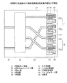
図13は、従来の導波路集積型光受信器の概念的平面図であり、同一の基板51上に入力導波路52、2×4MMI導波路53、PD接続導波路54及びフォトダイオード55を集積化している。そのため、各素子或いは導波路の間でレンズなどの光学部品が不要であるため、小型化や組立コストの観点から有望である。
FIG. 13 is a conceptual plan view of a conventional waveguide integrated optical receiver, in which an
図14は、従来のエバネッセント結合型の導波路集積型光受信器の構成説明図であり、ここでは、PD接続導波路及びフォトダイオードのみを示している。図14(a)は概念的斜視図であり、図14(b)は図14(a)におけるA面で切った概念的断面図であり、図14(c)は図14(a)におけるB面で切った概念的断面図である。 FIG. 14 is a diagram for explaining the configuration of a conventional evanescent coupling type waveguide integrated optical receiver. Here, only a PD connection waveguide and a photodiode are shown. 14 (a) is a conceptual perspective view, FIG. 14 (b) is a conceptual cross-sectional view taken along plane A in FIG. 14 (a), and FIG. 14 (c) is a view in B in FIG. 14 (a). It is a conceptual sectional view cut by a plane.
従来の導波路集積型光受信器は、導波路コア層61からなる導波路部分60と、導波路コア層61の一部領域上にn型スペーサ層62、吸収層63、p型上部クラッド層64及びp型コンタクト層65を堆積させたPD部66とを集積した構造となっている。
A conventional waveguide integrated optical receiver includes a
n型スペーサ層62は、導波路コア層61より屈折率が高い半導体からなり、吸収層63は、信号光を吸収するようにバンドギャップが調整された半導体層であり、一般的にはi型半導体層である。
The n-
図14(b)に示すように、導波路コア層61を伝播してきた光は、PD部66に光が入射してからある程度の距離伝播した後に、n型スペーサ層62から吸収層63に染み出していき、最終的には吸収層63で吸収される。
As shown in FIG. 14 (b), the light propagating through the
しかし、図14に示した構造では、n側電極を表面側からとるために、フォトダイオードの両脇にn型スペーサ層を一部残しておく必要があり、その結果、図14(c)に示すように、フォトダイオード部分では導波路コア層がスラブ状に残る形になる。 However, in the structure shown in FIG. 14, in order to take the n-side electrode from the surface side, it is necessary to leave a part of the n-type spacer layer on both sides of the photodiode. As a result, the structure shown in FIG. As shown, the waveguide core layer remains in a slab shape at the photodiode portion.
このような形状では、導波路部60からPD部66に入射してきた光を横方向に閉じ込める機構は、導波路コア層61の上部に形成されたn型スペーサ層62の一部および吸収層63からなるメサ形状によるものだけとなる。したがって、光閉じ込め効果が比較的弱くなるため、PD部66に入射した光が横方向に逃げてしまい、十分な吸収効果が得られないという問題がある。
In such a shape, a mechanism for confining light incident on the
十分な吸収効率を得るためには、メサの両脇のn型スペーサ層62の残し厚を薄くすることで、n型スペーサ層62の一部からなるメサ形状を深くし、PD部66に入射した光が横方向へ逃げにくくすることが有効である。
In order to obtain sufficient absorption efficiency, the remaining thickness of the n-
しかし、n型スペーサ層62の残し厚が薄くなることによりn型電極層としての抵抗が増加するため、高周波帯域が低減するという問題がある。このように、従来の導波路集積型光受信器では、吸収効率の向上と素子抵抗の低減の両立が困難であるという問題がある。
However, since the remaining thickness of the n-
したがって、本発明は、導波路集積型光受信器における吸収効率の向上と素子抵抗の低減を両立することを目的とする。 Accordingly, an object of the present invention is to achieve both improvement in absorption efficiency and reduction in element resistance in a waveguide integrated optical receiver.
開示する一観点からは、半導体基板と、前記半導体基板上に形成された少なくともメサ状部を有する導波路コア層からなる導波路部と、前記導波路コア層の延長部上に順次積層された第1導電型スペーサ層、吸収層及び前記第1導電型と反対の第2導電型上部クラッド層を少なくとも有するエバネッセント結合型のフォトダイオード部とを少なくとも有し、前記第1導電型スペーサ層の少なくとも一部がメサ状であり、前記第1導電型スペーサ層の屈折率より小さな屈折率の第1導電型半導体層が、前記吸収層と接することなく前記メサ状の第1導電型スペーサ層の側面と接していることを特徴とする半導体光集積回路装置が提供される。 From one aspect disclosed, a semiconductor substrate, a waveguide portion formed of a waveguide core layer having at least a mesa portion formed on the semiconductor substrate, and an extension portion of the waveguide core layer are sequentially stacked. At least an evanescent coupling type photodiode portion having at least a first conductivity type spacer layer, an absorption layer, and a second conductivity type upper cladding layer opposite to the first conductivity type, and at least one of the first conductivity type spacer layers A part of the first conductive type semiconductor layer having a mesa shape and a refractive index smaller than the refractive index of the first conductive type spacer layer is not in contact with the absorbing layer, and the side surface of the mesa type first conductive type spacer layer The semiconductor optical integrated circuit device is provided in contact with the semiconductor optical integrated circuit device.
また、開示する別の観点からは、半導体基板上に少なくとも導波路コア層、第1導電型スペーサ層、吸収層及び第1導電型と反対の第2導電型クラッド層を順次堆積する工程と、前記第2導電型クラッド層乃至第1導電型スペーサ層の一部を除去して導波路部を形成する工程と、第1のマスクを利用して前記導波路部における前記導波路コア層の少なくとも一部を除去してメサ状部を形成する工程と、前記導波路部以外の領域において、第2のマスクを利用して前記第2導電型クラッド層と吸収層と、前記第1導電型スペーサ層の少なくとも一部を除去してメサ状部を備えたエバネッセント結合型のフォトダイオード部を形成する工程と、前記第2のマスクを残存させた状態で、前記フォトダイオード部のメサ状部の両脇に露出する前記第1導電型スペーサ層上に、前記第1導電型スペーサ層の屈折率より小さな屈折率の第1導電型半導体層を前記吸収層の側面と接しないように形成する工程とを有することを特徴とする半導体光集積回路装置の製造方法が提供される。 According to another disclosed aspect, a step of sequentially depositing at least a waveguide core layer, a first conductivity type spacer layer, an absorption layer, and a second conductivity type cladding layer opposite to the first conductivity type on a semiconductor substrate; Removing a part of the second conductivity type cladding layer to the first conductivity type spacer layer to form a waveguide portion; and utilizing at least the waveguide core layer in the waveguide portion using a first mask A step of removing a part to form a mesa-like portion; and in a region other than the waveguide portion, the second conductive type cladding layer, the absorbing layer, and the first conductive type spacer using a second mask Removing at least a portion of the layer to form an evanescent coupled photodiode portion having a mesa-shaped portion, and both the mesa-shaped portions of the photodiode portion with the second mask remaining. The first exposed to the side The conductivity type spacer layer, characterized by a step of forming a first conductive type semiconductor layer of lower refractive index than the refractive index of the first conductivity type spacer layer so as not to contact with the side surface of the absorbent layer A method of manufacturing a semiconductor optical integrated circuit device is provided.
開示の半導体光集積回路装置及びその製造方法によれば、吸収効率の向上と素子抵抗の低減の両立が可能になる。 According to the disclosed semiconductor optical integrated circuit device and the manufacturing method thereof, it is possible to improve the absorption efficiency and reduce the element resistance.
ここで、図1を参照して、本発明の実施の形態の半導体光集積回路装置を説明する。図1は、本発明の実施の形態の半導体光集積回路装置の概念的構成図であり、図1(a)は斜視図であり、図1(b)が光軸に垂直な断面図である。図に示すように、半導体基板11上に形成された導波路部14とフォトダイオード部20とからなる。
Here, a semiconductor optical integrated circuit device according to an embodiment of the present invention will be described with reference to FIG. FIG. 1 is a conceptual configuration diagram of a semiconductor optical integrated circuit device according to an embodiment of the present invention, FIG. 1 (a) is a perspective view, and FIG. 1 (b) is a cross-sectional view perpendicular to the optical axis. . As shown in the figure, it comprises a
導波路部14は半導体基板11上に形成された少なくともメサ状部13を有する導波路コア層12からなる。この場合の導波路コア層12は全体が完全にメサ状であっても良い。また、メサ状部13の上にクラッド層を設けても良く、フォトダイオード部に入射した光が広がりやすいので、吸収層16における吸収効果を大きくすることができる。
The
フォトダイオード部20は、導波路コア層12の延長部上に順次積層された第1導電型スペーサ層15、吸収層16及び前記第1導電型と反対の第2導電型上部クラッド層17を少なくとも有する。また、第1導電型スペーサ層15の少なくとも一部がメサ状であり、メサ状の第1導電型スペーサ層15の側面が、第1導電型スペーサ層15の屈折率より小さな屈折率の第1導電型半導体層19と接している。なお、通常は第2導電型上部クラッド層17上に第2導電型コンタクト層18を設ける。
The
また、第1導電型スペーサ層15は完全にメサ状であっても良い。また、第1導電型半導体層19の上面は、第1導電型スペーサ層15の上面よりも下にあることが望ましく、それによって、吸収層16の側面においてリーク電流の経路をなくすことができる。
The first conductivity
また、このような半導体光集積回路装置を2×4MMI等の多モード干渉導波路等の他の光デバイスと集積化する場合には、導波路コア層12の入力端を多モード干渉導波路等の光デバイスとモノリシックに一体化すれば良い。
When such a semiconductor optical integrated circuit device is integrated with another optical device such as a multimode interference waveguide such as 2 × 4 MMI, the input end of the
本発明の実施の形態の半導体光集積回路装置では、フォトダイオード部においてストライプ状の第1導電型スペーサ層が屈折率の小さい第1導電型半導体層で挟まれた構造となっている。そのため、フォトダイオード部に入射してきた光の水平方向の広がりが抑制されるため、光が効率良く吸収層へ伝搬し高い受光感度が得られる。即ち、十分な吸収効率を維持したままフォトダイオード長を短くすることができる。 The semiconductor optical integrated circuit device according to the embodiment of the present invention has a structure in which a stripe-shaped first conductivity type spacer layer is sandwiched between first conductivity type semiconductor layers having a small refractive index in the photodiode portion. For this reason, since the spread of the light incident on the photodiode portion in the horizontal direction is suppressed, the light efficiently propagates to the absorption layer and high light receiving sensitivity is obtained. That is, the photodiode length can be shortened while maintaining sufficient absorption efficiency.
また、第1導電型半導体層のドーピング濃度や厚さを適切に設計することにより、第1導電型用の電極側の素子抵抗を低くすることができるため、高周波特性を改善することができる。したがって、フォトダイオード部の接合容量低減に有利な短いフォトダイオード長で、高い吸収効率と低い素子抵抗とを両立することが可能になる。 In addition, by appropriately designing the doping concentration and thickness of the first conductivity type semiconductor layer, the element resistance on the electrode side for the first conductivity type can be lowered, so that the high frequency characteristics can be improved. Therefore, it is possible to achieve both high absorption efficiency and low element resistance with a short photodiode length that is advantageous for reducing the junction capacitance of the photodiode portion.
以上を前提として、次に、図2乃至図5を参照して、本発明の実施例1の半導体光集積回路装置の製造工程を説明する。まず、図2(a)に示すように、有機金属気相成長法(MOVPE法)を用いて、(100)を主面とする半絶縁性InP基板21上に、厚さが0.5μmのi型InGaAsP導波路コア層22を堆積する。引き続いて、厚さが0.7μmのn型InGaAsPスペーサ層23、厚さが0.5μmのi型InGaAs吸収層24、厚さが1.0μmのp型InP上部クラッド層25及び厚さが0.3μmのp型InGaAsコンタクト層26を順次積層する。
Based on the above, the manufacturing process of the semiconductor optical integrated circuit device according to the first embodiment of the present invention will be described next with reference to FIGS. First, as shown in FIG. 2A, a thickness of 0.5 μm is formed on a
次いで、図2(b)に示すように、フォトダイオード形成部を除いて、p型InGaAsコンタクト層26乃至n型InGaAsPスペーサ層23をエッチング除去して導波路部27を形成する。次いで、図2(c)に示すように、SiO2マスク28を用いてi型InGaAsP導波路コア層22をエッチングしてリブ構造29を形成する。
Next, as shown in FIG. 2B, the
次いで、図3(d)に示すように、新たなSiO2マスク30を用いて、p型InGaAsコンタクト層26乃至n型InGaAsPスペーサ層23をストライプ状にエッチングして幅3μm、長さ25μmのフォトダイオード部31を形成する。
Next, as shown in FIG. 3D, the p-type
次いで、図3(e)に示すように、SiO2マスク30をそのまま残存させた状態で、有機金属気相成長法を用いて露出するn型InGaAsPスペーサ層23上にドーピング濃度が2×1018cm−3で厚さが0.6μmのn型InP層32を選択成長させる。この時、メサ状のフォトダイオード部31の側面で横方向に堆積するn型InP層32の厚さを薄くするために、メサ側面を(011)面とし、高温・低圧の成長条件で形成する。なお、n型InP層32を形成する際に、原料に塩素系原料を添加することで、横方向に堆積するn型InP層32の厚さをさらに薄くすることができる。
Next, as shown in FIG. 3E, the doping concentration is 2 × 10 18 on the n-type
次いで、図3(f)に示すように、エッチングにより、フォトダイオード部31のメサ側面で横方向に堆積したn型InP層32を除去する。エッチング量としては、例えば、0.1μmとする。この工程によりi型InGaAs吸収層24の側面においてリーク電流の経路がなくなるので、暗電流が抑制でき素子特性が向上する。
Next, as shown in FIG. 3F, the n-
以降は、SiO2マスク30を除去したのち、SiN等のパッシベーション膜(図4は省略)を形成したのち、コンタクト用開口部を形成し、p型InGaAsコンタクト層26上にAuZn/Auからなるp側電極33を形成する。一方、n型InP層32上にはAuGe/Auからなるn側電極34を形成することにより、半導体光集積回路装置の基本構成が完成する。
Thereafter, after removing the SiO 2 mask 30 and forming a passivation film such as SiN (not shown in FIG. 4), a contact opening is formed, and a p made of AuZn / Au is formed on the p-type
図4は、完成した本発明の実施例1の半導体光集積回路装置の説明図であり、図4(a)は、概略的斜視図であり、図4(b)は光軸に垂直な概略的断面図である。p側電極33とn側電極34の間に電圧を印加し、i型InGaAsP導波路コア層22を伝搬してきた光をi型InGaAs吸収層によって吸収し、発生したフォトキャリアをp側電極33及びn側電極34から引き出す。
4A and 4B are explanatory views of the completed semiconductor optical integrated circuit device according to the first embodiment of the present invention. FIG. 4A is a schematic perspective view, and FIG. 4B is a schematic view perpendicular to the optical axis. FIG. A voltage is applied between the p-
図4(c)は、本発明の実施例1の半導体光集積回路装置の効果の説明図であり、従来のn型InGaAsPスペーサ層を薄く残した場合のn側の素子抵抗の変化を示している。上述のように、光閉じ込め効果を高めるために、n型InGaAsPスペーサ層の残し膜厚を薄くするほどn側の素子抵抗が飛躍的に高くなっている。 FIG. 4C is an explanatory diagram of the effect of the semiconductor optical integrated circuit device according to the first embodiment of the present invention, and shows a change in element resistance on the n side when the conventional n-type InGaAsP spacer layer is left thin. Yes. As described above, in order to enhance the light confinement effect, the element resistance on the n side increases dramatically as the remaining film thickness of the n-type InGaAsP spacer layer is reduced.
一方、本発明の実施例1では、ストライプ状のInGaAsPスペーサ層が屈折率のより小さなn型InP層32で挟まれた構造となっている。そのため、フォトダイオード部に入射してきた光の水平方向の広がりを抑制しつつ、n型InP層32の厚さを0.5μmと設計することによりn側の素子抵抗を12.5Ωに低減することができる。
On the other hand, the first embodiment of the present invention has a structure in which a striped InGaAsP spacer layer is sandwiched between n-type InP layers 32 having a lower refractive index. Therefore, the element resistance on the n side is reduced to 12.5Ω by designing the thickness of the n-
図5は、本発明の実施例1の変形例であり、図5(a)はi型InGaAsP導波路コア層22をリブ構造ではなく完全なストライプ導波路構造にしたものである。また、図5(b)は、n型InGaAsPスペーサ層をメサの両脇において、光閉じ込め効果を損なわないように薄く残存させたものである。
FIG. 5 shows a modification of the first embodiment of the present invention. FIG. 5A shows the i-type InGaAsP
次に、図6乃至図8を参照して、本発明の実施例2の半導体光集積回路装置を説明する。まず、図6(a)に示すように、有機金属気相成長法(MOVPE法)を用いて、(100)を主面とする半絶縁性InP基板21上に、厚さが0.5μmのi型InGaAsP導波路コア層22を堆積する。引き続いて、厚さが0.7μmのn型InGaAsPスペーサ層23、厚さが0.5μmのi型InGaAs吸収層24、厚さが1.0μmのp型InP上部クラッド層25及び厚さが0.3μmのp型InGaAsコンタクト層26を順次積層する。
Next, a semiconductor optical integrated circuit device according to a second embodiment of the present invention will be described with reference to FIGS. First, as shown in FIG. 6A, a thickness of 0.5 μm is formed on a
次いで、図6(b)に示すように、フォトダイオード形成部を除いて、p型InGaAsコンタクト層26乃至n型InGaAsPスペーサ層23をエッチング除去して導波路部27を形成する。次いで、図3(c)に示すように、導波路部27において露出しているi型InGaAsP導波路コア層22上に厚さが1.7μmのi型InPクラッド層35を成長させる。
Next, as shown in FIG. 6B, the p-type
次いで、図7(d)に示すように、SiO2マスク36を用いてp型InGaAsコンタクト層26乃至n型InGaAsPスペーサ層23をストライプ状にエッチングして幅3μm、長さ25μmのフォトダイオード部31を形成する。この時、導波路部27においては、i型InPクラッド層35を半絶縁性InP基板21が0.3μm程度掘れるようにエッチングしてストライプ状メサを同時に形成する。
Next, as shown in FIG. 7D, the p-type
次いで、図7(e)に示すように、SiO2マスク36をそのまま残存させた状態で、導波路部27を覆うSiO2マスク37を形成する。次いで、有機金属気相成長法を用いて露出するn型InGaAsPスペーサ層23上にドーピング濃度が2×1018cm−3で厚さが0.6μmのn型InP層32を選択成長させる。この場合も、メサ状のフォトダイオード部31の側面で横方向に堆積するn型InP層32の厚さを薄くするために、メサ側面を(011)面とし、高温・低圧の成長条件で形成する。なお、n型InP層32を形成する際に、原料に塩素系原料を添加することで、横方向に堆積するn型InP層32の厚さをさらに薄くすることができる。
Next, as shown in FIG. 7E, a SiO 2 mask 37 covering the
次いで、図7(f)に示すように、エッチングにより、フォトダイオード部31のメサ側面で横方向に堆積したn型InP層32を除去する。エッチング量としては、例えば、0.1μmとする。この工程によりi型InGaAs吸収層24の側面においてリーク電流の経路がなくなるので、暗電流が抑制でき素子特性が向上する。
Next, as shown in FIG. 7F, the n-
以降は、SiO2マスク36,37を除去したのち、SiN等のパッシベーション膜(図4は省略)を形成したのち、コンタクト用開口部を形成し、p型InGaAsコンタクト層26上にAuZn/Auからなるp側電極33を形成する。一方、n型InP層32上にはAuGe/Auからなるn側電極34を形成することにより、本発明の実施例2の半導体光集積回路装置の基本構成が完成する。
Thereafter, after removing the SiO 2 masks 36 and 37, a passivation film such as SiN (not shown in FIG. 4) is formed, a contact opening is formed, and AuZn / Au is formed on the p-type
図8は、完成した本発明の実施例2の半導体光集積回路装置の説明図であり、図8(a)は、概略的斜視図であり、図8(b)及び図8(c)は本発明の効果の説明図である。図8(a)に示すように、導波路部の構造が異なるだけで、フォトダイオード部の構造は上記の実施例1と全く同じである。 FIG. 8 is an explanatory diagram of the completed semiconductor optical integrated circuit device according to the second embodiment of the present invention. FIG. 8A is a schematic perspective view, and FIG. 8B and FIG. It is explanatory drawing of the effect of this invention. As shown in FIG. 8A, the structure of the photodiode portion is exactly the same as that of the first embodiment, except that the structure of the waveguide portion is different.
図8(b)は、本発明の実施例2の吸収効率とのスペーサ膜厚依存性の説明図であり、ここでは、比較のために、n型InP層を設けずにn型InGaAsPスペーサ層を残存させた場合を比較している。本発明の実施例2では、ストライプ状のフォトダイオード部以外のn型スペーサ層を全て除去した構造で、且つ、ストライプ状のn型スペーサ層が屈折率の小さいn型InP層で挟まれた構造となっているため、高い吸収効率82%が得られる。また、n型InP層の厚さを0.5μmと設計することにより第1の実施例と同様にn側の素子抵抗を12.5Ωに低減することができる。 FIG. 8B is an explanatory diagram of the dependency of the spacer efficiency on the absorption efficiency of Example 2 of the present invention. Here, for comparison, an n-type InGaAsP spacer layer is provided without providing an n-type InP layer. Is compared. In Example 2 of the present invention, the n-type spacer layer other than the striped photodiode portion is completely removed, and the striped n-type spacer layer is sandwiched between n-type InP layers having a low refractive index. Therefore, a high absorption efficiency of 82% can be obtained. Further, by designing the thickness of the n-type InP layer to be 0.5 μm, the element resistance on the n side can be reduced to 12.5Ω as in the first embodiment.
図8(c)は、本発明の実施例2の吸収効率のフォトダイオード素子長依存性の説明図であり、ここでは比較構造として、n型InP層を設けずに、n型スペーサ層を0.5μmの厚さだけ残した構造を比較する。図に示すように、吸収効率80%に必要なフォトダイオード素子長を見ると、比較構造では34μmの長さが必要であることに対し、本発明の実施例2では23μmと短いフォトダイオード素子長まで短縮可能である。 FIG. 8C is an explanatory diagram of the dependency of the absorption efficiency on the photodiode element length according to the second embodiment of the present invention. Here, as a comparative structure, an n-type spacer layer is not provided without an n-type InP layer. Compare the structures left only 5 μm thick. As shown in the figure, when looking at the photodiode element length required for the absorption efficiency of 80%, the comparative structure requires a length of 34 μm, whereas in Example 2 of the present invention, the photodiode element length is as short as 23 μm. Can be shortened.
このことから、本発明の実施例2においては短いフォトダイオード素子長で高い受光感度が得られるためフォトダイオード素子のpin接合部の容量を小さくでき、十分な吸収効率を維持したまま高周波特性を確保すること可能となる。 Therefore, in Example 2 of the present invention, high light receiving sensitivity can be obtained with a short photodiode element length, so that the capacitance of the pin junction of the photodiode element can be reduced, and high frequency characteristics can be secured while maintaining sufficient absorption efficiency. It becomes possible to do.
このように、本発明の実施例2においては、実施例1と比較してフォトダイオード素子の吸収効率を大きくする効果がより顕著になり、特に、高周波帯域に有利なメサ幅の狭いフォトダイオード素子でより効果的である。 As described above, in the second embodiment of the present invention, the effect of increasing the absorption efficiency of the photodiode element is more remarkable than in the first embodiment, and in particular, a photodiode element having a narrow mesa width that is advantageous in a high frequency band. It is more effective.
次に、図9乃至図10を参照して、本発明の実施例3の半導体光集積回路装置を説明する。図9は本発明の実施例3の半導体光集積回路装置の説明図であり、図9(a)は概略的斜視図であり、図9(b)は光軸に沿った概略的断面図である。図に示すように、フォトダイオード部において、導波路コア層の下までメサ形状としている以外は、上記の実施例2と同様である。なお、このような構造を形成する際には、i型InPクラッド層35を厚く、例えば、2.5μm程度成膜して、同時にエッチングすれば良い。
Next, a semiconductor optical integrated circuit device according to a third embodiment of the present invention will be described with reference to FIGS. FIG. 9 is an explanatory diagram of a semiconductor optical integrated circuit device according to a third embodiment of the present invention, FIG. 9A is a schematic perspective view, and FIG. 9B is a schematic cross-sectional view along the optical axis. is there. As shown in the figure, the photodiode portion is the same as that of the second embodiment except that the mesa shape is formed below the waveguide core layer. When forming such a structure, the i-type
本発明の実施例3においては、メサの両脇を深くエッチング除去しているので、n型InP層を厚く形成しても、i型InGaAs吸収層の両側に暗電流のリークパスが形成されないので、素子抵抗をより低減することができる。 In Example 3 of the present invention, since both sides of the mesa are deeply etched away, even if the n-type InP layer is formed thick, no dark current leak path is formed on both sides of the i-type InGaAs absorption layer. The element resistance can be further reduced.
図10は、本発明の実施例3の効果の説明図であり、図10(a)に示すように、n側の素子抵抗は、n型InP層の膜厚の増大に伴って低減し、素子抵抗の低減によって、高周波帯域が改善される。 FIG. 10 is an explanatory diagram of the effect of Example 3 of the present invention. As shown in FIG. 10A, the n-side element resistance decreases as the film thickness of the n-type InP layer increases. The high frequency band is improved by reducing the element resistance.
図10(b)は、吸収効率の導波路コア層残し膜厚依存性の説明図である。フォトダイオード部の導波路コア層も完全にストライプ状となっているため、フォトダイオード部に入射してきた光の水平方向の広がりがさらに抑制されるため、吸収層の受光感度が改善する効果も得られる。 FIG. 10B is an explanatory diagram of the dependency of the absorption efficiency on the remaining thickness of the waveguide core layer. Since the waveguide core layer of the photodiode part is also completely striped, the horizontal spread of the light incident on the photodiode part is further suppressed, and the light receiving sensitivity of the absorption layer is also improved. It is done.
次に、図11及び図12を参照して本発明の実施例4の半導体光集積回路装置を説明する。図11は、本発明の実施例4の半導体光集積回路装置の概念的平面図であり、図12は、本発明の実施例4の半導体光集積回路装置のフォトダイオード部の概略的斜視図である。図11に示すように、本発明の実施例4の半導体光集積回路装置は、QPSK(QuadraturePhase Shift Keying)変調方式の復調用の光コヒーレントレシーバ素子に適用した例である。 Next, a semiconductor optical integrated circuit device according to a fourth embodiment of the present invention will be described with reference to FIGS. FIG. 11 is a conceptual plan view of the semiconductor optical integrated circuit device according to the fourth embodiment of the present invention. FIG. 12 is a schematic perspective view of the photodiode portion of the semiconductor optical integrated circuit device according to the fourth embodiment of the present invention. is there. As shown in FIG. 11, the semiconductor optical integrated circuit device according to the fourth embodiment of the present invention is an example applied to a demodulating optical coherent receiver element of a QPSK (Quadrature Phase Shift Keying) modulation method.
この場合、入力導波路部41、4×4MMI導波路42及びPD接続導波路43における積層構造は上記の実施例2の導波路部の積層構造と同じであり、フォトダイオード部44も実施例2のフォトダイオード部と同じである。なお、ここでは、入力導波路を2本として4×4MMI導波路42を実効的に2×4MMIとして使用する。
In this case, the laminated structure in the
ここで、簡単に製造工程を説明するが、基本的には上記の実施例2と同様であるので図示は省略するが、引用する符号は図12の符号を用いる。まず、有機金属気相成長法を用いて、(100)を主面とする半絶縁性InP基板21上に、厚さが0.5μmのi型InGaAsP導波路コア層22を堆積する。引き続いて、厚さが0.7μmのn型InGaAsPスペーサ層23、厚さが0.5μmのi型InGaAs吸収層24、厚さが1.0μmのp型InP上部クラッド層25及び厚さが0.3μmのp型InGaAsコンタクト層26を順次積層する。
Here, the manufacturing process will be briefly described, but since it is basically the same as that of the second embodiment, the illustration is omitted, but the reference numeral of FIG. 12 is used. First, an i-type InGaAsP
次いで、フォトダイオード形成部を除いて、p型InGaAsコンタクト層26乃至n型InGaAsPスペーサ層23をエッチング除去して導波路部27を形成する。次いで、導波路部27において露出しているi型InGaAsP導波路コア層22上に厚さが1.7μmのi型InPクラッド層35を成長させる。
Next, except for the photodiode forming portion, the p-type
次いで、SiO2マスクを用いてp型InGaAsコンタクト層26乃至n型InGaAsPスペーサ層23をストライプ状にエッチングして幅3μm、長さ25μmのフォトダイオード部44を形成する。この時、導波路部27においては、i型InPクラッド層35を半絶縁性InP基板21が0.3μm程度掘れるようにメサ状にエッチングして2本の入力導波路と、4×4MMI導波路と4本の接続導波路が形成する。
Next, the p-type
次いで、SiO2マスクをそのまま残存させた状態で、導波路部27を覆うSiO2マスクを形成する。次いで、有機金属気相成長法を用いて露出するn型InGaAsPスペーサ層23上にドーピング濃度が2×1018cm−3で厚さが0.6μmのn型InP層32を選択成長させる。この場合も、メサ状のフォトダイオード部44の側面で横方向に堆積するn型InP層32の厚さを薄くするために、メサ側面を(011)面とし、高温・低圧の成長条件で形成する。なお、n型InP層32を形成する際に、原料に塩素系原料を添加することで、横方向に堆積するn型InP層32の厚さをさらに薄くすることができる。
Next, a SiO 2 mask that covers the
次いで、エッチングにより、フォトダイオード部44のメサ側面で横方向に堆積したn型InP層32を除去する。エッチング量としては、例えば、0.1μmとする。この工程によりi型InGaAs吸収層24の側面においてリーク電流の経路がなくなるので、暗電流が抑制でき素子特性が向上する。
Next, the n-
次いで、隣接するフォトダイオード間のn型InP層32を選択的に除去して分離溝45を形成する。以降は、マスクを除去したのち、SiN等のパッシベーション膜(図4は省略)を形成したのち、コンタクト用開口部を形成し、p型InGaAsコンタクト層26上にAuZn/Auからなるp側電極33を形成する。一方、n型InP層32上にはAuGe/Auからなるn側電極34を形成することにより、図11及び図12に示す本発明の実施例4の半導体光集積回路装置の基本構成が完成する。
Next, the n-
図11に示すように、2本の入力導波路41の内の1本は、ハイブリッド導波路となる4×4MMI導波路42の図で上から2番目に接続されており、他の1本は、上から4番目に接続されている。フォトダイオード部44は、4個のフォトダイオードPD1、PD2、PD3、PD4からなる。
As shown in FIG. 11, one of the two
4×4MMI導波路42の4個の出力を上から1,2,3,4とした場合、PD1と出力1、PD2と出力4、PD3と出力2、PD4と出力3がPD接続導波路43によって接続されている。また、各フォトダイオードには、メサの直上に信号電極となるp側電極が、n型InP層の表面上にはグランド電極となるn側電極が形成されている。
When the four outputs of the 4 × 4
このような構成において、上側の入力導波路にQPSKの変調信号光を、下側の入力導波路にローカルオシレータ(LO)光を入射することによって、QPSK変調方式のいわゆるIチャネル信号をPD1、PD2から、Qチャネル信号をPD3、PD4から取り出すことができる。このような構成においても、上記の実施例2の素子構造を採用することによって、高出力、広帯域動作が可能となる。なお、上記の実施例3の構造を採用しても良い。 In such a configuration, a QPSK modulation signal light is incident on the upper input waveguide, and a local oscillator (LO) light is incident on the lower input waveguide, whereby a so-called I channel signal of the QPSK modulation method is converted into PD 1 , From PD 2 , the Q channel signal can be extracted from PD 3 and PD 4 . Even in such a configuration, by adopting the element structure of the second embodiment, high output and wide band operation can be performed. In addition, you may employ | adopt the structure of said Example 3. FIG.
図12は、フォトダイオード部の概略的斜視図であり、4個のフォトダイオードの間で電気的な分離を十分に取るために、分離溝45を形成してn型InP層32が独立して存在した構造としている。なお、図面の簡略のために、2個のフォトダイオード部のみを示し、また、電極は省略している。
FIG. 12 is a schematic perspective view of the photodiode portion. In order to sufficiently separate the four photodiodes, the n-
なお、上記の各実施例では、InGaAsP系の材料で構成したフォトダイオードの例を述べているが、これに限らず適宜、吸収層は入射光の波長帯の光を吸収し、その他の層は入射光を吸収しないような材料系で形成した光受信器においても本発明の構造を適用することができる。 In each of the above-described embodiments, an example of a photodiode composed of an InGaAsP-based material is described. However, the present invention is not limited to this, and the absorption layer absorbs light in the wavelength band of incident light as appropriate. The structure of the present invention can also be applied to an optical receiver formed of a material system that does not absorb incident light.
また、吸収層などはi型半導体の例を示しているが、例えば吸収層の一部、あるいは、全てがp型あるいはn型の半導体であっても良い。また、上記の各実施例ではフォトダイオード部の導波路構造としてハイメサ構造の場合を示しているが、一部または、全てが埋め込み型導波路になっているような構造でも、本発明の効果を同様に得ることができる。 In addition, although an example of an i-type semiconductor is shown as the absorption layer, for example, a part or all of the absorption layer may be a p-type or n-type semiconductor. In each of the above embodiments, the high mesa structure is shown as the waveguide structure of the photodiode portion. However, the effects of the present invention can be achieved even in a structure in which a part or all of the waveguide structure is a buried waveguide. It can be obtained similarly.
また、上記の各実施例では、導波路集積型の光受信器として光コヒーレントレシーバに関して記載しているが、これに限らず、フォトダイオードと導波路が集積されている各種の半導体光集積回路装置に適用されるものである。 In each of the above embodiments, an optical coherent receiver is described as a waveguide integrated optical receiver. However, the present invention is not limited to this, and various semiconductor optical integrated circuit devices in which a photodiode and a waveguide are integrated are described. Applies to
ここで、実施例1乃至実施例4を含む本発明の実施の形態に関して、以下の付記を付す。
(付記1)半導体基板と、前記半導体基板上に形成された少なくともメサ状部を有する導波路コア層からなる導波路部と、前記導波路コア層の延長部上に順次積層された第1導電型スペーサ層、吸収層及び前記第1導電型と反対の第2導電型上部クラッド層を少なくとも有するエバネッセント結合型のフォトダイオード部とを少なくとも有し、前記第1導電型スペーサ層の少なくとも一部がメサ状であり、前記第1導電型スペーサ層の屈折率より小さな屈折率の第1導電型半導体層が、前記吸収層と接することなく前記メサ状の第1導電型スペーサ層の側面と接していることを特徴とする半導体光集積回路装置。
(付記2)前記第1導電型半導体層の上面が、前記第1導電型スペーサ層の上面よりも下にあることを特徴とする付記1に記載の半導体光集積回路装置。
(付記3)前記第1導電型スペーサ層が完全にメサ状であるとともに、前記フォトダイオード部における前記導波路コア層の少なくとも一部がメサ状であり、前記メサ状の導波路コア層と第1導電型スペーサ層の側面が、前記第1導電型半導体層と接していることを特徴とする付記1または付記2に記載の半導体光集積回路装置。
(付記4)前記第2導電型クラッド層上に、直接或いはコンタクト用半導体層を介して第2導電型用の電極を有するとともに、前記第1導電型半導体層の表面に第1導電型用の電極を有することを特徴とする付記1乃至付記3のいずれか1に記載の半導体光集積回路装置。
(付記5)前記導波路部における導波路コア層の上にメサストライプ状のクラッド層を有することを特徴とする付記1乃至付記4のいずれか1に記載の半導体光集積回路装置。
(付記6)前記導波路部における導波路コア層がメサストライプ構造であり、前記導波路コア層の入力端が多モード干渉導波路とモノリシックに結合していることを特徴とする付記1乃至付記5のいずれか1に記載の半導体光集積回路装置。
(付記7)半導体基板上に少なくとも導波路コア層、第1導電型スペーサ層、吸収層及び前記第1導電型と反対の第2導電型クラッド層を順次堆積する工程と、前記第2導電型クラッド層乃至第1導電型スペーサ層の一部を除去して導波路部を形成する工程と、第1のマスクを利用して前記導波路部における前記導波路コア層の少なくとも一部を除去してメサ状部を形成する工程と、前記導波路部以外の領域において、第2のマスクを利用して前記第2導電型クラッド層と吸収層と、前記第1導電型スペーサ層の少なくとも一部を除去してメサ状部を備えたエバネッセント結合型のフォトダイオード部を形成する工程と、前記第2のマスクを残存させた状態で、前記フォトダイオード部のメサ状部の両脇に露出する前記第1導電型スペーサ層上に、第1導電型スペーサ層の屈折率より小さな屈折率の第1導電型半導体層を前記吸収層の側面と接しないように形成する工程とを有することを特徴とする半導体光集積回路装置の製造方法。
(付記8)前記フォトダイオード部のメサ状部の側面に横方向に堆積した第1導電型半導体層を除去する工程を有することを特徴とする付記7に記載の半導体光集積回路装置の製造方法。
(付記9)前記導波路部を形成したのち、前記導波路部における導波路コア層上にクラッド層を形成する工程を有し、前記第1のマスクを利用して前記導波路部における前記導波路コア層の少なくとも一部を除去してメサ状部を形成する工程と、前記導波路部以外の領域において、第2のマスクを利用して前記第2導電型クラッド層と吸収層と、前記第1導電型スペーサ層の少なくとも一部を除去してメサ状部を備えたフォトダイオード部を形成する工程とが同時に行う単一のエッチング工程であることを特徴とする付記7または付記8に記載の半導体光集積回路装置の製造方法。
Here, the following supplementary notes are attached to the embodiments of the present invention including Examples 1 to 4.
(Additional remark 1) The 1st electroconductivity laminated | stacked sequentially on the semiconductor substrate, the waveguide part which consists of a waveguide core layer which has at least mesa-like part formed on the said semiconductor substrate, and the extension part of the said waveguide core layer At least a part of the first conductivity type spacer layer, wherein the at least part of the first conductivity type spacer layer includes a type spacer layer, an absorption layer, and an evanescent coupling type photodiode portion having at least a second conductivity type upper cladding layer opposite to the first conductivity type. A first conductive semiconductor layer that is mesa-shaped and has a refractive index smaller than the refractive index of the first conductive spacer layer is in contact with the side surface of the mesa-shaped first conductive spacer layer without being in contact with the absorbing layer. the semiconductor optical integrated circuit device characterized by there.
(Supplementary note 2) The semiconductor optical integrated circuit device according to
(Supplementary Note 3) The first conductivity type spacer layer is completely mesa-shaped, and at least a part of the waveguide core layer in the photodiode portion is mesa-shaped, and the mesa-shaped waveguide core layer and the first 3. The semiconductor optical integrated circuit device according to
(Supplementary Note 4) An electrode for the second conductivity type is provided on the second conductivity type cladding layer directly or via a contact semiconductor layer, and the first conductivity type semiconductor layer is provided on the surface of the first conductivity type semiconductor layer. 4. The semiconductor optical integrated circuit device according to any one of
(Supplementary note 5) The semiconductor optical integrated circuit device according to any one of
(Supplementary note 6) The
(Appendix 7) A step of sequentially depositing at least a waveguide core layer, a first conductivity type spacer layer, an absorption layer, and a second conductivity type cladding layer opposite to the first conductivity type on a semiconductor substrate, and the second conductivity type Removing a portion of the cladding layer to the first conductivity type spacer layer to form a waveguide portion; and removing at least a portion of the waveguide core layer in the waveguide portion using a first mask. Forming a mesa-shaped portion, and in a region other than the waveguide portion, using the second mask, the second conductive type cladding layer, the absorbing layer, and at least a part of the first conductive type spacer layer Forming an evanescent coupling type photodiode portion having a mesa-shaped portion, and exposing the both sides of the mesa-shaped portion of the photodiode portion with the second mask remaining. First conductivity type spacer layer To, semiconductor optical integrated circuit apparatus characterized by a step of forming a first conductive type semiconductor layer of lower refractive index than the refractive index of the first conductive type spacer layer so as not to contact with the side surface of the absorbent layer Production method.
(Supplementary note 8) The method of manufacturing a semiconductor optical integrated circuit device according to supplementary note 7, comprising a step of removing the first conductive semiconductor layer deposited laterally on the side surface of the mesa-shaped portion of the photodiode portion. .
(Supplementary note 9) A step of forming a cladding layer on a waveguide core layer in the waveguide portion after forming the waveguide portion, and using the first mask to conduct the guiding in the waveguide portion. Removing at least a portion of the waveguide core layer to form a mesa-shaped portion; and in a region other than the waveguide portion, using the second mask, the second conductivity type cladding layer and the absorption layer; Appendix 7 or
11 半導体基板
12 導波路コア層
13 メサ状部
14 導波路部
15 第1導電型スペーサ層
16 吸収層
17 第2導電型上部クラッド層
18 第2導電型コンタクト層
19 第1導電型半導体層
20 フォトダイオード部
21 半絶縁性InP基板
22 i型InGaAsP導波路コア層
23 n型InGaAsPスペーサ層
24 i型InGaAs吸収層
25 p型InP上部クラッド層
26 p型InGaAsコンタクト層
27 導波路部
28 SiO2マスク
29 リブ構造
30 SiO2マスク
31 フォトダイオード部
32 n型InP層
33 p側電極
34 n側電極
35 i型InPクラッド層
36 SiO2マスク
37 SiO2マスク
41 入力導波路
42 4×4MMI導波路
43 PD接続導波路
44 フォトダイオード部
45 分離溝
51 基板
52 入力導波路
53 2×4MMI導波路
54 PD接続導波路
55 フォトダイオード
60 導波路部分
61 導波路コア層
62 n型スペーサ層
63 吸収層
64 p型上部クラッド層
65 p型コンタクト層
66 PD部
DESCRIPTION OF
Claims (5)
前記半導体基板上に形成された少なくともメサ状部を有する導波路コア層からなる導波路部と、
前記導波路コア層の延長部上に順次積層された第1導電型スペーサ層、吸収層及び前記第1導電型と反対の第2導電型上部クラッド層を少なくとも有するエバネッセント結合型のフォトダイオード部と
を少なくとも有し、
前記第1導電型スペーサ層の少なくとも一部がメサ状であり、
前記第1導電型スペーサ層の屈折率より小さな屈折率の第1導電型半導体層が、前記吸収層と接することなく前記メサ状の第1導電型スペーサ層の側面と接していることを特徴とする半導体光集積回路装置。 A semiconductor substrate;
A waveguide portion formed of a waveguide core layer having at least a mesa portion formed on the semiconductor substrate;
An evanescently coupled photodiode portion having at least a first conductivity type spacer layer, an absorption layer, and a second conductivity type upper clad layer opposite to the first conductivity type, which are sequentially stacked on an extension of the waveguide core layer; Having at least
At least a portion of the first conductivity type spacer layer is mesa-shaped;
The first conductivity type semiconductor layer having a refractive index smaller than the refractive index of the first conductivity type spacer layer is in contact with the side surface of the mesa-shaped first conductivity type spacer layer without being in contact with the absorption layer. A semiconductor optical integrated circuit device.
前記メサ状の導波路コア層と第1導電型スペーサ層の側面が、前記第1導電型半導体層と接していることを特徴とする請求項1に記載の半導体光集積回路装置。 The first conductivity type spacer layer is completely mesa-shaped, and at least a part of the waveguide core layer in the photodiode portion is mesa-shaped,
2. The semiconductor optical integrated circuit device according to claim 1, wherein side surfaces of the mesa-shaped waveguide core layer and the first conductivity type spacer layer are in contact with the first conductivity type semiconductor layer.
前記導波路コア層の入力端が多モード干渉導波路とモノリシックに結合していることを特徴とする請求項1乃至請求項3のいずれか1項に記載の半導体光集積回路装置。 The waveguide core layer in the waveguide section has a mesa stripe structure,
4. The semiconductor optical integrated circuit device according to claim 1, wherein an input end of the waveguide core layer is monolithically coupled to a multimode interference waveguide. 5.
前記第2導電型クラッド層乃至第1導電型スペーサ層の一部を除去して導波路部を形成する工程と、
第1のマスクを利用して前記導波路部における前記導波路コア層の少なくとも一部を除去してメサ状部を形成する工程と、
前記導波路部以外の領域において、第2のマスクを利用して前記第2導電型クラッド層と吸収層と、前記第1導電型スペーサ層の少なくとも一部を除去してメサ状部を備えたエバネッセント結合型のフォトダイオード部を形成する工程と、
前記第2のマスクを残存させた状態で、前記フォトダイオード部のメサ状部の両脇に露出する前記第1導電型スペーサ層上に、前記第1導電型スペーサ層の屈折率より小さな屈折率の第1導電型半導体層を前記吸収層の側面と接しないように形成する工程と
を有することを特徴とする半導体光集積回路装置の製造方法。 Sequentially depositing at least a waveguide core layer, a first conductivity type spacer layer, an absorption layer, and a second conductivity type cladding layer opposite to the first conductivity type on a semiconductor substrate;
Removing a part of the second conductivity type cladding layer to the first conductivity type spacer layer to form a waveguide portion;
Removing at least a portion of the waveguide core layer in the waveguide portion using a first mask to form a mesa-like portion;
In a region other than the waveguide portion, a mesa-like portion is provided by removing at least a part of the second conductivity type cladding layer, the absorption layer, and the first conductivity type spacer layer using a second mask. Forming an evanescent coupled photodiode portion;
A refractive index smaller than the refractive index of the first conductivity type spacer layer on the first conductivity type spacer layer exposed on both sides of the mesa-like portion of the photodiode portion with the second mask remaining. And a step of forming the first conductivity type semiconductor layer so as not to contact the side surface of the absorption layer .
Priority Applications (1)
| Application Number | Priority Date | Filing Date | Title |
|---|---|---|---|
| JP2011051019A JP5655643B2 (en) | 2011-03-09 | 2011-03-09 | Semiconductor optical integrated circuit device and manufacturing method thereof |
Applications Claiming Priority (1)
| Application Number | Priority Date | Filing Date | Title |
|---|---|---|---|
| JP2011051019A JP5655643B2 (en) | 2011-03-09 | 2011-03-09 | Semiconductor optical integrated circuit device and manufacturing method thereof |
Publications (2)
| Publication Number | Publication Date |
|---|---|
| JP2012190875A JP2012190875A (en) | 2012-10-04 |
| JP5655643B2 true JP5655643B2 (en) | 2015-01-21 |
Family
ID=47083755
Family Applications (1)
| Application Number | Title | Priority Date | Filing Date |
|---|---|---|---|
| JP2011051019A Active JP5655643B2 (en) | 2011-03-09 | 2011-03-09 | Semiconductor optical integrated circuit device and manufacturing method thereof |
Country Status (1)
| Country | Link |
|---|---|
| JP (1) | JP5655643B2 (en) |
Families Citing this family (3)
| Publication number | Priority date | Publication date | Assignee | Title |
|---|---|---|---|---|
| JP6051792B2 (en) * | 2012-11-06 | 2016-12-27 | 住友電気工業株式会社 | Coherent mixer |
| JP6538969B2 (en) * | 2016-04-19 | 2019-07-03 | 日本電信電話株式会社 | Optical waveguide integrated light receiving element and method of manufacturing the same |
| KR102377319B1 (en) * | 2016-11-16 | 2022-03-24 | 한국전자통신연구원 | Photodetector device |
Family Cites Families (6)
| Publication number | Priority date | Publication date | Assignee | Title |
|---|---|---|---|---|
| JPH04286168A (en) * | 1991-03-14 | 1992-10-12 | Fujitsu Ltd | Avalanche photo-diode |
| JPH09153638A (en) * | 1995-11-30 | 1997-06-10 | Nec Corp | Waveguide semiconductor light receiving device and manufacture of the same |
| JP4291085B2 (en) * | 2003-08-25 | 2009-07-08 | 三菱電機株式会社 | Waveguide type light receiving element |
| JP2006066488A (en) * | 2004-08-25 | 2006-03-09 | Mitsubishi Electric Corp | Semiconductor light receiving element and manufacturing method thereof |
| JP4719763B2 (en) * | 2008-03-28 | 2011-07-06 | 日本オプネクスト株式会社 | Manufacturing method of receiver |
| JP5526611B2 (en) * | 2009-06-09 | 2014-06-18 | 日本電気株式会社 | Semiconductor light receiving element and method for manufacturing semiconductor light receiving element |
-
2011
- 2011-03-09 JP JP2011051019A patent/JP5655643B2/en active Active
Also Published As
| Publication number | Publication date |
|---|---|
| JP2012190875A (en) | 2012-10-04 |
Similar Documents
| Publication | Publication Date | Title |
|---|---|---|
| JP5742345B2 (en) | Light receiving element and light receiving module | |
| JP5897414B2 (en) | Optical device manufacturing method | |
| JP2982619B2 (en) | Semiconductor optical waveguide integrated photodetector | |
| US8724938B2 (en) | Optical receiver | |
| JP5742344B2 (en) | Light receiving element, optical receiver and optical receiving module | |
| JPH09153638A (en) | Waveguide semiconductor light receiving device and manufacture of the same | |
| US9122003B2 (en) | Semiconductor optical device | |
| JP6961621B2 (en) | Optical integrated device and optical transmitter module | |
| JP4762834B2 (en) | Optical integrated circuit | |
| JP2001091913A (en) | Modulator and semiconductor laser device with modulator and method for manufacturing the same | |
| JP5655643B2 (en) | Semiconductor optical integrated circuit device and manufacturing method thereof | |
| JP2015162576A (en) | Semiconductor optical integrated element and semiconductor optical integrated element manufacturing method | |
| JP5526611B2 (en) | Semiconductor light receiving element and method for manufacturing semiconductor light receiving element | |
| US7919349B2 (en) | Photonic integration scheme | |
| JP6205826B2 (en) | Semiconductor optical device manufacturing method | |
| JP2012248649A (en) | Semiconductor element and method for manufacturing semiconductor element | |
| JP6726248B2 (en) | Semiconductor light receiving element and photoelectric fusion module | |
| JPH06268196A (en) | Optical integrated device | |
| JP6213222B2 (en) | Optical semiconductor device and manufacturing method thereof | |
| JP5906973B2 (en) | Optical branching device and optical semiconductor integrated circuit device | |
| JP2671843B2 (en) | Semiconductor optical integrated device and manufacturing method thereof | |
| KR100265858B1 (en) | Wavelength division multiplexing device with monolithically integrated semiconductor laser and photodiode | |
| JPH11103088A (en) | Semiconductor waveguide light receiving element | |
| JP5906593B2 (en) | Manufacturing method of optical semiconductor integrated device | |
| JPH10256589A (en) | Waveguide type semiconductor photodetector and manufacture thereof |
Legal Events
| Date | Code | Title | Description |
|---|---|---|---|
| A621 | Written request for application examination |
Free format text: JAPANESE INTERMEDIATE CODE: A621 Effective date: 20131129 |
|
| A977 | Report on retrieval |
Free format text: JAPANESE INTERMEDIATE CODE: A971007 Effective date: 20140326 |
|
| A131 | Notification of reasons for refusal |
Free format text: JAPANESE INTERMEDIATE CODE: A131 Effective date: 20140408 |
|
| A521 | Request for written amendment filed |
Free format text: JAPANESE INTERMEDIATE CODE: A523 Effective date: 20140514 |
|
| A131 | Notification of reasons for refusal |
Free format text: JAPANESE INTERMEDIATE CODE: A131 Effective date: 20140729 |
|
| A521 | Request for written amendment filed |
Free format text: JAPANESE INTERMEDIATE CODE: A523 Effective date: 20140908 |
|
| TRDD | Decision of grant or rejection written | ||
| A01 | Written decision to grant a patent or to grant a registration (utility model) |
Free format text: JAPANESE INTERMEDIATE CODE: A01 Effective date: 20141028 |
|
| A61 | First payment of annual fees (during grant procedure) |
Free format text: JAPANESE INTERMEDIATE CODE: A61 Effective date: 20141110 |
|
| R150 | Certificate of patent or registration of utility model |
Ref document number: 5655643 Country of ref document: JP Free format text: JAPANESE INTERMEDIATE CODE: R150 |