JP5654588B2 - Electrode and manufacturing method thereof - Google Patents
Electrode and manufacturing method thereof Download PDFInfo
- Publication number
- JP5654588B2 JP5654588B2 JP2012517905A JP2012517905A JP5654588B2 JP 5654588 B2 JP5654588 B2 JP 5654588B2 JP 2012517905 A JP2012517905 A JP 2012517905A JP 2012517905 A JP2012517905 A JP 2012517905A JP 5654588 B2 JP5654588 B2 JP 5654588B2
- Authority
- JP
- Japan
- Prior art keywords
- electrode
- photosensitive paste
- boron
- weight
- powder
- Prior art date
- Legal status (The legal status is an assumption and is not a legal conclusion. Google has not performed a legal analysis and makes no representation as to the accuracy of the status listed.)
- Active
Links
- 238000004519 manufacturing process Methods 0.000 title claims description 14
- ZOXJGFHDIHLPTG-UHFFFAOYSA-N Boron Chemical compound [B] ZOXJGFHDIHLPTG-UHFFFAOYSA-N 0.000 claims description 63
- RYGMFSIKBFXOCR-UHFFFAOYSA-N Copper Chemical compound [Cu] RYGMFSIKBFXOCR-UHFFFAOYSA-N 0.000 claims description 58
- 239000011521 glass Substances 0.000 claims description 32
- 239000002245 particle Substances 0.000 claims description 26
- 239000000178 monomer Substances 0.000 claims description 24
- 238000010304 firing Methods 0.000 claims description 19
- 238000000034 method Methods 0.000 claims description 17
- 239000003999 initiator Substances 0.000 claims description 13
- 238000001035 drying Methods 0.000 claims description 4
- 229910052796 boron Inorganic materials 0.000 description 29
- NIXOWILDQLNWCW-UHFFFAOYSA-M Acrylate Chemical compound [O-]C(=O)C=C NIXOWILDQLNWCW-UHFFFAOYSA-M 0.000 description 21
- 239000010949 copper Substances 0.000 description 21
- 229910052802 copper Inorganic materials 0.000 description 18
- 239000000203 mixture Substances 0.000 description 18
- 239000002491 polymer binding agent Substances 0.000 description 12
- 239000000758 substrate Substances 0.000 description 12
- 239000003960 organic solvent Substances 0.000 description 11
- 239000000470 constituent Substances 0.000 description 10
- 238000011161 development Methods 0.000 description 10
- 230000018109 developmental process Effects 0.000 description 10
- 230000003647 oxidation Effects 0.000 description 10
- 238000007254 oxidation reaction Methods 0.000 description 10
- 239000000523 sample Substances 0.000 description 10
- 229920000620 organic polymer Polymers 0.000 description 9
- 238000005245 sintering Methods 0.000 description 9
- 239000002904 solvent Substances 0.000 description 9
- BQCADISMDOOEFD-UHFFFAOYSA-N Silver Chemical compound [Ag] BQCADISMDOOEFD-UHFFFAOYSA-N 0.000 description 7
- 230000008569 process Effects 0.000 description 7
- 229910052709 silver Inorganic materials 0.000 description 7
- 239000004332 silver Substances 0.000 description 7
- LYCAIKOWRPUZTN-UHFFFAOYSA-N Ethylene glycol Chemical compound OCCO LYCAIKOWRPUZTN-UHFFFAOYSA-N 0.000 description 6
- PEDCQBHIVMGVHV-UHFFFAOYSA-N Glycerine Chemical compound OCC(O)CO PEDCQBHIVMGVHV-UHFFFAOYSA-N 0.000 description 6
- 238000000576 coating method Methods 0.000 description 6
- 239000000843 powder Substances 0.000 description 6
- 239000012298 atmosphere Substances 0.000 description 5
- 239000011230 binding agent Substances 0.000 description 5
- 239000011248 coating agent Substances 0.000 description 5
- 150000001875 compounds Chemical class 0.000 description 5
- 229910000510 noble metal Inorganic materials 0.000 description 5
- DAFHKNAQFPVRKR-UHFFFAOYSA-N (3-hydroxy-2,2,4-trimethylpentyl) 2-methylpropanoate Chemical compound CC(C)C(O)C(C)(C)COC(=O)C(C)C DAFHKNAQFPVRKR-UHFFFAOYSA-N 0.000 description 4
- RTZKZFJDLAIYFH-UHFFFAOYSA-N Diethyl ether Chemical compound CCOCC RTZKZFJDLAIYFH-UHFFFAOYSA-N 0.000 description 4
- OFOBLEOULBTSOW-UHFFFAOYSA-N Malonic acid Chemical compound OC(=O)CC(O)=O OFOBLEOULBTSOW-UHFFFAOYSA-N 0.000 description 4
- -1 N, N-dimethylaminoethyl Chemical group 0.000 description 4
- KDLHZDBZIXYQEI-UHFFFAOYSA-N Palladium Chemical compound [Pd] KDLHZDBZIXYQEI-UHFFFAOYSA-N 0.000 description 4
- CDBYLPFSWZWCQE-UHFFFAOYSA-L Sodium Carbonate Chemical compound [Na+].[Na+].[O-]C([O-])=O CDBYLPFSWZWCQE-UHFFFAOYSA-L 0.000 description 4
- 239000012670 alkaline solution Substances 0.000 description 4
- IISBACLAFKSPIT-UHFFFAOYSA-N bisphenol A Chemical compound C=1C=C(O)C=CC=1C(C)(C)C1=CC=C(O)C=C1 IISBACLAFKSPIT-UHFFFAOYSA-N 0.000 description 4
- 238000011109 contamination Methods 0.000 description 4
- 239000000463 material Substances 0.000 description 4
- 238000002360 preparation method Methods 0.000 description 4
- 238000007650 screen-printing Methods 0.000 description 4
- ZJCCRDAZUWHFQH-UHFFFAOYSA-N Trimethylolpropane Chemical compound CCC(CO)(CO)CO ZJCCRDAZUWHFQH-UHFFFAOYSA-N 0.000 description 3
- 230000015572 biosynthetic process Effects 0.000 description 3
- MTHSVFCYNBDYFN-UHFFFAOYSA-N diethylene glycol Chemical compound OCCOCCO MTHSVFCYNBDYFN-UHFFFAOYSA-N 0.000 description 3
- 230000000694 effects Effects 0.000 description 3
- 238000005516 engineering process Methods 0.000 description 3
- 238000005259 measurement Methods 0.000 description 3
- 229910052751 metal Inorganic materials 0.000 description 3
- 239000002184 metal Substances 0.000 description 3
- 238000002156 mixing Methods 0.000 description 3
- 239000011368 organic material Substances 0.000 description 3
- FZUGPQWGEGAKET-UHFFFAOYSA-N parbenate Chemical compound CCOC(=O)C1=CC=C(N(C)C)C=C1 FZUGPQWGEGAKET-UHFFFAOYSA-N 0.000 description 3
- 239000002994 raw material Substances 0.000 description 3
- 239000000243 solution Substances 0.000 description 3
- 239000003381 stabilizer Substances 0.000 description 3
- 238000012360 testing method Methods 0.000 description 3
- PUPZLCDOIYMWBV-UHFFFAOYSA-N (+/-)-1,3-Butanediol Chemical compound CC(O)CCO PUPZLCDOIYMWBV-UHFFFAOYSA-N 0.000 description 2
- GJZFGDYLJLCGHT-UHFFFAOYSA-N 1,2-diethylthioxanthen-9-one Chemical compound C1=CC=C2C(=O)C3=C(CC)C(CC)=CC=C3SC2=C1 GJZFGDYLJLCGHT-UHFFFAOYSA-N 0.000 description 2
- FRASJONUBLZVQX-UHFFFAOYSA-N 1,4-naphthoquinone Chemical compound C1=CC=C2C(=O)C=CC(=O)C2=C1 FRASJONUBLZVQX-UHFFFAOYSA-N 0.000 description 2
- INQDDHNZXOAFFD-UHFFFAOYSA-N 2-[2-(2-prop-2-enoyloxyethoxy)ethoxy]ethyl prop-2-enoate Chemical compound C=CC(=O)OCCOCCOCCOC(=O)C=C INQDDHNZXOAFFD-UHFFFAOYSA-N 0.000 description 2
- FDSUVTROAWLVJA-UHFFFAOYSA-N 2-[[3-hydroxy-2,2-bis(hydroxymethyl)propoxy]methyl]-2-(hydroxymethyl)propane-1,3-diol;prop-2-enoic acid Chemical compound OC(=O)C=C.OC(=O)C=C.OC(=O)C=C.OC(=O)C=C.OC(=O)C=C.OCC(CO)(CO)COCC(CO)(CO)CO FDSUVTROAWLVJA-UHFFFAOYSA-N 0.000 description 2
- NJWGQARXZDRHCD-UHFFFAOYSA-N 2-methylanthraquinone Chemical compound C1=CC=C2C(=O)C3=CC(C)=CC=C3C(=O)C2=C1 NJWGQARXZDRHCD-UHFFFAOYSA-N 0.000 description 2
- XTEGARKTQYYJKE-UHFFFAOYSA-M Chlorate Chemical compound [O-]Cl(=O)=O XTEGARKTQYYJKE-UHFFFAOYSA-M 0.000 description 2
- MJVAVZPDRWSRRC-UHFFFAOYSA-N Menadione Chemical compound C1=CC=C2C(=O)C(C)=CC(=O)C2=C1 MJVAVZPDRWSRRC-UHFFFAOYSA-N 0.000 description 2
- PPBRXRYQALVLMV-UHFFFAOYSA-N Styrene Chemical compound C=CC1=CC=CC=C1 PPBRXRYQALVLMV-UHFFFAOYSA-N 0.000 description 2
- 230000002378 acidificating effect Effects 0.000 description 2
- 239000002518 antifoaming agent Substances 0.000 description 2
- 229910052797 bismuth Inorganic materials 0.000 description 2
- JCXGWMGPZLAOME-UHFFFAOYSA-N bismuth atom Chemical compound [Bi] JCXGWMGPZLAOME-UHFFFAOYSA-N 0.000 description 2
- WERYXYBDKMZEQL-UHFFFAOYSA-N butane-1,4-diol Chemical compound OCCCCO WERYXYBDKMZEQL-UHFFFAOYSA-N 0.000 description 2
- 239000003795 chemical substances by application Substances 0.000 description 2
- 230000000052 comparative effect Effects 0.000 description 2
- 238000001816 cooling Methods 0.000 description 2
- 239000006185 dispersion Substances 0.000 description 2
- 238000009826 distribution Methods 0.000 description 2
- 150000002148 esters Chemical class 0.000 description 2
- 125000001495 ethyl group Chemical group [H]C([H])([H])C([H])([H])* 0.000 description 2
- 239000012530 fluid Substances 0.000 description 2
- PCHJSUWPFVWCPO-UHFFFAOYSA-N gold Chemical compound [Au] PCHJSUWPFVWCPO-UHFFFAOYSA-N 0.000 description 2
- 229910052737 gold Inorganic materials 0.000 description 2
- 239000010931 gold Substances 0.000 description 2
- 238000002844 melting Methods 0.000 description 2
- 230000008018 melting Effects 0.000 description 2
- 229910052763 palladium Inorganic materials 0.000 description 2
- 229920000058 polyacrylate Polymers 0.000 description 2
- 229920000642 polymer Polymers 0.000 description 2
- 238000007639 printing Methods 0.000 description 2
- 150000004053 quinones Chemical class 0.000 description 2
- 230000005855 radiation Effects 0.000 description 2
- 230000007261 regionalization Effects 0.000 description 2
- 238000000790 scattering method Methods 0.000 description 2
- 229910000029 sodium carbonate Inorganic materials 0.000 description 2
- 239000007787 solid Substances 0.000 description 2
- DNIAPMSPPWPWGF-VKHMYHEASA-N (+)-propylene glycol Chemical compound C[C@H](O)CO DNIAPMSPPWPWGF-VKHMYHEASA-N 0.000 description 1
- WUOACPNHFRMFPN-SECBINFHSA-N (S)-(-)-alpha-terpineol Chemical compound CC1=CC[C@@H](C(C)(C)O)CC1 WUOACPNHFRMFPN-SECBINFHSA-N 0.000 description 1
- RUJPNZNXGCHGID-UHFFFAOYSA-N (Z)-beta-Terpineol Natural products CC(=C)C1CCC(C)(O)CC1 RUJPNZNXGCHGID-UHFFFAOYSA-N 0.000 description 1
- CWABICBDFJMISP-UHFFFAOYSA-N 1,3,5-tris(prop-1-en-2-yl)benzene Chemical compound CC(=C)C1=CC(C(C)=C)=CC(C(C)=C)=C1 CWABICBDFJMISP-UHFFFAOYSA-N 0.000 description 1
- YPFDHNVEDLHUCE-UHFFFAOYSA-N 1,3-propanediol Substances OCCCO YPFDHNVEDLHUCE-UHFFFAOYSA-N 0.000 description 1
- ZENYUPUKNXGVDY-UHFFFAOYSA-N 1,4-bis(prop-1-en-2-yl)benzene Chemical compound CC(=C)C1=CC=C(C(C)=C)C=C1 ZENYUPUKNXGVDY-UHFFFAOYSA-N 0.000 description 1
- DVFAVJDEPNXAME-UHFFFAOYSA-N 1,4-dimethylanthracene-9,10-dione Chemical compound O=C1C2=CC=CC=C2C(=O)C2=C1C(C)=CC=C2C DVFAVJDEPNXAME-UHFFFAOYSA-N 0.000 description 1
- WVOVXOXRXQFTAS-UHFFFAOYSA-N 1-methyl-7-propan-2-ylphenanthrene-9,10-dione Chemical compound C1=CC=C2C3=CC=C(C(C)C)C=C3C(=O)C(=O)C2=C1C WVOVXOXRXQFTAS-UHFFFAOYSA-N 0.000 description 1
- JCTXKRPTIMZBJT-UHFFFAOYSA-N 2,2,4-trimethylpentane-1,3-diol Chemical compound CC(C)C(O)C(C)(C)CO JCTXKRPTIMZBJT-UHFFFAOYSA-N 0.000 description 1
- GFVIWJYGBAXJAW-UHFFFAOYSA-N 2,2,5-trimethyl-3,4-diazabicyclo[3.2.2]nona-1(7),3-diene Chemical compound C1CC2=CCC1(C)N=NC2(C)C GFVIWJYGBAXJAW-UHFFFAOYSA-N 0.000 description 1
- KIJPZYXCIHZVGP-UHFFFAOYSA-N 2,3-dimethylanthracene-9,10-dione Chemical compound O=C1C2=CC=CC=C2C(=O)C2=C1C=C(C)C(C)=C2 KIJPZYXCIHZVGP-UHFFFAOYSA-N 0.000 description 1
- LZWVPGJPVCYAOC-UHFFFAOYSA-N 2,3-diphenylanthracene-9,10-dione Chemical compound C=1C=CC=CC=1C=1C=C2C(=O)C3=CC=CC=C3C(=O)C2=CC=1C1=CC=CC=C1 LZWVPGJPVCYAOC-UHFFFAOYSA-N 0.000 description 1
- OAYXUHPQHDHDDZ-UHFFFAOYSA-N 2-(2-butoxyethoxy)ethanol Chemical compound CCCCOCCOCCO OAYXUHPQHDHDDZ-UHFFFAOYSA-N 0.000 description 1
- VXQBJTKSVGFQOL-UHFFFAOYSA-N 2-(2-butoxyethoxy)ethyl acetate Chemical compound CCCCOCCOCCOC(C)=O VXQBJTKSVGFQOL-UHFFFAOYSA-N 0.000 description 1
- FPZWZCWUIYYYBU-UHFFFAOYSA-N 2-(2-ethoxyethoxy)ethyl acetate Chemical compound CCOCCOCCOC(C)=O FPZWZCWUIYYYBU-UHFFFAOYSA-N 0.000 description 1
- LCZVSXRMYJUNFX-UHFFFAOYSA-N 2-[2-(2-hydroxypropoxy)propoxy]propan-1-ol Chemical compound CC(O)COC(C)COC(C)CO LCZVSXRMYJUNFX-UHFFFAOYSA-N 0.000 description 1
- HWSSEYVMGDIFMH-UHFFFAOYSA-N 2-[2-[2-(2-methylprop-2-enoyloxy)ethoxy]ethoxy]ethyl 2-methylprop-2-enoate Chemical compound CC(=C)C(=O)OCCOCCOCCOC(=O)C(C)=C HWSSEYVMGDIFMH-UHFFFAOYSA-N 0.000 description 1
- TXBCBTDQIULDIA-UHFFFAOYSA-N 2-[[3-hydroxy-2,2-bis(hydroxymethyl)propoxy]methyl]-2-(hydroxymethyl)propane-1,3-diol Chemical compound OCC(CO)(CO)COCC(CO)(CO)CO TXBCBTDQIULDIA-UHFFFAOYSA-N 0.000 description 1
- POAOYUHQDCAZBD-UHFFFAOYSA-N 2-butoxyethanol Chemical compound CCCCOCCO POAOYUHQDCAZBD-UHFFFAOYSA-N 0.000 description 1
- NQBXSWAWVZHKBZ-UHFFFAOYSA-N 2-butoxyethyl acetate Chemical compound CCCCOCCOC(C)=O NQBXSWAWVZHKBZ-UHFFFAOYSA-N 0.000 description 1
- SJEBAWHUJDUKQK-UHFFFAOYSA-N 2-ethylanthraquinone Chemical compound C1=CC=C2C(=O)C3=CC(CC)=CC=C3C(=O)C2=C1 SJEBAWHUJDUKQK-UHFFFAOYSA-N 0.000 description 1
- LWRBVKNFOYUCNP-UHFFFAOYSA-N 2-methyl-1-(4-methylsulfanylphenyl)-2-morpholin-4-ylpropan-1-one Chemical compound C1=CC(SC)=CC=C1C(=O)C(C)(C)N1CCOCC1 LWRBVKNFOYUCNP-UHFFFAOYSA-N 0.000 description 1
- LMWVCJZYRYMGSL-UHFFFAOYSA-N 2-methylprop-2-enoic acid;propane Chemical compound CCC.CC(=C)C(O)=O.CC(=C)C(O)=O LMWVCJZYRYMGSL-UHFFFAOYSA-N 0.000 description 1
- NTZCFGZBDDCNHI-UHFFFAOYSA-N 2-phenylanthracene-9,10-dione Chemical compound C=1C=C2C(=O)C3=CC=CC=C3C(=O)C2=CC=1C1=CC=CC=C1 NTZCFGZBDDCNHI-UHFFFAOYSA-N 0.000 description 1
- YTPSFXZMJKMUJE-UHFFFAOYSA-N 2-tert-butylanthracene-9,10-dione Chemical compound C1=CC=C2C(=O)C3=CC(C(C)(C)C)=CC=C3C(=O)C2=C1 YTPSFXZMJKMUJE-UHFFFAOYSA-N 0.000 description 1
- XFOHBSLKSOSFBE-UHFFFAOYSA-N 7,8,9,10-tetrahydrotetracene-5,12-dione Chemical compound C1CCCC2=C1C=C1C(=O)C3=CC=CC=C3C(=O)C1=C2 XFOHBSLKSOSFBE-UHFFFAOYSA-N 0.000 description 1
- RZVHIXYEVGDQDX-UHFFFAOYSA-N 9,10-anthraquinone Chemical compound C1=CC=C2C(=O)C3=CC=CC=C3C(=O)C2=C1 RZVHIXYEVGDQDX-UHFFFAOYSA-N 0.000 description 1
- 229940076442 9,10-anthraquinone Drugs 0.000 description 1
- QTBSBXVTEAMEQO-UHFFFAOYSA-M Acetate Chemical compound CC([O-])=O QTBSBXVTEAMEQO-UHFFFAOYSA-M 0.000 description 1
- VGGSQFUCUMXWEO-UHFFFAOYSA-N Ethene Chemical class C=C VGGSQFUCUMXWEO-UHFFFAOYSA-N 0.000 description 1
- CERQOIWHTDAKMF-UHFFFAOYSA-M Methacrylate Chemical compound CC(=C)C([O-])=O CERQOIWHTDAKMF-UHFFFAOYSA-M 0.000 description 1
- ALQSHHUCVQOPAS-UHFFFAOYSA-N Pentane-1,5-diol Chemical compound OCCCCCO ALQSHHUCVQOPAS-UHFFFAOYSA-N 0.000 description 1
- OAICVXFJPJFONN-UHFFFAOYSA-N Phosphorus Chemical compound [P] OAICVXFJPJFONN-UHFFFAOYSA-N 0.000 description 1
- XBDQKXXYIPTUBI-UHFFFAOYSA-M Propionate Chemical compound CCC([O-])=O XBDQKXXYIPTUBI-UHFFFAOYSA-M 0.000 description 1
- SZKKRCSOSQAJDE-UHFFFAOYSA-N Schradan Chemical group CN(C)P(=O)(N(C)C)OP(=O)(N(C)C)N(C)C SZKKRCSOSQAJDE-UHFFFAOYSA-N 0.000 description 1
- YKJCDLPCROVLAM-UHFFFAOYSA-N [2-hydroxy-3-[4-[2-hydroxy-3-(2-methylprop-2-enoyloxy)propoxy]butoxy]propyl] 2-methylprop-2-enoate Chemical compound CC(=C)C(=O)OCC(O)COCCCCOCC(O)COC(=O)C(C)=C YKJCDLPCROVLAM-UHFFFAOYSA-N 0.000 description 1
- MDMKOESKPAVFJF-UHFFFAOYSA-N [4-(2-methylprop-2-enoyloxy)phenyl] 2-methylprop-2-enoate Chemical compound CC(=C)C(=O)OC1=CC=C(OC(=O)C(C)=C)C=C1 MDMKOESKPAVFJF-UHFFFAOYSA-N 0.000 description 1
- 238000007792 addition Methods 0.000 description 1
- 230000002411 adverse Effects 0.000 description 1
- 150000001298 alcohols Chemical class 0.000 description 1
- OVKDFILSBMEKLT-UHFFFAOYSA-N alpha-Terpineol Natural products CC(=C)C1(O)CCC(C)=CC1 OVKDFILSBMEKLT-UHFFFAOYSA-N 0.000 description 1
- PYKYMHQGRFAEBM-UHFFFAOYSA-N anthraquinone Natural products CCC(=O)c1c(O)c2C(=O)C3C(C=CC=C3O)C(=O)c2cc1CC(=O)OC PYKYMHQGRFAEBM-UHFFFAOYSA-N 0.000 description 1
- 239000007864 aqueous solution Substances 0.000 description 1
- LFYJSSARVMHQJB-QIXNEVBVSA-N bakuchiol Chemical compound CC(C)=CCC[C@@](C)(C=C)\C=C\C1=CC=C(O)C=C1 LFYJSSARVMHQJB-QIXNEVBVSA-N 0.000 description 1
- 239000011324 bead Substances 0.000 description 1
- 230000008901 benefit Effects 0.000 description 1
- LHMRXAIRPKSGDE-UHFFFAOYSA-N benzo[a]anthracene-7,12-dione Chemical compound C1=CC2=CC=CC=C2C2=C1C(=O)C1=CC=CC=C1C2=O LHMRXAIRPKSGDE-UHFFFAOYSA-N 0.000 description 1
- ZPOLOEWJWXZUSP-AATRIKPKSA-N bis(prop-2-enyl) (e)-but-2-enedioate Chemical compound C=CCOC(=O)\C=C\C(=O)OCC=C ZPOLOEWJWXZUSP-AATRIKPKSA-N 0.000 description 1
- 238000007664 blowing Methods 0.000 description 1
- 238000009835 boiling Methods 0.000 description 1
- KGBXLFKZBHKPEV-UHFFFAOYSA-N boric acid Chemical compound OB(O)O KGBXLFKZBHKPEV-UHFFFAOYSA-N 0.000 description 1
- 239000004327 boric acid Substances 0.000 description 1
- 125000002837 carbocyclic group Chemical group 0.000 description 1
- 150000004649 carbonic acid derivatives Chemical class 0.000 description 1
- 230000008859 change Effects 0.000 description 1
- PMMYEEVYMWASQN-IMJSIDKUSA-N cis-4-Hydroxy-L-proline Chemical compound O[C@@H]1CN[C@H](C(O)=O)C1 PMMYEEVYMWASQN-IMJSIDKUSA-N 0.000 description 1
- 238000007796 conventional method Methods 0.000 description 1
- 229920001577 copolymer Polymers 0.000 description 1
- 238000004132 cross linking Methods 0.000 description 1
- FOTKYAAJKYLFFN-UHFFFAOYSA-N decane-1,10-diol Chemical compound OCCCCCCCCCCO FOTKYAAJKYLFFN-UHFFFAOYSA-N 0.000 description 1
- 238000000354 decomposition reaction Methods 0.000 description 1
- 230000007423 decrease Effects 0.000 description 1
- 230000007547 defect Effects 0.000 description 1
- 230000003111 delayed effect Effects 0.000 description 1
- 238000013461 design Methods 0.000 description 1
- 230000006866 deterioration Effects 0.000 description 1
- 238000010586 diagram Methods 0.000 description 1
- 238000007598 dipping method Methods 0.000 description 1
- 239000002270 dispersing agent Substances 0.000 description 1
- 239000002003 electrode paste Substances 0.000 description 1
- 125000000816 ethylene group Chemical group [H]C([H])([*:1])C([H])([H])[*:2] 0.000 description 1
- 239000010419 fine particle Substances 0.000 description 1
- 150000002334 glycols Chemical class 0.000 description 1
- 238000000227 grinding Methods 0.000 description 1
- XXMIOPMDWAUFGU-UHFFFAOYSA-N hexane-1,6-diol Chemical compound OCCCCCCO XXMIOPMDWAUFGU-UHFFFAOYSA-N 0.000 description 1
- 150000004679 hydroxides Chemical class 0.000 description 1
- 239000012535 impurity Substances 0.000 description 1
- 229910010272 inorganic material Inorganic materials 0.000 description 1
- 239000011147 inorganic material Substances 0.000 description 1
- 239000005355 lead glass Substances 0.000 description 1
- 125000005647 linker group Chemical group 0.000 description 1
- RBGUKBSLNOTVCD-UHFFFAOYSA-N methylanthraquinone Natural products O=C1C2=CC=CC=C2C(=O)C2=C1C=CC=C2C RBGUKBSLNOTVCD-UHFFFAOYSA-N 0.000 description 1
- SLCVBVWXLSEKPL-UHFFFAOYSA-N neopentyl glycol Chemical compound OCC(C)(C)CO SLCVBVWXLSEKPL-UHFFFAOYSA-N 0.000 description 1
- 229910052757 nitrogen Inorganic materials 0.000 description 1
- 239000012299 nitrogen atmosphere Substances 0.000 description 1
- 238000000059 patterning Methods 0.000 description 1
- 229910052698 phosphorus Inorganic materials 0.000 description 1
- 239000011574 phosphorus Substances 0.000 description 1
- 239000004014 plasticizer Substances 0.000 description 1
- 229920000120 polyethyl acrylate Polymers 0.000 description 1
- 229920005596 polymer binder Polymers 0.000 description 1
- 238000006116 polymerization reaction Methods 0.000 description 1
- 229920001296 polysiloxane Polymers 0.000 description 1
- 229920000166 polytrimethylene carbonate Polymers 0.000 description 1
- 238000010298 pulverizing process Methods 0.000 description 1
- 230000009467 reduction Effects 0.000 description 1
- 239000004576 sand Substances 0.000 description 1
- 238000007789 sealing Methods 0.000 description 1
- 239000004065 semiconductor Substances 0.000 description 1
- 229920002545 silicone oil Polymers 0.000 description 1
- 239000007962 solid dispersion Substances 0.000 description 1
- 239000007921 spray Substances 0.000 description 1
- 238000005507 spraying Methods 0.000 description 1
- 238000003756 stirring Methods 0.000 description 1
- 239000000126 substance Substances 0.000 description 1
- QJVXKWHHAMZTBY-GCPOEHJPSA-N syringin Chemical compound COC1=CC(\C=C\CO)=CC(OC)=C1O[C@H]1[C@H](O)[C@@H](O)[C@H](O)[C@@H](CO)O1 QJVXKWHHAMZTBY-GCPOEHJPSA-N 0.000 description 1
- 150000003505 terpenes Chemical class 0.000 description 1
- 235000007586 terpenes Nutrition 0.000 description 1
- 125000000999 tert-butyl group Chemical group [H]C([H])([H])C(*)(C([H])([H])[H])C([H])([H])[H] 0.000 description 1
- 238000005406 washing Methods 0.000 description 1
- XLYOFNOQVPJJNP-UHFFFAOYSA-N water Substances O XLYOFNOQVPJJNP-UHFFFAOYSA-N 0.000 description 1
- 239000000080 wetting agent Substances 0.000 description 1
Images


Classifications
-
- H—ELECTRICITY
- H01—ELECTRIC ELEMENTS
- H01B—CABLES; CONDUCTORS; INSULATORS; SELECTION OF MATERIALS FOR THEIR CONDUCTIVE, INSULATING OR DIELECTRIC PROPERTIES
- H01B1/00—Conductors or conductive bodies characterised by the conductive materials; Selection of materials as conductors
- H01B1/20—Conductive material dispersed in non-conductive organic material
- H01B1/22—Conductive material dispersed in non-conductive organic material the conductive material comprising metals or alloys
-
- H—ELECTRICITY
- H01—ELECTRIC ELEMENTS
- H01J—ELECTRIC DISCHARGE TUBES OR DISCHARGE LAMPS
- H01J1/00—Details of electrodes, of magnetic control means, of screens, or of the mounting or spacing thereof, common to two or more basic types of discharge tubes or lamps
- H01J1/02—Main electrodes
-
- G—PHYSICS
- G03—PHOTOGRAPHY; CINEMATOGRAPHY; ANALOGOUS TECHNIQUES USING WAVES OTHER THAN OPTICAL WAVES; ELECTROGRAPHY; HOLOGRAPHY
- G03F—PHOTOMECHANICAL PRODUCTION OF TEXTURED OR PATTERNED SURFACES, e.g. FOR PRINTING, FOR PROCESSING OF SEMICONDUCTOR DEVICES; MATERIALS THEREFOR; ORIGINALS THEREFOR; APPARATUS SPECIALLY ADAPTED THEREFOR
- G03F7/00—Photomechanical, e.g. photolithographic, production of textured or patterned surfaces, e.g. printing surfaces; Materials therefor, e.g. comprising photoresists; Apparatus specially adapted therefor
- G03F7/004—Photosensitive materials
- G03F7/0047—Photosensitive materials characterised by additives for obtaining a metallic or ceramic pattern, e.g. by firing
-
- H—ELECTRICITY
- H01—ELECTRIC ELEMENTS
- H01B—CABLES; CONDUCTORS; INSULATORS; SELECTION OF MATERIALS FOR THEIR CONDUCTIVE, INSULATING OR DIELECTRIC PROPERTIES
- H01B1/00—Conductors or conductive bodies characterised by the conductive materials; Selection of materials as conductors
- H01B1/14—Conductive material dispersed in non-conductive inorganic material
- H01B1/16—Conductive material dispersed in non-conductive inorganic material the conductive material comprising metals or alloys
-
- H—ELECTRICITY
- H01—ELECTRIC ELEMENTS
- H01J—ELECTRIC DISCHARGE TUBES OR DISCHARGE LAMPS
- H01J1/00—Details of electrodes, of magnetic control means, of screens, or of the mounting or spacing thereof, common to two or more basic types of discharge tubes or lamps
- H01J1/02—Main electrodes
- H01J1/13—Solid thermionic cathodes
- H01J1/14—Solid thermionic cathodes characterised by the material
-
- H—ELECTRICITY
- H01—ELECTRIC ELEMENTS
- H01J—ELECTRIC DISCHARGE TUBES OR DISCHARGE LAMPS
- H01J11/00—Gas-filled discharge tubes with alternating current induction of the discharge, e.g. alternating current plasma display panels [AC-PDP]; Gas-filled discharge tubes without any main electrode inside the vessel; Gas-filled discharge tubes with at least one main electrode outside the vessel
- H01J11/20—Constructional details
- H01J11/22—Electrodes, e.g. special shape, material or configuration
-
- H—ELECTRICITY
- H01—ELECTRIC ELEMENTS
- H01J—ELECTRIC DISCHARGE TUBES OR DISCHARGE LAMPS
- H01J9/00—Apparatus or processes specially adapted for the manufacture, installation, removal, maintenance of electric discharge tubes, discharge lamps, or parts thereof; Recovery of material from discharge tubes or lamps
- H01J9/02—Manufacture of electrodes or electrode systems
-
- G—PHYSICS
- G03—PHOTOGRAPHY; CINEMATOGRAPHY; ANALOGOUS TECHNIQUES USING WAVES OTHER THAN OPTICAL WAVES; ELECTROGRAPHY; HOLOGRAPHY
- G03F—PHOTOMECHANICAL PRODUCTION OF TEXTURED OR PATTERNED SURFACES, e.g. FOR PRINTING, FOR PROCESSING OF SEMICONDUCTOR DEVICES; MATERIALS THEREFOR; ORIGINALS THEREFOR; APPARATUS SPECIALLY ADAPTED THEREFOR
- G03F7/00—Photomechanical, e.g. photolithographic, production of textured or patterned surfaces, e.g. printing surfaces; Materials therefor, e.g. comprising photoresists; Apparatus specially adapted therefor
- G03F7/004—Photosensitive materials
- G03F7/027—Non-macromolecular photopolymerisable compounds having carbon-to-carbon double bonds, e.g. ethylenic compounds
-
- H—ELECTRICITY
- H01—ELECTRIC ELEMENTS
- H01J—ELECTRIC DISCHARGE TUBES OR DISCHARGE LAMPS
- H01J2211/00—Plasma display panels with alternate current induction of the discharge, e.g. AC-PDPs
- H01J2211/20—Constructional details
- H01J2211/22—Electrodes
- H01J2211/225—Material of electrodes
-
- Y—GENERAL TAGGING OF NEW TECHNOLOGICAL DEVELOPMENTS; GENERAL TAGGING OF CROSS-SECTIONAL TECHNOLOGIES SPANNING OVER SEVERAL SECTIONS OF THE IPC; TECHNICAL SUBJECTS COVERED BY FORMER USPC CROSS-REFERENCE ART COLLECTIONS [XRACs] AND DIGESTS
- Y10—TECHNICAL SUBJECTS COVERED BY FORMER USPC
- Y10S—TECHNICAL SUBJECTS COVERED BY FORMER USPC CROSS-REFERENCE ART COLLECTIONS [XRACs] AND DIGESTS
- Y10S430/00—Radiation imagery chemistry: process, composition, or product thereof
- Y10S430/1053—Imaging affecting physical property or radiation sensitive material, or producing nonplanar or printing surface - process, composition, or product: radiation sensitive composition or product or process of making binder containing
- Y10S430/1055—Radiation sensitive composition or product or process of making
- Y10S430/106—Binder containing
-
- Y—GENERAL TAGGING OF NEW TECHNOLOGICAL DEVELOPMENTS; GENERAL TAGGING OF CROSS-SECTIONAL TECHNOLOGIES SPANNING OVER SEVERAL SECTIONS OF THE IPC; TECHNICAL SUBJECTS COVERED BY FORMER USPC CROSS-REFERENCE ART COLLECTIONS [XRACs] AND DIGESTS
- Y10—TECHNICAL SUBJECTS COVERED BY FORMER USPC
- Y10S—TECHNICAL SUBJECTS COVERED BY FORMER USPC CROSS-REFERENCE ART COLLECTIONS [XRACs] AND DIGESTS
- Y10S430/00—Radiation imagery chemistry: process, composition, or product thereof
- Y10S430/1053—Imaging affecting physical property or radiation sensitive material, or producing nonplanar or printing surface - process, composition, or product: radiation sensitive composition or product or process of making binder containing
- Y10S430/1055—Radiation sensitive composition or product or process of making
- Y10S430/114—Initiator containing
Description
本発明は、電気装置の電極、より詳細には電極中に含まれる導電性構成成分における改善に関する。 The present invention relates to improvements in the electrodes of electrical devices, and more particularly in the conductive components contained in the electrodes.
電極の原料として導電性ペーストが用いられる方法は、周知である。電子デバイスの機能的改善と共に、電極パターンのマイクロ化が進み、デバイス上に微細なラインを形成するために感光性ペーストが使用されている。例えば、プラズマディスプレイパネル(PDP)の解像度を改善するために、微細な電極パターンが用いられる。 A method in which a conductive paste is used as an electrode raw material is well known. Along with functional improvements in electronic devices, micropatterning of electrode patterns has progressed, and photosensitive pastes are used to form fine lines on the devices. For example, in order to improve the resolution of a plasma display panel (PDP), a fine electrode pattern is used.
感光性ペーストの組成には一般に、光重合開始剤、導電性構成成分、ガラスフリット、有機結合剤および溶媒に加えて、モノマーが含まれる。塗布された感光性ペーストはマスクを介して露光され、露光された場所においてモノマーの重合が進行する。その後、現像と焼成が実施され、導電性構成成分および結合剤としてのガラスで構成された電極がこうして形成される。 The composition of the photosensitive paste generally includes a monomer in addition to the photopolymerization initiator, the conductive component, the glass frit, the organic binder, and the solvent. The applied photosensitive paste is exposed through a mask, and polymerization of the monomer proceeds at the exposed location. Thereafter, development and baking are performed, and thus an electrode composed of conductive constituent components and glass as a binder is formed.
導電性構成成分としては、一般に銀が使用される(例えば米国特許第5047313号明細書および米国特許出願公開第20050287472号明細書)。金、銀およびパラジウムなどの貴金属は空気中で焼成できることから炉の設備投資を低減させることが可能である。しかしながら貴金属は高価であることから、貴金属の使用によって材料コストの急激な増加が引き起こされる。 As the conductive component, silver is generally used (for example, US Pat. No. 5,047,313 and US Patent Application Publication No. 20050287472). Since noble metals such as gold, silver and palladium can be fired in the air, it is possible to reduce the capital investment of the furnace. However, since noble metals are expensive, the use of noble metals causes a rapid increase in material costs.
半導体回路などにおいては、導電性構成成分として銅が広く使用されている。銅は銀に比べて安価であるという利点を有する。しかしながら、銅は酸化し易いために、空気中でこれを焼成できず、このため、窒素雰囲気などの下での焼成が必要となることから設備投資が増大する。 In semiconductor circuits and the like, copper is widely used as a conductive component. Copper has the advantage of being cheaper than silver. However, since copper is easily oxidized, it cannot be fired in the air. For this reason, firing in a nitrogen atmosphere or the like is required, so that capital investment increases.
金属粉末と共にホウ素を用いる方法が、非感光性ペースト中の易酸化性金属の空気焼成を可能にする技術として開示されている(米国特許第4,122,232号明細書)。米国特許第4,122,232号明細書の実施例では、325メッシュよりも微細な銅粉末が使用されている。銅粉末の平均粒度は具体的に記載されていないが、325メッシュを用いて選別された銅粉末の平均粒度は一般に40〜50μmである。 A method using boron together with a metal powder is disclosed as a technique that enables air firing of an easily oxidizable metal in a non-photosensitive paste (US Pat. No. 4,122,232). In the examples of U.S. Pat. No. 4,122,232, copper powder finer than 325 mesh is used. Although the average particle size of the copper powder is not specifically described, the average particle size of the copper powder selected using 325 mesh is generally 40 to 50 μm.
しかしながら、この技術を感光性ペーストに応用したところ、さまざまな技術的障害が浮上した。より具体的に言うと、ホウ素は光を散乱させ、感光性ペーストにホウ素を加えた場合、露光させた光が散乱してパターンの形状がそれによって不利な影響を受けるために、問題が生じた。その上、微細度の優れたライン構成を得るためには導電性構成成分中の粒度が小さいことが好ましいが、導電性構成成分の粒度が小さいとその表面積は増大し、その結果酸化がより容易に進行する。酸化が進むのを抑制するためには添加されるホウ素の量を増加させることが好ましいが、ホウ素は導電性が低いことから大量のホウ素を含むと電極の抵抗は増大する。 However, when this technology was applied to photosensitive paste, various technical obstacles emerged. More specifically, boron scatters light, and when boron is added to a photosensitive paste, problems arise because the exposed light is scattered and the shape of the pattern is adversely affected thereby. . Moreover, in order to obtain a line structure with excellent fineness, it is preferable that the particle size in the conductive component is small, but if the particle size of the conductive component is small, its surface area increases, and as a result, oxidation is easier. Proceed to. In order to suppress the progress of oxidation, it is preferable to increase the amount of boron added. However, since boron is low in conductivity, the resistance of the electrode increases when a large amount of boron is contained.
したがって、ペーストを用いて電極を形成するプロセスにおいて、1)安価な銅粉末の使用を可能にすること、2)空気中での焼成の実施を可能にすること、3)微細なパターンの形成を可能にすること、そして4)低い電極抵抗を可能にすること、という要件を満たす技術を開発する必要がある。 Therefore, in the process of forming an electrode using a paste, 1) enabling the use of inexpensive copper powder, 2) enabling the firing in air, and 3) forming a fine pattern. There is a need to develop technologies that meet the requirements of enabling and 4) enabling low electrode resistance.
本発明は、導電性構成成分として銅粉末を含み、空気中での焼成により形成され、かつ低い抵抗を有する、微細にパターン化された電極を提供する。 The present invention provides a finely patterned electrode comprising copper powder as a conductive constituent, formed by firing in air, and having a low resistance.
背景技術において言及した課題は、本明細書中で詳述される通り、構成成分の含有量、粒度などを制御することによって、解決可能である。 The problems mentioned in the background art can be solved by controlling the content of components, the particle size, and the like as described in detail in this specification.
より具体的には、本発明は銅粉末、ホウ素粉末およびガラスフリットを含有する無機構成成分と、光重合開始剤、モノマーおよび有機ビヒクルを含有する有機構成成分とを有する感光性ペーストを空気中で焼成することで形成される電極において、銅粉末の平均粒度が2.5μm以下であり、銅粉末とホウ素粉末の総量に基づくホウ素粉末の含有量が8〜25重量%である、電極である。 More specifically, the present invention relates to a photosensitive paste having an inorganic component containing copper powder, boron powder and glass frit and an organic component containing a photopolymerization initiator, a monomer and an organic vehicle in the air. In the electrode formed by firing, the average particle size of the copper powder is 2.5 μm or less, and the content of the boron powder based on the total amount of the copper powder and the boron powder is 8 to 25% by weight.
本発明は同様に、プラズマディスプレイパネル用の電極の製造方法において、銅粉末、ホウ素粉末およびガラスフリットを含む無機構成成分と、光重合開始剤、モノマーおよび有機ビヒクルを含む有機構成成分とを有し、銅粉末の平均粒度が2.5μm以下であり、銅粉末とホウ素粉末の総量に基づくホウ素粉末の含有量が8〜25重量%である感光性ペーストを塗布するステップと;塗布した感光性ペーストを乾燥させるステップと;乾燥した感光性ペーストを露光するステップと;露光した感光性ペーストを現像するステップと;現像した感光性ペーストを焼成して電極パターンを形成するステップと、を含む方法でもある。 Similarly, the present invention relates to a method for producing an electrode for a plasma display panel, comprising an inorganic component containing copper powder, boron powder and glass frit, and an organic component containing a photopolymerization initiator, a monomer and an organic vehicle. Applying a photosensitive paste in which the average particle size of the copper powder is 2.5 μm or less and the content of the boron powder based on the total amount of the copper powder and the boron powder is 8 to 25% by weight; A step of exposing the dried photosensitive paste; a step of developing the exposed photosensitive paste; and a step of baking the developed photosensitive paste to form an electrode pattern. .
本発明は、安価な導電性構成成分を用いて空気焼成することによる、低抵抗の微細なパターンの形成を可能にする。本発明は、電子デバイス用の電極の生産コストの低減に寄与する。 The present invention makes it possible to form a fine pattern with low resistance by air baking using an inexpensive conductive component. The present invention contributes to a reduction in production cost of electrodes for electronic devices.
本発明は、一例としてプラズマディスプレイパネル(PDP)のアドレス電極のための本発明の使用を通して説明される。PDPアドレス電極のための本発明の使用は好ましいが、本発明の用途がこれに限定されるわけではない。 The invention will be described through the use of the invention for an address electrode of a plasma display panel (PDP) as an example. Although the use of the present invention for PDP address electrodes is preferred, the application of the present invention is not limited thereto.
PDPアドレス電極は、感光性ペーストを用いて形成される。最初に、感光性ペーストの組成について説明する。感光性ペーストを調合するためには、必要に応じて溶媒および有機要素を用いて各要素のビヒクルが調合され、次に導電性粉末およびガラスフリットと混合される。その後、得られた混合物を、砂ミキサー例えばロールミキサー、ミキサー、均一ミキサー、ボールミル、ビーズミルを使用して混練して、感光性ペーストを得る。 The PDP address electrode is formed using a photosensitive paste. First, the composition of the photosensitive paste will be described. In order to formulate the photosensitive paste, the vehicle of each element is formulated with a solvent and organic elements as required, and then mixed with the conductive powder and glass frit. Thereafter, the obtained mixture is kneaded using a sand mixer such as a roll mixer, a mixer, a uniform mixer, a ball mill, or a bead mill to obtain a photosensitive paste.
無機構成成分
銅粉末、ホウ素粉末およびガラスフリットが典型的な無機構成成分である。
(I)銅粉末
Inorganic constituents Copper powder, boron powder and glass frit are typical inorganic constituents.
(I) Copper powder
導電性を提供するために銅粉末が添加される。その平均直径は、2.5μm未満、好ましくは2.0μm未満、より好ましくは1.5μm未満である。直径の下限は特に制限されない。ただし、材料コストの観点から見て、0.1μm超の平均直径を有する銅粉末が好ましい。 Copper powder is added to provide electrical conductivity. Its average diameter is less than 2.5 μm, preferably less than 2.0 μm, more preferably less than 1.5 μm. The lower limit of the diameter is not particularly limited. However, from the viewpoint of material cost, copper powder having an average diameter of more than 0.1 μm is preferable.
平均直径は、レーザー回折散乱法を使用して粒径分布を測定することによって得られ、D50として定義可能である。Microtracの型式X−100が、市販の装置の一例である。 The average diameter is obtained by measuring the particle size distribution using the laser diffraction scattering method and can be defined as D50. Microtrac model X-100 is an example of a commercially available device.
微細な粒度を有する銅粉末を使用することによって、抵抗の低い電極を形成することができる。空気焼成を実施すると酸化が進行し、その結果電極の抵抗が増加することから、微細な銅粉末が使用される場合にはこれまで問題があった。電極抵抗は、本発明において、既定量のホウ素が存在する条件下で微細な銅粉末を使用することによって低減される。 By using copper powder having a fine particle size, an electrode with low resistance can be formed. When air firing is carried out, oxidation proceeds and as a result, the resistance of the electrode increases, so that there has been a problem until now when fine copper powder is used. Electrode resistance is reduced in the present invention by using fine copper powder under conditions where a predetermined amount of boron is present.
銅の形態は、特に限定されていない。それは球形でも薄片状でもあり得る。ただし、感光性ペースト中では球形が好ましい。 The form of copper is not particularly limited. It can be spherical or flaky. However, a spherical shape is preferable in the photosensitive paste.
銅粉末の含有量は、感光性ペーストの総量に基づいて20〜65重量%であることが好ましい。 The content of the copper powder is preferably 20 to 65% by weight based on the total amount of the photosensitive paste.
感光性ペーストは、銅粉末以外の金属を含むことができるが、原料コストの削減という観点から見ると、好ましくは、銀、金またはパラジウムなどの貴金属がペースト中に実質的に含有されることはない。本明細書において、「実質的に含有されない」という用語は、貴金属が不純物として非意図的に含有されている場合を包含する概念である。 The photosensitive paste can contain a metal other than copper powder, but from the viewpoint of reducing raw material costs, it is preferable that a noble metal such as silver, gold, or palladium is substantially contained in the paste. Absent. In the present specification, the term “substantially not contained” is a concept including a case where a noble metal is unintentionally contained as an impurity.
(II)ホウ素粉末
ホウ素粉末は、焼成中の銅の酸化を防止するために用いられる。銅の酸化の結果としてもたらされる電極の抵抗の増大は、ペーストにホウ素粉末を添加することによって抑制することができる。
(II) Boron powder Boron powder is used to prevent oxidation of copper during firing. The increase in electrode resistance resulting from copper oxidation can be suppressed by adding boron powder to the paste.
平均粒径は好ましくは3μm未満、より好ましくは2μmである。平均直径は、レーザー回折散乱法を使用して粒径分布を測定することによって得られ、D50として定義可能である。Microtracの型式X−100が、市販の装置の一例である。直径の下限は特に制限されないが、材料コストの観点から見て、0.1μm超の平均直径を有するホウ素粉末が好ましい。 The average particle size is preferably less than 3 μm, more preferably 2 μm. The average diameter is obtained by measuring the particle size distribution using the laser diffraction scattering method and can be defined as D50. Microtrac model X-100 is an example of a commercially available device. The lower limit of the diameter is not particularly limited, but boron powder having an average diameter of more than 0.1 μm is preferable from the viewpoint of material cost.
小さい粒度のホウ素粉末の使用は、薄い電極を形成する場合に有効である。1〜4μmのフィルム厚を有する薄い電極を形成する場合、粒度の大きいホウ素粉末を使用すると、現像時にフィルムの質の外観を劣化させる原因となる。電極の外観は、以上で規定した小さい粒度を有するホウ素粉末を使用することにより、極めて良好に維持することができる。 The use of small particle size boron powder is effective when forming thin electrodes. When a thin electrode having a film thickness of 1 to 4 μm is formed, the use of a boron powder having a large particle size causes deterioration in the appearance of the film quality during development. The appearance of the electrode can be maintained very well by using boron powder having a small particle size as defined above.
銅粉末とホウ素粉末の総量に基づくホウ素粉末の含有量は、好ましくは8〜25重量%、より好ましくは9〜22重量%、さらに一層好ましくは10〜19重量%そして最も好ましくは14〜18重量%である。ホウ素含有量が過度に低い場合、銅粉末の酸化は十分に抑制されず、電極の抵抗は増大する。ホウ素含有量が過度に高い場合、導電性構成成分の含有量が低下することから、電極の抵抗は増大する。さらに、ホウ素含有量が過度に高い場合、露光効率が低下し、電極の形状は歪んだ状態となる。 The content of boron powder based on the total amount of copper powder and boron powder is preferably 8-25 wt%, more preferably 9-22 wt%, even more preferably 10-19 wt% and most preferably 14-18 wt% %. If the boron content is too low, the oxidation of the copper powder is not sufficiently suppressed and the resistance of the electrode increases. When the boron content is excessively high, the resistance of the electrode increases because the content of the conductive constituent component decreases. Furthermore, when the boron content is excessively high, the exposure efficiency is lowered, and the electrode shape is distorted.
感光性ペーストの総量に基づくホウ素粉末の含有量は、2〜18重量%であることが好ましい。 The content of boron powder based on the total amount of the photosensitive paste is preferably 2 to 18% by weight.
(III)ガラスフリット
ガラスフリットは、例えばPDPの背面パネル用として使用されるガラス基板などの基板と組成物の封着特性を増大させることができる。
(III) Glass frit Glass frit can increase the sealing properties of a substrate such as a glass substrate used for a back panel of a PDP and a composition, for example.
ガラスフリットのタイプとしては、ビスマス系ガラスフリット、ホウ酸系ガラスフリット、リン系ガラスフリット、Zn−B系ガラスフリットおよび鉛系ガラスフリットが含まれる。環境に対して課せられる負担を考慮すると、無鉛ガラスフリットの使用が好ましい。 Types of glass frit include bismuth glass frit, boric acid glass frit, phosphorus glass frit, Zn-B glass frit and lead glass frit. Considering the burden imposed on the environment, it is preferable to use a lead-free glass frit.
ガラスフリットは、当該技術分野において周知の方法によって調製可能である。例えば、酸化物、水酸化物、炭酸塩などの原料を混合し溶融させ、急冷によりカレットにし、続いて機械的に粉状化(湿式または乾式粉砕)することで、ガラス構成成分を調製することができる。その後、必要な場合、所望の粒度まで分級が実施される。 Glass frit can be prepared by methods well known in the art. For example, preparing glass components by mixing and melting raw materials such as oxides, hydroxides, carbonates, etc., culleting by rapid cooling, and then mechanically powdering (wet or dry pulverization) Can do. Thereafter, if necessary, classification is carried out to the desired particle size.
ガラスフリットの軟化点は通常325〜700℃、好ましくは350〜650℃、そしてより好ましくは550〜600℃である。溶融が325℃未満の温度で起こる場合、有機物質は包み込まれた状態となる傾向があり、有機物質のその後の分解により、ペースト内に気泡が発生することになる。一方700℃超の軟化点は、ペーストの接着を弱め、ガラス基板に損傷をもたらすかもしれない。 The softening point of the glass frit is usually 325 to 700 ° C, preferably 350 to 650 ° C, and more preferably 550 to 600 ° C. When melting occurs at a temperature below 325 ° C., the organic material tends to be encapsulated, and subsequent decomposition of the organic material will generate bubbles in the paste. On the other hand, a softening point above 700 ° C. may weaken the adhesion of the paste and cause damage to the glass substrate.
ガラスフリットの比表面積は、10m2/g以下であることが好ましい。平均直径は一般に0.1〜10μmである。ガラスフリットの少なくとも90重量%は0.4〜10μmの粒径を有することが好ましい。 The specific surface area of the glass frit is preferably 10 m 2 / g or less. The average diameter is generally from 0.1 to 10 μm. At least 90% by weight of the glass frit preferably has a particle size of 0.4 to 10 μm.
ガラスフリットの含有量は、感光性ペーストの総量に基づいて0.1〜5重量%であることが好ましい。この範囲内のガラスフリットの割合が、隣接する成分との結合を保証し、こうして十分に強いバス電極の形成が保証される。 The glass frit content is preferably 0.1 to 5% by weight based on the total amount of the photosensitive paste. A proportion of glass frit within this range ensures bonding with adjacent components, thus ensuring the formation of a sufficiently strong bus electrode.
有機構成成分
光重合開始剤、モノマー、有機ビヒクルが、典型的な有機構成成分である。通常、有機ビヒクルは、有機ポリマー結合剤と溶媒を含有する。
Organic components Photopolymerization initiators, monomers, and organic vehicles are typical organic components. Typically, the organic vehicle contains an organic polymer binder and a solvent.
(I)光重合開始剤
光重合タイプのモノマーを光重合するために、光重合開始剤が使用される。光重合開始剤は好ましくは185℃以下で熱不活性であるが、化学線に曝露された時点でフリーラジカルを生成する。
(I) Photopolymerization initiator A photopolymerization initiator is used to photopolymerize a photopolymerization type monomer. The photoinitiator is preferably heat inactive at 185 ° C. or lower, but generates free radicals when exposed to actinic radiation.
光重合開始剤の例としては、共役炭素環系内に2つの分子内環を有する化合物が含まれる。このタイプの化合物は、置換または非置換多核キノンを含む。 Examples of photopolymerization initiators include compounds having two intramolecular rings in a conjugated carbocyclic system. This type of compound includes substituted or unsubstituted polynuclear quinones.
実際には、キノンの例としては以下のものが含まれる:エチル4−ジメチルアミノベンゾエート、ジエチルチオキサントン、9,10−アントラキノン、2−メチルアントラキノン、2−エチルアントラキノン、2−t−ブチルアントラキノン、オクタメチルアントラキノン、1,4−ナフトキノン、9,10−フェナントレンキノエン(phenanthrenequinoen)、ベンゾ[a]アントラセン−7,12ジオン、2,3−ナフタセン−5,12−ジオン、2−メチル−1,4−ナフトキノン、1,4−ジメチルアントラキノン、2,3−ジメチルアントラキノン、2−フェニルアントラキノン、2,3−ジフェニルアントラキノン、レテンキノン、7,8,9,10−テトラヒドロナフタセン−5,12−ジオンおよび1,2,3,4−テトラヒドロベンゾ[a]アントラセン−7,12−ジオン。 In practice, examples of quinones include: ethyl 4-dimethylaminobenzoate, diethylthioxanthone, 9,10-anthraquinone, 2-methylanthraquinone, 2-ethylanthraquinone, 2-t-butylanthraquinone, octa Methyl anthraquinone, 1,4-naphthoquinone, 9,10-phenanthrenequinoene, benzo [a] anthracene-7,12 dione, 2,3-naphthacene-5,12-dione, 2-methyl-1,4 Naphthoquinone, 1,4-dimethylanthraquinone, 2,3-dimethylanthraquinone, 2-phenylanthraquinone, 2,3-diphenylanthraquinone, retenquinone, 7,8,9,10-tetrahydronaphthacene-5,12-dione and 1 2,3,4-tetrahydrobenzo [a] anthracene-7,12-dione.
使用してもよい他の化合物としては、米国特許第2,760,863号明細書、同第2,850,445号明細書、同第2,875,047号明細書、同第3,074,974号明細書、同第3,097,097号明細書、同第3,145,104号明細書、同第3,427,161号明細書、同第3,479,185号明細書、同第3,549,367号明細書および同第4,162,162号明細書中に記載されているものが含まれる。 Other compounds that may be used include U.S. Pat. Nos. 2,760,863, 2,850,445, 2,875,047, and 3,074. No. 3,974, No. 3,097,097, No. 3,145,104, No. 3,427,161, No. 3,479,185, Those described in US Pat. Nos. 3,549,367 and 4,162,162 are included.
光重合開始剤の含有量は、感光性ペーストの総量に基づいて0.1〜10重量%であることが好ましい。 The content of the photopolymerization initiator is preferably 0.1 to 10% by weight based on the total amount of the photosensitive paste.
(II)光重合モノマー
光重合性モノマーは、特に限定されない。例としては、少なくとも1つの重合性エチレン基を有するエチレン不飽和化合物が含まれる。好ましくは、感光性ペーストは、3つ以上の結合基を伴う少なくとも1つの多点架橋用モノマーを含む。
(II) Photopolymerizable monomer The photopolymerizable monomer is not particularly limited. Examples include ethylenically unsaturated compounds having at least one polymerizable ethylene group. Preferably, the photosensitive paste comprises at least one multipoint crosslinking monomer with three or more linking groups.
好ましいモノマーの例としては、以下のものが含まれる:(メタ)アクリル酸t−ブチル、1,5−ペンタンジオールジ(メタ)アクリレート、(メタ)アクリル酸N,N−ジメチルアミノエチル、エチレングリコールジ(メタ)アクリレート、1,4−ブタンジオールジ(メタ)アクリレート、ジエチレングリコールジ(メタ)アクリレート、ヘキサメチレングリコールジ(メタ)アクリレート、1,3−プロパンジオールジ(メタ)アクリレート、デカメチレングリコールジ(メタ)アクリレート、1,4−シクロヘキサンジオールジ(メタ)アクリレート、2,2−ジメチロールプロパンジ(メタ)アクリレート、グリセロールジ(メタ)アクリレート、トリプロピレングリコールジ(メタ)アクリレート、グリセロールトリ(メタ)アクリレート、トリメチロールプロパントリ(メタ)アクリレート、トリメチロールプロパンエトキシトリアクリレート、米国特許第3,380,381号明細書中に開示されている化合物、2,2−ジ(p−ヒドロキシフェニル)−プロパンジ(メタ)アクリレート、ペンタエチスリトールテトラ(pentaetythritoltetra)(メタ)アクリレート、ジペンタエリスリトールペンタアクリレート、ジペンタエリスリトールテトラアクリレート、トリエチレングリコールジアクリレート、ポリオキシエチル−1,2−ジ−(p−ヒドロキシエチル)プロパンジメタクリレート、ビスフェノールAジ−[3−(メタ)アクリルオキシ−2−ヒドロキシプロピル]エーテル、ビスフェノールAジ−[2−(メタ)アクリルオキシエチル]エーテル、1,4−ブタンジオールジ−(3−メタクリルオキシ−2−ヒドロキシプロピル)エーテル、トリエチレングリコールジメタクリレート、ポリオキシプロピルトリメチロールプロパントリアクリレート、ブチレングリコールジ(メタ)アクリレート、1,2,4−ブタンジオールトリ(メタ)アクリレート、2,2,4−トリメチル−1,3−ペンタンジオールジ(メタ)アクリレート、1−フェニルエチレン−1,2−ジメタクリレート、フマル酸ジアリル、スチレン、1,4−ベンゼンジオールジメタクリレート、1,4−ジイソプロペニルベンゼンおよび1,3,5−トリイソプロペニルベンゼン。ここで、(メタ)アクリレートは、アクリレートおよびメタクリレートの両方を表わす。 Examples of preferred monomers include: t-butyl (meth) acrylate, 1,5-pentanediol di (meth) acrylate, N, N-dimethylaminoethyl (meth) acrylate, ethylene glycol Di (meth) acrylate, 1,4-butanediol di (meth) acrylate, diethylene glycol di (meth) acrylate, hexamethylene glycol di (meth) acrylate, 1,3-propanediol di (meth) acrylate, decamethylene glycol di (Meth) acrylate, 1,4-cyclohexanediol di (meth) acrylate, 2,2-dimethylolpropane di (meth) acrylate, glycerol di (meth) acrylate, tripropylene glycol di (meth) acrylate, glycerol tri (meth) ) Chlorate, trimethylolpropane tri (meth) acrylate, trimethylolpropane ethoxytriacrylate, compound disclosed in US Pat. No. 3,380,381, 2,2-di (p-hydroxyphenyl) -propanedi (Meth) acrylate, pentaethritol tetra (meth) acrylate, dipentaerythritol pentaacrylate, dipentaerythritol tetraacrylate, triethylene glycol diacrylate, polyoxyethyl-1,2-di- (p-hydroxy) Ethyl) propane dimethacrylate, bisphenol A di- [3- (meth) acryloxy-2-hydroxypropyl] ether, bisphenol A di- [2- (meth) acryloxy Ethyl] ether, 1,4-butanediol di- (3-methacryloxy-2-hydroxypropyl) ether, triethylene glycol dimethacrylate, polyoxypropyltrimethylolpropane triacrylate, butylene glycol di (meth) acrylate, 1, 2,4-butanediol tri (meth) acrylate, 2,2,4-trimethyl-1,3-pentanediol di (meth) acrylate, 1-phenylethylene-1,2-dimethacrylate, diallyl fumarate, styrene, 1,4-benzenediol dimethacrylate, 1,4-diisopropenylbenzene and 1,3,5-triisopropenylbenzene. Here, (meth) acrylate represents both acrylate and methacrylate.
好ましくは、モノマー含有量は、無機構成成分の総量との関係において8〜35重量%である。モノマー含有量が過度に低い場合、露光効率が低下し、電極の幅は過度に狭くなる。一部の場合において、露光不足に起因して配線の断線および短絡が電極内で発生する。一方、モノマー含有量が多すぎると、電極の抵抗が増大し、表面粘着性が増大する。 Preferably, the monomer content is 8 to 35% by weight in relation to the total amount of inorganic constituents. When the monomer content is excessively low, the exposure efficiency is lowered and the width of the electrode becomes excessively narrow. In some cases, wire breaks and shorts occur in the electrodes due to underexposure. On the other hand, when there is too much monomer content, the resistance of an electrode will increase and surface adhesiveness will increase.
光重合モノマーの含有量は、感光性ペーストの総量に基づいて1〜24重量%であることが好ましい。 The content of the photopolymerization monomer is preferably 1 to 24% by weight based on the total amount of the photosensitive paste.
(III)有機ポリマー結合剤
導電性粉末、ホウ素粉末およびガラスフリットなどの成分が組成物中に分散できるようにするために、有機結合剤が使用される。公知の方法を用いた関係する技術またはスクリーン印刷において基板上に導電性ペーストをコーティングする場合に、コーティングフィルムのコーティング特性および安定性を改善するために、有機ポリマー結合剤が使用される。有機ポリマー結合剤は、感光性ペーストを焼結させることによって電極を形成させる時に除去される。
(III) Organic Polymer Binder An organic binder is used to allow components such as conductive powder, boron powder and glass frit to be dispersed in the composition. Organic polymer binders are used to improve the coating properties and stability of coating films when coating conductive pastes on substrates in related techniques or screen printing using known methods. The organic polymer binder is removed when the electrode is formed by sintering the photosensitive paste.
コーティングされ乾燥された感光性ペーストを水性現像用流体で現像しそのパターンを形成させる場合、水性現像用流体を用いた現像能力を考慮して高い解像度を有する有機ポリマー結合剤を使用することが好ましい。この条件を満たすことのできる有機ポリマー結合剤の例としては、非酸性または酸性コモノマーを含有する有機ポリマー結合剤がある。コポリマーまたはインターポリマー(混合ポリマー)も同様に好適である。有機ポリマー結合剤の他の例としては、米国特許出願公開第2007−0001607号明細書中に示されているアクリルポリマー結合剤またはその他のポリマー結合剤がある。 When the coated and dried photosensitive paste is developed with an aqueous developing fluid to form the pattern, it is preferable to use an organic polymer binder having a high resolution in consideration of the developing ability using the aqueous developing fluid. . Examples of organic polymer binders that can satisfy this condition include organic polymer binders that contain non-acidic or acidic comonomers. Copolymers or interpolymers (mixed polymers) are likewise suitable. Other examples of organic polymer binders include acrylic polymer binders or other polymer binders shown in U.S. Patent Application Publication No. 2007-0001607.
有機ポリマー結合剤の含有量は、感光性ペーストの総量に基づいて2〜30重量%であることが好ましい。 The content of the organic polymer binder is preferably 2 to 30% by weight based on the total amount of the photosensitive paste.
(IV)溶媒
有機溶媒を使用する主目的は、組成物中に含まれた固体分散物を基板に容易に塗布できるようにすることにある。したがって有機溶媒はまず第1に、適切な安定性を維持しながら固体を分散させることのできる有機溶媒であることが好ましい。第2に、有機溶媒のレオロジー特性は、分散液に有利な塗布特性を与えることが好ましい。
(IV) Solvent The main purpose of using the organic solvent is to make it possible to easily apply the solid dispersion contained in the composition to the substrate. Therefore, first of all, the organic solvent is preferably an organic solvent that can disperse the solid while maintaining appropriate stability. Secondly, the rheological properties of the organic solvent preferably give the coating properties advantageous to the dispersion.
有機溶媒は、単一の構成成分であっても、有機溶媒の混合物であってもよい。選択される有機溶媒は、ポリマーおよび他の有機構成成分が中に完全に溶解できるものであることが好ましい。選択される有機溶媒は、組成物中で他の成分に対し不活性であることが好ましい。有機溶媒は、十分に高い揮発性を有することが好ましく、大気中において比較的低温で塗布された場合でも分散液から蒸発できることが好ましい。溶媒は、スクリーン上のペーストが印刷プロセス中に常温で急速に乾燥するほど高い揮発性は有していないことが好ましい。 The organic solvent may be a single component or a mixture of organic solvents. The organic solvent selected is preferably one in which the polymer and other organic components can be completely dissolved therein. The selected organic solvent is preferably inert to the other components in the composition. The organic solvent preferably has sufficiently high volatility, and preferably can be evaporated from the dispersion even when applied at a relatively low temperature in the atmosphere. The solvent is preferably not so volatile that the paste on the screen dries quickly at ambient temperature during the printing process.
常圧での有機溶媒の沸点は、300℃以下そして好ましくは250℃以下であることが好ましい。 The boiling point of the organic solvent at normal pressure is preferably 300 ° C. or lower and preferably 250 ° C. or lower.
有機溶媒の具体例としては、脂肪族アルコール類およびこれらのアルコール類のエステル、例えば酢酸エステルまたはプロピオン酸エステル;テルペン類、例えばツルペンチン、α−またはβ−テルピネオール、またそれらの混合物;エチレングリコールまたはエチレングリコールのエステル、例えばエチレングリコールモノブチルエーテルまたはブチルセロソルブアセテート;ブチルカルビトールまたはカルビトールのエステル、例えばブチルカルビトールアセテートおよびカルビトールアセテート;およびテキサノール(2,2,4−トリメチル−1,3−ペンタンジオールモノイソブチレート)が含まれる。 Specific examples of organic solvents include aliphatic alcohols and esters of these alcohols such as acetate or propionate; terpenes such as tulpentine, α- or β-terpineol, and mixtures thereof; ethylene glycol or ethylene Esters of glycols such as ethylene glycol monobutyl ether or butyl cellosolve acetate; butyl carbitol or carbitol esters such as butyl carbitol acetate and carbitol acetate; and texanol (2,2,4-trimethyl-1,3-pentanediol mono Isobutyrate).
溶媒の含有量は、感光性ペーストの総量に基づいて3〜50重量%であることが好ましい。 The content of the solvent is preferably 3 to 50% by weight based on the total amount of the photosensitive paste.
(V)追加の要素
感光性ペースト中には、分散剤、TAOBN(1,4,4−トリメチル−2,3−ジアザビシクロ[3.2.2]−ノン−2−エン−N,N−ジクソイド(dixoide))およびマロン酸などの安定剤、可塑化剤、離型剤(parting agent)、剥離剤(stripping agent)、シリコーン油などの消泡剤、および湿潤剤などの当業者にとって公知の追加の要素が存在し得る。従来の技術に基づいて適切な要素を選択してもよい。
(V) Additional elements In the photosensitive paste, a dispersant, TAOBN (1,4,4-trimethyl-2,3-diazabicyclo [3.2.2] -non-2-ene-N, N-dioxoid Additions known to those skilled in the art, such as stabilizers such as (dioxide)) and malonic acid, plasticizers, parting agents, stripping agents, antifoaming agents such as silicone oils, and wetting agents. There can be elements. Appropriate elements may be selected based on conventional techniques.
以上で指摘した通り感光性ペーストは無機構成成分と有機構成成分を有しており、溶媒を除いた無機構成成分の総量を「有機構成成分重量」と呼称し無機構成成分の総量を「無機構成成分重量」と呼称した場合、[無機構成成分重量]/[有機構成成分重量]の比は好ましくは1.2〜3.5である。有機構成成分の量が過度に少ない場合、露光効率は低下し、パターン形成は極めて困難となる。有機構成成分の量が過度に多い場合、銅粉末の焼結は遅延し、銅粉末の酸化が進行し、その結果電極抵抗は増大する。 As pointed out above, the photosensitive paste has an inorganic component and an organic component. The total amount of the inorganic component excluding the solvent is referred to as “organic component weight”, and the total amount of the inorganic component is expressed as “inorganic component”. When referred to as “component weight”, the ratio of [inorganic component weight] / [organic component weight] is preferably 1.2 to 3.5. When the amount of the organic component is excessively small, the exposure efficiency is lowered, and pattern formation becomes extremely difficult. If the amount of the organic component is excessively large, the sintering of the copper powder is delayed and the oxidation of the copper powder proceeds, with the result that the electrode resistance increases.
電極の製造方法
感光性ペーストを用いた電極の製造方法について、図面を参照しながら説明する。
Electrode Manufacturing Method An electrode manufacturing method using a photosensitive paste will be described with reference to the drawings.
本発明の電極は、PDP用背面基板のアドレス電極として使用可能である。本発明の電極は、PDP用アドレス電極として適切であるフィルム厚、形状およびピッチを有する。 The electrode of the present invention can be used as an address electrode for a PDP rear substrate. The electrode of the present invention has a film thickness, shape and pitch suitable as an address electrode for PDP.
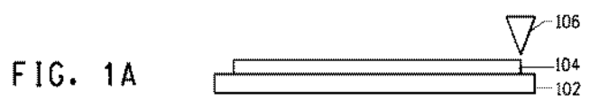
図1は、実用的製造手順を示す概略図である。第1に感光性ペーストはガラス基板上にコーティングされる。ディスペンサーを用いるコーティング方法(106)およびスクリーン印刷により導電性感光性ペースト(104)をガラス基板(102)上に完全にコーティングする(図1(A))。 FIG. 1 is a schematic diagram showing a practical manufacturing procedure. First, the photosensitive paste is coated on a glass substrate. The conductive photosensitive paste (104) is completely coated on the glass substrate (102) by a coating method (106) using a dispenser and screen printing (FIG. 1A).
次に、コーティングされた感光性ペーストを乾燥させる。感光性ペーストの層を乾燥させる場合、乾燥条件は特に限定されない。例えば、100℃で18〜20分間乾燥させてよい。同様に、コンベヤ型赤外線乾燥機を用いて感光性ペーストを乾燥させることもできる。 Next, the coated photosensitive paste is dried. When drying the layer of the photosensitive paste, the drying conditions are not particularly limited. For example, you may dry at 100 degreeC for 18-20 minutes. Similarly, the photosensitive paste can be dried using a conveyor-type infrared dryer.
次に、乾燥した感光性ペーストはパターン化される。パターン化処理において、乾燥した感光性ペーストは露光され現像される。露光プロセスにおいては、電極パターンを有するフォトマスク(108)が乾燥済み感光性ペースト(104)上に置かれ、これに対し紫外線(110)が照射される(図3(B))。 Next, the dried photosensitive paste is patterned. In the patterning process, the dried photosensitive paste is exposed and developed. In the exposure process, a photomask (108) having an electrode pattern is placed on the dried photosensitive paste (104) and irradiated with ultraviolet rays (110) (FIG. 3B).
露光条件は、感光性ペーストのタイプおよび感光性ペーストのフィルム厚によって異なる。例えば、200〜400μmの間隙が用いられる露光プロセスにおいては、100mJ/cm2〜2000mJ/cm2の紫外線を使用することが好ましい。照射期間は、好ましくは5〜200秒である。 The exposure conditions vary depending on the type of photosensitive paste and the film thickness of the photosensitive paste. For example, in the exposure process where a gap 200~400μm is used, it is preferable to use ultraviolet rays 100mJ / cm 2 ~2000mJ / cm 2 . The irradiation period is preferably 5 to 200 seconds.
現像はアルカリ溶液により行なうことができる。アルカリ溶液としては、0.4%の炭酸ナトリウム溶液を使用してよい。現像は、基板(102)上の露光済み感光性ペースト層(104)に対しアルカリ溶液(112)を噴霧することによって(図3(C))あるいは露光済み感光性ペースト(104)を有する基板(102)をアルカリ溶液中に浸漬することによって実施できる。 Development can be carried out with an alkaline solution. As the alkaline solution, a 0.4% sodium carbonate solution may be used. The development is performed by spraying an alkaline solution (112) onto the exposed photosensitive paste layer (104) on the substrate (102) (FIG. 3C) or a substrate having the exposed photosensitive paste (104) ( 102) can be carried out by dipping in an alkaline solution.
次に、パターン化された感光性ペーストは焼結される(図3(D))。組成物は、既定の温度プロファイルを有する焼結炉内で焼結可能である。焼結プロセス中の最高温度は好ましくは400〜600℃、またはより好ましくは500〜600℃である。焼結期間は好ましくは1〜3時間、好ましくは1.5時間である。 Next, the patterned photosensitive paste is sintered (FIG. 3D). The composition can be sintered in a sintering furnace having a predetermined temperature profile. The maximum temperature during the sintering process is preferably 400-600 ° C, or more preferably 500-600 ° C. The sintering period is preferably 1 to 3 hours, preferably 1.5 hours.
本発明において、焼成は空気雰囲気中で実施される。以上で指摘した通り、感光性ペーストの組成を制御することにより、空気焼成でさえ低抵抗の微細なパターンを形成することができる。本出願では、「空気中での焼成」または「空気焼成」とは、本質的に、焼成炉内の雰囲気の交換を伴わない焼成を意味し、より具体的には、これには焼成炉内の雰囲気の交換を伴わない焼成および炉内の5vol%以下の雰囲気の交換を伴う焼成の両方が含まれる。 In the present invention, the firing is performed in an air atmosphere. As pointed out above, by controlling the composition of the photosensitive paste, a fine pattern with low resistance can be formed even by air baking. In this application, “firing in air” or “air firing” essentially means firing without an exchange of atmosphere in the firing furnace, more specifically, in the firing furnace. Both the firing without the exchange of the atmosphere and the firing with the exchange of the atmosphere of 5 vol% or less in the furnace are included.
焼結および冷却プロセスの後、アドレス電極(114)を伴う基板(103)が得られる(図3(E))。 After the sintering and cooling process, a substrate (103) with address electrodes (114) is obtained (FIG. 3E).
銀ペーストと同じ要領で配線材料として使用した場合には、体積抵抗率を銀の抵抗率に比較して大幅(例えば100倍)に超過させることはできない。体積抵抗率が過度に大きくなった場合、抜本的な設計変更が必要となるため銅との置換は非常に困難になる。銀の体積抵抗率は、室温近くで1.6×10⁻⁶Ω・cmであることから、100倍の基準が設定されている場合、体積抵抗率は1.6×10⁻⁴Ω・cm以下であることが好ましい。本発明によると、空気ベーキングが実施される場合でも、導電性構成成分として銅を使用することによってこのような低抵抗電極を形成することが可能である。 When used as a wiring material in the same manner as the silver paste, the volume resistivity cannot be greatly exceeded (for example, 100 times) compared to the resistivity of silver. When the volume resistivity becomes excessively large, a drastic design change is required, so that replacement with copper becomes very difficult. Since the volume resistivity of silver is 1.6 × 10 −6 Ω · cm near room temperature, the volume resistivity is 1.6 × 10 −4 Ω · cm when a standard of 100 times is set. The following is preferable. According to the present invention, even when air baking is performed, such a low resistance electrode can be formed by using copper as a conductive component.
本発明は、電極を有する電子デバイスに応用可能であるが、特に用途がこれに限定されるわけではない。好ましくは、本発明は、PDPの背面パネルの電極に応用可能である。PDPの生産コストは、本発明を使用することによって削減できる。 The present invention can be applied to an electronic device having an electrode, but the application is not particularly limited thereto. Preferably, the present invention is applicable to an electrode of a PDP rear panel. The production cost of PDP can be reduced by using the present invention.
本発明について以下で実施例によりさらに詳細に説明する。実施例は単に例示を目的としたものであり、本発明を限定する意図はない。 The invention is explained in more detail below by means of examples. The examples are for illustrative purposes only and are not intended to limit the invention.
(A)銅およびホウ素粉末比の効果に関する試験
1.有機構成成分の調製
溶媒としてのテキサノール(2,2,4−トリメチル−1,3−ペンタンジオールモノイソブチレート)および有機結合剤として6,000〜7,000の分子量を有するアクリルポリマー結合剤を混合し、混合物を撹拌しながら100℃まで加熱した。全ての有機結合剤が溶解するまで混合物を加熱し撹拌した。得られた溶液を75℃まで冷却した。光重合開始剤としてEDAB(エチル4−ジメチルアミノベンゾエート)、DETX(ジエチルチオキサントン)およびChiba Specialty Chemicals製のIrgacure 907を添加し、安定剤としてTAOBN(1,4,4−トリメチル−2,3−ジアザビシクロ[3.2.2]−ノン−2−エン−N,N−ジクソイド(dixoide))を添加した。全ての固体が溶解するまで混合物を75℃で撹拌した。40ミクロンのフィルターを通して溶液を濾過し、冷却した。
(A) Test on effect of copper and boron powder ratio Preparation of organic components Texanol (2,2,4-trimethyl-1,3-pentanediol monoisobutyrate) as a solvent and an acrylic polymer binder having a molecular weight of 6,000 to 7,000 as an organic binder. Mix and heat the mixture to 100 ° C. with stirring. The mixture was heated and stirred until all the organic binder was dissolved. The resulting solution was cooled to 75 ° C. EDAB (ethyl 4-dimethylaminobenzoate), DETX (diethylthioxanthone) and Irgacure 907 from Chiba Specialty Chemicals were added as photopolymerization initiators, and TAOBN (1,4,4-trimethyl-2,3-diazabicyclo) was added as a stabilizer. [3.2.2] -non-2-ene-N, N-dixoid) was added. The mixture was stirred at 75 ° C. until all solids dissolved. The solution was filtered through a 40 micron filter and cooled.
2.銅およびホウ素ペーストの調製
2.42重量%のTMPEOTA(トリメチロールプロパンエトキシトリアクリレート)、2.42重量%のBASF製Laromer(登録商標)LR8967(ポリエチルアクリレートオリゴマー)および7.26重量%のSartomer(登録商標)SE399(ジペンタエリスリトールペンタアクリレート)からなる光重合モノマー、安定剤として0.26重量%のマロン酸、0.04重量%のシリコーン消泡剤(BYK Chemie、 BYK085)を、20.31重量%の上述の有機構成成分と黄色光の下で混合タンク内において混合して、ペーストを調製した。導電性粒子として、1.09重量%のビスマスフリット(日本山村硝子株式会社)、ホウ素粉末(H.C.Starck,Boron Amorphous I、D50=0.9μm)および銅粉末(Ultrafine Powder Technology、D50=1.0μm)を使用した。ホウ素粉末と銅粉末の量は、表1中に示されているように異なる実施例および比較例の間で変動した。実施例および比較例中で使用した量は、表1〜3に示されている。
2. Preparation of copper and boron pastes 2.42% by weight TMPEOTA (trimethylolpropane ethoxytriacrylate), 2.42% by weight Laromar® LR8967 (polyethyl acrylate oligomer) from BASF and 7.26% by weight Sartomer (1) a photopolymerization monomer composed of (registered trademark) SE399 (dipentaerythritol pentaacrylate), 0.26% by weight of malonic acid and 0.04% by weight of a silicone antifoaming agent (BYK Chemie, BYK085) as a stabilizer; A paste was prepared by mixing with 31% by weight of the above organic components in a mixing tank under yellow light. As conductive particles, 1.09% by weight of bismuth frit (Nihon Yamamura Glass Co., Ltd.), boron powder (HC Starck, Boron Amorphous I, D50 = 0.9 μm) and copper powder (Ultrafine Powder Technology, D50 = 1.0 μm) was used. The amounts of boron and copper powders varied between different examples and comparative examples as shown in Table 1. The amounts used in the examples and comparative examples are shown in Tables 1-3.
無機材料の粒子が有機材料により湿らされた状態となるまで、ペースト全体を混合した。3本ロールミルを用いて混合物を分散させた。 The entire paste was mixed until the inorganic material particles were wetted by the organic material. The mixture was dispersed using a three roll mill.
3.電極の調製
ペーストの調製および部品の製造中の汚れによる汚染は欠陥をもたらす結果となることが考えられるため、汚れによる汚染を回避するために予防措置を講じた。
3. Electrode Preparation Since contamination due to contamination during paste preparation and part manufacture could result in defects, precautions were taken to avoid contamination due to contamination.
3−1:コーティング
200〜400メッシュスクリーンを用いてスクリーン印刷することにより、ガラス基板に対して銅およびホウ素ペーストを塗布した。所望のフィルム厚を確実に得るため適切なスクリーンおよび黒色電極ペースト粘度を選択した。その後ペーストを熱風循環炉内において100℃で20分間乾燥して、4.5〜5.0μmの乾燥フィルム厚を有する銅およびホウ素電極を形成した。
3-1: Coating Copper and boron pastes were applied to a glass substrate by screen printing using a 200-400 mesh screen. Appropriate screen and black electrode paste viscosity were selected to ensure the desired film thickness. Thereafter, the paste was dried in a hot air circulating furnace at 100 ° C. for 20 minutes to form copper and boron electrodes having a dry film thickness of 4.5 to 5.0 μm.
3−2:紫外線パターン露光
乾燥したペーストを、平行紫外線放射源(照射:18〜20mW/cm2;露光:200〜2000mJ/cm2)を用いてフォトツールを介して露光した。
3-2: UV pattern exposure The dried paste was exposed through a photo tool using a parallel UV radiation source (irradiation: 18 to 20 mW / cm 2 ; exposure: 200 to 2000 mJ / cm 2 ).
3−3:現像
露光済み試料をコンベア上に置き、次に現像液として0.4重量%の炭酸ナトリウム水溶液を充填した噴霧式現像装置内に入れた。現像液を30℃の温度に保ち、10〜20psiで噴霧した。
3-3: Development The exposed sample was placed on a conveyor, and then placed in a spray developing device filled with 0.4% by weight sodium carbonate aqueous solution as a developer. The developer was kept at a temperature of 30 ° C. and sprayed at 10-20 psi.
現像時間は、以下の要領で決定した。第1に、現像液中で未露光の乾燥フィルムを洗浄する時間(TTC、Time To Clear)を、露光済みパターンを伴う試料の場合と同じ条件として、乾燥したその未露光試料を用いて印刷を行い、測定した。次に、露光されたパターンを伴う試料部品を、現像時間をTTCの1.5倍に設定して現像した。 The development time was determined as follows. First, the time for washing the unexposed dry film in the developer (TTC, Time To Clear) is set to the same conditions as in the case of the sample with the exposed pattern, and printing is performed using the dried unexposed sample. Performed and measured. Next, the sample part with the exposed pattern was developed with the development time set to 1.5 times TTC.
空気ジェットで余剰の水を吹き飛ばすことによって、現像済み試料を乾燥させた。 The developed sample was dried by blowing off excess water with an air jet.
3−4:焼結
1.5時間のプロファイルを用いて空気中でベルト炉内で焼結させることによって、590℃のピーク温度に達した(第1回焼結)。
3-4: Sintering A peak temperature of 590 ° C. was reached by sintering in a belt furnace in air using a 1.5 hour profile (first sintering).
有機構成成分の含有量およびさまざまな銅粉末サイズは一定に保ち、ホウ素の重量と銅およびホウ素を組み合わせた重量との比([B]/[Cu+B])を、5%から50%まで変動させ、焼成した部品の表面抵抗を測定した。 Keeping the organic component content and various copper powder sizes constant, the ratio of the weight of boron to the combined weight of copper and boron ([B] / [Cu + B]) varied from 5% to 50% The surface resistance of the fired parts was measured.
表面抵抗の測定用として、ポリ#380メッシュスクリーンを用いてスライドガラス上に試料ペーストをスクリーン印刷して40mm×40mmの正方形の印刷済み部域を形成することで、供試体を調製した。部品を乾燥させ、フォトマスクを使用せずに完全に露光し、その後焼成した。40mm×40mmの部域の対角線を横断して表面上に2つのプローブを適用することによって、焼成済みフィルムの表面抵抗を測定した。この測定のためには、焼成済みフィルムの厚みを3〜5μmの範囲に調整した。 For measurement of surface resistance, a specimen was prepared by screen printing a sample paste on a slide glass using a poly # 380 mesh screen to form a square printed area of 40 mm × 40 mm. The parts were dried, fully exposed without using a photomask, and then fired. The surface resistance of the fired film was measured by applying two probes on the surface across a 40 mm × 40 mm area diagonal. For this measurement, the thickness of the fired film was adjusted to a range of 3 to 5 μm.
以下の方法によって、ライン形成を評価した。パターン露光を伴う現像済み試料片を目視により調べて、現像後に微細なラインが残っているか否かを判定した。より具体的には、試料部品を、100μmのラインパターンフォトマスクを用いて800mJ/cm2で露光し、その後、焼成済みフィルムの厚みを3〜5μmに調整しながら、TTCの1.5倍の現像時間で現像した。 Line formation was evaluated by the following method. The developed sample piece with pattern exposure was examined visually to determine whether fine lines remained after development. More specifically, the sample part was exposed at 800 mJ / cm 2 using a 100 μm line pattern photomask, and then the thickness of the fired film was adjusted to 3 to 5 μm while being 1.5 times the TTC. Developed with development time.
現像の後100μmのラインが残っていた場合、これをOK(合格)と評定した。しかし100μmのラインが洗い流されるかまたは数多くの配線破断が観察された場合には、NG(不合格)と評定した。 If a 100 μm line remained after development, it was rated OK. However, if the 100 μm line was washed away or numerous wire breaks were observed, it was rated as NG (failed).
空気焼成条件下で、銅粉末は酸化され易いが、ホウ素重量比が15%および17.5%の試料の場合、表面抵抗は1.0Ω未満であり、ホウ素の存在によって酸化が事実上抑制されることがわかった。5重量%のホウ素含有量を有する試料の場合、酸化が進行したため抵抗は1MΩを上回り、表面抵抗は非常に大きくなった。一方、35重量%および50重量%のホウ素含有量を有する試料において、表面抵抗は、装置の測定上限(100MΩ)よりも大きいものであった。許容抵抗値を100Ωに設定した場合、ホウ素重量と銅とホウ素の組合せ重量との比について、5重量%という値は過小であり、35重量%の値は過大であるとみなすことができる。図2は、ホウ素含有量と表面抵抗の関係を示すグラフである。 Under air firing conditions, copper powder is susceptible to oxidation, but for samples with boron weight ratios of 15% and 17.5%, the surface resistance is less than 1.0Ω and the presence of boron effectively suppresses oxidation. I found out. In the case of the sample having a boron content of 5% by weight, since the oxidation progressed, the resistance exceeded 1 MΩ and the surface resistance became very large. On the other hand, in the samples having a boron content of 35% by weight and 50% by weight, the surface resistance was larger than the measurement upper limit (100 MΩ) of the apparatus. When the allowable resistance value is set to 100Ω, the value of 5% by weight is excessively small and the value of 35% by weight can be regarded as excessive with respect to the ratio between the boron weight and the combined weight of copper and boron. FIG. 2 is a graph showing the relationship between boron content and surface resistance.

(B)銅粉末の直径の効果に関する試験
表2に示されているように、有機構成成分の含有量および銅とホウ素の組合せ重量に対するホウ素の重量の割合([B]/[Cu+B]=17.5重量%)を一定に保ち、銅粉末の平均粒度(D50)を変動させ、焼成した部品内で表面抵抗を測定した。3μmという平均粒度(D50)を有する銅粉末を使用した場合、表面抵抗は34.1Ωまで増大し、このような大きな粒度の銅粉末で所望の低い抵抗値を得ることは困難であることがわかった。
(B) Test on Effect of Copper Powder Diameter As shown in Table 2, the ratio of the weight of boron to the content of organic components and the combined weight of copper and boron ([B] / [Cu + B] = 17 0.5% by weight), the average particle size (D50) of the copper powder was varied, and the surface resistance was measured in the fired parts. When copper powder having an average particle size (D50) of 3 μm is used, the surface resistance increases to 34.1 Ω, and it is found that it is difficult to obtain a desired low resistance value with such a large particle size copper powder. It was.
(C)有機および無機組成物の効果に関する試験
銅とホウ素の組合せ重量に対するホウ素の重量の割合([B]/[Cu+B]を17.5重量%で一定に保ち、D50=1.1の銅粉末を用いて、無機構成成分および有機構成成分の量または有機構成成分中のモノマーの量を変動させることによって表3中に示したペーストを調製し、ベーキング後の体積抵抗をフォトパターン化およびパターン化されたラインとの関係において決定した。
(C) Test on effect of organic and inorganic composition Ratio of boron weight to combined weight of copper and boron ([B] / [Cu + B] kept constant at 17.5% by weight, D50 = 1.1 copper Using the powder, the paste shown in Table 3 was prepared by varying the amount of inorganic and organic components or the amount of monomer in the organic component, and the volume resistance after baking was photopatterned and patterned. In relation to the normalized lines.
概してラインを形成せずに測定された表面抵抗について、優れた値が得られた。無機/有機組成物の詳細を調査すると、100μmのラインのパターン形成は、[無機構成成分の重量]/[有機構成成分の重量]の値が3.5以下である場合に優れている傾向にあった。ライン形成は同様に、[モノマー重量]/[無機構成成分の重量]が0.1〜0.3の範囲内であった場合にも優れている傾向にあった。表3に示す通り、[無機構成成分の重量]/[有機構成成分の重量]がさらに小さくなった場合に、抵抗率は増大した。[モノマーの重量]/[有機構成成分の重量]が0.3以上に上昇した場合に、ラインの形成を良好に行うことはできたが、抵抗は増大し、表面粘着性が増大する傾向にあった。 In general, excellent values were obtained for the surface resistance measured without forming a line. When the details of the inorganic / organic composition are investigated, the pattern formation of a 100 μm line tends to be excellent when the value of [weight of inorganic component] / [weight of organic component] is 3.5 or less. there were. Similarly, line formation tended to be excellent when [monomer weight] / [inorganic constituent weight] was in the range of 0.1 to 0.3. As shown in Table 3, the resistivity increased when [weight of inorganic constituent] / [weight of organic constituent] was further reduced. When [weight of monomer] / [weight of organic component] increased to 0.3 or more, the line could be formed satisfactorily, but the resistance increased and the surface tackiness tended to increase. there were.
体積抵抗率は、以下の方法を用いて評価した。 The volume resistivity was evaluated using the following method.
体積抵抗率のためには、幅400μm長さ14.7mmのラインパターンを有するフォトマスクを用いて露光し、現像し、焼成することによって形成されたパターンについて、抵抗を測定した。その後、ライン幅およびフィルム厚から体積抵抗率を計算した。 For volume resistivity, resistance was measured for a pattern formed by exposing, developing, and firing using a photomask having a line pattern having a width of 400 μm and a length of 14.7 mm. Thereafter, the volume resistivity was calculated from the line width and the film thickness.
1.感光性ペーストを空気中で焼成することで形成される電極であって、前記ペーストが、銅粉末、ホウ素粉末およびガラスフリットを含む無機構成成分と、光重合開始剤、モノマーおよび有機ビヒクルを含む有機構成成分とを含み、銅粉末の平均粒度が2.5μm以下であり、銅粉末とホウ素粉末の総量に基づくホウ素粉末の含有量が8〜25重量%である、電極。 1. An electrode formed by firing a photosensitive paste in air, wherein the paste includes an inorganic component including copper powder, boron powder, and glass frit, and an organic including a photopolymerization initiator, a monomer, and an organic vehicle. And an electrode having an average particle size of 2.5 μm or less and a content of boron powder based on the total amount of copper powder and boron powder of 8 to 25% by weight.
2.前記ホウ素粉末の平均粒度が3μm以下であり、前記電極のフィルム厚が1〜4μmである、前記1に記載の電極。 2. 2. The electrode according to 1 above, wherein the average particle size of the boron powder is 3 μm or less, and the film thickness of the electrode is 1 to 4 μm.
3.プラズマディスプレイパネル用に使用され、体積抵抗率が1.6×10⁻⁴Ω・cmである、前記1に記載の電極。 3. 2. The electrode according to 1 above, which is used for a plasma display panel and has a volume resistivity of 1.6 × 10 −4 Ω · cm.
4.プラズマディスプレイパネル用の電極の製造方法であって、 4). A method of manufacturing an electrode for a plasma display panel,
銅粉末、ホウ素粉末およびガラスフリットを含む無機構成成分と、光重合開始剤、モノマーおよび有機ビヒクルを含む有機構成成分とを含み、前記銅粉末の平均粒度が2.5μm以下であり、銅粉末とホウ素粉末の総量に基づくホウ素粉末の含有量が8〜25重量%である感光性ペーストを塗布するステップと; An inorganic component containing copper powder, boron powder and glass frit, and an organic component containing a photopolymerization initiator, a monomer and an organic vehicle, the copper powder having an average particle size of 2.5 μm or less, Applying a photosensitive paste having a boron powder content of 8 to 25% by weight based on the total amount of boron powder;
前記塗布した感光性ペーストを乾燥させるステップと; Drying the applied photosensitive paste;
前記乾燥した感光性ペーストを露光するステップと; Exposing the dried photosensitive paste;
前記露光した感光性ペーストを現像するステップと; Developing the exposed photosensitive paste;
前記現像した感光性ペーストを空気中で焼成して電極パターンを形成するステップと、 Baking the developed photosensitive paste in air to form an electrode pattern;
を含む方法。 Including methods.
5.前記ホウ素粉末の平均粒度が3μm以下であり、前記電極のフィルム厚が1〜4μmである、前記4に記載の電極の製造方法。 5. 5. The method for producing an electrode according to 4, wherein the boron powder has an average particle size of 3 μm or less and the film thickness of the electrode is 1 to 4 μm.
6.前記無機構成成分の含有量に関して前記モノマーの含有量が8〜35重量%である、前記4に記載の電極の製造方法。 6). 5. The method for producing an electrode according to 4, wherein the content of the monomer is 8 to 35% by weight with respect to the content of the inorganic constituent component.
7.前記感光性ペースト中の[無機構成成分重量]/[有機構成成分重量]比が1.2〜3.5であり、ここで前記無機構成成分重量は前記無機構成成分の総重量を意味し、前記有機構成成分重量は溶媒を除いた前記有機構成成分の総重量を意味し、かつ[モノマー重量]/[無機構成成分重量]比が0.1〜0.3である、前記4に記載の電極の製造方法。 7). The [inorganic component weight] / [organic component weight] ratio in the photosensitive paste is 1.2 to 3.5, wherein the inorganic component weight means the total weight of the inorganic component, 5. The organic component weight means the total weight of the organic component excluding the solvent, and the [monomer weight] / [inorganic component weight] ratio is 0.1 to 0.3. Electrode manufacturing method.
Claims (2)
銅粉末、ホウ素粉末およびガラスフリットを含む無機構成成分と、光重合開始剤、モノマーおよび有機ビヒクルを含む有機構成成分とを含み、前記銅粉末の平均粒度が2.5μm以下であり、銅粉末とホウ素粉末の総量に基づくホウ素粉末の含有量が8〜25重量%である感光性ペーストを塗布するステップと;
前記塗布した感光性ペーストを乾燥させるステップと;
前記乾燥した感光性ペーストを露光するステップと;
前記露光した感光性ペーストを現像するステップと;
前記現像した感光性ペーストを空気中で焼成して電極パターンを形成するステップと、
を含む方法。 A method of manufacturing an electrode for a plasma display panel , wherein the surface resistance of the electrode is 100Ω or less,
An inorganic component containing copper powder, boron powder and glass frit, and an organic component containing a photopolymerization initiator, a monomer and an organic vehicle, the copper powder having an average particle size of 2.5 μm or less, Applying a photosensitive paste having a boron powder content of 8 to 25% by weight based on the total amount of boron powder;
Drying the applied photosensitive paste;
Exposing the dried photosensitive paste;
Developing the exposed photosensitive paste;
Baking the developed photosensitive paste in air to form an electrode pattern;
Including methods.
Applications Claiming Priority (3)
| Application Number | Priority Date | Filing Date | Title |
|---|---|---|---|
| US12/496,920 US8129088B2 (en) | 2009-07-02 | 2009-07-02 | Electrode and method for manufacturing the same |
| US12/496,920 | 2009-07-02 | ||
| PCT/US2010/040719 WO2011002964A1 (en) | 2009-07-02 | 2010-07-01 | Electrode and method of manufacturing the same |
Publications (3)
| Publication Number | Publication Date |
|---|---|
| JP2012532420A JP2012532420A (en) | 2012-12-13 |
| JP2012532420A5 JP2012532420A5 (en) | 2013-07-18 |
| JP5654588B2 true JP5654588B2 (en) | 2015-01-14 |
Family
ID=42537876
Family Applications (1)
| Application Number | Title | Priority Date | Filing Date |
|---|---|---|---|
| JP2012517905A Active JP5654588B2 (en) | 2009-07-02 | 2010-07-01 | Electrode and manufacturing method thereof |
Country Status (7)
| Country | Link |
|---|---|
| US (1) | US8129088B2 (en) |
| EP (1) | EP2449571A1 (en) |
| JP (1) | JP5654588B2 (en) |
| KR (1) | KR20120032551A (en) |
| CN (1) | CN102473563B (en) |
| TW (1) | TW201115593A (en) |
| WO (1) | WO2011002964A1 (en) |
Families Citing this family (21)
| Publication number | Priority date | Publication date | Assignee | Title |
|---|---|---|---|---|
| US20110083874A1 (en) * | 2009-10-09 | 2011-04-14 | E. I. Du Pont De Nemours And Company | Electrode and method for manufacturing the same |
| US8728355B2 (en) * | 2011-01-14 | 2014-05-20 | E. I. Du Pont De Nemours And Company | Electrode and method for manufacturing the same |
| US8709294B2 (en) * | 2011-01-28 | 2014-04-29 | E. I. Du Pont De Nemours And Company | Electrode and method for manufacturing the same |
| US8647815B1 (en) | 2012-07-26 | 2014-02-11 | E I Du Pont De Nemours And Company | Method of manufacturing copper electrode |
| EP2957155B1 (en) * | 2013-02-18 | 2019-09-11 | Orbotech Ltd. | Two-step, direct- write laser metallization |
| US10622244B2 (en) | 2013-02-18 | 2020-04-14 | Orbotech Ltd. | Pulsed-mode direct-write laser metallization |
| US10537027B2 (en) | 2013-08-02 | 2020-01-14 | Orbotech Ltd. | Method producing a conductive path on a substrate |
| US20150197645A1 (en) * | 2014-01-16 | 2015-07-16 | E I Du Pont De Nemours And Company | Method of manufacturing non-firing type electrode |
| DE112014006907T5 (en) * | 2014-08-28 | 2017-06-08 | E.I. Du Pont De Nemours And Company | Copper-containing conductive pastes and electrodes made therefrom |
| CN106605270B (en) | 2014-08-28 | 2019-03-08 | E.I.内穆尔杜邦公司 | Cupric electrocondution slurry and thus manufactured electrode |
| DE112014006903B4 (en) | 2014-08-28 | 2022-07-21 | Solar Paste, Llc | Solar cells with copper electrodes |
| US10193004B2 (en) | 2014-10-19 | 2019-01-29 | Orbotech Ltd. | LIFT printing of conductive traces onto a semiconductor substrate |
| WO2016075743A1 (en) | 2014-11-10 | 2016-05-19 | 大研化学工業株式会社 | Conductive paste for atmospheric firing and method for producing same |
| US10633758B2 (en) | 2015-01-19 | 2020-04-28 | Orbotech Ltd. | Printing of three-dimensional metal structures with a sacrificial support |
| US9966480B2 (en) * | 2015-04-28 | 2018-05-08 | Samsung Sdi Co., Ltd. | Electrode composition, electrode manufactured using the same, and solar cell |
| JP6784350B2 (en) | 2015-11-22 | 2020-11-11 | オルボテック リミテッド | Controlling surface properties of printed 3D structures |
| TW201901887A (en) | 2017-05-24 | 2019-01-01 | 以色列商奧寶科技股份有限公司 | Electrical interconnection circuit components on the substrate without prior patterning |
| KR102367615B1 (en) * | 2017-10-12 | 2022-02-25 | 한국전자기술연구원 | Conductive paste composition, method for preparing the composition and electrode formed by the composition |
| US10515737B2 (en) * | 2017-10-12 | 2019-12-24 | Korea Electronics Technology Institute | Conductive paste composition, method for preparing the composition and electrode formed by the composition |
| KR102367611B1 (en) * | 2017-10-12 | 2022-02-25 | 한국전자기술연구원 | Conductive paste composition, method for preparing the composition and electrode formed by the composition |
| KR102608305B1 (en) * | 2021-11-25 | 2023-11-30 | 한국화학연구원 | Positive photosensitive paste composition, electrode provided with conductive pattern using the same, and manufacturing method thereof |
Family Cites Families (30)
| Publication number | Priority date | Publication date | Assignee | Title |
|---|---|---|---|---|
| NL101499C (en) | 1951-08-20 | |||
| US2875047A (en) | 1955-01-19 | 1959-02-24 | Oster Gerald | Photopolymerization with the formation of coherent plastic masses |
| US2850445A (en) | 1955-01-19 | 1958-09-02 | Oster Gerald | Photopolymerization |
| US3074974A (en) | 1957-12-06 | 1963-01-22 | Monsanto Chemicals | Method for the preparation of diglycidyl ether of tetrachlorobisphenol-a |
| US3097097A (en) | 1959-02-12 | 1963-07-09 | Gisela K Oster | Photo degrading of gel systems and photographic production of reliefs therewith |
| NL254306A (en) | 1959-08-07 | |||
| GB1090142A (en) | 1965-02-26 | 1967-11-08 | Agfa Gevaert Nv | Photochemical insolubilisation of polymers |
| US3479185A (en) | 1965-06-03 | 1969-11-18 | Du Pont | Photopolymerizable compositions and layers containing 2,4,5-triphenylimidazoyl dimers |
| US3380381A (en) * | 1965-08-06 | 1968-04-30 | Western Printing Mach Co | Rotary press printing cylinder for clamping flexible plates |
| US3549367A (en) | 1968-05-24 | 1970-12-22 | Du Pont | Photopolymerizable compositions containing triarylimidazolyl dimers and p-aminophenyl ketones |
| US4122232A (en) * | 1975-04-21 | 1978-10-24 | Engelhard Minerals & Chemicals Corporation | Air firable base metal conductors |
| US4070517A (en) * | 1976-07-08 | 1978-01-24 | Beckman Instruments, Inc. | Low fired conductive compositions |
| US4162162A (en) | 1978-05-08 | 1979-07-24 | E. I. Du Pont De Nemours And Company | Derivatives of aryl ketones and p-dialkyl-aminoarylaldehydes as visible sensitizers of photopolymerizable compositions |
| JPS5874030A (en) * | 1981-10-28 | 1983-05-04 | ティーディーケイ株式会社 | Electronic part, conductive film composition and method of producing same |
| US5047313A (en) * | 1989-08-21 | 1991-09-10 | E. I. Du Pont De Nemours And Company | Photosensitive semi-aqueous developable copper conductor composition |
| JP2841586B2 (en) * | 1989-12-04 | 1998-12-24 | 大同特殊鋼株式会社 | Conductive paste |
| JPH06349316A (en) * | 1993-06-11 | 1994-12-22 | Tdk Corp | Conductive paste |
| JP3079930B2 (en) * | 1995-01-23 | 2000-08-21 | 株式会社村田製作所 | Porcelain capacitors |
| US5851732A (en) | 1997-03-06 | 1998-12-22 | E. I. Du Pont De Nemours And Company | Plasma display panel device fabrication utilizing black electrode between substrate and conductor electrode |
| JPH11242930A (en) * | 1997-12-03 | 1999-09-07 | Toray Ind Inc | Manufacture of electrode and manufacture of member for plasma display panel |
| KR20050122498A (en) * | 2004-06-24 | 2005-12-29 | 삼성에스디아이 주식회사 | A photosensitive paste composition, the pdp electrode prepared therefrom and a pdp comprising the pdp electrode |
| JP2006030853A (en) * | 2004-07-21 | 2006-02-02 | Taiyo Ink Mfg Ltd | Photosensitive paste and baked product pattern formed using the same |
| JP4760709B2 (en) * | 2004-07-22 | 2011-08-31 | 東レ株式会社 | Photosensitive paste and method for producing display panel member |
| US7135267B2 (en) * | 2004-08-06 | 2006-11-14 | E. I. Du Pont De Nemours And Company | Aqueous developable photoimageable compositions for use in photo-patterning methods |
| KR100658714B1 (en) * | 2004-11-30 | 2006-12-15 | 삼성에스디아이 주식회사 | Photo-sensitive composition, photo-sensitive paste composition for barrier ribs comprising the same, and method for preparing barrier ribs for plasma display panel |
| JP2007012371A (en) * | 2005-06-29 | 2007-01-18 | E I Du Pont De Nemours & Co | Method for manufacturing conductive composition and rear substrate of plasma display |
| US7655864B2 (en) * | 2006-07-13 | 2010-02-02 | E.I Du Pont De Nemours And Company | Photosensitive conductive paste for electrode formation and electrode |
| KR100829667B1 (en) * | 2006-09-07 | 2008-05-16 | 엘지전자 주식회사 | Electrode paste composite, up-board structure of plasma display panel and manufacturing method manufactured by using the same |
| KR100852705B1 (en) | 2006-09-15 | 2008-08-19 | 삼성에스디아이 주식회사 | Composition of electrode paste and plasma display panel using the same |
| US7887992B2 (en) * | 2008-12-23 | 2011-02-15 | E. I. Du Pont De Nemours And Company | Photosensitive paste and process for production of pattern using the same |
-
2009
- 2009-07-02 US US12/496,920 patent/US8129088B2/en active Active
-
2010
- 2010-07-01 CN CN201080027528.8A patent/CN102473563B/en active Active
- 2010-07-01 EP EP10735368A patent/EP2449571A1/en not_active Withdrawn
- 2010-07-01 JP JP2012517905A patent/JP5654588B2/en active Active
- 2010-07-01 KR KR1020127002809A patent/KR20120032551A/en not_active Application Discontinuation
- 2010-07-01 WO PCT/US2010/040719 patent/WO2011002964A1/en active Application Filing
- 2010-07-01 TW TW099121709A patent/TW201115593A/en unknown
Also Published As
| Publication number | Publication date |
|---|---|
| EP2449571A1 (en) | 2012-05-09 |
| WO2011002964A1 (en) | 2011-01-06 |
| TW201115593A (en) | 2011-05-01 |
| JP2012532420A (en) | 2012-12-13 |
| CN102473563B (en) | 2014-07-23 |
| US8129088B2 (en) | 2012-03-06 |
| US20110003246A1 (en) | 2011-01-06 |
| KR20120032551A (en) | 2012-04-05 |
| CN102473563A (en) | 2012-05-23 |
Similar Documents
| Publication | Publication Date | Title |
|---|---|---|
| JP5654588B2 (en) | Electrode and manufacturing method thereof | |
| US20120255765A1 (en) | Electrode and method for manufacturing the same | |
| JP3779297B2 (en) | Photoformable black electrode and black electrode composition | |
| US7608784B2 (en) | Photosensitive conductive paste for electrode formation and electrode | |
| US20060071202A1 (en) | Photosensitive paste composition | |
| JP2006108072A (en) | Positive type photosensitive paste composition for plasma display panel electrode formation, film manufactured using the same, plasma display panel electrode and plasma display panel | |
| KR101100490B1 (en) | Electrode paste for plasma display panel and black bus electrode for plasma display panel | |
| JP2006339139A (en) | Black conductive thick-film composition, black electrode, and formation method thereof | |
| JP2012216827A (en) | Manufacturing method of solar cell electrode and solar cell electrode manufactured by using the same | |
| JP2012513624A (en) | Photosensitive paste and pattern production method using the same | |
| KR20090034379A (en) | Photosensitive conductive paste for electrode formation and electrode | |
| US8728355B2 (en) | Electrode and method for manufacturing the same | |
| DE60204711T2 (en) | AQUEOUS DEVELOPABLE, LIGHT-SENSITIVE LAYER-LAYER COMPOSITION COMPOSITIONS FOR THE PRODUCTION OF BLACK ELECTRODES | |
| JP5303127B2 (en) | Conductive composition for black bus electrode and front panel of plasma display panel | |
| JP2010237573A (en) | Pattern forming method using laser | |
| US7645564B2 (en) | Polymer solutions, aqueous developable thick film compositions, processes of making and electrodes formed thereof | |
| JP2011524023A (en) | Photosensitive paste and sintered layer | |
| US8709294B2 (en) | Electrode and method for manufacturing the same | |
| JP5421391B2 (en) | Front electrode of PDP | |
| JP2011503806A (en) | Conductive composition for black bus electrode and front panel of plasma display panel | |
| JP2001084912A (en) | Plasma display panel | |
| JP2014063705A (en) | Method of manufacturing pdp bus electrode | |
| US20140061543A1 (en) | Method of manufacturing non-firing type electrode using photosensitive paste |
Legal Events
| Date | Code | Title | Description |
|---|---|---|---|
| A521 | Request for written amendment filed |
Free format text: JAPANESE INTERMEDIATE CODE: A523 Effective date: 20130603 |
|
| A621 | Written request for application examination |
Free format text: JAPANESE INTERMEDIATE CODE: A621 Effective date: 20130603 |
|
| A131 | Notification of reasons for refusal |
Free format text: JAPANESE INTERMEDIATE CODE: A131 Effective date: 20131126 |
|
| A521 | Request for written amendment filed |
Free format text: JAPANESE INTERMEDIATE CODE: A523 Effective date: 20140218 |
|
| TRDD | Decision of grant or rejection written | ||
| A01 | Written decision to grant a patent or to grant a registration (utility model) |
Free format text: JAPANESE INTERMEDIATE CODE: A01 Effective date: 20141021 |
|
| A61 | First payment of annual fees (during grant procedure) |
Free format text: JAPANESE INTERMEDIATE CODE: A61 Effective date: 20141120 |
|
| R150 | Certificate of patent or registration of utility model |
Ref document number: 5654588 Country of ref document: JP Free format text: JAPANESE INTERMEDIATE CODE: R150 |
|
| R250 | Receipt of annual fees |
Free format text: JAPANESE INTERMEDIATE CODE: R250 |
|
| R250 | Receipt of annual fees |
Free format text: JAPANESE INTERMEDIATE CODE: R250 |
|
| R250 | Receipt of annual fees |
Free format text: JAPANESE INTERMEDIATE CODE: R250 |
|
| R250 | Receipt of annual fees |
Free format text: JAPANESE INTERMEDIATE CODE: R250 |
|
| R250 | Receipt of annual fees |
Free format text: JAPANESE INTERMEDIATE CODE: R250 |
|
| R250 | Receipt of annual fees |
Free format text: JAPANESE INTERMEDIATE CODE: R250 |