JP5648001B2 - Gas sensor processing equipment - Google Patents
Gas sensor processing equipment Download PDFInfo
- Publication number
- JP5648001B2 JP5648001B2 JP2012004568A JP2012004568A JP5648001B2 JP 5648001 B2 JP5648001 B2 JP 5648001B2 JP 2012004568 A JP2012004568 A JP 2012004568A JP 2012004568 A JP2012004568 A JP 2012004568A JP 5648001 B2 JP5648001 B2 JP 5648001B2
- Authority
- JP
- Japan
- Prior art keywords
- voltage
- detection element
- detection
- shift
- index
- Prior art date
- Legal status (The legal status is an assumption and is not a legal conclusion. Google has not performed a legal analysis and makes no representation as to the accuracy of the status listed.)
- Active
Links
Images


Classifications
-
- G—PHYSICS
- G01—MEASURING; TESTING
- G01N—INVESTIGATING OR ANALYSING MATERIALS BY DETERMINING THEIR CHEMICAL OR PHYSICAL PROPERTIES
- G01N27/00—Investigating or analysing materials by the use of electric, electrochemical, or magnetic means
- G01N27/26—Investigating or analysing materials by the use of electric, electrochemical, or magnetic means by investigating electrochemical variables; by using electrolysis or electrophoresis
- G01N27/403—Cells and electrode assemblies
- G01N27/406—Cells and probes with solid electrolytes
- G01N27/407—Cells and probes with solid electrolytes for investigating or analysing gases
- G01N27/409—Oxygen concentration cells
-
- F—MECHANICAL ENGINEERING; LIGHTING; HEATING; WEAPONS; BLASTING
- F02—COMBUSTION ENGINES; HOT-GAS OR COMBUSTION-PRODUCT ENGINE PLANTS
- F02D—CONTROLLING COMBUSTION ENGINES
- F02D41/00—Electrical control of supply of combustible mixture or its constituents
- F02D41/02—Circuit arrangements for generating control signals
- F02D41/14—Introducing closed-loop corrections
- F02D41/1438—Introducing closed-loop corrections using means for determining characteristics of the combustion gases; Sensors therefor
- F02D41/1444—Introducing closed-loop corrections using means for determining characteristics of the combustion gases; Sensors therefor characterised by the characteristics of the combustion gases
- F02D41/1454—Introducing closed-loop corrections using means for determining characteristics of the combustion gases; Sensors therefor characterised by the characteristics of the combustion gases the characteristics being an oxygen content or concentration or the air-fuel ratio
- F02D41/1455—Introducing closed-loop corrections using means for determining characteristics of the combustion gases; Sensors therefor characterised by the characteristics of the combustion gases the characteristics being an oxygen content or concentration or the air-fuel ratio with sensor resistivity varying with oxygen concentration
-
- F—MECHANICAL ENGINEERING; LIGHTING; HEATING; WEAPONS; BLASTING
- F02—COMBUSTION ENGINES; HOT-GAS OR COMBUSTION-PRODUCT ENGINE PLANTS
- F02D—CONTROLLING COMBUSTION ENGINES
- F02D41/00—Electrical control of supply of combustible mixture or its constituents
- F02D41/02—Circuit arrangements for generating control signals
- F02D41/14—Introducing closed-loop corrections
- F02D41/1438—Introducing closed-loop corrections using means for determining characteristics of the combustion gases; Sensors therefor
- F02D41/1493—Details
- F02D41/1494—Control of sensor heater
-
- F—MECHANICAL ENGINEERING; LIGHTING; HEATING; WEAPONS; BLASTING
- F02—COMBUSTION ENGINES; HOT-GAS OR COMBUSTION-PRODUCT ENGINE PLANTS
- F02D—CONTROLLING COMBUSTION ENGINES
- F02D41/00—Electrical control of supply of combustible mixture or its constituents
- F02D41/02—Circuit arrangements for generating control signals
- F02D41/14—Introducing closed-loop corrections
- F02D41/1438—Introducing closed-loop corrections using means for determining characteristics of the combustion gases; Sensors therefor
- F02D41/1493—Details
- F02D41/1495—Detection of abnormalities in the air/fuel ratio feedback system
-
- G—PHYSICS
- G01—MEASURING; TESTING
- G01N—INVESTIGATING OR ANALYSING MATERIALS BY DETERMINING THEIR CHEMICAL OR PHYSICAL PROPERTIES
- G01N27/00—Investigating or analysing materials by the use of electric, electrochemical, or magnetic means
- G01N27/26—Investigating or analysing materials by the use of electric, electrochemical, or magnetic means by investigating electrochemical variables; by using electrolysis or electrophoresis
- G01N27/403—Cells and electrode assemblies
- G01N27/406—Cells and probes with solid electrolytes
- G01N27/4065—Circuit arrangements specially adapted therefor
-
- F—MECHANICAL ENGINEERING; LIGHTING; HEATING; WEAPONS; BLASTING
- F02—COMBUSTION ENGINES; HOT-GAS OR COMBUSTION-PRODUCT ENGINE PLANTS
- F02D—CONTROLLING COMBUSTION ENGINES
- F02D41/00—Electrical control of supply of combustible mixture or its constituents
- F02D41/02—Circuit arrangements for generating control signals
- F02D41/04—Introducing corrections for particular operating conditions
- F02D41/042—Introducing corrections for particular operating conditions for stopping the engine
Description
本発明は、特定ガスのガス濃度を検出するガスセンサの出力を処理するガスセンサ処理装置に関する。 The present invention relates to a gas sensor processing apparatus that processes an output of a gas sensor that detects a gas concentration of a specific gas.
従来より、車両の内燃機関の排気管に設置し、空燃比を制御するためなどの目的で、排気ガス中の特定ガスのガス濃度を検出するガスセンサが用いられており、例えば、酸素濃度を検出する酸素センサや窒素酸化物(NOx)の濃度を検出するNOxセンサなどが知られている。これらのガスセンサでは、ジルコニア(酸化ジルコニウム)を主体とした固体電解質体を検出素子として用いることが多い。この固体電解質体は、おおむね600℃以上の高温状態(活性化状態)で良好な酸素イオン伝導性を示す。また、検出素子の素子インピーダンス(内部抵抗)が、その素子温度に応じて変化することを利用して、検出素子の温度を検出したり、検出素子を活性化状態内の一定温度に維持すべく、素子インピーダンスが目標インピーダンスになるように、別途設けたヒータへの通電をフィードバック制御することが行われている。 Conventionally, a gas sensor that detects the gas concentration of a specific gas in exhaust gas has been used for the purpose of controlling the air-fuel ratio by installing it in the exhaust pipe of an internal combustion engine of a vehicle, for example, detecting the oxygen concentration. An oxygen sensor that detects the concentration of nitrogen oxide (NOx) is known. In these gas sensors, a solid electrolyte body mainly composed of zirconia (zirconium oxide) is often used as a detection element. This solid electrolyte body exhibits good oxygen ion conductivity in a high temperature state (activated state) of approximately 600 ° C. or higher. Further, by utilizing the fact that the element impedance (internal resistance) of the detection element changes according to the element temperature, it is necessary to detect the temperature of the detection element or to maintain the detection element at a constant temperature within the activated state. In order for the element impedance to be the target impedance, feedback control of energization to a separately provided heater is performed.
ところで、このようなガスセンサの検出素子では、使用等による劣化で素子インピーダンス(内部抵抗)が徐々に増加する。このため、劣化した検出素子では、劣化前に比して、同一温度とした場合の素子インピーダンス(内部抵抗)が相対的に高くなる。従って、正確に温度を検知することが難しい。また、上述のヒータへのフィードバック制御を行うと、素子インピーダンスを目標インピーダンスに近づけるべく、素子インピーダンスを下げる方向、即ち、素子温度を上げる方向に制御がなされる。このため、素子温度が素子インピーダンスの増加に伴って上昇しこの温度上昇により、検出素子の劣化が促進されるなどの問題があった。 By the way, in the detection element of such a gas sensor, element impedance (internal resistance) gradually increases due to deterioration due to use or the like. For this reason, in the detection element which deteriorated, the element impedance (internal resistance) at the same temperature is relatively higher than before the deterioration. Therefore, it is difficult to accurately detect the temperature. Further, when feedback control to the heater is performed, control is performed in the direction of decreasing the element impedance, that is, in the direction of increasing the element temperature in order to bring the element impedance close to the target impedance. For this reason, there is a problem that the element temperature rises as the element impedance increases, and this temperature rise promotes deterioration of the detection element.
この問題を解決するため、例えば、特許文献1には、検出素子の素子インピーダンスが増加した劣化状態を判定する劣化判定手段と、検出素子が劣化状態であると判定されたときに目標インピーダンスを増加させる目標インピーダンス変更手段とを備えた酸素濃度検出装置が開示されている。そして、具体的な劣化判定手段として、ヒータに供給されるヒータ供給電力と所定の判定値とを比較するヒータ供給電力比較手段が示されている。
しかしながら、ガスセンサの構成上、ヒータが必須となるうえに、ヒータ供給電力の変化は、検出素子の劣化による素子インピーダンスの増加のみで決まるものではなく、様々な外乱の影響を受けやすいため、検出素子の劣化の程度を適切に検知することが難しかった。
In order to solve this problem, for example, Patent Document 1 discloses a deterioration determination unit that determines a deterioration state in which the element impedance of the detection element has increased, and increases the target impedance when it is determined that the detection element is in a deterioration state. An oxygen concentration detection device including a target impedance changing unit is disclosed. As specific deterioration determination means, heater supply power comparison means for comparing the heater supply power supplied to the heater with a predetermined determination value is shown.
However, a heater is indispensable due to the configuration of the gas sensor, and the change in the heater power supply is not determined only by an increase in element impedance due to deterioration of the detection element, but is easily affected by various disturbances. It was difficult to properly detect the degree of deterioration of the.
本発明は、かかる問題点に鑑みてなされたものであって、ガスセンサの検出素子の劣化の程度を適切に検知することができるガスセンサ処理装置を提供するものである。 The present invention has been made in view of such problems, and provides a gas sensor processing apparatus that can appropriately detect the degree of deterioration of a detection element of a gas sensor.
その一態様は、ジルコニアを主体とした酸素イオン伝導性の固体電解質体からなり、一対の電極を有し、特定ガスのガス濃度を検出する検出素子を有するガスセンサの出力を処理するガスセンサ処理装置であって、上記検出素子の上記電極間に生じている検出素子電圧を、シフト前電圧から、これと異なるシフト後電圧までシフトさせる電圧シフト手段と、上記電圧シフト手段による電圧シフト期間の終了に続いて、上記検出素子の内部抵抗及び内部容量による自己放電により、上記検出素子電圧を、上記シフト後電圧から上記シフト前電圧に戻す回復手段と、上記回復手段による回復期間に生じる電圧変化に基づいて、上記検出素子の劣化の程度を示す劣化指標を検知する劣化指標検知手段と、を備えるガスセンサ処理装置である。 One aspect of the gas sensor processing apparatus is a gas sensor processing apparatus that includes an oxygen ion conductive solid electrolyte body mainly composed of zirconia, has a pair of electrodes, and has a detection element that detects a gas concentration of a specific gas. The voltage shift means for shifting the detection element voltage generated between the electrodes of the detection element from the pre-shift voltage to a post-shift voltage different from the voltage, and following the end of the voltage shift period by the voltage shift means. Recovery means for returning the detection element voltage from the post-shift voltage to the pre-shift voltage by self-discharge due to the internal resistance and internal capacitance of the detection element, and a voltage change that occurs during the recovery period of the recovery means. A gas sensor processing apparatus comprising: a deterioration index detecting means for detecting a deterioration index indicating the degree of deterioration of the detection element.
固体電解質体からなる検出素子は、概略400℃以上で、酸素イオン伝導性を示す。この状態の検出素子を等価回路で表すと、その電極間に、酸素など特定ガスのガス濃度に応じて起電力を発生する電池(濃淡電池)と、素子温度の温度上昇に応じてその大きさが小さくなる特性を持つ内部インピーダンスが直列接続された回路を有していると見なすことができる。さらに、この内部インピーダンスは、純抵抗の内部抵抗のみならず、これに内部容量が並列接続されていると見なすことができる。 A detection element made of a solid electrolyte body exhibits oxygen ion conductivity at approximately 400 ° C. or higher. When the detection element in this state is represented by an equivalent circuit, a battery (concentration battery) that generates an electromotive force between the electrodes according to the gas concentration of a specific gas such as oxygen, and its size according to the temperature rise of the element temperature Can be regarded as having a circuit in which internal impedance having a characteristic of decreasing is connected in series. Furthermore, this internal impedance can be regarded not only as an internal resistance of a pure resistance but also as an internal capacitance connected in parallel thereto.
そこで、このガスセンサ処理装置では、電圧シフト手段によって、検出素子の電極間に生じている検出素子電圧を、シフト前電圧からシフト後電圧に電圧をシフトさせる。例えば、起電力を生じている検出素子の電極間に、これよりも大きい電圧を外部から印加するなどして、検出素子の電極間に生じている検出素子電圧を強制的に変化させる。すると、電圧シフトで上乗せされた電圧により、検出素子の内部抵抗に電流が流れて電圧降下が生じる。このとき、検出素子の起電力が一定であるとすれば、電圧シフトで上乗せされた電圧が、検出素子の内部抵抗による電圧降下分に相当する。そして、この電圧シフトを行っている電圧シフト期間において、上乗せされた電圧によって、内部抵抗に電流が流れると共に、検出素子がなす内部容量に電荷が蓄積される。 Therefore, in this gas sensor processing apparatus, the voltage shift means shifts the voltage of the detection element voltage generated between the electrodes of the detection element from the pre-shift voltage to the post-shift voltage. For example, the detection element voltage generated between the electrodes of the detection element is forcibly changed by applying a voltage larger than this externally between the electrodes of the detection element generating the electromotive force. Then, due to the voltage added by the voltage shift, a current flows through the internal resistance of the detection element, causing a voltage drop. At this time, if the electromotive force of the detection element is constant, the voltage added by the voltage shift corresponds to the voltage drop due to the internal resistance of the detection element. In the voltage shift period during which this voltage shift is performed, a current flows through the internal resistance due to the added voltage, and charges are accumulated in the internal capacitance formed by the detection element.
さらに、電圧シフト期間の終了に続いて、検出素子電圧をシフト後電圧からシフト前電圧に戻す。そして、劣化指標検知手段では、検出素子電圧がシフト後電圧からシフト前電圧に向かって戻る回復期間に生じる電圧変化に基づいて、検出素子の劣化の程度を示す劣化指標を検知する。回復期間では、電圧シフトで上乗せされた電圧により検出素子がなす内部容量に蓄積された電荷は、検出素子の内部抵抗を通じて自己放電される。これにより、検出素子の電極間には、おおむね検出素子の内部抵抗及び内部容量で決定される時定数によって指数関数的に減衰して、シフト後電圧からシフト前電圧に戻る電圧変化を生じる。 Further, following the end of the voltage shift period, the detection element voltage is returned from the post-shift voltage to the pre-shift voltage. Then, the deterioration index detection means detects a deterioration index indicating the degree of deterioration of the detection element based on a voltage change that occurs in the recovery period in which the detection element voltage returns from the post-shift voltage toward the pre-shift voltage. In the recovery period, the electric charge accumulated in the internal capacitance formed by the detection element by the voltage added by the voltage shift is self-discharged through the internal resistance of the detection element. As a result, a voltage change occurs between the electrodes of the detection element, which is exponentially attenuated by a time constant determined by the internal resistance and internal capacitance of the detection element, and returns from the post-shift voltage to the pre-shift voltage.
ところで、検出素子が劣化すると、検出素子の素子インピーダンスが増加傾向となり、同一温度における内部抵抗が増加すると共に、内部容量も変化する。このため、劣化の進行程度により、上述の指数関数的な電圧変化のしかた(傾向)に差(違い)が生じる。また、この電圧変化は、外乱の影響を受け難く、検出素子の素子インピーダンスによりほぼ定まる。従って、この電圧変化に基づいて、劣化指標を検知するこのガスセンサ処理装置では、ガスセンサの検出素子の劣化の程度を適切に検知することができる。換言すると、本発明では、内部抵抗と内部容量の影響によって、自己放電時の電荷の放電の様子(上述の電圧変化)に違いが生じるという特性を利用して、劣化判定を行う。 By the way, when the detection element deteriorates, the element impedance of the detection element tends to increase, the internal resistance at the same temperature increases, and the internal capacitance also changes. For this reason, a difference (difference) occurs in the above-described exponential voltage change method (trend) depending on the degree of progress of deterioration. Further, this voltage change is hardly affected by disturbance and is substantially determined by the element impedance of the detection element. Therefore, in this gas sensor processing apparatus that detects the deterioration index based on this voltage change, it is possible to appropriately detect the degree of deterioration of the detection element of the gas sensor. In other words, in the present invention, the deterioration determination is performed by using the characteristic that the state of charge discharge (the above-described voltage change) is different due to the influence of the internal resistance and the internal capacitance.
なお、検出素子電圧を、シフト前電圧から、これと異なるシフト後電圧にシフトさせる手法としては、例えば、検出素子の電極間に、トランジスタやFET等のスイッチング素子を介して定電圧を印加する手法や、スイッチング素子と検出素子との間にさらに外部抵抗を介して、抵抗分圧の形態で定電圧を印加する手法、また、定電流源により検出素子に定電流を流して、内部抵抗に電圧降下を生じさせる手法などが挙げられる。
また、検出素子の自己放電により、検出素子電圧をシフト後電圧からシフト前電圧に戻す手法としては、例えば、検出素子の電極間を通じて流れる外部電流あるいは外部から印加される外部電圧を無くす(遮断する)手法が挙げられる。
As a technique for shifting the detection element voltage from the pre-shift voltage to a different post-shift voltage, for example, a technique in which a constant voltage is applied between the electrodes of the detection element via a switching element such as a transistor or FET. In addition, a method in which a constant voltage is applied in the form of resistance voltage division via an external resistor between the switching element and the detection element, or a constant current is supplied to the detection element by a constant current source, and a voltage is applied to the internal resistance. A technique that causes a descent is included.
As a method for returning the detection element voltage from the post-shift voltage to the pre-shift voltage by self-discharge of the detection element, for example, the external current flowing between the electrodes of the detection element or the external voltage applied from the outside is eliminated (cut off). ) Method.
また、回復期間に生じる電圧変化に基づいて、検出素子の劣化の程度を示す劣化指標を検知する手法としては、例えば、電圧シフト期間内の所定のタイミングにおける検出素子電圧と、電圧シフト期間終了後の回復期間内の所定のタイミングにおける検出素子電圧とをそれぞれ計測し、これらの差を、劣化指標として検知する手法が挙げられる。また、回復期間内の2つの所定のタイミングにおける検出素子電圧をそれぞれ計測し、これらの差を、劣化指標として検知する手法も挙げられる。さらに、回復期間内に検出素子の電極間に生じる検出素子電圧を逐次計測し、その変化曲線から、この曲線に近似する指数関数の時定数を劣化指標として検知する手法も挙げられる。劣化指標の検知にあたっては、検出素子の内部抵抗が予め定められた値であるときに行うなど、検知時の条件を揃えるのが好ましい。 Further, as a technique for detecting a deterioration index indicating the degree of deterioration of the detection element based on the voltage change that occurs during the recovery period, for example, the detection element voltage at a predetermined timing within the voltage shift period and after the end of the voltage shift period The detection element voltage at a predetermined timing within each recovery period is measured, and a difference between these is detected as a deterioration index. Further, there is a method of measuring the detection element voltages at two predetermined timings within the recovery period and detecting a difference between them as a deterioration index. Further, there is a method in which the detection element voltage generated between the electrodes of the detection element within the recovery period is sequentially measured, and the time constant of an exponential function that approximates this curve is detected as a deterioration index from the change curve. The detection of the degradation index is preferably performed by matching the conditions at the time of detection, such as when the internal resistance of the detection element is a predetermined value.
さらに、上述のガスセンサ処理装置であって、前記ガスセンサは、前記検出素子を加熱するヒータを有し、前記ガス濃度を検出する際の上記検出素子の内部抵抗である第1内部抵抗を検知する第1内部抵抗検知手段と、上記第1内部抵抗が目標抵抗値となるように、上記ヒータへの通電をフィードバック制御する第1ヒータ通電制御手段と、前記劣化指標検知手段により検知された前記劣化指標に応じて、上記目標抵抗値を補正する目標抵抗値補正手段と、を備えるガスセンサ処理装置とすると良い。 Furthermore, in the gas sensor processing device described above, the gas sensor includes a heater that heats the detection element, and detects a first internal resistance that is an internal resistance of the detection element when the gas concentration is detected. 1 internal resistance detection means, first heater energization control means for feedback-controlling energization to the heater so that the first internal resistance becomes a target resistance value, and the deterioration index detected by the deterioration index detection means Accordingly, the gas sensor processing device may include a target resistance value correcting unit that corrects the target resistance value.
このガスセンサ処理装置では、検出素子の劣化状態に応じて目標抵抗値を変化させて、ヒータへの通電を適切にフィードバック制御できるので、素子温度を適切な活性化温度に保つことができる。加えて、素子温度の上昇による劣化の促進を防止することができる。 In this gas sensor processing apparatus, the target resistance value can be changed according to the deterioration state of the detection element, and the energization to the heater can be appropriately feedback controlled, so that the element temperature can be maintained at an appropriate activation temperature. In addition, it is possible to prevent deterioration due to an increase in element temperature.
さらに、上述のガスセンサ処理装置であって、前記劣化指標検知手段により、前記劣化指標を検知するのに先立ち、前記検出素子の内部抵抗、及び、上記内部抵抗によって生じる内部抵抗分電圧のいずれかである抵抗指標を検知する抵抗指標検知手段を備え、前記劣化指標検知手段は、上記抵抗指標が、予め定めた検知許容値であるときに、前記劣化指標を検知するガスセンサ処理装置とすると良い。 Further, in the gas sensor processing apparatus described above, prior to detecting the deterioration index by the deterioration index detection means, either the internal resistance of the detection element or the internal resistance voltage generated by the internal resistance It is preferable that a resistance index detection unit that detects a certain resistance index is provided, and that the degradation index detection unit is a gas sensor processing device that detects the degradation index when the resistance index is a predetermined detection allowable value.
このガスセンサ処理装置では、抵抗指標が検知許容値となっている期間に劣化指標を検知する。これにより、劣化指標の検知にあたって、検知時の条件を揃えることができ、適切に劣化指標を検知することができる。 In this gas sensor processing apparatus, the deterioration index is detected during a period in which the resistance index is at the detection allowable value. Thereby, in detecting the degradation index, the conditions at the time of detection can be made uniform, and the degradation index can be detected appropriately.
さらに、上述のガスセンサ処理装置であって、前記ガスセンサは、前記検出素子を加熱するヒータを有し、前記抵抗指標検知手段により検知された前記抵抗指標が、前記検知許容値となるように、前記ヒータへの通電をフィードバック制御する第2ヒータ通電制御手段を備えるガスセンサ処理装置とすると良い。 Furthermore, in the gas sensor processing apparatus described above, the gas sensor includes a heater that heats the detection element, and the resistance index detected by the resistance index detection unit is set to the detection allowable value. The gas sensor processing apparatus may include a second heater energization control unit that feedback-controls energization of the heater.
このガスセンサ処理装置では、抵抗指標が検知許容値となっているタイミングで、確実に劣化指標を検知することができる。 In this gas sensor processing apparatus, it is possible to reliably detect the deterioration index at the timing when the resistance index is at the detection allowable value.
さらに、上述のガスセンサ処理装置であって、前記劣化指標検知手段は、前記劣化指標として、前記電圧シフト期間内の第1検知タイミングにおける前記検出素子電圧である第1電圧と、上記電圧シフト期間終了後の前記回復期間内の第2検知タイミングにおける上記検出素子電圧である第2電圧との差である1−2電圧差を検知するガスセンサ処理装置とすると良い。 Furthermore, in the gas sensor processing apparatus described above, the deterioration index detection means includes, as the deterioration index, a first voltage that is the detection element voltage at a first detection timing within the voltage shift period, and the end of the voltage shift period. The gas sensor processing device may detect a 1-2 voltage difference that is a difference from the second voltage that is the detection element voltage at a second detection timing within the subsequent recovery period.
このガスセンサ処理装置では、電圧シフト期間内の第1検知タイミングにおける第1電圧及び電圧シフト期間終了後の回復期間内の第2検知タイミングにおける第2電圧の2つの電圧を計測すれば良く、簡易に劣化指標としての1−2電圧差を得ることができる。 In this gas sensor processing device, it is only necessary to measure two voltages, the first voltage at the first detection timing within the voltage shift period and the second voltage at the second detection timing within the recovery period after the end of the voltage shift period. A 1-2 voltage difference as a deterioration index can be obtained.
なお、第1検知タイミングは、電圧シフト期間内の適宜のタイミングを選択すれば良い。好ましくは、電圧シフト期間のうちでも、検出素子電圧がシフト後電圧に近づく後期の期間内、さらに好ましくは、検出素子電圧がシフト後電圧となる電圧シフト期間の終期(終了時)のタイミングを選択すると良い。
また、第2検知タイミングは、回復期間内の適宜のタイミングを選択すれば良いが、好ましくは、回復期間のうちでも、検出素子電圧がシフト前電圧に収束するよりも早い段階を選択すると良い。さらに好ましくは、劣化の進行度合いの違いによって、検知される検出素子電圧の差異がなるべく大きくなるタイミングを選択すると良い。
Note that the first detection timing may be selected at an appropriate timing within the voltage shift period. Preferably, even during the voltage shift period, the timing of the end of the voltage shift period in which the detection element voltage becomes the post-shift voltage is selected within the latter period when the detection element voltage approaches the post-shift voltage. Good.
Further, the second detection timing may be selected at an appropriate timing within the recovery period, but it is preferable to select an earlier stage in the recovery period than the detection element voltage converges to the pre-shift voltage. More preferably, the timing at which the difference in the detected detection element voltage is as large as possible is selected depending on the progress of deterioration.
さらに、上述のガスセンサ処理装置であって、前記抵抗指標検知手段と、前記電圧シフト手段とは、前記検出素子の前記検出素子電圧を、前記シフト前電圧から前記シフト後電圧までシフトさせる回路を兼用してなるガスセンサ処理装置とすると良い。 Furthermore, in the gas sensor processing apparatus described above, the resistance index detection unit and the voltage shift unit also serve as a circuit that shifts the detection element voltage of the detection element from the pre-shift voltage to the post-shift voltage. A gas sensor processing apparatus is preferable.
このガスセンサ処理装置では、抵抗指標検知手段と電圧シフト手段とで別々の回路を用意する必要がなく、安価且つコンパクトな処理装置とすることができる。 In this gas sensor processing apparatus, it is not necessary to prepare separate circuits for the resistance index detection means and the voltage shift means, and an inexpensive and compact processing apparatus can be obtained.
さらに、上述のガスセンサ処理装置であって、前記劣化指標検知手段は、前記検出素子の内部抵抗が、前記ガス濃度を検出する際の上記内部抵抗である第1内部抵抗よりも大きい期間に、前記劣化指標を検知するガスセンサ処理装置とすると良い。 Further, in the gas sensor processing apparatus described above, the deterioration index detection means is configured to detect the deterioration of the detection element during a period in which the internal resistance of the detection element is larger than a first internal resistance that is the internal resistance when the gas concentration is detected. A gas sensor processing device that detects a deterioration index is preferable.
特定ガスのガス濃度を検出する際には、検出素子は十分高温とされ活性化されて、その内部抵抗は、例えば、100Ω以下の低い値に制御される。このため、このような状態の検出素子について、劣化指標検知手段で劣化指標を検知しようとしても、回復期間に生じる電圧変化が小さく且つ変化が早いため、精度良く劣化指標を検知しにくい。 When detecting the gas concentration of the specific gas, the detection element is activated at a sufficiently high temperature, and its internal resistance is controlled to a low value of 100Ω or less, for example. For this reason, even if an attempt is made to detect the deterioration index by the deterioration index detection means for the detection element in such a state, it is difficult to detect the deterioration index with high accuracy because the voltage change occurring in the recovery period is small and the change is fast.
これに対し、このガスセンサ処理装置によれば、回復期間に生じる検出素子電圧の電圧変化が大きく、緩やかになるので、劣化指標を適切に検知できる。 On the other hand, according to this gas sensor processing apparatus, the voltage change of the detection element voltage generated during the recovery period is large and gentle, so that the deterioration index can be detected appropriately.
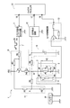
以下、本発明の実施の形態を、図面を参照しつつ説明する。図1は、ガスセンサ処理装置である酸素センサ制御装置1の概略構成を示す図である。酸素センサ制御装置1は、図示しないエンジンを備える車両(図示しない)に搭載され、酸素センサ2と共に用いて、これを制御し、エンジンの排気ガス中の酸素濃度を検出する。
Hereinafter, embodiments of the present invention will be described with reference to the drawings. FIG. 1 is a diagram showing a schematic configuration of an oxygen sensor control device 1 which is a gas sensor processing device. The oxygen sensor control device 1 is mounted on a vehicle (not shown) including an engine (not shown), and is used together with the
この酸素センサ2は、ジルコニアを主体とした酸素イオン伝導体である固体電解質体に一対の電極3P,3Nを形成した検出素子3と、この検出素子3を加熱するヒータ4を有している。より具体的には、有底筒状をなした固体電解質体からなる検出素子3の外周面に形成した一方の電極3Nは排気ガスに晒され、内周面に形成した他方の電極3Pは基準ガス(大気)に晒されている。そして、検出素子3の有底筒状の内部空間には、棒状のヒータ4を内挿されて酸素センサ2が構成されている。この固体電解質体からなる検出素子3は、活性化状態となる600℃を越える活性化温度に、ヒータ4で加熱されることで、良好な酸素イオン伝導性を示し、これにより、酸素濃度の検出が可能となっている。そして、酸素センサ2は、酸素センサ制御装置1により、検出素子3が活性化温度内の一定温度を維持するように、ヒータ4への通電が制御される。
The
ヒータ4は、タングステンあるいは白金を主体とした発熱抵抗体5と、この発熱抵抗体5に繋がる端子4P,4Nを有する。ヒータ4の一方の端子4Pは、バッテリ20の+極に接続されている。なお、このバッテリ20の−極は、車両のシャーシGNDである基準電位(以下、GNDという)に接続されている。さらに、ヒータ4のもう一方の端子4Nは、ヒータ制御回路13のうち、図示しない電流制限抵抗を介して、スイッチング素子であるNPN型のトランジスタTr1のコレクタ出力に接続されている。また、トランジスタTr1のエミッタは、GNDに接続されており、ベースは、マイクロプロセッサ10のPWM出力ポート18に接続されている。そして、ヒータ4は、このヒータ制御回路13によって、PWM制御による通電が行われ、これにより、検出素子3が加熱される。また、検出素子3を活性化温度内の一定温度に維持する際には、マイクロプロセッサ10によるPID制御またはPI制御で、PWM制御のデューティ比が決定される。なお、ヒータ制御回路13を構成するスイッチング素子は、トランジスタTr1に限らず、FET等を用いて構成しても良い。なお、バッテリ20からは、図示しない電源回路により、酸素センサ制御装置1で用いる+5V電源やマイクロプロセッサ10のVCC電源(図示しない)が生成されている。
The
検出素子3は、内部抵抗Riを有しており、その抵抗値は、固体電解質体の温度上昇に応じて低下する特性を有する。そして、この内部抵抗Riと検出素子3の素子温度との間には、所定の相関関係があることが知られており、内部抵抗Riが目標抵抗値となるように制御することにより、素子温度を所定の温度に維持することが可能である。 The detection element 3 has an internal resistance Ri, and the resistance value has a characteristic of decreasing as the temperature of the solid electrolyte body increases. It is known that there is a predetermined correlation between the internal resistance Ri and the element temperature of the detection element 3, and the element temperature is controlled by controlling the internal resistance Ri to be a target resistance value. Can be maintained at a predetermined temperature.
また、固体電解質体からなる検出素子3は、概略400℃以上で、酸素イオン伝導性を示し、電極3Nと電極3Pとの間の酸素濃度の違いにより、酸素濃淡電池となって、酸素濃度差に応じた起電力EVを発生する。このため、検出素子3の等価回路は、図1に示すように、電極3P,3N間に、起電力EVを発生する電池(酸素濃淡電池)と内部インピーダンスとが直列接続された回路を有していると見なすことができる。なお、内部インピーダンスは、純抵抗の内部抵抗Riのみならず、これに内部容量Ciが並列接続されていると見なすことができる。
In addition, the detection element 3 made of a solid electrolyte body exhibits oxygen ion conductivity at approximately 400 ° C. or higher, and becomes an oxygen concentration cell due to the difference in oxygen concentration between the
ところで、前述の通り、検出素子3を構成する固体電解質体は、固体電解質体の温度上昇に応じて内部抵抗Riが低下する特性を有するが、非活性時のうち、固体電解質体の温度が低いときは、内部抵抗Riが高く、検出素子3の電極3P,3N間は、ほぼ絶縁状態となる。そして、固体電解質体の温度が上昇するに伴い内部抵抗Riは低下し、検出素子3が活性化した場合(活性時)には、内部抵抗Riは低い値を示す。また、固体電解質体の温度上昇に伴って、検出素子3が、電極3P,3N間に酸素濃度差に応じた起電力EVを示すようになる。活性時における起電力EVは、素子温度により異なるが、具体的には、排気ガスの空燃比がリッチ側にある場合には約900mV前後を示し、リーン側にある場合には約50mV前後を示す。そして、リッチ側とリーン側の間の理論空燃比となるλ=1付近を境に、起電力EVは、急峻に変化する。
Incidentally, as described above, the solid electrolyte body constituting the detection element 3 has a characteristic that the internal resistance Ri decreases as the temperature of the solid electrolyte body increases, but the temperature of the solid electrolyte body is low during inactive time. When the internal resistance Ri is high, the
酸素センサ制御装置1(図1参照)の説明に戻る。抵抗器R1と抵抗器R2との直列回路で構成されて、+5V電源をこの抵抗器R1と抵抗器R2とで分圧するバイアス回路14は、本実施形態では、具体的には、R1=100kΩ,R2=10kΩとされており、+5V電源を抵抗器R1と抵抗器R2とで分圧したP点の電位が約450mVとなるように設定されている。このP点の電位は、上述した、リッチ側の約900mVとリーン側の約50mVのおおよそ中間の電圧値となるように選択したものである。そして、このP点の電位が、電流制限抵抗である抵抗器R3(具体的には、R3=10kΩ)を介して、Q点で、検出素子3の電極3Pに接続されている。また、検出素子3のもう一方の電極3Nは、GNDに接続されている。
Returning to the description of the oxygen sensor control device 1 (see FIG. 1). The
さらにQ点は、抵抗器R4(具体的には、R4=8.25kΩ)及びスイッチング素子であるPNP型のトランジスタTr2を介して、+5V電源に接続されている。なお、スイッチング素子は、トランジスタTr2に限らず、FET等を用いても良い。一方、Q点は、抵抗器R5とコンデンサC1からなるノイズ除去用のローパスフィルタ回路15(具体的には、R5=10kΩ,C1=0.033μF)にも接続されており、このローパスフィルタ回路15の出力であるS点が、出力検出回路12に接続されている。出力検出回路12は、図示しないサンプルホールド回路を内蔵し、その出力がマイクロプロセッサ10のA/D入力ポート17に接続されている。
Further, the point Q is connected to a + 5V power source via a resistor R4 (specifically, R4 = 8.25 kΩ) and a PNP transistor Tr2 which is a switching element. The switching element is not limited to the transistor Tr2, and an FET or the like may be used. On the other hand, the point Q is also connected to a low-
また、上述のトランジスタTr2は、エミッタが+5Vに接続され、コレクタが抵抗器R4に接続されている。そして、トランジスタTr2のベースには、ベース−エミッタ間抵抗の抵抗器R7とベース入力抵抗の抵抗器R6が接続されており、これら抵抗器R6,R7、トランジスタTr2及び抵抗器R4で、電圧シフト回路19を構成している。また、この電圧シフト回路19のうち、抵抗器R6の一方端であるT点には、パルス信号出力回路11が接続されている。パルス信号出力回路11は、マイクロプロセッサ10のI/O出力ポート16に接続されており、このI/O出力ポート16の出力が、パルス信号出力回路11を通して、T点にパルス信号SPとして出力される。パルス信号SPは、通常は、電圧シフト回路19のトランジスタTr2をオフするため、トランジスタTr2のエミッタ電位と同じ+5Vとされており、トランジスタTr2をオンとする期間だけ一時的に0Vに下がって、再び+5Vに戻る負論理の矩形状パルス電圧である。そして、このパルス信号SPを出力するパルス信号出力回路11と電圧シフト回路19により、後述する電圧シフトが行われる。
The transistor Tr2 has an emitter connected to + 5V and a collector connected to the resistor R4. The base of the transistor Tr2 is connected to a resistor R7 having a base-emitter resistance and a resistor R6 having a base input resistance. The resistors R6 and R7, the transistor Tr2 and the resistor R4 are connected to a voltage shift circuit. 19 is constituted. Further, in the
なお、パルス信号出力回路11は、具体的には、マイクロプロセッサ10のI/O出力ポート16の出力を反転または非反転でバッファすると共に、出力電圧をマイクロプロセッサ10のVCC電源から+5Vにレベル変換するための回路がレベル変換用のバッファICやトランジスタなどで構成されている。本実施形態では、I/O出力ポート16の出力がLレベルのとき、パルス信号出力回路11の出力のT点が+5Vとなり、I/O出力ポート16の出力がHレベルのとき、パルス信号出力回路11の出力のT点が0Vとなる反転型のバッファ回路とされている。
Specifically, the pulse
これらの回路の動作について、まず、電圧シフト回路19のトランジスタTr2がオフの場合について考える。トランジスタTr2がオフのときは、抵抗器R4には電流が流れない。そして、検出素子3は、非活性時のうち、固体電解質体の温度が低いときには、起電力EVが発生しない(EV=0V)。また、その内部抵抗Riは、絶縁状態に近く、抵抗器R2の10kΩよりも十分に大きい。このため、検出素子3には電流が流れず、電流制限抵抗R3にも電流が流れないので、固体電解質体の温度が低いときには、P点の電位は、抵抗器R1と抵抗器R2との分圧による約450mVとなる。そして、Q点及びS点もP点と同電位となり、出力検出回路12には、約450mVが入力される。一方、固体電解質体の温度が十分高くなった活性時には、例えば、検出素子3の素子温度が約700℃のときには、検出素子3の内部抵抗Riは、100Ω以下となり、抵抗器R2や抵抗器R3に比べて十分に小さい値となる。この活性時においては、検出素子3に起電力EVも発生する(リッチ側で約900mV前後、リーン側で約50mV前後)が、内部抵抗Riが上述のように十分に小さいので、Q点の電位は、抵抗器R2や抵抗器R3を流れる電流にほとんど影響を受けず、ほぼ起電力EVが示す値となる。そして、このQ点の電位が、ローパスフィルタ回路15を通して、S点で出力検出回路12に入力されており、出力検出回路12で検出素子3の起電力EVを検出することが可能となっている。
Regarding the operation of these circuits, first, consider the case where the transistor Tr2 of the
次に、電圧シフト回路19のトランジスタTr2がオンの場合について考える。トランジスタTr2がオフしている間は、前述の通り、抵抗器R4に電流が流れない。一方、トランジスタTr2がオンすると、抵抗器R4に電流Iが流れる。そして、検出素子3が活性時においては、検出素子3の内部抵抗Riは、抵抗器R3や抵抗器R2に比べて十分に小さいので、電流Iのほとんどは、検出素子3に流れる。従って、次述する内部容量Ciに流れる電流が収束してほとんど無くなった状態では、電流Iの大きさは、+5Vから検出素子3の起電力EVとトランジスタTr2のエミッタ−コレクタ間電圧(≒0V)を引いた値を、抵抗器R4と検出素子3の内部抵抗Riとの和(直列合成抵抗)で除した値となる(I≒(5−EV)/(R4+Ri))。トランジスタTr2がオフの間もオンの間も、電極3P,3N間の酸素濃度差に変化がなく、起電力EVが一定であるとすると、トランジスタTr2がオンの間の検出素子電圧VEは、オフの間の検出素子電圧VEに対して、内部抵抗Riに生じる電圧降下Ri×Iだけ上乗せさることとなる。即ち、トランジスタTr2がオンすることにより、検出素子電圧VEが、オフの時点でのシフト前電圧VE1(=EV)からシフト後電圧VE2(=EV+Ri×I)までシフトされる、電圧シフトを生じさせることができる。
Next, consider the case where the transistor Tr2 of the
これによって生じる、シフト後電圧VE2とシフト前電圧VE1との差分(VE2−VE1)をシフト電圧VSとする。すると、シフト前電圧VE1は、トランジスタTr2がオフのため、検出素子3の発生する起電力EVとなるので、シフト電圧VSは、内部抵抗Riに電流が流れることによって生じる電圧降下に相当する内部抵抗分電圧Viとなる。この内部抵抗分電圧Viは、Vi=Ri×(5−EV)/(R4+Ri)として与えられる。従って、出力検出回路12で、シフト前電圧VE1(=EV)及びシフト後電圧VE2(=VE1+VS=EV+Vi)をそれぞれ検知することで、シフト電圧VS、即ち、内部抵抗分電圧Viの大きさが分かる。またさらに、抵抗器R4の大きさとの比から、内部抵抗Riの大きさを求めることができる。
A difference (VE2−VE1) between the post-shift voltage VE2 and the pre-shift voltage VE1 generated thereby is defined as a shift voltage VS. Then, since the pre-shift voltage VE1 is an electromotive force EV generated by the detection element 3 because the transistor Tr2 is off, the shift voltage VS is an internal resistance corresponding to a voltage drop caused by a current flowing through the internal resistance Ri. Divided voltage Vi. This internal resistance divided voltage Vi is given as Vi = Ri × (5-EV) / (R4 + Ri). Therefore, by detecting the pre-shift voltage VE1 (= EV) and the post-shift voltage VE2 (= VE1 + VS = EV + Vi) by the
ところで、トランジスタTr2をオンして、シフト前電圧VE1からシフト後電圧VE2への電圧シフトを行っている期間を電圧シフト期間TSとする(図2参照)と、この電圧シフト期間TSには、内部抵抗Riに電流が流れると共に、検出素子3がなす内部容量Ciに、時定数Ci・Riに従って、電荷が蓄積される。
一方、その後トランジスタTr2をオフさせて、電圧シフト期間TSを終了させる。すると、検出素子3(その電極3P,3N間)には、外部から電流が流れ込まなくなると共に、外部電圧が印加されなくなる。すると、内部容量Ciに蓄積された電荷が、内部抵抗Riを通じて自己放電される。これにより、検出素子電圧VEは、回復期間TKに亘り、おおむね検出素子3の内部抵抗Ri及び内部容量Ciで決定される時定数によって指数関数的に減衰して、シフト後電圧VE2からシフト前電圧VE1に戻る電圧変化を生じる。
By the way, when the transistor Tr2 is turned on and a period during which the voltage shift from the pre-shift voltage VE1 to the post-shift voltage VE2 is performed is referred to as a voltage shift period TS (see FIG. 2), A current flows through the resistor Ri and charges are accumulated in the internal capacitance Ci formed by the detection element 3 according to the time constant Ci · Ri.
On the other hand, after that, the transistor Tr2 is turned off to end the voltage shift period TS. Then, no current flows into the detection element 3 (between its
ところで、検出素子3が劣化すると、検出素子3の素子インピーダンスが増加傾向となって、同一温度における検出素子の内部抵抗Riが増加すると共に、内部容量Ciも変化する。このため、劣化の進行程度により、上述の指数関数的な電圧変化のしかた(傾向)に差(違い)が生じる。また、この電圧変化は、外乱の影響を受け難く、検出素子3の素子インピーダンス(内部抵抗Ri及び内部容量Ci)によりほぼ定まる。従って、この電圧変化に基づいて、検出素子3の劣化の程度を示す劣化指標ID(後述する)を検知することができる。 By the way, when the detection element 3 deteriorates, the element impedance of the detection element 3 tends to increase, the internal resistance Ri of the detection element at the same temperature increases, and the internal capacitance Ci also changes. For this reason, a difference (difference) occurs in the above-described exponential voltage change method (trend) depending on the degree of progress of deterioration. Further, this voltage change is hardly affected by disturbance and is substantially determined by the element impedance (internal resistance Ri and internal capacitance Ci) of the detection element 3. Therefore, based on this voltage change, it is possible to detect a deterioration index ID (described later) indicating the degree of deterioration of the detection element 3.
なお、前述の通り、酸素濃度(特定ガスのガス濃度)を検出する際には、検出素子3を酸素濃淡電池として十分機能させるため、600℃を越える活性化温度(例えば、上述の約700℃)にまで素子温度を上げて使用する。検出素子3の素子温度が約700℃のときは、検出素子3の内部抵抗Riは、100Ω以下の小さな値となる。しかるに、本実施形態では、抵抗器R4は、これより遥かに大きいR4=8.25kΩであるので、トランジスタTr2をオンした場合に、内部抵抗Riによって生じる内部抵抗分電圧Vi(シフト電圧VS)も小さな値となる。このため、回復期間TKに生じる電圧変化も小さく、上述の劣化指標IDを精度良く検知しにくい。 As described above, when detecting the oxygen concentration (the gas concentration of the specific gas), an activation temperature exceeding 600 ° C. (for example, the above-described about 700 ° C.) is used in order to make the detection element 3 function sufficiently as an oxygen concentration cell. The device temperature is increased to When the element temperature of the detection element 3 is about 700 ° C., the internal resistance Ri of the detection element 3 is a small value of 100Ω or less. However, in the present embodiment, the resistor R4 is much larger than R4 = 8.25 kΩ, so that when the transistor Tr2 is turned on, the internal resistance divided voltage Vi (shift voltage VS) generated by the internal resistance Ri is also obtained. Small value. For this reason, the voltage change which arises in the recovery period TK is also small, and it is difficult to detect the above-described deterioration index ID with high accuracy.
しかしながら、酸素濃度の検出時には、検出素子3の素子温度を高く(例えば700℃)保つ必要があるが、劣化指標IDを検知する場合は、素子温度をこれほど高く保つ必要は無い。検出素子3を構成する固体電解質体は、400℃程度で酸素イオン伝導性を示しはじめる。また、同時に検出素子3の内部抵抗Riも、絶縁状態に比べて十分低い値を示す一方、上述の活性化状態(例えば700℃)に比して十分高い値となる。例えば、本実施形態では、素子温度が400℃のときの検出素子3の内部抵抗Riは、約2560Ωとなり、700℃の場合の数10倍の大きさとなり、抵抗器R4の1/3程度の大きさとなる。従って、この状態で、劣化指標IDを検知すれば、内部抵抗Riに比例するシフト電圧VSも大きくでき、回復期間TKに生じる電圧変化も大きくできる。
However, when detecting the oxygen concentration, it is necessary to keep the element temperature of the detection element 3 high (for example, 700 ° C.), but when detecting the deterioration index ID, it is not necessary to keep the element temperature so high. The solid electrolyte body constituting the detection element 3 starts to exhibit oxygen ion conductivity at about 400 ° C. At the same time, the internal resistance Ri of the detection element 3 also shows a sufficiently low value compared to the insulation state, but also a sufficiently high value compared to the above-described activated state (for example, 700 ° C.). For example, in this embodiment, the internal resistance Ri of the detection element 3 when the element temperature is 400 ° C. is about 2560Ω, which is several ten times as large as that at 700 ° C., which is about 1/3 of the
そこで、劣化指標IDを検知するに当たり、本実施形態では、検出素子の内部抵抗Riが、特定ガスのガス濃度を検出する際(特定ガスのガス濃度を検出可能な期間)の内部抵抗Ri(第1内部抵抗Ri1)よりも大きい状態で検知する。具体的には、素子温度が約400℃で、内部抵抗Riが2560Ωのときに劣化指標IDを検知するようにする。更に具体的には、車両の運転を終了し(従って、検出素子3が活性化状態とされる酸素センサ2による酸素濃度の検知を終了し)、エンジンの停止と共に、酸素センサ2のヒータ4への通電を停止し、10分間の待ち時間を設けて、検出素子3が冷却するのを待つ。その後、内部抵抗Riが2560Ωとなるように目標抵抗値を定めて、ヒータ4の通電制御を再度行い、内部抵抗Riを2560Ωとしてから、劣化指標IDを検知する。
Therefore, in detecting the deterioration index ID, in this embodiment, the internal resistance Ri (the period in which the gas concentration of the specific gas can be detected) is detected when the internal resistance Ri of the detection element detects the gas concentration of the specific gas. 1 is detected in a state larger than the internal resistance Ri1). Specifically, the degradation index ID is detected when the element temperature is about 400 ° C. and the internal resistance Ri is 2560Ω. More specifically, the operation of the vehicle is terminated (therefore, the detection of the oxygen concentration by the
図2に、本実施形態の酸素センサ制御装置1により、劣化指標IDを検知するにあたり、検出素子3について電圧シフトをさせたときの、電圧シフト期間TS及び回復期間TKにおける、検出素子電圧VEの変化波形を示す。なお、劣化指標IDの検知にあたり、検出素子3の内部抵抗Riが2560Ωとなるように、ヒータ4を通電制御している。
この図2においては、電圧をシフトさせる以前(時刻t=0以前)には、電圧シフト回路19のトランジスタTr2がオフとされており、検出素子電圧VEは、1.02Vになっている。この検出素子電圧VEは、素子温度約400℃のときの検出素子3の起電力EVを示している。これをシフト前電圧VE1(=EV)とする。
FIG. 2 shows the detection element voltage VE in the voltage shift period TS and the recovery period TK when a voltage shift is performed on the detection element 3 when the deterioration index ID is detected by the oxygen sensor control device 1 of the present embodiment. A change waveform is shown. In detecting the deterioration index ID, the
In FIG. 2, before the voltage is shifted (before time t = 0), the transistor Tr2 of the
その後、時刻t=0で、電圧シフト回路19のトランジスタTr2をオンさせ、電圧シフトを開始する(電圧シフト期間TSの開始)と、検出素子3に電流が流れて、検出素子3の内部抵抗Riに電圧降下を生じると共に、内部容量Ciに電荷を蓄積しつつ、検出素子電圧VEが立ち上がる。本実施形態では、電圧シフト期間TSは3msecとした。この電圧シフト期間TSのうち、その終期(終了時)である第1検知タイミングt1(時刻t=t1)には、検出素子電圧VEは、ほぼ平衡状態に近づいて、シフト後電圧VE2となる。そこで、この第1検知タイミングt1で、検出素子電圧VEを検知して、これを第1電圧V1(=シフト後電圧VE2)とする。
After that, at time t = 0, when the transistor Tr2 of the
内部抵抗Riが一定値(本実施形態では、Ri=2560Ω)となるように制御されている条件の下で、電圧シフト期間TS(本実施形態では3msec)を時定数Ci・Riよりも十分長くすれば(例えば、3倍以上)、シフト後電圧VE2(第1電圧V1)は、内部抵抗Riで定まる値に収束し、劣化の程度によらず、ほぼ同じ値となる。また、時刻t=t1では、シフト後電圧VE2とシフト前電圧VE1との差分(VE2−VE1)であるシフト電圧VSが、内部抵抗Riによって生じる内部抵抗分電圧Viとなり、シフト後電圧VE2=起電力EV+内部抵抗分電圧Vi(シフト電圧VS)となる。 Under the condition that the internal resistance Ri is controlled to be a constant value (Ri = 2560Ω in this embodiment), the voltage shift period TS (3 msec in this embodiment) is sufficiently longer than the time constant Ci · Ri. Then (for example, three times or more), the post-shift voltage VE2 (first voltage V1) converges to a value determined by the internal resistance Ri, and becomes substantially the same value regardless of the degree of deterioration. At time t = t1, the shift voltage VS, which is the difference (VE2-VE1) between the post-shift voltage VE2 and the pre-shift voltage VE1, becomes the internal resistance divided voltage Vi generated by the internal resistance Ri, and the post-shift voltage VE2 = start Electric power EV + internal resistance divided voltage Vi (shift voltage VS).
トランジスタTr2をオフさせ、電圧シフト期間TSを終了させると、これに続いて、検出素子電圧VEを、シフト後電圧VE2からシフト前電圧VE1に戻す回復期間TKとなる。この回復期間TKには、トランジスタTr2がオフとなっているので、図1から容易に理解できるように、シフト電圧VSにより内部容量Ciに蓄積された電荷は、内部抵抗Riを通じて自己放電される。これにより、検出素子3の電極間3P,3Nには、おおむね検出素子3の内部抵抗Ri及び内部容量Ciで決定される時定数によって指数関数的に減衰して、シフト後電圧VE2からシフト前電圧VE1に戻る電圧変化を生じる(図2参照)。本実施形態では、この回復期間TKのうち、電圧シフト期間TSの終了から3msec後である第2検知タイミングt2(時刻t=t2)で、検出素子電圧VEを検知して、これを第2電圧V2とする。 When the transistor Tr2 is turned off and the voltage shift period TS is ended, a detection period TK in which the detection element voltage VE is returned from the post-shift voltage VE2 to the pre-shift voltage VE1 follows. Since the transistor Tr2 is off during the recovery period TK, the charge accumulated in the internal capacitor Ci by the shift voltage VS is self-discharged through the internal resistor Ri, as can be easily understood from FIG. As a result, the inter-electrodes 3P and 3N of the detection element 3 are attenuated exponentially by the time constant determined by the internal resistance Ri and the internal capacitance Ci of the detection element 3, and are shifted from the post-shift voltage VE2 to the pre-shift voltage. A voltage change returning to VE1 occurs (see FIG. 2). In the present embodiment, the detection element voltage VE is detected at the second detection timing t2 (time t = t2) 3 msec after the end of the voltage shift period TS in the recovery period TK, and this is detected as the second voltage. V2.
前述したように、検出素子3の内部抵抗Riが2560Ωとなるように制御されているので、シフト後電圧VE2(第1電圧V1)は、劣化の程度によらずほぼ同じ値となる。回復期間TKに生じる電圧変化は、劣化の程度により異なり、劣化が進行するほど電圧がゆっくり減衰して、第2電圧V2は大きな値となる。即ち、第1電圧V1と第2電圧V2との差である1−2電圧差V1−2(=V1−V2)は、劣化の程度により異なり、劣化が進行するほど小さな値となる。従って、検出素子3の劣化の程度を示す劣化指標IDとして、この1−2電圧差V1−2を用いることができる。 As described above, since the internal resistance Ri of the detection element 3 is controlled to be 2560Ω, the post-shift voltage VE2 (first voltage V1) has almost the same value regardless of the degree of deterioration. The voltage change that occurs in the recovery period TK varies depending on the degree of deterioration, and the voltage gradually attenuates as the deterioration progresses, and the second voltage V2 becomes a large value. That is, the 1-2 voltage difference V1-2 (= V1-V2), which is the difference between the first voltage V1 and the second voltage V2, differs depending on the degree of deterioration, and becomes a smaller value as the deterioration proceeds. Therefore, the 1-2 voltage difference V1-2 can be used as the deterioration index ID indicating the degree of deterioration of the detection element 3.
なお、本実施形態では、内部抵抗Riが2560Ω(素子温度は約400℃)のときの、劣化指標IDである1−2電圧差V1−2を検知するようにした。しかし、劣化指標ID(1−2電圧差V1−2)を検知する際の内部抵抗Riの値は、検出素子3の劣化の程度の違いが、劣化指標ID(1−2電圧差V1−2)の違いとして判別可能な範囲で、適宜決めれば良い。 In the present embodiment, the 1-2 voltage difference V1-2 that is the deterioration index ID when the internal resistance Ri is 2560Ω (element temperature is about 400 ° C.) is detected. However, the value of the internal resistance Ri when detecting the deterioration index ID (1-2 voltage difference V1-2) depends on the deterioration index ID (1-2 voltage difference V1-2). ) May be determined appropriately within a range that can be discriminated as a difference.
次いで、本実施形態に係る酸素センサ制御装置1の制御を、特にそのマイクロプロセッサ10の動作を中心に、図3のフローチャートを参照して説明する。
図3に示す制御プログラムは、マイクロプロセッサ10が実行するプログラムの1つとして、ヒータ4の通電制御のためのPWM出力ポート18の出力更新タイミング毎に(従って、一定周期毎に)繰り返し呼び出される。また、必要な初期設定は、このプログラムが呼び出される前に別途実行されており、I/O出力ポート16の出力はLレベルとされている。これにより、パルス信号出力回路11の出力のT点は+5Vとなっており、トランジスタTr2はオフしている。
Next, the control of the oxygen sensor control device 1 according to the present embodiment will be described with reference to the flowchart of FIG. 3, particularly focusing on the operation of the
The control program shown in FIG. 3 is called repeatedly as one of the programs executed by the
先ず、ステップS1では、エンジンが停止しているか否かを判断する。そして、エンジンが停止していない場合(No、即ち、エンジンの運転中)には、ステップS2に進む。これ以降は、酸素濃度を検出する際(酸素濃度を検出可能な期間)の検出素子3の内部抵抗Riである第1内部抵抗Ri1の検知、ヒータ通電制御のPWMデューティ出力及び酸素濃度検出を行う。先ず、ステップS2では、第1内部抵抗Ri1を検知する。 First, in step S1, it is determined whether or not the engine is stopped. If the engine is not stopped (No, that is, during operation of the engine), the process proceeds to step S2. Thereafter, detection of the first internal resistance Ri1, which is the internal resistance Ri of the detection element 3 when detecting the oxygen concentration (period in which the oxygen concentration can be detected), PWM duty output of heater energization control, and oxygen concentration detection are performed. . First, in step S2, the first internal resistance Ri1 is detected.
次いで、ステップS3では、先回のエンジン運転後に、後述する劣化検知処理ルーチンにより、劣化指標IDとして検知され、不揮発性メモリ(図示しない)に記憶されていた1−2電圧差V1−2(図6参照:ステップS1078)が読み出される。 Next, in step S3, after the previous engine operation, a 1-2 voltage difference V1-2 (FIG. 2) detected as a deterioration index ID and stored in a non-volatile memory (not shown) by a deterioration detection processing routine described later. 6: Step S1078) is read out.
次いで、ステップS4では、1−2電圧差V1−2(劣化指標ID)の値に応じて、目標抵抗値RTを補正して補正後目標抵抗値RThを得る。検出素子3の素子温度を700℃一定に制御するため、補正後目標抵抗値RThは、1−2電圧差V1−2の値が小さい(劣化が進行している)ほど、大きな値に補正される。これは、検出素子3の劣化が進行するほど、同一温度での第1内部抵抗Ri1が大きくなるためであり、素子温度を一定に制御するためには、この第1内部抵抗Ri1の増加に合わせて、補正後目標抵抗値RThを大きくする必要がある。 Next, in step S4, the target resistance value RT is corrected according to the value of the 1-2 voltage difference V1-2 (deterioration index ID) to obtain a corrected target resistance value RTh. In order to control the element temperature of the detection element 3 at a constant 700 ° C., the corrected target resistance value RTh is corrected to a larger value as the value of the 1-2 voltage difference V1-2 is smaller (deterioration progresses). The This is because as the deterioration of the detection element 3 progresses, the first internal resistance Ri1 at the same temperature increases, and in order to keep the element temperature constant, the first internal resistance Ri1 is increased. Therefore, it is necessary to increase the corrected target resistance value RTh.
次いで、ステップS5では、補正された補正後目標抵抗値RThと第1内部抵抗Ri1とを用いて、第1内部抵抗Ri1が補正後目標抵抗値RThとなるように、ヒータ4を通電制御する。具体的には、PID制御またはPI制御によりヒータ通電制御のPWMデューティ比を決定し、PWM出力ポート18からPWMパルスを出力する。これにより、ヒータ4は、PWM制御され、検出素子3の素子温度が、検出素子3の劣化の程度に拘わらず、700℃一定に制御される。
Next, in step S5, the
次いで、ステップS6では、酸素濃度検出タイミングであるか否かを判断する。本実施形態では、ステップS2〜ステップS5によるヒータ通電制御のPWMデューティ比の更新回数10回に対して、酸素濃度の検出を1回の割合で実行する。ステップS6では、このタイミングを判断する。酸素濃度検出タイミングではない場合(No)は、そのまま処理を終了する。また、酸素濃度検出タイミングの場合(Yes)は、ステップS7に進む。 Next, in step S6, it is determined whether it is the oxygen concentration detection timing. In the present embodiment, the detection of the oxygen concentration is executed at a rate of once for the number of times the PWM duty ratio is updated 10 times in the heater energization control in steps S2 to S5. In step S6, this timing is determined. If it is not the oxygen concentration detection timing (No), the processing is terminated as it is. In the case of the oxygen concentration detection timing (Yes), the process proceeds to step S7.
ステップS7では、第1内部抵抗Ri1が補正後目標抵抗値RThとなっているか否かを判断する。酸素濃度を検出する際には、検出素子3の素子温度が所定の活性化温度(本実施形態では700℃)となっている(従って、第1内部抵抗Riが補正後目標抵抗値RThとなっている)必要がある。よって、酸素濃度を検出する前に、ステップS7で、これを判断する。ステップS7で、第1内部抵抗Ri1が補正後目標抵抗値RThでない場合(No)は、そのまま処理を終了する。一方、第1内部抵抗Ri1が補正後目標抵抗値RThである場合(Yes)には、ステップS8に進む。そして、ステップS8で、酸素濃度を検出した後、処理を終了する。 In step S7, it is determined whether or not the first internal resistance Ri1 is the corrected target resistance value RTh. When the oxygen concentration is detected, the element temperature of the detection element 3 is a predetermined activation temperature (700 ° C. in the present embodiment) (therefore, the first internal resistance Ri becomes the corrected target resistance value RTh). There is a need. Therefore, before detecting the oxygen concentration, this is determined in step S7. If it is determined in step S7 that the first internal resistance Ri1 is not the corrected target resistance value RTh (No), the process ends. On the other hand, when the first internal resistance Ri1 is the corrected target resistance value RTh (Yes), the process proceeds to step S8. In step S8, after detecting the oxygen concentration, the process is terminated.
一方、ステップS1において、エンジンが停止している場合(Yes)には、ステップS9に進む。そして、ステップS9では、エンジン停止後、10分が経過したか否かを判断する。10分経過していない場合(No)には、ステップS13に進み、ヒータ通電制御のPWMデューティ比を0%として、PWM出力ポート18から出力した後に、処理を終了する。これにより、エンジン停止後10分間は、ヒータ4に通電されないため、検出素子3の素子温度は徐々に低下する。
On the other hand, when the engine is stopped in step S1 (Yes), the process proceeds to step S9. In step S9, it is determined whether 10 minutes have elapsed since the engine was stopped. If 10 minutes have not elapsed (No), the process proceeds to step S13, where the PWM duty ratio of the heater energization control is set to 0% and output from the
エンジン停止から10分が経過すると、ステップS9でYesとなり、ステップS10に進み、劣化検知処理ルーチンを実行する。この劣化検知処理ルーチン(ステップS10)の終了後は、ステップS11に進む。このステップS11で、後述する検知完了フラグ(図4参照:ステップS108)がオフの場合(即ち、劣化指標IDの検知が完了していない場合)には(No)、そのまま処理を終了する。一方、検知完了フラグがオンの場合(即ち、劣化指標IDの検知が完了している場合)には(Yes)、ステップS12に進み、ヒータ4の通電を完全に停止した後、処理を終了する。
そして、以上の一連の処理は、一定周期毎に再度プログラムが呼び出されて、ステップS1から実行される。ただし、エンジンが停止し、検知完了フラグがオンとなってこの処理を終了した後は、再びエンジンが始動するまで、このプログラムの呼び出しは停止される。
When 10 minutes have elapsed since the engine was stopped, the determination in step S9 is Yes, the process proceeds to step S10, and the deterioration detection processing routine is executed. After the end of this deterioration detection routine (step S10), the process proceeds to step S11. In step S11, when a detection completion flag (see FIG. 4: step S108), which will be described later, is off (that is, when the detection of the deterioration index ID is not completed) (No), the processing is ended as it is. On the other hand, when the detection completion flag is ON (that is, when the detection of the deterioration index ID is completed) (Yes), the process proceeds to step S12, and the process is ended after the energization of the
The series of processes described above is executed again from step S1 by calling the program again at regular intervals. However, after the engine is stopped and the detection completion flag is turned on to end this processing, the calling of this program is stopped until the engine is started again.
次いで、ステップS10で示した劣化検知処理ルーチンについて、図4のフローチャートを参照して説明する。
先ず、ステップS101では、後述する電圧シフトサブルーチンを実行する(詳細は後述する。)。この電圧シフトサブルーチンでは、検出素子電圧VEの電圧シフトを行うと共に、シフト前電圧VE1、シフト後電圧VE2及びシフト電圧VSを取得する。また、この電圧シフトサブルーチンの終了時点で、I/O出力ポート16の出力はHレベルとされ、パルス信号出力回路11の出力のT点は0Vとなって、トランジスタTr2はオンしている。
Next, the deterioration detection processing routine shown in step S10 will be described with reference to the flowchart of FIG.
First, in step S101, a voltage shift subroutine described later is executed (details will be described later). In this voltage shift subroutine, the detection element voltage VE is shifted, and the pre-shift voltage VE1, the post-shift voltage VE2, and the shift voltage VS are acquired. At the end of this voltage shift subroutine, the output of the I /
次いで、ステップS102に進み、I/O出力ポート16の出力をLレベルに戻す。すると、パルス信号出力回路11の出力のT点は+5Vとなり、トランジスタTr2はオフにされる。
In step S102, the output of the I /
次いで、ステップS103に進み、電圧シフトサブルーチン(ステップS101)で取得したシフト電圧VS(内部抵抗分電圧Vi)及びシフト前電圧VE1(起電力EV)を用いて内部抵抗Riを計算する。そして、続くステップS104では、得られた内部抵抗Riが目標の第2目標抵抗値RU(本実施形態では、RU=2560Ω)となるように、ヒータ4を通電制御する。具体的には、PID制御またはPI制御によりヒータ通電制御のPWMデューティ比を決定し、PWM出力ポート18からPWMパルスを出力する。これにより、ヒータ4は、PWM制御され、検出素子3の温度が、約400℃に制御される。
Next, the process proceeds to step S103, and the internal resistance Ri is calculated using the shift voltage VS (internal resistance divided voltage Vi) and the pre-shift voltage VE1 (electromotive force EV) acquired in the voltage shift subroutine (step S101). In subsequent step S104, the
次いで、ステップS105では、劣化指標検知タイミングであるか否かが判断される。そして、続くステップS106では、劣化指標IDを検知する前に、取得した内部抵抗Riが第2目標抵抗値RU(=2560Ω)であるか否かが判断される。本実施形態では、ステップS101〜ステップS104によるヒータ通電制御のPWMデューティ比の更新回数10回に対して、ステップS105の判断を1回の割合で実行する。劣化指標検知タイミングでない場合(No)は、そのままこの劣化検知処理ルーチンを終了する。また、劣化指標検知タイミングの場合(Yes)は、ステップS106に進んで、内部抵抗Riが第2目標抵抗値RUであるか否かを判断する。ステップS106で、内部抵抗Riが第2目標抵抗値RUでないと判断された場合(No)は、そのままこの劣化検知処理ルーチンを終了する。 Next, in step S105, it is determined whether or not it is a deterioration index detection timing. In the subsequent step S106, it is determined whether or not the acquired internal resistance Ri is the second target resistance value RU (= 2560Ω) before the deterioration index ID is detected. In the present embodiment, the determination in step S105 is executed at a rate of once for the PWM duty ratio update count of heater energization control in steps S101 to S104. When it is not the deterioration index detection timing (No), this deterioration detection processing routine is finished as it is. In the case of the degradation index detection timing (Yes), the process proceeds to step S106, and it is determined whether or not the internal resistance Ri is the second target resistance value RU. If it is determined in step S106 that the internal resistance Ri is not the second target resistance value RU (No), the deterioration detection processing routine is terminated as it is.
一方、ステップS106で、内部抵抗Riが第2目標抵抗値RUであると判断された場合(Yes)は、ステップS107に進み、劣化指標IDを検知する劣化指標検知サブルーチン(詳細は後述する。)を実行する。そして、その終了後、ステップS108で、劣化指標IDの検知が完了したことを示す検知完了フラグをオンして、この劣化検知処理ルーチンを終了する。 On the other hand, if it is determined in step S106 that the internal resistance Ri is the second target resistance value RU (Yes), the process proceeds to step S107, and a deterioration index detection subroutine for detecting a deterioration index ID (details will be described later). Execute. After that, in step S108, a detection completion flag indicating that the detection of the deterioration index ID is completed is turned on, and the deterioration detection processing routine is ended.
次いで、ステップS101の電圧シフトサブルーチンについて、図5のフローチャートを参照して説明する。この電圧シフトサブルーチンは、前述したように、電圧シフト回路19を用いて、検出素子電圧VEをシフトさせると共に、シフト前電圧VE1、シフト後電圧VE2及びシフト電圧VSを取得する。
Next, the voltage shift subroutine of step S101 will be described with reference to the flowchart of FIG. In this voltage shift subroutine, as described above, the
先ず、ステップS1011において、マイクロプロセッサ10は、A/D入力ポート17を通じて、出力検出回路12により、次述する電圧シフト前のS点の電位、従って、ローパスフィルタ回路15を介してQ点の電位(シフト前電圧VE1)を測定する。この際、I/O出力ポート16の出力はLレベルとされており、パルス信号出力回路11の出力のT点は+5Vに、トランジスタTr2はオフにされている。このため、抵抗器R4には電流が流れず、Q点(及びS点)の電位は、検出素子3自身の起電力EVを示す値となっている。従って、このステップS1011で測定するS点(Q点)の電位の値(シフト前電圧VE1)は、起電力EVの値となる(VE1=EV)。
First, in step S1011, the
次いで、ステップS1012に進み、I/O出力ポート16の出力をHレベルとする。すると、パルス信号出力回路11の出力のT点は0Vとなり、トランジスタTr2がオンする。なお、このタイミングは、図2における時刻t=0に該当する。更に引き続いて、ステップS1013に進み、3msecの時間を計時するタイマをスタートさせる。
トランジスタTr2がオンすると、抵抗器R4に電流Iが流れ、この電流Iが検出素子3に流れ込む。すると、この電流Iにより、内部抵抗Riに電圧降下を生じさせると共に、内部容量Ciに電荷が徐々に蓄積される。このため、Q点の電位は、起電力EVから開始し、内部容量Ciへの電荷蓄積の進行と共に上昇する。Q点の電位において、起電力EVに上乗せされる電圧分は、内部抵抗Ri及び内部容量Ciの端子間電圧である。
In step S1012, the output of the I /
When the transistor Tr2 is turned on, a current I flows through the resistor R4, and this current I flows into the detection element 3. Then, the current I causes a voltage drop in the internal resistance Ri, and charges are gradually accumulated in the internal capacitance Ci. For this reason, the potential at the point Q starts from the electromotive force EV and rises with the progress of charge accumulation in the internal capacitor Ci. A voltage component added to the electromotive force EV at the potential at the point Q is a voltage between terminals of the internal resistance Ri and the internal capacitance Ci.
続くステップS1014では、ステップS1013の3msecのタイマがタイムアップするのを待つ。即ち、タイマがタイムアップしていない間(No)は、ステップS1014を繰り返す。従って、この間、内部容量Ciへの電荷の蓄積が進み、Q点の電位は上昇すると共に、平衡状態に近づく。そして、3msec経過し、タイマがタイムアップする(Yes)と、ステップS1015に進む。 In the subsequent step S1014, the process waits for the 3 msec timer in step S1013 to expire. That is, while the timer is not up (No), step S1014 is repeated. Accordingly, during this time, the accumulation of charges in the internal capacitor Ci proceeds, the potential at the point Q rises and approaches an equilibrium state. When 3 msec elapses and the timer expires (Yes), the process proceeds to step S1015.
ステップS1015では、トランジスタTr2をオンしてから、3msec経過した第1検知タイミングt1(時刻t=t1=3msec,図2参照)で、再び、A/D入力ポート17を通じて出力検出回路12により、S点の電位(従って、ローパスフィルタ回路15を通じたQ点の電位)を測定する。Q点の電位は、時刻t=0の立ち上がり開始後、3msecの期間(電圧シフト期間TS)が経過する間に、概略平衡状態に達しており(図2参照)、このステップS1015で測定した、時刻t=t1の時点の値をシフト後電圧VE2とする。
In step S1015, at the first detection timing t1 (time t = t1 = 3 msec, see FIG. 2) after 3 msec has elapsed since the transistor Tr2 was turned on, the
次いで、ステップS1016に進み、シフト電圧VSを、既に取得したシフト後電圧VE2とシフト前電圧VE1との差分(VE2−VE1)として求めて、電圧シフトサブルーチンを終了する。 Next, the process proceeds to step S1016, where the shift voltage VS is obtained as a difference (VE2−VE1) between the acquired post-shift voltage VE2 and the pre-shift voltage VE1, and the voltage shift subroutine is terminated.
次いで、ステップS107の劣化指標検知サブルーチンについて、図6のフローチャートを参照して説明する。なお、この劣化指標検知サブルーチン(ステップS107)は、前述したように、ステップS106で、検出素子3の内部抵抗Riが、第2目標内部抵抗値RU(=2560Ω)に等しいと判断された場合(Yes)に、実行される。 Next, the deterioration index detection subroutine of step S107 will be described with reference to the flowchart of FIG. In the deterioration index detection subroutine (step S107), as described above, when it is determined in step S106 that the internal resistance Ri of the detection element 3 is equal to the second target internal resistance value RU (= 2560Ω) ( Yes).
先ず、ステップS1071では、劣化検知処理ルーチン(ステップS10)におけるステップS101と同じ電圧シフトサブルーチンを実行する。この電圧シフトサブルーチンの終了時点(ステップS1016の終了時点)で、I/O出力ポート16の出力はHレベルとされ、パルス信号出力回路11の出力のT点は0Vとなって、トランジスタTr2はオンしている。
First, in step S1071, the same voltage shift subroutine as in step S101 in the deterioration detection processing routine (step S10) is executed. At the end of this voltage shift subroutine (the end of step S1016), the output of the I /
次いで、ステップS1072に進み、I/O出力ポート16の出力をLレベルに戻す。すると、パルス信号出力回路11の出力のT点は+5Vとなり、トランジスタTr2はオフにされる。これにより、電圧シフト期間TSが終了し、これに引き続いて、回復期間TKが開始される。
In step S1072, the output of the I /
続くステップS1073では、電圧シフトサブルーチンのステップS1015(第1検知タイミングt1)で取得したシフト後電圧VE2を、第1電圧V1として取得(コピー)する(V1=VE2)。
次いで、ステップS1074に進み、3msecの計時を行うタイマをスタートさせる。
トランジスタTr2をオフさせたため、検出素子3に、+5V電源を通じて外部電圧は印加されず、電流も流れない。このため、検出素子3では、内部容量Ciに蓄積された電荷を、内部抵抗Riを通じて自己放電する。このため、Q点の電位は、おおむね内部抵抗Ri及び内部容量Ciで決定される時定数によって指数関数的に減衰して、シフト後電圧VE2からシフト前電圧VE1に戻る電圧変化を生じる。
In subsequent step S1073, the shifted voltage VE2 acquired in step S1015 (first detection timing t1) of the voltage shift subroutine is acquired (copied) as the first voltage V1 (V1 = VE2).
Next, the process proceeds to step S1074, and a timer for measuring time of 3 msec is started.
Since the transistor Tr2 is turned off, no external voltage is applied to the detection element 3 through the + 5V power supply, and no current flows. For this reason, the detection element 3 self-discharges the electric charge accumulated in the internal capacitor Ci through the internal resistor Ri. For this reason, the potential at the point Q is attenuated exponentially by the time constant determined by the internal resistance Ri and the internal capacitance Ci, and a voltage change that returns from the post-shift voltage VE2 to the pre-shift voltage VE1 occurs.
続くステップS1075では、ステップS1074のタイマがタイムアップするのを待つ。即ち、タイマがタイムアップしていない間(No)は、ステップS1075を繰り返す。そして、3msec経過し、タイマがタイムアップする(Yes)と、ステップS1076に進む。 In the subsequent step S1075, the process waits for the timer in step S1074 to expire. That is, while the timer is not up (No), step S1075 is repeated. When 3 msec elapses and the timer expires (Yes), the process proceeds to step S1076.
ステップS1076では、トランジスタTr2をオフしてから、3msec経過した第2検知タイミングt2(時刻t=t2=6msec,図2参照)で、A/D入力ポート17を通して出力検出回路12により、S点の電位(ローパスフィルタ回路15を通じて、Q点の電位)を測定する。このステップS1076で測定した、時刻t=t2の時点の値を第2電圧V2とする。
In step S1076, at the second detection timing t2 after 3 msec from turning off the transistor Tr2 (time t = t2 = 6 msec, see FIG. 2), the
次いで、ステップS1077に進み、劣化指標IDである1−2電圧差V1−2を、既に取得した第1電圧V1と第2電圧V2との差(V1−V2)として求める。
さらに、ステップS1078に進み、取得した1−2電圧差V1−2を、不揮発性メモリに保存して、この劣化指標検知サブルーチンを終了する。
Next, the process proceeds to step S1077, and the 1-2 voltage difference V1-2, which is the deterioration index ID, is obtained as the difference (V1-V2) between the already acquired first voltage V1 and second voltage V2.
In step S1078, the acquired 1-2 voltage difference V1-2 is stored in the nonvolatile memory, and the deterioration index detection subroutine is terminated.
なお、本実施形態において、パルス信号出力回路11、電圧シフト回路19、ローパスフィルタ回路15、出力検出回路12及びステップS101〜S103を実行しているマイクロプロセッサ10が、抵抗指標検知手段に相当し、ここで検知する内部抵抗Riが抵抗指標IRに相当する。また、パルス信号出力回路11、電圧シフト回路19及びステップS1071を実行しているマイクロプロセッサ10が、電圧シフト手段に相当する。さらに、パルス信号出力回路11、電圧シフト回路19及びステップS1072を実行しているマイクロプロセッサ10が、回復手段に相当する。
In the present embodiment, the pulse
ここで、抵抗指標検知手段と電圧シフト手段とは、電圧シフトに用いるパルス信号出力回路11及び電圧シフト回路19を兼用している。なお、本実施形態では、抵抗指標検知手段と電圧シフト手段とで、電圧シフトサブルーチン(ステップS101,S1071)を兼用し、抵抗指標検知手段で、電圧シフト手段の電圧シフト期間TSと同様に、3msec間の電圧シフトを行った。しかし、抵抗指標検知手段で抵抗指標IRを検知する際の電圧シフトの期間は、劣化指標IDを検知する際の、電圧シフト手段による電圧シフト期間TSと異なっていても良く、実行するサブルーチンは別々でも良い。また、電圧シフト手段で電圧シフト回路19のトランジスタTr2をオンにし、回復手段でこれをオフにしており、電圧シフト手段と回復手段は、同一の回路(パルス信号出力回路11及び電圧シフト回路19)を用いている。
Here, the resistance index detection unit and the voltage shift unit also serve as the pulse
また、ステップS106〜S107を実行しているマイクロプロセッサ10が、劣化指標検知手段に相当し、内部抵抗Riが第2目標抵抗値RU(=2560Ω)であるときに、劣化指標IDである1−2電圧差V1−2を検知する。また、第2目標抵抗値RU(=2560Ω)が検知許容値IPに相当する。
さらに、ステップS2を実行しているマイクロプロセッサ10が、第1内部抵抗検知手段に相当し、ステップS4を実行しているマイクロプロセッサ10が、目標抵抗値補正手段に相当する。
また、ヒータ制御回路13及びステップS5を実行しているマイクロプロセッサ10が、第1ヒータ通電制御手段に相当し、ヒータ制御回路13及びステップS104を実行しているマイクロプロセッサ10が、第2ヒータ通電制御手段に相当する。
Further, the
Furthermore, the
The
以上で説明したように、本実施形態の酸素センサ制御装置1では、検出素子電圧VEを、シフト前電圧VE1からシフト後電圧VE2までシフトさせる電圧シフト手段(図6参照:ステップS1071)と、電圧シフト手段による電圧シフト期間TSの終了に続いて、検出素子電圧VEを、検出素子3の内部抵抗Ri及び内部容量Ciによる自己放電により、シフト後電圧VE2からシフト前電圧VE1に戻す回復手段(図6参照:ステップS1072)とを備えている。そしてさらに、回復手段による回復期間TKに生じる検出素子電圧VEの電圧変化に基づいて、検出素子3の劣化指標ID(1−2電圧差V1−2)を検知する劣化指標検知手段(図4参照:ステップS107)を備えている。回復期間TKでは、検出素子3の電極3P,3N間には、おおむね検出素子3の内部抵抗Ri及び内部容量Ciで決定される時定数によって指数関数的に減衰して、シフト後電圧VE2からシフト前電圧VE1に向かって戻る電圧変化を生じる。さらに、検出素子3が劣化すると、検出素子3の素子インピーダンスが増加傾向となり、同一温度における内部抵抗Riが増加すると共に、内部容量Ciも変化する。このため、劣化の進行程度により、上述の指数関数的な電圧変化のしかたに差が生じる。また、この電圧変化の差は、外乱の影響を受け難く、検出素子3の素子インピーダンスによりほぼ定まる。従って、この電圧変化に基づいて、劣化指標を検知する本実施形態の酸素センサ制御装置1では、酸素センサ2の検出素子3の劣化の程度を適切に検知することができる。
As described above, in the oxygen sensor control device 1 of the present embodiment, the voltage shift means (see FIG. 6: step S1071) for shifting the detection element voltage VE from the pre-shift voltage VE1 to the post-shift voltage VE2, the voltage Following the end of the voltage shift period TS by the shift means, the recovery means for returning the detection element voltage VE from the post-shift voltage VE2 to the pre-shift voltage VE1 by self-discharge by the internal resistance Ri and internal capacitance Ci of the detection element 3 (FIG. 6: Step S1072). Further, a deterioration index detecting means for detecting the deterioration index ID (1-2 voltage difference V1-2) of the detection element 3 based on the voltage change of the detection element voltage VE generated during the recovery period TK by the recovery means (see FIG. 4). Step S107). In the recovery period TK, between the
さらに、本実施形態の酸素センサ制御装置1では、第1内部抵抗検知手段(図3参照:ステップS2)と第1ヒータ通電制御手段(ステップS5)に加えて、劣化指標検知手段により検知された劣化指標ID(1−2電圧差V1−2)に応じて、フィードバック制御の目標抵抗値RTを補正して補正後目標電圧値RThとする目標抵抗値補正手段(ステップS4)を備えている。これにより、検出素子3の劣化状態に応じて目標抵抗値RTを変化させて、ヒータ4への通電を適切にフィードバック制御できるので、素子温度を適切な活性化温度に保つことができる。加えて、素子温度の上昇による劣化の促進を防止することができる。
Furthermore, in the oxygen sensor control device 1 of the present embodiment, the deterioration index detection unit detects the first internal resistance detection unit (see FIG. 3: step S2) and the first heater energization control unit (step S5). In accordance with the degradation index ID (1-2 voltage difference V1-2), there is provided target resistance value correcting means (step S4) that corrects the target resistance value RT of the feedback control to obtain a corrected target voltage value RTh. Thereby, the target resistance value RT is changed according to the deterioration state of the detection element 3, and the current supply to the
さらに、本実施形態の酸素センサ制御装置1では、劣化指標ID(1−2電圧差V1−2)を検知するのに先立ち、内部抵抗Ri(抵抗指標IR)を検知する抵抗指標検知手段(図4参照:ステップS101〜S103)を備え、劣化指標検知手段(ステップS106〜S107)は、この内部抵抗Ri(抵抗指標IR)が第2目標抵抗値RU(=2560Ω:検知許容値IP)であるとき(ステップS106で判定)に劣化指標IDを検知する。これにより、劣化指標IDの検知にあたって、検知時の条件を揃えることができ、適切に劣化指標ID(1−2電圧差V1−2)を検知することができる。 Further, in the oxygen sensor control device 1 of the present embodiment, the resistance index detection means (FIG. 5) detects the internal resistance Ri (resistance index IR) prior to detecting the degradation index ID (1-2 voltage difference V1-2). 4 includes steps S101 to S103), and the deterioration index detection means (steps S106 to S107) has an internal resistance Ri (resistance index IR) of the second target resistance value RU (= 2560Ω: detection allowable value IP). Sometimes (determined in step S106), the deterioration index ID is detected. Thereby, in detecting the degradation index ID, the conditions at the time of detection can be made uniform, and the degradation index ID (1-2 voltage difference V1-2) can be appropriately detected.
さらに、本実施形態の酸素センサ制御装置1では、内部抵抗Ri(抵抗指標IR)が第2目標抵抗値RU(検知許容値IP)となるように、ヒータ4への通電をフィードバック制御する(第2ヒータ通電制御手段、図4参照:ステップS104)。これにより、内部抵抗Ri(抵抗指標IR)が第2目標抵抗値RU(検知許容値IP)となっているタイミングで、確実に劣化指標ID(1−2電圧差V1−2)を検知することができる。
Furthermore, in the oxygen sensor control device 1 of the present embodiment, the energization to the
さらに、本実施形態の酸素センサ制御装置1では、内部抵抗Ri(抵抗指標IR)が第2目標抵抗値RU(検知許容値IP)であるときに、電圧シフト期間TS内の第1検知タイミングt1(図5参照:ステップS1015)における第1電圧V1(=シフト後電圧VE2)及び電圧シフト期間TS終了後の回復期間TK内の第2検知タイミングt2(図6参照:ステップS1076)における第2電圧V2の2つの電圧を計測すれば良く、簡易に劣化指標IDとしての1−2電圧差V1−2を得ることができる。 Furthermore, in the oxygen sensor control device 1 of the present embodiment, the first detection timing t1 within the voltage shift period TS when the internal resistance Ri (resistance index IR) is the second target resistance value RU (detection allowable value IP). (See FIG. 5: Step S1015) The first voltage V1 (= shifted voltage VE2) and the second voltage at the second detection timing t2 (see FIG. 6: Step S1076) within the recovery period TK after the end of the voltage shift period TS. It is only necessary to measure the two voltages V2, and the 1-2 voltage difference V1-2 as the deterioration index ID can be easily obtained.
さらに、本実施形態の酸素センサ制御装置1では、抵抗指標検知手段(図4参照:ステップS101〜S103)は、電圧シフト手段(図6参照:ステップS1071)と同様に、検出素子電圧VEをシフト前電圧VE1からシフト後電圧VE2までシフトさせており(ステップS101)、これに用いるパルス信号出力回路11及び電圧シフト回路19を電圧シフト手段と兼用している。このため、抵抗指標検知手段と電圧シフト手段とで別々の回路を用意する必要がなく、安価且つコンパクトな処理装置とすることができる。
Further, in the oxygen sensor control device 1 of the present embodiment, the resistance index detection means (see FIG. 4: steps S101 to S103) shifts the detection element voltage VE in the same manner as the voltage shift means (see FIG. 6: step S1071). The voltage is shifted from the previous voltage VE1 to the post-shift voltage VE2 (step S101), and the pulse
さらに、本実施形態の酸素センサ制御装置1では、エンジン停止後10分以上が経過して、劣化指標ID(内部抵抗Ri)を検知しており、劣化指標検知手段は、検出素子3の内部抵抗Riが、特定ガスのガス濃度(酸素濃度)を検出する際の内部抵抗Riである第1内部抵抗Ri1(100Ω以下)よりも大きい期間(内部抵抗Ri=2560Ω)に、劣化指標IDを検知する。これにより、回復期間TKに生じる検出素子電圧VEの電圧変化が大きくなるので、劣化指標IDを適切に検知できる。 Furthermore, in the oxygen sensor control device 1 of the present embodiment, the deterioration index ID (internal resistance Ri) is detected after 10 minutes or more after the engine is stopped, and the deterioration index detection means is configured to detect the internal resistance of the detection element 3. The degradation index ID is detected during a period (internal resistance Ri = 2560Ω) where Ri is greater than the first internal resistance Ri1 (100Ω or less), which is the internal resistance Ri when detecting the gas concentration (oxygen concentration) of the specific gas. . Thereby, since the voltage change of the detection element voltage VE generated in the recovery period TK becomes large, the deterioration index ID can be detected appropriately.
以上において、本発明のガスセンサ処理装置を、本実施形態の酸素センサ2の酸素センサ制御装置1に即して説明したが、本発明は上記実施形態に限定されるものではなく、その要旨を逸脱しない範囲で、適宜変更して適用できることはいうまでもない。
例えば、本発明における「ガスセンサ」は、酸素濃度を検出する酸素センサに限られず、窒素酸化物(NOx)の濃度を検出するNOxセンサ、炭化水素の濃度を検出するHCセンサなどであっても良い。
また、本発明は、ヒータを有さないガスセンサの出力を処理するガスセンサ処理装置に適用しても良い。
また、本実施形態では、抵抗指標IRとして、内部抵抗Riを用いたが、内部抵抗分電圧Viに相当するシフト電圧VSを抵抗指標IRとして用いても良い。
また、本実施形態では、劣化指標IDとして、前述の1−2電圧差V1−2を取得し、これを用いて、目標抵抗値RTを補正した。しかし、劣化指標IDとしては、これに限らない。例えば、本実施形態では、1−2電圧差V1−2を得るに当たり、第2電圧V2として、時刻t2=3msecにおけるシフト後電圧VE2を用いた(V1=VE2)が、回復期間TK内の2つの所定のタイミング(例えば、図2における時刻t3=3.5msecと、t4=6.5msec)における検出素子電圧VE(VE3,VE4)をそれぞれ計測し、これらの差を、劣化指標IDとしても良い。また、回復期間TK内に検出素子3の電極3P,3N間に生じる検出素子電圧VEを逐次計測し、その変化曲線から、この曲線に近似する指数関数の時定数を取得して、これを劣化指標IDとすることもできる。
In the above, the gas sensor processing apparatus of the present invention has been described in accordance with the oxygen sensor control apparatus 1 of the
For example, the “gas sensor” in the present invention is not limited to the oxygen sensor that detects the oxygen concentration, but may be a NOx sensor that detects the concentration of nitrogen oxide (NOx), an HC sensor that detects the concentration of hydrocarbon, or the like. .
The present invention may also be applied to a gas sensor processing apparatus that processes the output of a gas sensor that does not have a heater.
In this embodiment, the internal resistance Ri is used as the resistance index IR. However, a shift voltage VS corresponding to the internal resistance divided voltage Vi may be used as the resistance index IR.
In the present embodiment, the above-described 1-2 voltage difference V1-2 is acquired as the deterioration index ID, and the target resistance value RT is corrected using this. However, the deterioration index ID is not limited to this. For example, in this embodiment, in obtaining the 1-2 voltage difference V1-2, the shifted voltage VE2 at time t2 = 3 msec is used as the second voltage V2 (V1 = VE2). Two detection element voltages VE (VE3, VE4) at two predetermined timings (for example, time t3 = 3.5 msec and t4 = 6.5 msec in FIG. 2) are measured, and the difference between them may be used as the deterioration index ID. . Further, the detection element voltage VE generated between the
また、本実施形態では、劣化指標IDを検知する際の内部抵抗Riを、検出素子温度が約400℃となったときに相当する第2目標抵抗値RU=2560Ωに等しくなったときとした。しかし、第2目標抵抗値RUは、劣化指標IDを適切に検知できる範囲で適宜選択すれば良い。
また、電圧シフト期間TSを3msec、第1検知タイミングt1から第2検知タイミングt2までの期間を3msecとしたが、これらの値も、劣化指標IDが適切に検知できる範囲で適宜選択すれば良い。
In the present embodiment, the internal resistance Ri when detecting the deterioration index ID is set to be equal to the second target resistance value RU = 2560Ω corresponding to the detection element temperature of about 400 ° C. However, the second target resistance value RU may be appropriately selected within a range in which the deterioration index ID can be appropriately detected.
In addition, the voltage shift period TS is set to 3 msec and the period from the first detection timing t1 to the second detection timing t2 is set to 3 msec. However, these values may be appropriately selected within a range in which the deterioration index ID can be appropriately detected.
1 酸素センサ制御装置(ガスセンサ処理装置)
2 酸素センサ(ガスセンサ)
3 検出素子
3P,3N 電極
4 ヒータ
EV (酸素濃淡電池の)起電力
Ri 内部抵抗
Ci 内部容量
10 マイクロプロセッサ
11 パルス信号出力回路(抵抗指標検知手段、電圧シフト手段、回復手段)
12 出力検出回路(抵抗指標検知手段)
13 ヒータ制御回路(第1ヒータ通電制御手段、第2ヒータ通電制御手段)
15 ローパスフィルタ回路(抵抗指標検知手段)
19 電圧シフト回路(抵抗指標検知手段、電圧シフト手段、回復手段)
20 バッテリ
VE 検出素子電圧
VE1 シフト前電圧
VE2 シフト後電圧
TS 電圧シフト期間
TK 回復期間
ID 劣化指標
Ri1 第1内部抵抗
RT 目標抵抗値
RTh 補正後目標抵抗値
RU 第2目標抵抗値(検知許容値)
IR 抵抗指標
t1 第1検知タイミング
t2 第2検知タイミング
V1 第1電圧
V2 第2電圧
V1−2 1−2電圧差(劣化指標)
S2 第1内部抵抗検知手段
S4 目標抵抗値補正手段
S5 第1ヒータ通電制御手段
S101〜S103 抵抗指標検知手段
S104 第2ヒータ通電制御手段
S106〜S107 劣化指標検知手段
S1071 電圧シフト手段
S1072 回復手段
1 Oxygen sensor control device (gas sensor processing device)
2 Oxygen sensor (gas sensor)
3
12 Output detection circuit (resistance index detection means)
13 Heater control circuit (first heater energization control means, second heater energization control means)
15 Low-pass filter circuit (resistance index detection means)
19 Voltage shift circuit (resistance index detection means, voltage shift means, recovery means)
20 battery VE detection element voltage VE1 pre-shift voltage VE2 post-shift voltage TS voltage shift period TK recovery period ID deterioration index Ri1 first internal resistance RT target resistance value RTh corrected target resistance value RU second target resistance value (detection allowable value)
IR resistance index t1 first detection timing t2 second detection timing V1 first voltage V2 second voltage V1-2 1-2 voltage difference (degradation index)
S2 First internal resistance detection means S4 Target resistance value correction means S5 First heater energization control means S101 to S103 Resistance index detection means S104 Second heater energization control means S106 to S107 Degradation index detection means S1071 Voltage shift means S1072 Recovery means
Claims (7)
上記検出素子の上記電極間に生じている検出素子電圧を、シフト前電圧から、これと異なるシフト後電圧までシフトさせる電圧シフト手段と、
上記電圧シフト手段による電圧シフト期間の終了に続いて、上記検出素子の内部抵抗及び内部容量による自己放電により、上記検出素子電圧を、上記シフト後電圧から上記シフト前電圧に戻す回復手段と、
上記回復手段による回復期間に生じる電圧変化に基づいて、上記検出素子の劣化の程度を示す劣化指標を検知する劣化指標検知手段と、を備える
ガスセンサ処理装置。 A gas sensor processing apparatus that includes an oxygen ion conductive solid electrolyte body mainly composed of zirconia, has a pair of electrodes, and has a detection element that detects a gas concentration of a specific gas.
Voltage shift means for shifting the detection element voltage generated between the electrodes of the detection element from a pre-shift voltage to a different post-shift voltage;
Recovery means for returning the detection element voltage from the post-shift voltage to the pre-shift voltage by self-discharge by the internal resistance and internal capacitance of the detection element following the end of the voltage shift period by the voltage shift means;
A gas sensor processing apparatus, comprising: a degradation index detection unit that detects a degradation index that indicates a degree of degradation of the detection element based on a voltage change that occurs during a recovery period of the recovery unit.
前記ガスセンサは、前記検出素子を加熱するヒータを有し、
前記ガス濃度を検出する際の上記検出素子の内部抵抗である第1内部抵抗を検知する第1内部抵抗検知手段と、
上記第1内部抵抗が目標抵抗値となるように、上記ヒータへの通電をフィードバック制御する第1ヒータ通電制御手段と、
前記劣化指標検知手段により検知された前記劣化指標に応じて、上記目標抵抗値を補正する目標抵抗値補正手段と、を備える
ガスセンサ処理装置。 The gas sensor processing device according to claim 1,
The gas sensor has a heater for heating the detection element,
First internal resistance detection means for detecting a first internal resistance that is an internal resistance of the detection element when detecting the gas concentration;
First heater energization control means for feedback-controlling energization to the heater so that the first internal resistance becomes a target resistance value;
A gas sensor processing apparatus comprising: target resistance value correcting means for correcting the target resistance value according to the deterioration index detected by the deterioration index detecting means.
前記劣化指標検知手段により、前記劣化指標を検知するのに先立ち、前記検出素子の内部抵抗、及び、上記内部抵抗によって生じる内部抵抗分電圧のいずれかである抵抗指標を検知する抵抗指標検知手段を備え、
前記劣化指標検知手段は、
上記抵抗指標が、予め定めた検知許容値であるときに、前記劣化指標を検知する
ガスセンサ処理装置。 The gas sensor processing device according to claim 1 or 2,
Prior to detecting the deterioration index by the deterioration index detection means, a resistance index detection means for detecting a resistance index that is one of the internal resistance of the detection element and the internal resistance voltage generated by the internal resistance. Prepared,
The deterioration index detecting means is
A gas sensor processing device that detects the deterioration index when the resistance index is a predetermined detection allowable value.
前記ガスセンサは、前記検出素子を加熱するヒータを有し、
前記抵抗指標検知手段により検知された前記抵抗指標が、前記検知許容値となるように、上記ヒータへの通電をフィードバック制御する第2ヒータ通電制御手段を備える
ガスセンサ処理装置。 The gas sensor processing device according to claim 3,
The gas sensor has a heater for heating the detection element,
A gas sensor processing apparatus comprising second heater energization control means for feedback-controlling energization of the heater so that the resistance index detected by the resistance index detection means becomes the detection allowable value.
前記劣化指標検知手段は、
前記劣化指標として、前記電圧シフト期間内の第1検知タイミングにおける前記検出素子電圧である第1電圧と、上記電圧シフト期間終了後の前記回復期間内の第2検知タイミングにおける上記検出素子電圧である第2電圧との差である1−2電圧差を検知する
ガスセンサ処理装置。 The gas sensor processing device according to claim 3 or 4, wherein:
The deterioration index detecting means is
As the deterioration index, the first voltage that is the detection element voltage at the first detection timing within the voltage shift period and the detection element voltage at the second detection timing within the recovery period after the end of the voltage shift period. The gas sensor processing apparatus which detects the 1-2 voltage difference which is a difference with a 2nd voltage.
前記抵抗指標検知手段と、
前記電圧シフト手段とは、
前記検出素子の前記検出素子電圧を、前記シフト前電圧から前記シフト後電圧までシフトさせる回路を兼用してなる
ガスセンサ処理装置。 The gas sensor processing device according to any one of claims 3 to 5,
The resistance index detection means;
The voltage shift means is
A gas sensor processing apparatus that also serves as a circuit that shifts the detection element voltage of the detection element from the pre-shift voltage to the post-shift voltage.
前記劣化指標検知手段は、
前記検出素子の内部抵抗が、前記ガス濃度を検出する際の上記内部抵抗である第1内部抵抗よりも大きい期間に、前記劣化指標を検知する
ガスセンサ処理装置。 It is a gas sensor processing apparatus as described in any one of Claims 1-6,
The deterioration index detecting means is
The gas sensor processing apparatus which detects the said degradation index in the period when the internal resistance of the said detection element is larger than the 1st internal resistance which is the said internal resistance at the time of detecting the said gas concentration.
Priority Applications (3)
| Application Number | Priority Date | Filing Date | Title |
|---|---|---|---|
| JP2012004568A JP5648001B2 (en) | 2012-01-13 | 2012-01-13 | Gas sensor processing equipment |
| EP13000122.5A EP2615284A3 (en) | 2012-01-13 | 2013-01-10 | Exhaust gas sensor deterioration detection |
| US13/739,543 US9068934B2 (en) | 2012-01-13 | 2013-01-11 | Gas sensor processing apparatus |
Applications Claiming Priority (1)
| Application Number | Priority Date | Filing Date | Title |
|---|---|---|---|
| JP2012004568A JP5648001B2 (en) | 2012-01-13 | 2012-01-13 | Gas sensor processing equipment |
Publications (2)
| Publication Number | Publication Date |
|---|---|
| JP2013142683A JP2013142683A (en) | 2013-07-22 |
| JP5648001B2 true JP5648001B2 (en) | 2015-01-07 |
Family
ID=47757263
Family Applications (1)
| Application Number | Title | Priority Date | Filing Date |
|---|---|---|---|
| JP2012004568A Active JP5648001B2 (en) | 2012-01-13 | 2012-01-13 | Gas sensor processing equipment |
Country Status (3)
| Country | Link |
|---|---|
| US (1) | US9068934B2 (en) |
| EP (1) | EP2615284A3 (en) |
| JP (1) | JP5648001B2 (en) |
Families Citing this family (10)
| Publication number | Priority date | Publication date | Assignee | Title |
|---|---|---|---|---|
| JP5904171B2 (en) * | 2013-08-09 | 2016-04-13 | 株式会社デンソー | Gas sensor control device |
| JP6343132B2 (en) * | 2013-08-30 | 2018-06-13 | 株式会社デンソーテン | Current control circuit and electronic control device |
| JP2015094331A (en) * | 2013-11-14 | 2015-05-18 | 日産自動車株式会社 | Device and method for determining deterioration of oxygen concentration sensor for internal combustion engine |
| US10443526B2 (en) * | 2016-09-14 | 2019-10-15 | Denso Corporation | Air-fuel ratio sensing device |
| JP6819238B2 (en) * | 2016-11-21 | 2021-01-27 | 株式会社デンソー | Wiring abnormality detection device |
| DE102017207802A1 (en) * | 2017-05-09 | 2018-11-15 | Robert Bosch Gmbh | Method for operating a sensor for detecting at least one property of a measuring gas in a measuring gas space |
| KR102074979B1 (en) * | 2018-11-20 | 2020-02-10 | 현대오트론 주식회사 | A Measurement method of internal resistance of oxygen sensor |
| JP7306338B2 (en) * | 2020-06-26 | 2023-07-11 | トヨタ自動車株式会社 | Air-fuel ratio sensor control system |
| WO2023181292A1 (en) * | 2022-03-24 | 2023-09-28 | 日立Astemo株式会社 | Air-fuel ratio control device |
| CN114720509B (en) * | 2022-06-08 | 2022-08-26 | 苏州芯镁信电子科技有限公司 | Gas detection assembly and preparation method thereof |
Family Cites Families (13)
| Publication number | Priority date | Publication date | Assignee | Title |
|---|---|---|---|---|
| JP3065127B2 (en) * | 1991-06-14 | 2000-07-12 | 本田技研工業株式会社 | Oxygen concentration detector |
| JP3003056B2 (en) * | 1991-06-27 | 2000-01-24 | 横河電機株式会社 | Self-diagnosis circuit |
| JP3692640B2 (en) * | 1996-02-28 | 2005-09-07 | 株式会社デンソー | Method for detecting element resistance of oxygen concentration sensor |
| US5852228A (en) * | 1996-07-10 | 1998-12-22 | Denso Corporation | Apparatus and method for controlling oxygen sensor heating |
| JPH1026599A (en) * | 1996-07-10 | 1998-01-27 | Denso Corp | Detecting apparatus for oxygen concentration |
| DE69720647T2 (en) * | 1996-11-06 | 2003-10-30 | Ngk Spark Plug Co | Method and device for determining the deterioration in the operation of a lambda probe with a large measuring range |
| JP3563941B2 (en) | 1996-11-06 | 2004-09-08 | 日本特殊陶業株式会社 | Method and apparatus for detecting state of deterioration of full-range air-fuel ratio sensor |
| JP3373741B2 (en) * | 1996-11-06 | 2003-02-04 | 株式会社フジクラ | Limit current type oxygen sensor device and sensor driving method |
| JP2004028676A (en) * | 2002-06-24 | 2004-01-29 | Teijin Ltd | Oxygen concentration measurement apparatus equipped with deterioration diagnosis function |
| JP4033072B2 (en) * | 2003-04-23 | 2008-01-16 | トヨタ自動車株式会社 | Control device for gas concentration sensor |
| JP4768796B2 (en) * | 2008-11-06 | 2011-09-07 | 日本特殊陶業株式会社 | Gas sensor control device and gas sensor control method |
| JP5481153B2 (en) * | 2009-10-14 | 2014-04-23 | 矢崎エナジーシステム株式会社 | Alarm |
| JP5170907B2 (en) * | 2010-01-11 | 2013-03-27 | 日本特殊陶業株式会社 | Control device for controlled parts for vehicles |
-
2012
- 2012-01-13 JP JP2012004568A patent/JP5648001B2/en active Active
-
2013
- 2013-01-10 EP EP13000122.5A patent/EP2615284A3/en active Pending
- 2013-01-11 US US13/739,543 patent/US9068934B2/en active Active
Also Published As
| Publication number | Publication date |
|---|---|
| JP2013142683A (en) | 2013-07-22 |
| US9068934B2 (en) | 2015-06-30 |
| EP2615284A3 (en) | 2018-04-18 |
| EP2615284A2 (en) | 2013-07-17 |
| US20130180853A1 (en) | 2013-07-18 |
Similar Documents
| Publication | Publication Date | Title |
|---|---|---|
| JP5648001B2 (en) | Gas sensor processing equipment | |
| JP5736197B2 (en) | Insulation state detection unit | |
| JP5348089B2 (en) | Sensor control device | |
| JP5964678B2 (en) | Oxygen sensor control device | |
| JP5492236B2 (en) | Oxygen sensor control device | |
| JP5851366B2 (en) | Sensor control device and sensor control system | |
| JP6112062B2 (en) | Air-fuel ratio sensor control device | |
| JP2006343306A (en) | Gas concentration detector | |
| JP4871776B2 (en) | Gas detection device and gas detection method | |
| JP6267866B2 (en) | Insulation state detector | |
| JP5848415B2 (en) | Temperature measuring device using negative temperature coefficient thermistor | |
| JP5519571B2 (en) | Gas sensor device and control method thereof | |
| JP6048442B2 (en) | Device impedance detector for oxygen concentration sensor | |
| US9714917B2 (en) | Method of controlling lambda sensor preheating and lambda sensor drive controller | |
| JP6379000B2 (en) | Gas sensor system | |
| JP2016105065A (en) | Oxygen concentration sensor control unit | |
| JP2010054230A (en) | Gas detector | |
| JP6063282B2 (en) | Insulation state detector | |
| JP2015194483A (en) | gas sensor control device | |
| JP5723321B2 (en) | Sensor output processing apparatus and sensor system | |
| JP2001228111A (en) | Element resistance detector for oxygen concentration sensor | |
| JP2010038869A (en) | Gas detector | |
| JP2013057593A (en) | Battery voltage monitoring device | |
| JP6255308B2 (en) | GAS SENSOR CONTROL SYSTEM, GAS SENSOR CONTROL DEVICE, AND GAS SENSOR CONTROL METHOD | |
| JP2011190786A (en) | Ion current detecting and processing device for internal combustion engine |
Legal Events
| Date | Code | Title | Description |
|---|---|---|---|
| A621 | Written request for application examination |
Free format text: JAPANESE INTERMEDIATE CODE: A621 Effective date: 20131118 |
|
| A977 | Report on retrieval |
Free format text: JAPANESE INTERMEDIATE CODE: A971007 Effective date: 20140306 |
|
| A131 | Notification of reasons for refusal |
Free format text: JAPANESE INTERMEDIATE CODE: A131 Effective date: 20140318 |
|
| A521 | Request for written amendment filed |
Free format text: JAPANESE INTERMEDIATE CODE: A523 Effective date: 20140508 |
|
| TRDD | Decision of grant or rejection written | ||
| A01 | Written decision to grant a patent or to grant a registration (utility model) |
Free format text: JAPANESE INTERMEDIATE CODE: A01 Effective date: 20141014 |
|
| A61 | First payment of annual fees (during grant procedure) |
Free format text: JAPANESE INTERMEDIATE CODE: A61 Effective date: 20141110 |
|
| R150 | Certificate of patent or registration of utility model |
Ref document number: 5648001 Country of ref document: JP Free format text: JAPANESE INTERMEDIATE CODE: R150 |
|
| R250 | Receipt of annual fees |
Free format text: JAPANESE INTERMEDIATE CODE: R250 |
|
| R250 | Receipt of annual fees |
Free format text: JAPANESE INTERMEDIATE CODE: R250 |
|
| R250 | Receipt of annual fees |
Free format text: JAPANESE INTERMEDIATE CODE: R250 |
|
| R250 | Receipt of annual fees |
Free format text: JAPANESE INTERMEDIATE CODE: R250 |
|
| R250 | Receipt of annual fees |
Free format text: JAPANESE INTERMEDIATE CODE: R250 |
|
| S531 | Written request for registration of change of domicile |
Free format text: JAPANESE INTERMEDIATE CODE: R313531 |
|
| R350 | Written notification of registration of transfer |
Free format text: JAPANESE INTERMEDIATE CODE: R350 |
|
| R250 | Receipt of annual fees |
Free format text: JAPANESE INTERMEDIATE CODE: R250 |
|
| R250 | Receipt of annual fees |
Free format text: JAPANESE INTERMEDIATE CODE: R250 |