JP5646644B2 - Distributed multi-core memory initialization - Google Patents
Distributed multi-core memory initialization Download PDFInfo
- Publication number
- JP5646644B2 JP5646644B2 JP2012541131A JP2012541131A JP5646644B2 JP 5646644 B2 JP5646644 B2 JP 5646644B2 JP 2012541131 A JP2012541131 A JP 2012541131A JP 2012541131 A JP2012541131 A JP 2012541131A JP 5646644 B2 JP5646644 B2 JP 5646644B2
- Authority
- JP
- Japan
- Prior art keywords
- memory
- processing nodes
- memory initialization
- subtask
- processing
- Prior art date
- Legal status (The legal status is an assumption and is not a legal conclusion. Google has not performed a legal analysis and makes no representation as to the accuracy of the status listed.)
- Active
Links
- 230000015654 memory Effects 0.000 title claims description 205
- 238000012545 processing Methods 0.000 claims description 166
- 238000000034 method Methods 0.000 claims description 25
- 230000008569 process Effects 0.000 claims description 11
- 230000009977 dual effect Effects 0.000 claims description 9
- 238000004891 communication Methods 0.000 claims description 5
- 238000012360 testing method Methods 0.000 description 20
- 238000010586 diagram Methods 0.000 description 7
- 238000004422 calculation algorithm Methods 0.000 description 6
- 230000006870 function Effects 0.000 description 6
- 230000008901 benefit Effects 0.000 description 4
- 230000001427 coherent effect Effects 0.000 description 4
- 230000002093 peripheral effect Effects 0.000 description 3
- 238000013459 approach Methods 0.000 description 2
- 238000004140 cleaning Methods 0.000 description 2
- 238000012937 correction Methods 0.000 description 2
- 230000001419 dependent effect Effects 0.000 description 2
- 230000004044 response Effects 0.000 description 2
- 238000012549 training Methods 0.000 description 2
- 238000012546 transfer Methods 0.000 description 2
- 230000005540 biological transmission Effects 0.000 description 1
- 230000015556 catabolic process Effects 0.000 description 1
- 238000004590 computer program Methods 0.000 description 1
- 238000013461 design Methods 0.000 description 1
- 238000011161 development Methods 0.000 description 1
- 238000005516 engineering process Methods 0.000 description 1
- 238000011423 initialization method Methods 0.000 description 1
- 230000007246 mechanism Effects 0.000 description 1
- 230000005055 memory storage Effects 0.000 description 1
- 238000012986 modification Methods 0.000 description 1
- 230000004048 modification Effects 0.000 description 1
- 230000000737 periodic effect Effects 0.000 description 1
- 230000006798 recombination Effects 0.000 description 1
- 238000005215 recombination Methods 0.000 description 1
- 238000013515 script Methods 0.000 description 1
- 238000006467 substitution reaction Methods 0.000 description 1
- 238000010998 test method Methods 0.000 description 1
- 238000011144 upstream manufacturing Methods 0.000 description 1
Images


Classifications
-
- G—PHYSICS
- G06—COMPUTING; CALCULATING OR COUNTING
- G06F—ELECTRIC DIGITAL DATA PROCESSING
- G06F9/00—Arrangements for program control, e.g. control units
- G06F9/06—Arrangements for program control, e.g. control units using stored programs, i.e. using an internal store of processing equipment to receive or retain programs
- G06F9/44—Arrangements for executing specific programs
- G06F9/4401—Bootstrapping
- G06F9/4405—Initialisation of multiprocessor systems
-
- G—PHYSICS
- G06—COMPUTING; CALCULATING OR COUNTING
- G06F—ELECTRIC DIGITAL DATA PROCESSING
- G06F15/00—Digital computers in general; Data processing equipment in general
- G06F15/16—Combinations of two or more digital computers each having at least an arithmetic unit, a program unit and a register, e.g. for a simultaneous processing of several programs
- G06F15/177—Initialisation or configuration control
-
- G—PHYSICS
- G06—COMPUTING; CALCULATING OR COUNTING
- G06F—ELECTRIC DIGITAL DATA PROCESSING
- G06F9/00—Arrangements for program control, e.g. control units
- G06F9/06—Arrangements for program control, e.g. control units using stored programs, i.e. using an internal store of processing equipment to receive or retain programs
- G06F9/44—Arrangements for executing specific programs
- G06F9/448—Execution paradigms, e.g. implementations of programming paradigms
- G06F9/4482—Procedural
- G06F9/4484—Executing subprograms
-
- G—PHYSICS
- G06—COMPUTING; CALCULATING OR COUNTING
- G06F—ELECTRIC DIGITAL DATA PROCESSING
- G06F9/00—Arrangements for program control, e.g. control units
- G06F9/06—Arrangements for program control, e.g. control units using stored programs, i.e. using an internal store of processing equipment to receive or retain programs
- G06F9/46—Multiprogramming arrangements
- G06F9/50—Allocation of resources, e.g. of the central processing unit [CPU]
- G06F9/5061—Partitioning or combining of resources
- G06F9/5066—Algorithms for mapping a plurality of inter-dependent sub-tasks onto a plurality of physical CPUs
Landscapes
- Engineering & Computer Science (AREA)
- Software Systems (AREA)
- Theoretical Computer Science (AREA)
- Physics & Mathematics (AREA)
- General Engineering & Computer Science (AREA)
- General Physics & Mathematics (AREA)
- Computer Security & Cryptography (AREA)
- Computer Hardware Design (AREA)
- Stored Programmes (AREA)
- Multi Processors (AREA)
Description
本発明は概してデータ処理システムに関する。1つの態様においては、本発明はシステムブート(system boot)に際してのメモリ初期化のための方法及び装置に関する。 The present invention generally relates to data processing systems. In one aspect, the present invention relates to a method and apparatus for memory initialization during system boot.
データ処理システム又はコンピューティングシステムは、独立したコンピューティング能力を1人以上のユーザに与えるように設計されており、例えばメインフレーム、ミニコンピュータ、ワークステーション、サーバ、パーソナルコンピュータ、インターネット端末、ノートブック、及び埋め込み型システムを含む多くの形態において見出すことができる。一般的にコンピュータシステムアーキテクチャは、選択されたシステムコンポーネント、関連するメモリ及び制御論理(典型的にはシステムボード上の)並びに入力及び/又は出力(I/O)をシステムに提供する複数の周辺デバイスへの高速高帯域幅(high speed, high bandwidth)のアクセスを1つ以上のマイクロプロセッサコアにもたらすことを含むように設計される。例えば図1は、従来のコンピュータシステム100のための例示的なアーキテクチャを示している。コンピュータシステム100は、「ノース(north)」ブリッジ104を介してシステムメモリ108に接続される1つ以上のプロセッサ102を含む。典型的には、メモリアレイ108は1つ以上のメモリモジュールを含み、またメモリモジュールの追加又は交換のためのメモリスロットを含むこともある。ノースブリッジ回路104は種々のメモリモジュールとインタフェースするようにプログラム可能であり、また図示されるように、ノースブリッジ回路104は複数のメモリモジュール108の間で共有される。その結果、異なる複数のメモリモジュールにデータ投入される(populated)場合、ノースブリッジ回路104は、各メモリモジュールが正確に動作することを可能にするパラメータでプログラムされる必要がある。図示されるノースブリッジ回路104は、高速高帯域幅バス(例えばメモリバス107)を介してメモリ108に接続され、また高速高帯域幅バス(例えばエーリンク(Alink)又はPCIバス)を介して「サウス(south)」ブリッジ112にも接続される。「サウス」ブリッジ112は、1つ以上のI/Oデバイス、例えば、周辺コンポーネント相互接続(Peripheral Component Interconnect)(PCI)バス110(PCIバス110は次いでネットワークインタフェースカード(NIC)120に接続される)、シリアルATアタッチメント(serial AT Attachment)(SATA)インタフェース114、ユニバーサルシリアルバス(USB)インタフェース116、及びローピンカウント(Low Pin Count)(LPC)バス118(LPCバス118は次いでスーパー入力/出力制御器チップ(SuperI/O)122及びBIOSメモリ124に接続される)に接続される。理解されるであろうように、他のバス、デバイス、及び/又はサブシステム、例えば、キャッシュ、モデム、並列又はシリアルのインタフェース、SCSIインタフェース等がコンピュータシステム100内に含まれ得ることが分かるはずである。また、ノースブリッジ104及びサウスブリッジ112は、単一チップ又は複数のチップで実装することができ、総称して「チップセット」と称される。代替的には、ブリッジチップの機能の全て又は一部はプロセッサ102内にある場合がある。
Data processing systems or computing systems are designed to provide independent computing capabilities to one or more users, such as mainframes, minicomputers, workstations, servers, personal computers, Internet terminals, notebooks, And can be found in many forms, including embedded systems. Generally, a computer system architecture includes a plurality of peripheral devices that provide a system with selected system components, associated memory and control logic (typically on a system board) and inputs and / or outputs (I / O). Designed to include providing high speed, high bandwidth access to one or more microprocessor cores. For example, FIG. 1 illustrates an exemplary architecture for a
コンピュータシステムは典型的には基本入力/出力システム(BIOS)と称される組み込み型ソフトウエアルーチンを含み、BIOSは、プログラマ又はユーザがシステムハードウエアとやりとりすることができるように、システムハードウエアとオペレーティングシステムの間でのソフトウエアインタフェースを提供する。BIOS命令は、不揮発性メモリ124(例えばROM(リードオンリメモリ)、PROM(プログラム可能なROM)、EPROM(消去可能なROM)、EEPROM(電気的に消去可能なROM)、フラッシュRAM(ランダムアクセスメモリ)等)内に記憶されており、そしてメモリを試験すること及び初期化すること、システムをインベントリすること(inventorying)及び初期化すること、並びにシステムを試験することを含む電源投入時の重要なコンピュータシステム機能を制御するために用いられる。電源投入時のこれらの機能は、「システムブート(system boot)」又は「システムをブートすること(booting the system)」と称され、システム電源投入のたびに又はシステムがリセットされるたびに生じ得る。図1に示される従来のコンピュータシステム100においては、BIOSは、コンピューティングシステム100をブートするために、ブートストラッププロセッサ(boot strap processor)と称されるプロセッサ102の1つ上で実行する。動作においてブートストラッププロセッサ102は、ノースブリッジ104を介してメモリアレイ108と通信する。ノースブリッジ回路104は、ダブルデータレート(DDR)バス等のメモリバス107とインタフェースする1つ以上のチャネル制御器に接続されるメモリ制御器(MC)106を含む。ノースブリッジ回路104はまた、標準的なバス109、例えば周辺コンポーネント相互接続(PCI)バス上で1つ以上のサウスブリッジ112とも通信する。サウスブリッジ112は1つ以上の入力/出力(I/O)デバイス120,122,124と通信するが、追加的な又はより少数のデバイス(図示せず)がサウスブリッジ112に接続されているかもしれない。
A computer system typically includes embedded software routines referred to as a basic input / output system (BIOS), which allows the programmer or user to interact with the system hardware. Provides a software interface between operating systems. The BIOS command is stored in a nonvolatile memory 124 (for example, ROM (read only memory), PROM (programmable ROM), EPROM (erasable ROM), EEPROM (electrically erasable ROM), flash RAM (random access memory). ) Etc.) and are important during power-up including testing and initializing the memory, inventorying and initializing the system, and testing the system. Used to control computer system functions. These functions at power-on are referred to as "system boot" or "booting the system" and can occur each time the system is powered on or the system is reset . In the
システム初期化に際して、ブートストラッププロセッサ102は、相当な時間を必要とし得るシステムブートの間に、全てのメモリ試験及びクリーニングを行う。大型サーバシステムは、多くの場合にブートするために数分を必要とし、その間、他のプロセッサはアイドルである。図示される例では、ブートストラッププロセッサ上で実行中のBIOSは、DDRメモリバス107上でのDIMMメモリ108からの情報に基づいてストラッププロセッサ102からレジスタをプログラムすることによって、ノースブリッジ回路104内のメモリ制御器106を初期化する。メモリ初期化は、メモリモジュールのデータ投入状況(population)を検証することと、メモリの適切な動作(スタックビット無し)を検証することと、メモリを既知の値に初期化し又はクリーニングすることと、を含み得る。大きなメモリ108(例えば8、16、又は32ギガバイトのメモリ)を伴う従来のシステムは、メモリを初期化するのに数分を必要とすることがあり、特に「DDRトレーニング」処理は、ブートストラッププロセッサ102を用いて、メモリ初期化タスク間の依存を問わずタスクの順序付けられたシーケンスを連続的に実行することによって、メモリを初期化する。この遅延は、大量のメモリ108が各制御器106に接続される場合に深刻である。
Upon system initialization, the
そこで、本願発明者によって発見されてきた当該分野における種々の問題に対処する改良されたメモリ初期化デバイス、方法論、及びシステムに対する要求が存在し、ここで、従来の解決法及び技術の種々の限界及び不利益は、後述の図面及び詳細な説明を参照して本願の残りを精査した後に当業者にとって明らかになるはずであるが、背景技術欄のこの説明は、説明される主題が従来技術であるとの了解を意図するものではないことが理解されるべきである。 Thus, there is a need for improved memory initialization devices, methodologies, and systems that address various problems in the art that have been discovered by the present inventors, where various limitations of conventional solutions and techniques exist. And the disadvantages should become apparent to those skilled in the art after reviewing the remainder of the application with reference to the drawings and detailed description that follow, but this description in the Background section is based on prior art. It should be understood that it is not intended to be understood.
概して、本発明の実施形態は、先行するタスクに依存せずに順序不問で実行が達成され得るようにメモリ初期化タスクをコアに分散させることによって多重コアコンピュータシステム内でメモリを初期化するためのシステム、方法、及び装置を提供する。選択された実施形態においては、複数の処理ノード又はコア及び複数のシステムメモリコンポーネントを含むシステムが提供される。選択された実施形態においては、処理ノード又はコアの1つは、メモリ初期化タスクを多重CPUノード/コアによって処理される個々のサブタスクに分割するための制御ノード/コア機能を提供するように選択される。個々のサブタスクは、実行のための他の「スレーブ(slave)」コアに送られ又は分散させられる。各スレーブコアでは、単一又は複数のサブタスクを処理する資源をスレーブコアが有している場合に、サブタスクは実行のためにスケジューリングされる。結果として、所与のスレーブコアでの所与のサブタスクの実行の時間は、他のスレーブコアでの他のサブタスクの実行と重複してよいし又はしなくてもよい。その結果、スレーブコアは、サブタスクを並列に又はシリアルに実行することが可能である。サブタスクが処理された後に、それらは制御コアが元のタスクを完了するために再結合される。これにより、スレーブコアはサブタスクを並列に実行することができるので、同時タスク実行が可能になり、結果として全体の実行時間が減少すると共に最適な性能がもたらされる。 In general, embodiments of the present invention are for initializing memory within a multi-core computer system by distributing memory initialization tasks across the core so that execution can be accomplished in an unordered manner independent of preceding tasks. A system, method, and apparatus are provided. In selected embodiments, a system is provided that includes multiple processing nodes or cores and multiple system memory components. In selected embodiments, one of the processing nodes or cores is selected to provide a control node / core function to divide memory initialization tasks into individual subtasks processed by multiple CPU nodes / cores Is done. Individual subtasks are sent or distributed to other “slave” cores for execution. In each slave core, subtasks are scheduled for execution when the slave core has resources to process single or multiple subtasks. As a result, the time of execution of a given subtask on a given slave core may or may not overlap with the execution of other subtasks on other slave cores. As a result, the slave core can execute the subtasks in parallel or serially. After the subtasks are processed, they are recombined for the control core to complete the original task. This allows the slave core to execute subtasks in parallel, thereby enabling simultaneous task execution, resulting in reduced overall execution time and optimal performance.
本発明の種々の実施形態によると、メモリ初期化タスク等のブート処理タスクを複数の処理ノードに行わせるための方法が提供される。方法の例示的な実施形態においては、制御処理ノードは、ブート処理タスク(例えばメモリ初期化タスク)を複数のブート処理サブタスク(例えばメモリ初期化サブタスク)に分割し、次いで対応する処理ノードを各サブタスクが有するように、制御処理ノードを含んでいてよい複数の処理ノードの間でサブタスクを分散させる。サブタスクを分散させるのに先立ち、制御処理ノードは、複数の処理ノードの間の通信リンクを初期化する。サブタスク分散の例を提供すると、処理ノードの1つは、シリアルプレゼンスディテクト(serial presence detect)(SPD)値をDIMMメモリから読み出すメモリ初期化サブタスクを割り当てられる一方で、処理ノードの他の1つは、SPD値に依存しない複雑な初期化タスクを実行するメモリ初期化サブタスクを割り当てられる。各メモリ初期化サブタスクは、実行のためにスケジューリングされ、次いで対応する処理ノードで実行されてサブタスク結果を生成する。選択された実施形態においては、対応する処理ノードでメモリ初期化サブタスクを実行するために、ソフトウエアルーチンが用いられる。制御処理ノードは、対応する処理ノードでのメモリ初期化サブタスクの実行に関する状況報告(status reports)を受信し、そして複数の処理ノードからのサブタスク結果が次いで制御処理ノードで結合され、ここで、複数のメモリ初期化サブタスクは、複数の処理ノードで並列に又はシーケンスに実行されてよい。例えば、処理ノードの1つは、それが割り当てられたメモリ初期化サブタスクを、処理ノードの他の1つであってその対応するメモリ初期化サブタスクを実行する他の1つと並列に実行することができる。 According to various embodiments of the present invention, a method is provided for causing a plurality of processing nodes to perform a boot processing task, such as a memory initialization task. In an exemplary embodiment of the method, the control processing node divides a boot processing task (eg, memory initialization task) into a plurality of boot processing subtasks (eg, memory initialization subtask), and then assigns the corresponding processing node to each subtask. As such, the subtasks are distributed among a plurality of processing nodes that may include control processing nodes. Prior to distributing the subtasks, the control processing node initializes communication links between the plurality of processing nodes. Providing an example of subtask distribution, one of the processing nodes is assigned a memory initialization subtask that reads a serial presence detect (SPD) value from DIMM memory, while the other one of the processing nodes And a memory initialization subtask for executing a complex initialization task independent of the SPD value. Each memory initialization subtask is scheduled for execution and then executed at the corresponding processing node to generate a subtask result. In selected embodiments, software routines are used to perform memory initialization subtasks at corresponding processing nodes. The control processing node receives status reports regarding execution of the memory initialization subtask at the corresponding processing node, and subtask results from multiple processing nodes are then combined at the control processing node, where multiple These memory initialization subtasks may be executed in parallel or in sequence by multiple processing nodes. For example, one of the processing nodes may execute a memory initialization subtask to which it is assigned in parallel with the other one of the processing nodes that executes its corresponding memory initialization subtask. it can.
他の実施形態においては、システムメモリ(例えばDIMMベースのアレイ)と複数の処理ノードとを備えるコンピュータシステムが提供され、ここで、各処理ノードは、プロセッサコアと、他の単一又は複数のノードとの通信インタフェースと、システムメモリへの及びシステムメモリからのデータフローを管理するためのメモリ制御器と、を含む。処理ノードの1つはマスター処理ノードであり、マスター処理ノードは、メモリ初期化タスクを複数のメモリ初期化サブタスクに分割することと、対応する実行処理ノードを各割り当てられたメモリ初期化サブタスクが有するようにメモリ初期化サブタスクを1つ以上の実行処理ノード(マスター処理ノードを含んでいてよい)に割り当てることと、によってメモリ初期化タスクをシステムメモリ上で行うように構成される。各実行処理ノードは、マスター処理ノードによって割り当てられる各メモリ初期化サブタスクを実行すると共にサブタスク結果を生成するように構成される。マスター処理ノードは、実行処理ノードからメモリ初期化サブタスクの状況を受信するように、また、単一又は複数の実行処理ノードからのサブタスク結果を結合して、単一又は複数の実行処理ノードで複数のメモリ初期化サブタスクを実行した結果に基づいてマスター処理ノードのメモリ制御器内で1つ以上のレジスタをプログラムすることによってメモリ初期化タスクを行うように、構成される。選択された実施形態においては、マスター処理ノードは、実行処理ノードの1つに割り当てられたメモリ初期化サブタスクが、実行処理ノードの他の1つに割り当てられた他のメモリ初期化サブタスクに依存せずに順序不問で実行され得るように、メモリ初期化サブタスクを分割すると共に割り当てる。このようにして、複数のメモリ初期化サブタスクが実行処理ノードで並列に又はシーケンスに実行され得るように、第1の実行処理ノードは、そのメモリ初期化サブタスクを、単一又は複数の実行処理ノードの他の1つであってその対応するメモリ初期化サブタスクを実行している他の1つと並列に実行することができる。 In another embodiment, a computer system is provided that includes system memory (eg, a DIMM-based array) and a plurality of processing nodes, where each processing node includes a processor core and other single or multiple nodes. And a memory controller for managing data flow to and from the system memory. One of the processing nodes is a master processing node, which divides the memory initialization task into a plurality of memory initialization subtasks, and each assigned memory initialization subtask has a corresponding execution processing node. The memory initialization subtask is configured to be performed on system memory by assigning a memory initialization subtask to one or more execution processing nodes (which may include a master processing node). Each execution processing node is configured to execute each memory initialization subtask assigned by the master processing node and generate a subtask result. The master processing node receives the status of the memory initialization subtask from the execution processing node, and combines the subtask results from the single or multiple execution processing nodes so that the master processing node can The memory initialization task is configured to perform one or more registers in the memory controller of the master processing node based on the result of executing the memory initialization subtask. In selected embodiments, the master processing node may rely on the memory initialization subtask assigned to one of the execution processing nodes to depend on other memory initialization subtasks assigned to the other one of the execution processing nodes. The memory initialization subtask is divided and assigned so that it can be executed without order. In this way, the first execution processing node can designate the memory initialization subtask as a single or multiple execution processing nodes so that a plurality of memory initialization subtasks can be executed in parallel or in sequence at the execution processing nodes. Can be executed in parallel with the other one of the other and executing the corresponding memory initialization subtask.
更に他の実施形態においては、メモリアレイと複数の処理ノードとを備えるコンピュータシステムが提供される。メモリアレイは、ダブルデータレート(DDR)バスを介して複数の処理ノードに接続される複数のデュアルインラインメモリモジュールとして実装されてよい。各処理ノードは、プロセッサ、メモリアレイと通信するためのメモリ制御器、及び複数の処理ノードの他の少なくとも1つとの通信インタフェース、として実装されてよい。動作において、第1の処理ノードは、メモリ初期化タスクを複数のサブタスクに分割すると共に複数のサブタスクを処理ノードに割り当てる。各処理ノードは、割り当てられたサブタスクを実行しながらメモリアレイの任意の部分からの情報を得ることができる。加えて、各処理ノードは、サブタスク実行結果を第1の処理ノードに戻し、それにより複数の処理ノードがメモリアレイのメモリ初期化を効率的に且つ迅速に行うことを可能にする。このようにして、第1の処理ノードは、そのメモリ制御器内で1つ以上のレジスタを、処理ノードで複数のサブタスクを実行した結果に基づいてプログラムすることによってメモリ初期化タスクを行い、それにより、処理ノードの1つのみでメモリ初期化タスクを実行することによってブートするのに必要であろう時間と比べてブート時間要求を低減する。 In yet another embodiment, a computer system is provided that includes a memory array and a plurality of processing nodes. The memory array may be implemented as a plurality of dual in-line memory modules that are connected to a plurality of processing nodes via a double data rate (DDR) bus. Each processing node may be implemented as a processor, a memory controller for communicating with the memory array, and a communication interface with at least one other of the plurality of processing nodes. In operation, the first processing node divides the memory initialization task into a plurality of subtasks and assigns the plurality of subtasks to the processing nodes. Each processing node can obtain information from any part of the memory array while performing its assigned subtasks. In addition, each processing node returns the subtask execution result to the first processing node, thereby enabling multiple processing nodes to efficiently and quickly perform memory initialization of the memory array. In this way, the first processing node performs a memory initialization task by programming one or more registers within its memory controller based on the results of executing multiple subtasks at the processing node, and This reduces the boot time requirement compared to the time that would be required to boot by performing a memory initialization task on only one of the processing nodes.
添付の図面を参照することによって、本発明はより良く理解されるであろうし、またその多くの目的、特徴、及び利益が当業者にとって明らかになるであろう。種々の図面を通して同じ参照番号の使用は同様の又は類似の要素を指定する。 The present invention will be better understood and its many objects, features, and advantages will become apparent to those skilled in the art by reference to the accompanying drawings. The use of the same reference numbers throughout the various drawings designates similar or similar elements.
マスターコアの制御の下でメモリ初期化タスクをサブタスクに分割するために、分散型多重コアメモリ試験及び初期化の方法及び装置が提供される。マスターコアは次いで、多重コアによる別個の実行のためにサブタスクを送り又は分散し、完了した場合、結果は、元のタスクを完了させるための再結合のためにマスターコアに送り戻される。メモリ初期化タスクを別個のコアに分散させることによって、サブタスクの実行は、順序を問わず且つ先行するタスクに依存せずに達成され得る。この分散させられた実行は、先行するサブタスクが完了することを待たずにシーケンスを問わず幾つかのタスクが完了することを可能にし、それにより、メモリ初期化時間に対して要求される時間を短くしてデバイス性能を向上させることができる。 A distributed multi-core memory test and initialization method and apparatus are provided for dividing a memory initialization task into subtasks under the control of a master core. The master core then sends or distributes subtasks for separate execution by multiple cores, and when completed, the results are sent back to the master core for recombination to complete the original task. By distributing memory initialization tasks to separate cores, the execution of subtasks can be accomplished in any order and independent of the preceding task. This distributed execution allows several tasks to complete in sequence without waiting for the preceding subtask to complete, thereby reducing the time required for memory initialization time. It can be shortened to improve device performance.
本発明の種々の例示的な実施形態が添付図面を参照して以下に詳細に説明される。以下の説明において種々の詳細が記載されるが、これら特定の詳細なしに本発明が実施され得ること、及びデバイス設計者の特定の目標、例えば実装毎に変わるであろうプロセス技術又は設計関連の制約の遵守、を達成するために種々の実装特有の決定がここで説明される本発明に対してなされ得ること、が理解されるはずである。そのような開発努力は得てして複雑で且つ時間を要するものであろうが、この開示の利益を享受する当業者にとっては日常的な取り組みであるはずである。例えば、本発明を限定し又は曖昧にすることを避けるために、選択された態様が詳細によりはむしろブロック図形態で示される。ここに提供される詳細な説明の幾つかの部分は、コンピュータメモリ内に記憶されるデータに対して動作するアルゴリズム及び命令に関して提示される。そのような説明及び表現は、当業者が彼らの取り組みの内容を他の当業者に説明しまた伝えるために用いられる。概して、アルゴリズムは、所望の結果を結果としてもたらすステップの自己矛盾のないシーケンスを参照し、ここで「ステップ」は、必ずしもそうであるとは限らないが、記憶され、転送され、結合され、比較され、そして他の方法で操作されることが可能な電子的又は磁気的な信号の形態をとり得る物理量の操作を参照する。これらの信号をビット、値、要素、記号、文字、用語(terms)、数字、等として参照することは一般的な慣習である。これら及び類似の用語は、適切な物理量に関連していてよく、またこれらの量に適用される便利な指標にすぎない。特に断りのない限り、以下の議論から明らかであるように、「処理すること」又は「コンピューティング」又は「計算すること」又は「決定すること」又は「表示すること」等の用語を用いる議論は、コンピュータシステムのレジスタ及びメモリ内で物理的な(電子的な)量として表されるデータを、コンピュータシステムのメモリ若しくはレジスタ又は他のそのような情報記憶デバイス、伝送デバイス若しくは表示デバイス内で物理量として同様に表される他のデータへと操作し及び変換するコンピュータシステム又は同様の電子的コンピューティングデバイスの動作及び処理を参照することが理解される。 Various exemplary embodiments of the invention are described in detail below with reference to the accompanying drawings. Various details are set forth in the following description, and it will be understood that the invention may be practiced without these specific details and that specific goals of the device designer, such as process technology or design-related that will vary from implementation to implementation. It should be understood that various implementation specific decisions can be made to the invention described herein to achieve compliance with constraints. Such development efforts may be complex and time consuming, but should be a routine effort for one of ordinary skill in the art having the benefit of this disclosure. For example, selected aspects are shown in block diagram form, rather than in detail, in order to avoid limiting or obscuring the present invention. Some portions of the detailed description provided herein are presented in terms of algorithms and instructions that operate on data stored within a computer memory. Such descriptions and representations are used by those skilled in the art to describe and communicate the content of their efforts to others skilled in the art. In general, an algorithm refers to a self-consistent sequence of steps that results in a desired result, where a “step” is not necessarily so, but is stored, forwarded, combined, and compared. And refers to manipulation of physical quantities that can take the form of electronic or magnetic signals that can be manipulated in other ways. It is common practice to refer to these signals as bits, values, elements, symbols, characters, terms, numbers, etc. These and similar terms may relate to appropriate physical quantities and are merely convenient indicators applied to these quantities. Unless otherwise noted, discussions using terms such as “processing” or “computing” or “calculating” or “determining” or “displaying”, as will be apparent from the following discussion Data represented as physical (electronic) quantities in computer system registers and memories, and in physical quantities in computer system memories or registers or other such information storage devices, transmission devices or display devices It is understood that reference is made to the operation and processing of a computer system or similar electronic computing device that manipulates and converts to other data that is also represented as.
図2を参照すると、本発明の選択された実施形態に従う分散型多重コアメモリ初期化を伴うコンピューティングシステムアーキテクチャ200が示されている。図示されるコンピューティングシステム200においては、リンク203を介して互いに通信する複数の処理ノード202[0:3]がある。各処理ノード202は、例えば、プロセッサコア、メモリ制御器、及びリンクインタフェース回路を含む。リンク203は、例えばハイパートランスポート(HyperTransport)(HT)プロトコル等の分割トランザクション(split-transaction)バスプロトコルに従うデュアル点対点(point to point)リンクであってよい。リンク203は、上流へのデータフロー及び下流へのデータフローを含んでいてよい。リンク信号は、典型的には、クロック、制御、コマンド、アドレス、及びデータの情報等のトラフィック、並びにデバイス間で流れるトラフィックを制限し(qualify)また同期させるリンクサイドバンド信号を含む。処理ノード202の各メモリ制御器は、対応するメモリアレイ206[0:3]と通信する。処理ノード202及びメモリアレイ206はシステムの「コヒーレントな(coherent)」部分内にあり、ここでは全てのメモリトランザクションがコヒーレントである。処理ノード202の1つ以上の内部にはノースブリッジが含まれていてよく、あるいはノースブリッジは、別のHTリンクを介して処理ノード202の1つに結合される別個のノースブリッジデバイス208として設けられていてよい。いずれの場合にも、ノースブリッジデバイスは別のHTリンクを介してサウスブリッジ210に結合されていてよい。加えて、1つ以上のI/Oデバイス212がサウスブリッジ210に結合されていてよい。BIOS_ROM214はサウスブリッジ210に結合されていてよい。ノースブリッジ208、サウスブリッジ210、及びI/Oデバイス212は、システムの「非コヒーレントな」部分内にある。
With reference to FIG. 2, illustrated is a
各メモリアレイ206は、メモリモジュールの追加又は交換のための、データ投入された又は未投入の(populated or unpopulated)幾つかのメモリスロットから構成され得る。例えばサーバシステム200においては、各メモリスロットは、全体的なサーバシステム200が大きなメモリ、例えば32ギガバイト(GBytes)の記憶容量を有するように、512メガバイト(Mbytes)の記憶容量を提供することができる。各処理ノード202のメモリ制御器は、異なってプログラムされ得るが、関連する処理ノード202に結合されるメモリモジュール206のローカル種とインタフェースするようにプログラムされる必要がある。システム200は図示されるよりも複雑であり得ることが理解されるはずである。例えば、システムのコヒーレントな部分には追加的な処理ノード202があってよい。また、処理ノード202は梯子型アーキテクチャで図示されているが、処理ノード202は種々の方法で相互接続されてよく、また追加的な単一又は複数のHTリンクを介するより複雑な相互間の結合を有していてよい。
Each
図3は本発明の選択された実施形態に従う例示的な処理ノード202を示している。図示されるように、処理ノード202は、プロセッサコア302、多重HTリンクインタフェース304、及びメモリ制御器306を含む。プロセッサコア302は、プロセッサノードによって行われるメモリ初期化及び試験タスクのためのコード命令を実行する。例えばプロセッサノードが制御ノード又はマスターノードとして機能する場合には、プロセッサコア302は、メモリ初期化及び試験タスクを、他のプロセッサノードに割り当てられまた分散させられる複数のサブタスクへと分割するためのコード命令を実行する。一方、プロセッサノードが実行ノード又はスレーブノードの1つとして機能する場合には、プロセッサコア302は、割り当てられたメモリ初期化及び試験サブタスクを獲得し、スケジューリングし、また実行し、そして結果を制御/マスターノードへ戻すためのコード命令を実行する。クロスバー308は、要求、応答、及びブロードキャストメッセージをプロセッサ302及び/又は適切な単一若しくは複数のHTリンクインタフェース304へ転送する。要求、応答、及びブロードキャストメッセージの転送は、BIOSにより構成される必要のある各処理ノード202内の多重構成ルーティングテーブル(multiple configuration routing tables)によって直接的に指令される(directed)。また、メモリ制御器306は、BIOSによってプログラムされる必要のある動作パラメータのための多重構成レジスタを含む。
FIG. 3 illustrates an
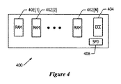
図4は例示的なDIMM(デュアルインラインメモリモジュール)400を示している。理解されるであろうように、メモリアレイ206は、幾つかの、典型的には8つのDIMMから構成されてよく、ここで各DIMM400は、DDR(ダブルデータレート)メモリチップ等の多重ランダムアクセスメモリ(RAM)集積回路又はチップ402[1:N]を含む。また、DIMM400はECC(誤り訂正符号)回路404を有していてよい。ECC回路404は、メモリ誤りを発見して且つ訂正することを可能にする誤り訂正符号を記憶する。更に、DIMM400はSPD(シリアルプレゼンスディテクト)回路406を有していてよい。SPD回路406は、DIMM400の動作範囲を指定するリードオンリ情報及びデータシートにおいて見出されるであろう他の同様の情報を含む。例えばSPD回路406は、DIMM400のメモリ記憶容量、最小サイクル時間等の動作パラメータ、CAS待ち時間、等を識別する。
FIG. 4 shows an exemplary DIMM (Dual Inline Memory Module) 400. As will be appreciated, the
システム初期化に際しては、各メモリモジュール206は初期化され且つ試験される必要がある。このことは、メモリモジュールのデータ投入状況(population)を検証することと、メモリの適切な動作(スタックビット無し)を検証することと、メモリを既知の値に初期化し又はクリーニングすることと、を含んでいてよい。各メモリモジュールは、任意のメモリ誤りを訂正するためにECCを周期的に利用することに基づいて洗われ(scrubbed)得る。
Upon system initialization, each
図5は本発明の選択された実施形態に従う最適化されたメモリ初期化及び試験シーケンス500のフロー図を示している。シーケンスは、ステップ502で、各処理ノードが他の処理ノード及びメモリと通信することができるようにシステムリンクを初期化することによって開始する。このことは、典型的には、ブートストラッププロセッサ上で動作しているBIOSによって行われる。代替的には、ハードワイヤードのシステム(hard wired system)においては、処理ノードは、システム電源投入に際して互いに及びメモリと通信するように自動的に構成されてよい。
FIG. 5 shows a flow diagram of an optimized memory initialization and
ステップ504では、ブートストラッププロセッサ(BSP)として指定された処理ノードは、メモリ初期化及び/又は試験プロセスが、メモリ初期化及び/又は試験タスクを複数のサブタスクに分割し、次いで各タスクを実行処理ノードに割り当てると共に分散させることよって開始するようにさせる。例えばBSPは、割り当てられたサブタスクと共に開始メッセージを各処理ノードへ送ることができる。追加的に又は代替的に、割り当てられたサブタスクがBSPによって送り届けられ得るように又は割り当てられたサブタスクが単一若しくは複数の実行処理ノードによってレトリーブされ(retrieved)得るように、メモリ初期化及び試験プロセスが開始すべきであることを示すビットが各処理ノード内に書き込まれてよい。代替的には、任意のプロセッサ上でのコード実行が1つ以上のレジスタに書き込む場合等に、指令された割り込みがプロセスを開始させることができる。書き込まれた値は、割り当てられたサブタスクに対して1つ以上のプロセッサが特定のアクションをとるようにそれらに指令することができる。例えば書き込まれた値は、指令された割り込みの目標を識別するノード識別子と、どこでコード実行を開始するのかを直接的に又は間接的に指定することを介して実行するための一連の命令及びサブタスクを示すベクターと、を含むことができる。必要であれば、目標とされているプロセッサがベクターにより指定される割り当てられたサブタスクの実行を開始することを促す開始メッセージを、目標とされているプロセッサにハードウエアメカニズムが送り届けることができる。
In
ステップ506では、各処理ノード202は、その割り当てられたメモリ初期化及び試験サブタスクを行い、それらは関連するメモリ206に対応していてもしていなくてもよい。図2に示される例示的な実装においては、コンピューティングシステム200は、4つのコア、1つの制御コア202[0]、及び3つのスレーブコア202[1:3]を含む。メモリ初期化/試験タスクは、制御コア202[0]によって複数のサブタスク(例えばサブタスク1、サブタスク2、サブタスク3等)に分割される。制御コア202[0]は、サブタスク1を第1のスレーブコア202[1]へ送り、サブタスク2を第2のスレーブコア202[2]へ送り、そしてサブタスク3を第3のスレーブコア202[3]へ送る。ステップ506では、各スレーブコア202[1:3]はそのサブタスクを受け取り、そして実行のためにそれをスケジューリングする。また、制御コア202[0]は、異なるサブタスクの実行を継続してよく、あるいはスレーブコア上での実行が完了するのを待ってよく又はそれ自身の別個のサブタスクを実行してよい。各スレーブコア202[1:3]は、それがタスクを処理する資源を有しているタイミングでサブタスクを実行し、その結果、実行の時間は他のスレーブコアと重なるかもしれないし重ならないかもしれない。結果として、割り当てられたメモリ初期化/試験サブタスクは、スレーブコアの資源の能力に応じて、コア202によってシリアルに又は並列に実行されることが可能である。サブタスク実行は、処理ノードによって又は各処理ノードのノースブリッジ内の回路によって行われ得る。
In
理解されるであろうように、制御コア及びスレーブコアは、独立した複数のプラットフォームシステム上にあってよい。そのような実装においては、制御コアは、各参加しているプラットフォームシステム上の1つ以上のコアが、その割り当てられている単一又は複数のサブタスクを各々処理し得るように、サブタスクを当該システムへ送る。このシナリオにおいては、実行はシリアルに又は並列になされてよい。メモリ初期化タスク実行の分散させられた性質の結果として、実行が並列に又はシリアルになされるという事実は、タスクの完了とは関係がない。タスクが並列に実行される場合、タスクはより速く完了するであろうが、データを転送する待ち時間は、制御コアでのシリアル化を結果としてもたらす可能性がある。 As will be appreciated, the control core and slave core may be on independent platform systems. In such an implementation, the control core assigns subtasks to the system so that one or more cores on each participating platform system can each process its assigned single or multiple subtasks. Send to. In this scenario, execution may be done serially or in parallel. The fact that execution is done in parallel or serial as a result of the distributed nature of memory initialization task execution has nothing to do with task completion. If the tasks are executed in parallel, the tasks will complete faster, but the latency to transfer data may result in serialization at the control core.
ステップ508では、各処理ノードは状況をBPSに報告する。状況報告することは、例えば、メモリ初期化及び試験の間に連続的であってよく、あるいは周期的であってよく、あるいはメモリ初期化及び試験が完了したときであってよい。また、状況報告は種々の方法で報告され得る。例えば、ブートストラッププロセッサは、各処理ノードへ周期的にクエリーを送り、割り当てられたサブタスクが実行され終わったかどうかを問い合わせることができる。代替的には、各処理ノードは、その状況をブートストラッププロセッサに示すメッセージを送ることができる。別の代替案としては、各処理ノードは、ローカルレジスタに又はブートストラッププロセッサのローカルメモリに書き込んで状況を報告することもできる。
In
全ての処理ノードがそれらの割り当てられたメモリ初期化/試験を完了した後に、ステップ510では、ブートストラッププロセッサがシステムブートを継続し、そして他の処理ノードは停止する。メモリ初期化/試験タスクが実行されるべきである場合(決定512が肯定)には、処理はステップ504で再び始まる。そうでない場合には、処理はステップ514で終了する。
After all processing nodes have completed their assigned memory initialization / test, at
メモリ初期化/試験サブタスクを異なる処理ノードに割り当てることによって、システムブートは極めて速く完了することができる。幾つかのサブタスクは先行するサブタスクの完了に依存し、また他のタスクは先行するサブタスクが完了するのを待たずにシーケンスからは自由に完了され得るのではあるけれど、タスクの依存性の有無を問わずにサブタスクを分割し、割り当て、そして分散させることによって、全体的な性能及び起動時間を改善することができる。このことは、サブタスクの幾つかは、タスクが実行順序になる前にそれらが現れ且つそれらの前に依存性のある実行を有していないことを待つ必要性なしに第1の処理ノードによって実行されるという理由で「システムブート(system boot)」又は「システムをブートすること(booting the system)」の時間が低減されるという事実に由来している。言うまでもなく、各サブタスクに対する個々の依存性を考慮に入れることによってブートストラッププロセッサがメモリ初期化/試験タスクをサブタスクに分割すれば、メモリ初期化は更に改善され得る。例えば、1つ以上の指定された処理ノードが他のサブタスクの結果に依存するサブタスクを割り当てられてよい一方で、1つ以上の他の指定された処理ノードは、先行する単一又は複数のサブタスクが完了するのを待たずにシーケンスからは自由に完了され得るサブタスクを割り当てられてよい。 By assigning memory initialization / test subtasks to different processing nodes, the system boot can be completed very quickly. Some subtasks depend on the completion of the preceding subtask, and other tasks can be completed freely from the sequence without waiting for the preceding subtask to complete, but whether there is a task dependency or not. By dividing, assigning, and distributing the subtasks regardless, overall performance and start-up time can be improved. This means that some of the subtasks are executed by the first processing node without having to wait for them to appear before they are in execution order and have no dependent execution before them Because of the fact that the time of "system boot" or "booting the system" is reduced. Needless to say, memory initialization can be further improved if the bootstrap processor splits the memory initialization / test task into subtasks by taking into account individual dependencies for each subtask. For example, one or more designated processing nodes may be assigned subtasks that depend on the results of other subtasks, while one or more other designated processing nodes may be preceded by a single or multiple subtasks Subtasks can be assigned that can be completed freely from the sequence without waiting for them to complete.
ここに説明されるように、分散させられたメモリ初期化ルーチンは、分散及び別個のノードによる実行のためにメモリタスクを分割することによって多重プロセッサシステム内の多重ノード間で分散させられるメモリを構成し、初期化し、そして試験することが可能なBIOSコードと共に実装されてよく、結果として改良された実行時間をもたらすことができる。例えば、1つのコアはSMバス(SMBus)(低速バス)からSPDを読み出すタスクを課せられ得る一方で、別のコアはSPD依存でない複雑な初期化タスクを実行することができる。開示される分散型処理手法はまた、特定のBIOSアルゴリズムの精度を改善することができる。例えば、より速い実行のためにBIOSが最適化されるようにアルゴリズムをトレーニングすることが開発されてきており、それにより遅延設定の最適配置を決定するために用いられ得るデータアイが生成される。しかし、生成されるデータアイは、トレーニングアルゴリズムを実行するコアにより処理され得るデータの量によって制限される。ここに開示される分散型処理アプローチは、主コアを用いてデータを集めそして情報を処理しまた結果を主コアに戻すシステム内の他のコアへの分散のために当該データを分割することによって精度を改善するために用いられ得る。開示される分割及び分散型スキームはまた結果として、割り当てられたサブタスクが順序を問わず実行される場合に、より速いブート時間をもたらす。更に別の可能な利益は、ブートストラッププロセッサにBIOS初期化タスクの全てを行わせることに代えて、サブタスクが各コアに分散させられるようにすることによって、処理コアがBIOS初期化の間に効率的に使用され得ることである。 As described herein, a distributed memory initialization routine configures memory that is distributed among multiple nodes in a multiprocessor system by dividing memory tasks for distribution and execution by separate nodes. Can be implemented with BIOS code that can be initialized, tested, and tested, resulting in improved execution time. For example, one core may be tasked with reading the SPD from the SM bus (SMBus) (slow speed bus) while another core may perform complex initialization tasks that are not SPD dependent. The disclosed distributed processing approach can also improve the accuracy of certain BIOS algorithms. For example, it has been developed to train algorithms so that the BIOS is optimized for faster execution, thereby generating data eyes that can be used to determine the optimal placement of delay settings. However, the data eye generated is limited by the amount of data that can be processed by the core executing the training algorithm. The distributed processing approach disclosed here collects data using the main core and processes the information and splits the data for distribution to other cores in the system that returns the results to the main core. Can be used to improve accuracy. The disclosed split and distributed scheme also results in faster boot times when assigned subtasks are executed in any order. Yet another possible benefit is that instead of having the bootstrap processor do all of the BIOS initialization tasks, the processing cores are more efficient during BIOS initialization by allowing subtasks to be distributed across each core. It can be used in the future.
更なる例、及びメモリ初期化タスクがどのようにして分割されそして複数の処理ノードにわたって分散させられ得るのかの説明を提供するために、以下のメモリ初期化ルーチン又はアルゴリズムが次に説明され、ここでサブタスクstの総数はシステム内のコアの総数以下である。 In order to provide further examples and explanations of how the memory initialization task can be split and distributed across multiple processing nodes, the following memory initialization routine or algorithm is described next, where The total number of subtasks st is less than or equal to the total number of cores in the system.
T= {st[1]+st[2]+st[3]+…st[X]}、ここでstはメモリ初期化サブタスクである; T = {st [1] + st [2] + st [3] +... St [X]}, where st is a memory initialization subtask;
C0= 「st」を結合して「T」を生成することに関与する主初期化コア; C0 = the main initialization core involved in combining “st” to produce “T”;
c[n]= サブタスクコア、但しn={1,…,N}; c [n] = subtask core, where n = {1,..., N};
N= N≧Xとなるコアの最大数; The maximum number of cores where N = N ≧ X;
X= 任意のTに対するサブタスクの最大数; X = the maximum number of subtasks for any T;
n− 現在のコア数; n-current number of cores;
x− 現在のサブタスク数; x-current number of subtasks;
ステップ1− サブタスクをコアに分散させる; Step 1-Distribute subtasks to the core;
ステップ2− c[n]に対して; Step 2- for c [n];
ステップ3− st[x]に対して;
ステップ4− c0からc[n]までst[x]初期化情報及びコードを送る; Step 4- Send st [x] initialization information and code from c0 to c [n];
ステップ5− c[n]はs[x]の実行を開始; Step 5- c [n] starts execution of s [x];
ステップ6− c0はc[n]からst[x]結果を受け取り実行を開始; Step 6-c0 receives the st [x] result from c [n] and starts execution;
ステップ7− c0はn及びxをインクリメント; Step 7-c0 increments n and x;
ステップ8− c0は全てのXに対してステップ2〜7を繰り返す; Step 8-c0 repeats steps 2-7 for all Xs;
ステップ9− n=Nの場合にステップ10へ移動; Step 9—Go to Step 10 if n = N;
ステップ10− c0は分散させられたサブタスクデータを収集; Step 10-c0 collects distributed subtask data;
ステップ11− c[n]に対して; Step 11—For c [n];
ステップ12− c0はc[n]からst[x]データを要求; Step 12-c0 requests st [x] data from c [n];
ステップ13− c[n]は実行を完了して結果をc0へ送る; Step 13-c [n] completes execution and sends the result to c0;
ステップ14− c0はn及びxをインクリメント; Step 14-c0 increments n and x;
ステップ15− c0は全てのn=Nになるまで全てのXに対してステップ11〜14を繰り返す; Step 15-c0 repeats Steps 11-14 for all X until all n = N;
ステップ16− c0は全てのst[1−X]からのデータを再結合することによってTを生成; Step 16-c0 generates T by recombining data from all st [1-X];
ステップ17− 全てのステップが次のタスクのために繰り返される。 Step 17-All steps are repeated for the next task.
理解されるであろうように、前述のルーチンは、疑似コード形態で表現され得るし且つ/又は特定の命令セットアーキテクチャのためのそれらが使用している対応するアセンブリ言語若しくは高レベル言語コードへとトランスレートされ得る。また、ここに説明される動作は、コンピュータシステムユーザによって直接エントリされたコマンド及び/又はソフトウエアモジュールによって実行されるステップを含み得る。ここに参照される任意のステップの機能性は、モジュール又はモジュールの一部の機能性に対応していてよい。ソフトウエアモジュールに加えて、上述のフロー又はフローの一部は、アプリケーション命令として実装され得る。ここに参照される動作は、モジュール又はモジュールの一部(例えばソフトウエア、ファームウエア、又はハードウエアのモジュール)であってよい。例えば、ここで論じられるソフトウエアモジュールは、スクリプト、バッチ若しくは他の実行可能なファイル又はそのようなファイルの組み合わせ及び/若しくは一部を含んでいてよい。ソフトウエアモジュールは、コンピュータ可読媒体上でエンコードされるコンピュータプログラム又はそのサブルーチンを含んでいてよい。 As will be appreciated, the aforementioned routines can be expressed in pseudocode form and / or into corresponding assembly language or high-level language code that they are using for a particular instruction set architecture. Can be translated. Also, the operations described herein may include steps performed by commands and / or software modules entered directly by a computer system user. The functionality of any step referenced herein may correspond to the functionality of a module or part of a module. In addition to software modules, the above-described flows or portions of flows may be implemented as application instructions. The operations referred to herein may be modules or parts of modules (eg, software, firmware, or hardware modules). For example, the software modules discussed herein may include scripts, batches or other executable files or combinations and / or portions of such files. The software module may include a computer program encoded on a computer readable medium or a subroutine thereof.
加えて、当業者であれば、モジュール間の境界は単に例示的なものであり、また代替的な実施形態はモジュールを合併し又はその代わりにモジュールの機能性の分解を課する場合があることを理解するはずである。例えば、ここで論じられるモジュールは、多重コンピュータ処理として実行されるべきサブモジュールへと分解されてよい。また、代替的な実施形態は特定のモジュール又はサブモジュールの多重インスタンスを結合してよい。更に、当業者であれば、例示的な実施形態において説明される動作は例示のみを目的としていることを認識するはずである。本発明に従う追加的な動作においては、動作は結合されてよく、あるいは動作の機能性は分散させられてよい。従って、ここに説明されるフロー、その動作、及びそのためのモジュールは、フローの動作を実行するように構成されるコンピュータシステム上で実行されてよく且つ/又はコンピュータ可読媒体から実行されてよい。フローは、フローを実行するコンピュータシステムを構成するための機械可読媒体及び/又はコンピュータ可読媒体において具現化されてよい。従って、ソフトウエアモジュールは、コンピュータシステムメモリ内に記憶され且つ/又はコンピュータシステムメモリへ伝送されて、モジュールの機能を行うためのコンピュータシステムを構成してよい。 In addition, those skilled in the art will recognize that the boundaries between modules are merely exemplary, and that alternative embodiments may merge modules or instead impose a breakdown of module functionality. Should understand. For example, the modules discussed herein may be broken down into submodules that are to be executed as multi-computer processing. Alternate embodiments may also combine multiple instances of a particular module or submodule. Further, those skilled in the art will recognize that the operations described in the exemplary embodiments are for illustrative purposes only. In additional operations according to the present invention, the operations may be combined or the functionality of the operations may be distributed. Accordingly, the flows described herein, operations thereof, and modules therefor may be executed on a computer system configured to perform the operations of the flows and / or executed from a computer-readable medium. The flow may be embodied in a machine readable medium and / or a computer readable medium for configuring a computer system that executes the flow. Accordingly, software modules may be stored in and / or transmitted to computer system memory to constitute a computer system for performing the functions of the module.
上に開示される特定の実施形態は例示のみを目的としており、また本発明は異なる方法であるがここでの教示の利益を有する当業者に明らかな均等な方法において修正されそして実施され得るので、上に開示される特定の実施形態は本発明を限定するものとして解釈されるべきではない。従って、前述の説明は、記載されている特定の形態に本発明を限定することを意図するものではないが、一方で、本発明の精神及び範囲の最も広い形態から逸脱することなしに当業者が種々の変更、置換及び代替をなし得ると当業者が理解するはずであるように添付の特許請求の範囲によって定義される本発明の精神及び範囲内に含まれるであろう代替、修正、及び均等なものに及ぶことが意図されている。 The specific embodiments disclosed above are for illustrative purposes only, and the present invention may be modified and implemented in an equivalent manner apparent to those skilled in the art that are different ways but have the benefit of the teachings herein. The specific embodiments disclosed above should not be construed as limiting the invention. Accordingly, the foregoing description is not intended to limit the invention to the particular form described, but may be made by those skilled in the art without departing from the broadest form of the spirit and scope of the invention. As will be appreciated by those skilled in the art that various changes, substitutions, and alternatives may be made, alternatives, modifications, and within the spirit and scope of the invention as defined by the appended claims It is intended to cover the equivalent.
Claims (17)
制御処理ノードでメモリ初期化タスクを複数のメモリ初期化サブタスクに分割することと、
対応する処理ノードを各メモリ初期化サブタスクが有するように、前記複数のメモリ初期化サブタスクを前記複数の処理ノードの間で分散させることと、
前記対応する処理ノードで各メモリ初期化サブタスクを実行してサブタスク結果を生成することと、
前記複数の処理ノードからのサブタスク結果を前記制御処理ノードで結合することと、を備え、
前記複数のメモリ初期化サブタスクは、前記複数の処理ノードで並列に又はシーケンスに実行され得るものであって、
前記分散させることは、
シリアルプレゼンスディテクト(SPD)値をデュアルインラインメモリモジュールから読み出すメモリ初期化サブタスクを、前記複数の処理ノードの1つに割り当てることと、
前記SPD値に依存しないメモリ初期化サブタスクを、前記複数の処理ノードの他の1つに割り当てることとを含む、
方法。 A method of causing a plurality of processing nodes to perform a boot processing task including a memory initialization task,
Dividing the memory initialization task into multiple memory initialization subtasks at the control processing node;
Distributing the plurality of memory initialization subtasks among the plurality of processing nodes such that each memory initialization subtask has a corresponding processing node;
Executing each memory initialization subtask on the corresponding processing node to generate a subtask result;
Combining subtask results from the plurality of processing nodes at the control processing node,
The plurality of memory initialization subtasks may be executed in parallel or in sequence on the plurality of processing nodes,
The dispersing is
Assigning a memory initialization subtask for reading a serial presence detect (SPD) value from a dual in-line memory module to one of the plurality of processing nodes;
Assigning a memory initialization subtask independent of the SPD value to another one of the plurality of processing nodes;
Method.
複数の処理ノードとを含むコンピュータシステムであって、
前記複数の処理ノードの各々は、
プロセッサコアと、前記複数の処理ノードの他の少なくとも1つに接続するための通信インタフェースと、前記システムメモリへの及び前記システムメモリからのデータフローを管理するためのメモリ制御器とを含み、
前記複数の処理ノードは、
マスター処理ノードと、複数の実行処理ノードとを含み、
前記マスター処理ノードは、
メモリ初期化タスクを複数のメモリ初期化サブタスクに分割することと、割り当てられたメモリ初期化サブタスクの各々が対応する実行処理ノードを有するように、前記複数のメモリ初期化サブタスクを前記複数の実行処理ノードに割り当てることとによって、前記メモリ初期化タスクを前記システムメモリに対して実行するように構成されており、
前記複数のメモリ初期化サブタスクは、
前記複数の実行処理ノードの1つに割り当てられたメモリ初期化サブタスクが、前記複数の実行処理ノードの他の1つに割り当てられた他のメモリ初期化サブタスクに依存することなく順序を問わずに実行可能となるように、前記複数の実行処理ノードで並列に又はシーケンスに実行され得るものであり、
前記割り当てることは、
シリアルプレゼンスディテクト(SPD)値を前記システムメモリのデュアルインラインメモリモジュールから読み出すメモリ初期化サブタスクを、前記複数の処理ノードの1つに割り当てることと、
前記SPD値に依存しないメモリ初期化サブタスクを、前記複数の処理ノードの他の1つに割り当てることとを含む、
コンピュータシステム。 System memory,
A computer system including a plurality of processing nodes,
Each of the plurality of processing nodes is
A processor core; a communication interface for connecting to at least one other of the plurality of processing nodes; and a memory controller for managing data flow to and from the system memory;
The plurality of processing nodes are:
Including a master processing node and a plurality of execution processing nodes;
The master processing node is
Dividing the memory initialization task into a plurality of memory initialization subtasks, and assigning the plurality of memory initialization subtasks to the plurality of execution processes so that each assigned memory initialization subtask has a corresponding execution processing node. by and assigning the node, is configured to run against the system memory the memory initialization tasks,
The plurality of memory initialization subtasks include:
The memory initialization subtask assigned to one of the plurality of execution processing nodes does not depend on other memory initialization subtasks assigned to the other one of the plurality of execution processing nodes regardless of the order. Can be executed in parallel or in sequence on the plurality of execution processing nodes so as to be executable,
The assigning is
Assigning a memory initialization subtask for reading a serial presence detect (SPD) value from a dual in-line memory module of the system memory to one of the plurality of processing nodes;
Assigning a memory initialization subtask independent of the SPD value to another one of the plurality of processing nodes;
Computer system.
複数の処理ノードとを含むコンピュータシステムであって、
前記複数の処理ノードの各々は、
プロセッサコアと、前記メモリアレイと通信するためのメモリ制御器と、前記複数の処理ノードの他の少なくとも1つに接続するための通信インタフェースとを含み、
前記複数の処理ノードのうち第1の処理ノードは、
メモリ初期化タスクを複数のサブタスクに分割し、前記複数のサブタスクを前記複数の処理ノードのうち他の処理ノードに割り当て、
前記複数の処理ノードの各々は、
割り当てられたサブタスクを実行しながら前記メモリアレイの任意の部分にアクセスするとともに、サブタスク実行結果を前記複数の処理ノードのうち前記第1の処理ノードに戻すことができ、これにより、前記複数の処理ノードが前記メモリアレイのメモリ初期化を実行することを可能にし、
前記複数のサブタスクを前記複数の処理ノードのうち他の処理ノードに割り当てることは、
シリアルプレゼンスディテクト(SPD)値をデュアルインラインメモリモジュールから読み出すメモリ初期化サブタスクを、前記複数の処理ノードの1つに割り当てることと、
前記SPD値に依存しないメモリ初期化サブタスクを、前記複数の処理ノードの他の1つに割り当てることとを含む、
コンピュータシステム。 A memory array;
A computer system including a plurality of processing nodes,
Each of the plurality of processing nodes is
A processor core, a memory controller for communicating with the memory array, and a communication interface for connecting to at least one other of the plurality of processing nodes;
A first processing node of the plurality of processing nodes is
Dividing the memory initialization task into a plurality of subtasks, assigning the plurality of subtasks to other processing nodes of the plurality of processing nodes;
Each of the plurality of processing nodes is
While executing an assigned subtask, any part of the memory array can be accessed, and a subtask execution result can be returned to the first processing node among the plurality of processing nodes. Allowing the node to perform memory initialization of the memory array;
Assigning the plurality of subtasks to another processing node of the plurality of processing nodes,
Assigning a memory initialization subtask for reading a serial presence detect (SPD) value from a dual in-line memory module to one of the plurality of processing nodes;
Assigning a memory initialization subtask independent of the SPD value to another one of the plurality of processing nodes;
Computer system.
Applications Claiming Priority (3)
| Application Number | Priority Date | Filing Date | Title |
|---|---|---|---|
| US12/624,626 US8307198B2 (en) | 2009-11-24 | 2009-11-24 | Distributed multi-core memory initialization |
| US12/624,626 | 2009-11-24 | ||
| PCT/US2010/057561 WO2011066202A1 (en) | 2009-11-24 | 2010-11-22 | Distributed multi-core memory initialization |
Publications (3)
| Publication Number | Publication Date |
|---|---|
| JP2013512509A JP2013512509A (en) | 2013-04-11 |
| JP2013512509A5 JP2013512509A5 (en) | 2014-01-16 |
| JP5646644B2 true JP5646644B2 (en) | 2014-12-24 |
Family
ID=43501297
Family Applications (1)
| Application Number | Title | Priority Date | Filing Date |
|---|---|---|---|
| JP2012541131A Active JP5646644B2 (en) | 2009-11-24 | 2010-11-22 | Distributed multi-core memory initialization |
Country Status (6)
| Country | Link |
|---|---|
| US (2) | US8307198B2 (en) |
| EP (1) | EP2504761A1 (en) |
| JP (1) | JP5646644B2 (en) |
| KR (1) | KR101623892B1 (en) |
| CN (1) | CN102648453B (en) |
| WO (1) | WO2011066202A1 (en) |
Families Citing this family (49)
| Publication number | Priority date | Publication date | Assignee | Title |
|---|---|---|---|---|
| CN101872308A (en) * | 2009-04-25 | 2010-10-27 | 鸿富锦精密工业(深圳)有限公司 | Memory bar control system and control method thereof |
| WO2012001777A1 (en) * | 2010-06-29 | 2012-01-05 | 富士通株式会社 | Multi-core processor system, communication control method, and communication control program |
| US9936209B2 (en) * | 2011-08-11 | 2018-04-03 | The Quantum Group, Inc. | System and method for slice processing computer-related tasks |
| US8954639B2 (en) * | 2011-09-06 | 2015-02-10 | International Business Machines Corporation | Integrated link calibration and multi-processor topology discovery |
| US20130081050A1 (en) * | 2011-09-23 | 2013-03-28 | Elwha LLC, a limited liability company of the State of Delaware | Acquiring and transmitting tasks and subtasks to interface devices |
| US9269063B2 (en) | 2011-09-23 | 2016-02-23 | Elwha Llc | Acquiring and transmitting event related tasks and subtasks to interface devices |
| US20130081049A1 (en) * | 2011-09-23 | 2013-03-28 | Elwha LLC, a limited liability company of the State of Delaware | Acquiring and transmitting tasks and subtasks to interface devices |
| US9336130B2 (en) * | 2011-11-30 | 2016-05-10 | Sandisk Technologies Inc. | Methods, systems, and computer readable media for providing basic input/output system (BIOS) data and non-BIOS data on the same non-volatile memory |
| WO2013101093A1 (en) * | 2011-12-29 | 2013-07-04 | Intel Corporation | Initialization of multi-core processing system |
| WO2013142861A1 (en) | 2012-03-23 | 2013-09-26 | Polycore Software, Inc. | Apparatus and method for providing a multicore programming platform |
| CN102779075B (en) * | 2012-06-28 | 2014-12-24 | 华为技术有限公司 | Method, device and system for scheduling in multiprocessor nuclear system |
| KR20140036731A (en) * | 2012-09-18 | 2014-03-26 | 한국전자통신연구원 | Development method and system of application program |
| FR2996020A1 (en) * | 2012-09-27 | 2014-03-28 | Thales Sa | Digital processing device for use in radar system, has allowance unit arranged to allow next task or sub-task to be carried out with slave cores determined according to indicators of state of register of slave cores |
| CN102999385B (en) * | 2012-11-06 | 2016-05-25 | 国网山东省电力公司枣庄供电公司 | Multiprocessor cooperative processing method in computing equipment |
| CN103870334B (en) * | 2012-12-18 | 2017-05-31 | 中国移动通信集团公司 | A kind of method for allocating tasks and device of extensive vulnerability scanning |
| KR102183274B1 (en) * | 2013-01-16 | 2020-11-26 | 에스케이플래닛 주식회사 | System and method for distributed processing, and apparatus applied to the same |
| KR101766695B1 (en) * | 2013-03-15 | 2017-08-09 | 후아웨이 테크놀러지 컴퍼니 리미티드 | Booting method for computer system with multiple central processing units |
| JP5942904B2 (en) * | 2013-03-19 | 2016-06-29 | 株式会社デンソー | Processing equipment |
| EP2981885A4 (en) * | 2013-04-03 | 2016-11-02 | Hewlett Packard Development Co | Modifying a flow of operations to be executed in a plurality of execution environments |
| WO2014209406A1 (en) * | 2013-06-29 | 2014-12-31 | Intel Corporation | On-chip mesh interconnect |
| US10229043B2 (en) * | 2013-07-23 | 2019-03-12 | Intel Business Machines Corporation | Requesting memory spaces and resources using a memory controller |
| US9792112B2 (en) | 2013-08-28 | 2017-10-17 | Via Technologies, Inc. | Propagation of microcode patches to multiple cores in multicore microprocessor |
| US9471133B2 (en) | 2013-08-28 | 2016-10-18 | Via Technologies, Inc. | Service processor patch mechanism |
| US9465432B2 (en) | 2013-08-28 | 2016-10-11 | Via Technologies, Inc. | Multi-core synchronization mechanism |
| CN105580001A (en) * | 2013-09-27 | 2016-05-11 | 慧与发展有限责任合伙企业 | Processing a hybrid flow associated with a service class |
| US9658858B2 (en) | 2013-10-16 | 2017-05-23 | Xilinx, Inc. | Multi-threaded low-level startup for system boot efficiency |
| JP6206097B2 (en) | 2013-11-01 | 2017-10-04 | 富士通株式会社 | Information processing apparatus, activation method, and activation program |
| US9239711B1 (en) * | 2013-12-31 | 2016-01-19 | Google Inc. | Run benchmark or analysis tools against massive repository of archived webpages on machines in the cloud for continuous builds or AD-HOC requests |
| US10108253B2 (en) | 2014-01-30 | 2018-10-23 | Hewlett Packard Enterprise Development Lp | Multiple compute nodes |
| CN104520811B (en) * | 2014-05-09 | 2017-07-28 | 华为技术有限公司 | The system and method for the startup time of computer of the optimization with multiple central processing units |
| WO2015169068A1 (en) * | 2014-05-09 | 2015-11-12 | Huawei Technologies Co., Ltd. | System and method thereof to optimize boot time of computers having multiple cpus |
| CN105100179B (en) * | 2014-05-23 | 2018-10-19 | 杭州华为数字技术有限公司 | Server cluster system |
| US9710381B2 (en) | 2014-06-18 | 2017-07-18 | International Business Machines Corporation | Method and apparatus for cache memory data processing |
| CN104298576B (en) * | 2014-09-25 | 2018-09-04 | 小米科技有限责任公司 | terminal test method and device |
| CN105528199B (en) * | 2014-09-30 | 2019-04-19 | 华为技术有限公司 | A kind of processing method and processing device of node |
| WO2016068903A1 (en) | 2014-10-29 | 2016-05-06 | Hewlett Packard Enterprise Development Lp | Trans-fabric instruction set for a communication fabric |
| US20160164696A1 (en) * | 2014-12-08 | 2016-06-09 | Ebay Inc. | Modular internet of things |
| US10248487B1 (en) * | 2015-01-27 | 2019-04-02 | Violin Systems Llc | Error recovery for multi-stage simultaneously running tasks |
| US10528443B2 (en) | 2015-01-30 | 2020-01-07 | Samsung Electronics Co., Ltd. | Validation of multiprocessor hardware component |
| US10193826B2 (en) | 2015-07-15 | 2019-01-29 | Intel Corporation | Shared mesh |
| TWI554945B (en) * | 2015-08-31 | 2016-10-21 | 晨星半導體股份有限公司 | Routine task allocating method and multicore computer using the same |
| CN106708727B (en) * | 2016-08-03 | 2020-04-28 | 腾讯科技(深圳)有限公司 | Distributed virus characteristic sample verification method and system |
| US11074085B2 (en) * | 2017-09-26 | 2021-07-27 | Intel Corporation | Methods and apparatus for boot time reduction in a processor and programmable logic device environment |
| CN111133414A (en) | 2017-12-25 | 2020-05-08 | 英特尔公司 | Multithreading parallel computing platform before memory initialization |
| US11042644B2 (en) * | 2018-02-01 | 2021-06-22 | Quixant Plc | Method and system for security verification in a booting process with a multi-core processor |
| CN109448777A (en) * | 2018-11-12 | 2019-03-08 | 郑州云海信息技术有限公司 | A kind of test method and device of NVME solid state hard disk |
| CN109581925A (en) * | 2018-12-05 | 2019-04-05 | 北京和利时系统工程有限公司 | A kind of task processing method and device, computer readable storage medium |
| US20200341776A1 (en) * | 2020-07-07 | 2020-10-29 | Krishnaprasad H | Apparatus for initializing memory using a hardware engine for minimizing boot time |
| JP7460743B1 (en) | 2022-12-27 | 2024-04-02 | Necプラットフォームズ株式会社 | MEMORY CONTROLLER AND MEMORY CONTROLLER CONTROL METHOD |
Family Cites Families (20)
| Publication number | Priority date | Publication date | Assignee | Title |
|---|---|---|---|---|
| EP0817998A4 (en) * | 1995-03-31 | 1998-09-23 | Intel Corp | Memory testing in a multiple processor computer system |
| US5768585A (en) * | 1995-11-21 | 1998-06-16 | Intel Corporation | System and method for synchronizing multiple processors during power-on self testing |
| US6158000A (en) * | 1998-09-18 | 2000-12-05 | Compaq Computer Corporation | Shared memory initialization method for system having multiple processor capability |
| US6336185B1 (en) * | 1998-09-24 | 2002-01-01 | Phoenix Technologies Ltd. | Use of other processors during BIOS boot sequence to minimize boot time |
| US6766474B2 (en) * | 2000-12-21 | 2004-07-20 | Intel Corporation | Multi-staged bios-based memory testing |
| JP3773195B2 (en) * | 2002-10-25 | 2006-05-10 | インターナショナル・ビジネス・マシーンズ・コーポレーション | Memory module, information processing apparatus, initial setting method for memory module, and program |
| US7065688B1 (en) * | 2003-02-19 | 2006-06-20 | Advanced Micro Devices, Inc. | Simultaneous multiprocessor memory testing and initialization |
| US7194660B2 (en) * | 2003-06-23 | 2007-03-20 | Newisys, Inc. | Multi-processing in a BIOS environment |
| US7539909B2 (en) * | 2003-09-30 | 2009-05-26 | Intel Corporation | Distributed memory initialization and test methods and apparatus |
| US7251744B1 (en) * | 2004-01-21 | 2007-07-31 | Advanced Micro Devices Inc. | Memory check architecture and method for a multiprocessor computer system |
| US7281127B2 (en) * | 2004-12-27 | 2007-10-09 | Intel Corporation | Concurrent processing of operations in a boot sequence to initialize a storage device including an operating system loader to load |
| JP4569368B2 (en) * | 2005-04-26 | 2010-10-27 | 日本電気株式会社 | Computer system, memory initialization method, and computer system program |
| WO2007025112A1 (en) * | 2005-08-23 | 2007-03-01 | Advanced Micro Devices, Inc. | Method for proactive synchronization within a computer system |
| US7526639B2 (en) * | 2006-02-13 | 2009-04-28 | International Business Machines Corporation | Method to enhance boot time using redundant service processors |
| US7779244B2 (en) * | 2006-12-28 | 2010-08-17 | Intel Corporation | Multi-socket boot |
| JP4234766B1 (en) * | 2007-10-31 | 2009-03-04 | 株式会社東芝 | Electronic device and control method thereof |
| CN101464813A (en) * | 2007-12-19 | 2009-06-24 | 国际商业机器公司 | Automatic workload distribution system and method for multi-core processor |
| JP5068188B2 (en) * | 2008-01-21 | 2012-11-07 | インターナショナル・ビジネス・マシーンズ・コーポレーション | Method, computer program, and system for performing memory tests |
| US20090193175A1 (en) * | 2008-01-28 | 2009-07-30 | Advanced Micro Devices, Inc. | Identification of an onboard memory buffer device from a system address |
| JP5217520B2 (en) * | 2008-03-06 | 2013-06-19 | 株式会社リコー | Electronics |
-
2009
- 2009-11-24 US US12/624,626 patent/US8307198B2/en active Active
-
2010
- 2010-11-22 CN CN201080055347.6A patent/CN102648453B/en active Active
- 2010-11-22 KR KR1020127014955A patent/KR101623892B1/en active IP Right Grant
- 2010-11-22 EP EP10782514A patent/EP2504761A1/en not_active Ceased
- 2010-11-22 JP JP2012541131A patent/JP5646644B2/en active Active
- 2010-11-22 WO PCT/US2010/057561 patent/WO2011066202A1/en active Application Filing
-
2012
- 2012-10-10 US US13/648,648 patent/US8566570B2/en active Active
Also Published As
| Publication number | Publication date |
|---|---|
| US20130042096A1 (en) | 2013-02-14 |
| KR20120112454A (en) | 2012-10-11 |
| WO2011066202A1 (en) | 2011-06-03 |
| JP2013512509A (en) | 2013-04-11 |
| US8566570B2 (en) | 2013-10-22 |
| KR101623892B1 (en) | 2016-05-24 |
| US20110126209A1 (en) | 2011-05-26 |
| US8307198B2 (en) | 2012-11-06 |
| CN102648453A (en) | 2012-08-22 |
| CN102648453B (en) | 2015-11-25 |
| EP2504761A1 (en) | 2012-10-03 |
Similar Documents
| Publication | Publication Date | Title |
|---|---|---|
| JP5646644B2 (en) | Distributed multi-core memory initialization | |
| US9921949B2 (en) | Software testing | |
| US7065688B1 (en) | Simultaneous multiprocessor memory testing and initialization | |
| JP2009151774A (en) | Method, device and system for autonomic workload distribution on multicore processor | |
| JP2013512509A5 (en) | ||
| JP2014225242A (en) | Method for booting heterogeneous system and presenting symmetric core view | |
| US11893379B2 (en) | Interface and warm reset path for memory device firmware upgrades | |
| EP4102359A1 (en) | Systems, apparatus and methods for rapid peripheral component interconnect express (pcie) system boot | |
| US20160048184A1 (en) | Sharing firmware among agents in a computing node | |
| Houdek et al. | Towards predictable execution model on ARM-based heterogeneous platforms | |
| US8626965B2 (en) | Using a DMA engine to automatically validate DMA data paths | |
| Cilku et al. | A TDMA-based arbitration scheme for mixed-criticality multicore platforms | |
| CN116881929A (en) | Safety protection method and device, electronic equipment and substrate controller chip | |
| Ding et al. | A unified opencl-flavor programming model with scalable hybrid hardware platform on fpgas | |
| US20130007768A1 (en) | Atomic operations on multi-socket platforms | |
| EP4064041A1 (en) | Platform hardening for bootloaders via reference firmware | |
| US20150042665A1 (en) | Gpgpu systems and services | |
| US8694975B2 (en) | Programming system in multi-core environment, and method and program of the same | |
| JP2017505031A (en) | Dynamic interconnect using partitioning and platform prototyping in emulation | |
| Cvek et al. | GNU/Linux and reconfigurable multiprocessor FPGA platform | |
| US7124311B2 (en) | Method for controlling processor in active/standby mode by third decoder based on instructions sent to a first decoder and the third decoder | |
| Dumitru et al. | USING CLOUDS FOR FPGA DEVELOPMENT-A COMMERCIAL PERSPECTIVE. | |
| US9336011B2 (en) | Server and booting method | |
| Viktorin et al. | Framework for fast prototyping of applications running on reconfigurable system on chip | |
| Misawa et al. | Dynamic Reconfiguration of Computer Platforms at the Hardware Device Level for High Performance Computing Infrastructure as a Service |
Legal Events
| Date | Code | Title | Description |
|---|---|---|---|
| A521 | Request for written amendment filed |
Free format text: JAPANESE INTERMEDIATE CODE: A523 Effective date: 20131122 |
|
| A621 | Written request for application examination |
Free format text: JAPANESE INTERMEDIATE CODE: A621 Effective date: 20131122 |
|
| A871 | Explanation of circumstances concerning accelerated examination |
Free format text: JAPANESE INTERMEDIATE CODE: A871 Effective date: 20131122 |
|
| A975 | Report on accelerated examination |
Free format text: JAPANESE INTERMEDIATE CODE: A971005 Effective date: 20131224 |
|
| A131 | Notification of reasons for refusal |
Free format text: JAPANESE INTERMEDIATE CODE: A131 Effective date: 20140108 |
|
| A601 | Written request for extension of time |
Free format text: JAPANESE INTERMEDIATE CODE: A601 Effective date: 20140403 |
|
| A602 | Written permission of extension of time |
Free format text: JAPANESE INTERMEDIATE CODE: A602 Effective date: 20140410 |
|
| A601 | Written request for extension of time |
Free format text: JAPANESE INTERMEDIATE CODE: A601 Effective date: 20140508 |
|
| A602 | Written permission of extension of time |
Free format text: JAPANESE INTERMEDIATE CODE: A602 Effective date: 20140515 |
|
| A521 | Request for written amendment filed |
Free format text: JAPANESE INTERMEDIATE CODE: A523 Effective date: 20140519 |
|
| A131 | Notification of reasons for refusal |
Free format text: JAPANESE INTERMEDIATE CODE: A131 Effective date: 20140611 |
|
| A521 | Request for written amendment filed |
Free format text: JAPANESE INTERMEDIATE CODE: A523 Effective date: 20140905 |
|
| TRDD | Decision of grant or rejection written | ||
| A01 | Written decision to grant a patent or to grant a registration (utility model) |
Free format text: JAPANESE INTERMEDIATE CODE: A01 Effective date: 20141007 |
|
| A61 | First payment of annual fees (during grant procedure) |
Free format text: JAPANESE INTERMEDIATE CODE: A61 Effective date: 20141105 |
|
| R150 | Certificate of patent or registration of utility model |
Ref document number: 5646644 Country of ref document: JP Free format text: JAPANESE INTERMEDIATE CODE: R150 |
|
| R250 | Receipt of annual fees |
Free format text: JAPANESE INTERMEDIATE CODE: R250 |
|
| R250 | Receipt of annual fees |
Free format text: JAPANESE INTERMEDIATE CODE: R250 |
|
| R250 | Receipt of annual fees |
Free format text: JAPANESE INTERMEDIATE CODE: R250 |
|
| R250 | Receipt of annual fees |
Free format text: JAPANESE INTERMEDIATE CODE: R250 |
|
| R250 | Receipt of annual fees |
Free format text: JAPANESE INTERMEDIATE CODE: R250 |
|
| R250 | Receipt of annual fees |
Free format text: JAPANESE INTERMEDIATE CODE: R250 |
|
| R250 | Receipt of annual fees |
Free format text: JAPANESE INTERMEDIATE CODE: R250 |