JP5609574B2 - Directional coupler - Google Patents
Directional coupler Download PDFInfo
- Publication number
- JP5609574B2 JP5609574B2 JP2010253884A JP2010253884A JP5609574B2 JP 5609574 B2 JP5609574 B2 JP 5609574B2 JP 2010253884 A JP2010253884 A JP 2010253884A JP 2010253884 A JP2010253884 A JP 2010253884A JP 5609574 B2 JP5609574 B2 JP 5609574B2
- Authority
- JP
- Japan
- Prior art keywords
- directional coupler
- main line
- capacitor
- line
- modification
- Prior art date
- Legal status (The legal status is an assumption and is not a legal conclusion. Google has not performed a legal analysis and makes no representation as to the accuracy of the status listed.)
- Active
Links
Images


Classifications
-
- H—ELECTRICITY
- H01—ELECTRIC ELEMENTS
- H01P—WAVEGUIDES; RESONATORS, LINES, OR OTHER DEVICES OF THE WAVEGUIDE TYPE
- H01P5/00—Coupling devices of the waveguide type
- H01P5/12—Coupling devices having more than two ports
- H01P5/16—Conjugate devices, i.e. devices having at least one port decoupled from one other port
- H01P5/18—Conjugate devices, i.e. devices having at least one port decoupled from one other port consisting of two coupled guides, e.g. directional couplers
- H01P5/184—Conjugate devices, i.e. devices having at least one port decoupled from one other port consisting of two coupled guides, e.g. directional couplers the guides being strip lines or microstrips
- H01P5/185—Edge coupled lines
-
- H—ELECTRICITY
- H01—ELECTRIC ELEMENTS
- H01P—WAVEGUIDES; RESONATORS, LINES, OR OTHER DEVICES OF THE WAVEGUIDE TYPE
- H01P5/00—Coupling devices of the waveguide type
- H01P5/12—Coupling devices having more than two ports
- H01P5/16—Conjugate devices, i.e. devices having at least one port decoupled from one other port
- H01P5/18—Conjugate devices, i.e. devices having at least one port decoupled from one other port consisting of two coupled guides, e.g. directional couplers
Description
本発明は、高周波信号を伝搬する主線路と、主線路に対して平行に配置され主線路に電磁気的に結合された副線路とを備える方向性結合器に関する。 The present invention relates to a directional coupler including a main line that propagates a high-frequency signal and a sub-line that is disposed in parallel to the main line and electromagnetically coupled to the main line.
方向性結合器は、高周波信号を伝搬する主線路と、主線路に対して平行に配置され主線路に電磁気的に結合された副線路とを備える。この方向性結合器は、主線路と副線路の電磁気的な結合を利用し、主線路の各端子から入力された高周波信号の一部を副線路の各端子に出力する。 The directional coupler includes a main line that propagates a high-frequency signal and a sub-line that is disposed in parallel to the main line and electromagnetically coupled to the main line. This directional coupler uses the electromagnetic coupling between the main line and the sub line, and outputs a part of the high-frequency signal input from each terminal of the main line to each terminal of the sub line.
主線路と副線路では、偶モードまたは奇モードと呼ばれる高周波信号の伝搬が発生する。偶モードとは主線路と副線路が同電位すなわち同相等振幅で励振した場合である。奇モードとは主線路と副線路が逆電位すなわち逆相等振幅で励振した場合である。各モードのインピーダンスは線路断面形状で決まる。 In the main line and the sub line, propagation of a high-frequency signal called even mode or odd mode occurs. The even mode is a case where the main line and the sub line are excited with the same potential, that is, with the same phase equal amplitude. The odd mode is a case where the main line and the sub line are excited with the reverse potential, that is, the reverse phase equal amplitude. The impedance of each mode is determined by the line cross-sectional shape.
偶モードにおける特性インピーダンスをZ0e、奇モードにおける特性インピーダンスをZ0oとすると、主線路と副線路の特性インピーダンスZ0は、Z0=(Z0e・Z0o) 12 で与えられる。
If the characteristic impedance in the even mode is Z0e and the characteristic impedance in the odd mode is Z0o, the characteristic impedance Z0 of the main line and the sub line is given by Z0 = (Z0e · Z0o) 12 .
各モードの位相速度を等しくし、主線路と副線路の長さを高周波信号の波長の1/4倍にすることで、主線路の入力端子から入力された高周波信号は副線路の出力端子のみにしか現れず、良好なアイソレーション特性を得ることができる。例えば2.5GHzの高周波信号の場合、その線路長は30mm程度となる。
By equalizing the phase speed of each mode and making the length of the main line and
なお、主線路に対して並列にキャパシタを接続し、主線路とキャパシタによりLC共振回路を構成し、主線路の入力端子から主線路の出力端子に伝搬する高周波信号に対して共振させることで、損失低減を図る方向性結合器が提案されている(例えば、特許文献1参照)。 In addition, by connecting a capacitor in parallel to the main line, configuring the LC resonance circuit by the main line and the capacitor, by resonating with a high frequency signal propagating from the input terminal of the main line to the output terminal of the main line, A directional coupler for reducing loss has been proposed (see, for example, Patent Document 1).
主線路と副線路の結合度kは、k=(Z0e−Z0o)/(Z0e+Z0o)で与えられる。従って、結合度を大きくするには、奇モードの特性インピーダンスZ0oを小さくする必要がある。そのためには、結合線路間の単位長あたりのキャパシタンス(結合容量)を大きくしなければならない。しかし、結合容量を大きくするために線路間隔を小さくすると、偶奇モードの各位相速度に差が生じて方向性が劣化する。一方、偶奇モードの各位相速度に差を生じない条件では、線路間隔をあまり小さくすることができないため、大きな結合度を得られない。 The degree of coupling k between the main line and the sub line is given by k = (Z0e−Z0o) / (Z0e + Z0o). Therefore, in order to increase the degree of coupling, it is necessary to reduce the odd-mode characteristic impedance Z0o. For this purpose, the capacitance per unit length (coupling capacity) between the coupled lines must be increased. However, if the line spacing is reduced in order to increase the coupling capacitance, a difference occurs in the phase speed of the even / odd mode, and the directionality deteriorates. On the other hand, under a condition that does not cause a difference in each phase speed in the even / odd mode, the line spacing cannot be made very small, so that a large degree of coupling cannot be obtained.
本発明は、上述のような課題を解決するためになされたもので、その目的は大きな結合度と良好な方向性を有する方向性結合器を得るものである。 The present invention has been made to solve the above-described problems, and an object of the present invention is to obtain a directional coupler having a high degree of coupling and good directionality.
本発明に係る方向性結合器は、第1の入力端子と第1の出力端子との間に接続され、高周波信号を伝搬する主線路と、第2の入力端子と第2の出力端子との間に接続され、前記主線路に対して平行に配置され、前記主線路に電磁気的に結合された副線路と、前記主線路又は前記副線路に対して並列に接続された第1のキャパシタと、前記第1のキャパシタに対して直列に接続された抵抗とを備え、前記主線路及び前記副線路が持つインダクタンスと前記第1のキャパシタが持つキャパシタンスによりLC共振回路が構成され、前記LC共振回路は、前記第1の入力端子から前記第2の出力端子に伝搬する高周波信号に対して共振する。
The directional coupler according to the present invention is connected between a first input terminal and a first output terminal, and includes a main line that propagates a high-frequency signal, a second input terminal, and a second output terminal. A sub-line connected in parallel to the main line and electromagnetically coupled to the main line; and a first capacitor connected in parallel to the main line or the sub-line; A resistor connected in series to the first capacitor, and an LC resonance circuit is constituted by an inductance of the main line and the sub line and a capacitance of the first capacitor, and the LC resonance circuit Resonates with a high frequency signal propagating from the first input terminal to the second output terminal.
本発明により、大きな結合度と良好な方向性を有する方向性結合器を得ることができる。 According to the present invention, a directional coupler having a high degree of coupling and good directionality can be obtained.
本発明の実施の形態に係る方向性結合器について図面を参照して説明する。同じ又は対応する構成要素には同じ符号を付し、説明の繰り返しを省略する場合がある。 A directional coupler according to an embodiment of the present invention will be described with reference to the drawings. The same or corresponding components are denoted by the same reference numerals, and repeated description may be omitted.
実施の形態1.
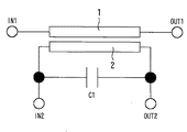
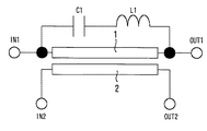
図1は、本発明の実施の形態1に係る方向性結合器を示す図である。主線路1が入力端子IN1と出力端子OUT1との間に接続されている。この主線路1は高周波信号を伝搬する。副線路2が入力端子IN2と出力端子OUT2との間に接続されている。この副線路2は、主線路1に対して平行に配置され、主線路1に電磁気的に結合されている。
FIG. 1 is a diagram showing a directional coupler according to
本実施の形態では、副線路2に対して並列にキャパシタC1が接続されている。主線路1及び副線路2が持つインダクタンスLとキャパシタC1が持つキャパシタンスCによりLC共振回路が構成される。このLC共振回路は、入力端子IN1から出力端子OUT2に伝搬する高周波信号に対して共振する。入力端子IN1から出力端子OUT2に伝搬する高周波信号の周波数をfとすると、キャパシタンスCはf=1/2π(LC)1/2のLC共振の関係を満たす値に設定されている。また、LC共振回路の共振のピークの鋭さ表すQ値は、LC共振回路の抵抗値R、インダクタンスL、キャパシタンスCを用いてQ=(L/C)1/2/Rで与えられる。
In the present embodiment, a capacitor C1 is connected in parallel to the
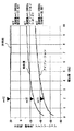
図2は、本発明の実施の形態1に係る方向性結合器のSパラメータの計算結果を示す図である。S(2,1)は主線路1を伝播する高周波信号であり、周波数は約4.5GHzである。S(4,1)は主線路1の入力端子IN1から副線路2の出力端子OUT2に伝搬する高周波信号であり、周波数は約2GHzである。従って、本実施の形態では、LC共振回路が約2GHzで共振するようにキャパシタンスCが設定されている。
FIG. 2 is a diagram showing a calculation result of the S parameter of the directional coupler according to
続いて、本実施の形態の効果について比較例と比較して説明する。比較例は本実施の構成からキャパシタC1を省略したものである。図3は、本発明の実施の形態1に係る方向性結合器の方向性の計算結果を示す図である。図4は、比較例に係る方向性結合器の方向性の計算結果を示す図である。縦軸は方向性(directivity)、結合度(coupling)、アイソレーション(isolation)であり、横軸は周波数である。この計算結果より、実施の形態1では比較例に比べて、周波数1.95GHzを中心に1.1GHzから2.4GHzの周波数範囲で方向性が改善することが分かる。
Subsequently, the effect of the present embodiment will be described in comparison with a comparative example. In the comparative example, the capacitor C1 is omitted from the configuration of the present embodiment. FIG. 3 is a diagram illustrating a calculation result of the directionality of the directional coupler according to
比較例では、結合度を大きくするために線路間隔を小さくすると、偶奇モードの各位相速度に差が生じて方向性が劣化する。これに対して、本実施の形態では、キャパシタC1を設けて、そのキャパシタンスCを上記の共振条件を満たすように設定することで、大きな結合度を得ながら、良好な方向性も得ることができる。 In the comparative example, if the line spacing is reduced in order to increase the degree of coupling, a difference occurs in the phase speeds of the even and odd modes, and the directionality deteriorates. On the other hand, in this embodiment, by providing the capacitor C1 and setting the capacitance C so as to satisfy the above resonance condition, it is possible to obtain a good directionality while obtaining a large degree of coupling. .
ここで、位相速度はLやCに依存(1/(LC)1/2に比例)するので、LやCを変えることで位相速度を調整できる。そして、方向性が改善する周波数では、偶奇モードの位相速度が一致していると推測される。従って、本実施の形態では、LC共振により偶奇モードの位相速度の差を補償できると考えられる。 Here, since the phase velocity depends on L and C (proportional to 1 / (LC) 1/2 ), the phase velocity can be adjusted by changing L and C. Then, it is presumed that the phase speeds of the even and odd modes match at the frequency where the directionality is improved. Therefore, in the present embodiment, it is considered that the phase speed difference in the even / odd mode can be compensated by LC resonance.
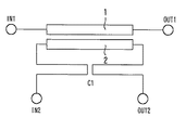
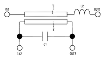
図5は、本発明の実施の形態1に係る方向性結合器の変形例1を示す図である。キャパシタC1が主線路1に対して並列に接続されている点が実施の形態1とは異なる。この場合でも、入力端子IN1から出力端子OUT2に伝搬する高周波信号に対してLC共振回路が共振する条件を満たす限り、実施の形態1と同様の効果を得ることができる。
FIG. 5 is a diagram showing a first modification of the directional coupler according to
図6は、本発明の実施の形態1に係る方向性結合器の変形例2を示す図である。主線路1の幅に対して副線路2の幅を狭くする。これにより、方向性結合器を小型化することができる。また、もし仮に主線路1を狭くすると主線路1の損失が増加してしまうが、変形例2では主線路1の損失は増加しない。
FIG. 6 is a diagram illustrating a second modification of the directional coupler according to the first embodiment of the present invention. The width of the
図7は、本発明の実施の形態1に係る方向性結合器の変形例3を示す図である。このように線路間隔を狭くしてキャパシタC1を構成しても、同様の効果を得ることができる。
FIG. 7 is a diagram showing a third modification of the directional coupler according to
また、キャパシタC1としてMIM(Metal-Insulator-Metal)キャパシタを用いても、同様の効果を得ることができる。この場合、MIMキャパシタのサイズを小さくするために、キャパシタC1に対して直列に接続されたインダクタを付加してもよい。 The same effect can be obtained even if an MIM (Metal-Insulator-Metal) capacitor is used as the capacitor C1. In this case, an inductor connected in series with the capacitor C1 may be added to reduce the size of the MIM capacitor.
実施の形態2.
図8は、本発明の実施の形態2に係る方向性結合器を示す図である。実施の形態1の構成に、キャパシタC1に対して直列に接続された抵抗R1が付加されている。これにより、Q値を小さくし、方向性結合器とキャパシタC1のLC共振のピークを鈍らせることができる。従って、改善する方向性の周波数範囲を実施の形態1よりも広げることができる。
FIG. 8 is a diagram showing a directional coupler according to
図9は、本発明の実施の形態2に係る方向性結合器の変形例を示す図である。実施の形態1の変形例1の構成に、キャパシタC1に対して直列に接続された抵抗R1が付加されている。これにより実施の形態2と同様の効果を得ることができる。
FIG. 9 is a diagram showing a modification of the directional coupler according to
実施の形態3.
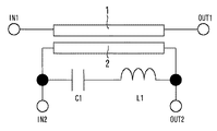
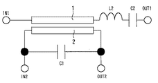
図10は、本発明の実施の形態3に係る方向性結合器を示す図である。実施の形態1の構成に、キャパシタC1に対して直列に接続されたインダクタL1が付加されている。これにより、Q値を大きくし、方向性結合器とキャパシタC1のLC共振のピークを鋭くすることができる。従って、実施の形態1と比較して、狭い周波数範囲で改善する方向性の絶対値を大きくすることができる。さらに、実施の形態1と比較して、キャパシタC1のキャパシタンスを小さくすることもできる。
FIG. 10 is a diagram showing a directional coupler according to
図11は、本発明の実施の形態3に係る方向性結合器の変形例を示す図である。実施の形態1の変形例1の構成に、キャパシタC1に対して直列に接続されたインダクタL1が付加されている。これにより実施の形態3と同様の効果を得ることができる。
FIG. 11 is a diagram showing a modification of the directional coupler according to
実施の形態4.
図12は、本発明の実施の形態4に係る方向性結合器を示す図である。実施の形態1の構成に、主線路1に対して直列に接続されたインダクタL2が付加されている。これにより、方向性結合器のインダクタンスを変えることができる。従って、実施の形態1と比較して、改善する方向性の周波数の中心値、周波数範囲、及び共振のピークの鋭さを調整することができる。
FIG. 12 is a diagram showing a directional coupler according to
図13は、本発明の実施の形態4に係る方向性結合器の変形例を示す図である。実施の形態1の変形例1の構成に、主線路1に対して直列に接続されたインダクタL2が付加されている。これにより実施の形態4と同様の効果を得ることができる。
FIG. 13 is a diagram showing a modification of the directional coupler according to
実施の形態5.
図14は、本発明の実施の形態5に係る方向性結合器を示す図である。実施の形態1の構成に、主線路1に対して直列に接続されたインダクタL2とキャパシタC2が付加されている。これにより、方向性結合器のインダクタンスとキャパシタンスを変えることができる。従って、実施の形態1と比較して、改善する方向性の周波数の中心値、周波数範囲、及び共振のピークの鋭さを調整することができる。
FIG. 14 is a diagram showing a directional coupler according to
図15は、本発明の実施の形態5に係る方向性結合器の変形例を示す図である。実施の形態1の変形例1の構成に、主線路1に対して直列に接続されたインダクタL2とキャパシタC2が付加されている。これにより実施の形態5と同様の効果を得ることができる。
FIG. 15 is a diagram showing a modification of the directional coupler according to
実施の形態6.
図16は、本発明の実施の形態6に係る方向性結合器を示す図である。実施の形態2の構成に、実施の形態4のインダクタL2が付加されている。これにより実施の形態2と実施の形態4の効果を得ることができる。即ち、方向性結合器のインダクタンスを変えてQ値を調整しながら、方向性の周波数範囲を広げることができる。
FIG. 16 is a diagram showing a directional coupler according to
例えば、狭い周波数範囲で改善する方向性の絶対値を大きくする場合は、Q値を大きくする必要があるので、キャパシタンスを小さくし、インダクタンスを大きくし、抵抗値を小さくすればよい。一方、広い周波数範囲で方向性を改善したい場合は、Q値を小さくする必要があるため、逆の調整をすればよい。ただし、LC共振回路の共振周波数の中心値が、方向性を改善する周波数の中心値と等しくなるようにする必要がある。 For example, when increasing the absolute value of directionality to be improved in a narrow frequency range, it is necessary to increase the Q value. Therefore, it is only necessary to decrease the capacitance, increase the inductance, and decrease the resistance value. On the other hand, when it is desired to improve the directivity in a wide frequency range, the Q value needs to be reduced, and therefore, the reverse adjustment may be performed. However, the center value of the resonance frequency of the LC resonance circuit needs to be equal to the center value of the frequency that improves the directionality.
図17は、本発明の実施の形態6に係る方向性結合器の変形例を示す図である。実施の形態2の変形例の構成に、実施の形態4のインダクタL2が付加されている。これにより実施の形態3の変形例と実施の形態4の効果を得ることができる。
FIG. 17 is a diagram showing a modification of the directional coupler according to
実施の形態7.
図18は、本発明の実施の形態7に係る方向性結合器を示す図である。実施の形態3の構成に、実施の形態4のインダクタL2が付加されている。これにより実施の形態3と実施の形態4の効果を得ることができる。
FIG. 18 is a diagram showing a directional coupler according to
図19は、本発明の実施の形態7に係る方向性結合器の変形例を示す図である。実施の形態3の変形例の構成に、実施の形態4のインダクタL2が付加されている。これにより実施の形態3の変形例と実施の形態4の効果を得ることができる。
FIG. 19 is a diagram showing a modification of the directional coupler according to
実施の形態8.
図20は、本発明の実施の形態8に係る方向性結合器を示す図である。実施の形態2の構成に、実施の形態5のインダクタL2とキャパシタC2が付加されている。これにより実施の形態2と実施の形態5の効果を得ることができる。
FIG. 20 is a diagram showing a directional coupler according to
図21は、本発明の実施の形態8に係る方向性結合器の変形例を示す図である。実施の形態2の変形例の構成に、実施の形態5のインダクタL2とキャパシタC2が付加されている。これにより実施の形態2の変形例と実施の形態5の効果を得ることができる。
FIG. 21 is a diagram showing a modification of the directional coupler according to
実施の形態9.
図22は、本発明の実施の形態9に係る方向性結合器を示す図である。実施の形態3の構成に、実施の形態5のインダクタL2とキャパシタC2が付加されている。これにより実施の形態3と実施の形態5の効果を得ることができる。
FIG. 22 is a diagram showing a directional coupler according to
図23は、本発明の実施の形態9に係る方向性結合器の変形例を示す図である。実施の形態3の変形例の構成に、実施の形態5のインダクタL2とキャパシタC2が付加されている。これにより実施の形態3の変形例と実施の形態5の効果を得ることができる。
FIG. 23 is a diagram showing a modification of the directional coupler according to
1 主線路
2 副線路
C1 キャパシタ(第1のキャパシタ)
C2 キャパシタ(第2のキャパシタ)
IN1 入力端子(第1の入力端子)
IN2 入力端子(第2の入力端子)
L1 インダクタ(第1のインダクタ)
L2 インダクタ(第2のインダクタ)
OUT1 出力端子(第1の出力端子)
OUT2 出力端子(第2の出力端子)
R1 抵抗
1
C2 capacitor (second capacitor)
IN1 input terminal (first input terminal)
IN2 input terminal (second input terminal)
L1 inductor (first inductor)
L2 inductor (second inductor)
OUT1 output terminal (first output terminal)
OUT2 output terminal (second output terminal)
R1 resistance
Claims (3)
第2の入力端子と第2の出力端子との間に接続され、前記主線路に対して平行に配置され、前記主線路に電磁気的に結合された副線路と、
前記主線路又は前記副線路に対して並列に接続された第1のキャパシタと、
前記第1のキャパシタに対して直列に接続された抵抗とを備え、
前記主線路及び前記副線路が持つインダクタンスと前記第1のキャパシタが持つキャパシタンスによりLC共振回路が構成され、
前記LC共振回路は、前記第1の入力端子から前記第2の出力端子に伝搬する高周波信号に対して共振することを特徴とする方向性結合器。 A main line connected between the first input terminal and the first output terminal for propagating a high-frequency signal;
A sub-line connected between the second input terminal and the second output terminal, arranged parallel to the main line, and electromagnetically coupled to the main line;
A first capacitor connected in parallel to the main line or the sub-line ;
A resistor connected in series with the first capacitor ;
An LC resonance circuit is configured by the inductance of the main line and the sub line and the capacitance of the first capacitor,
The LC resonant circuit resonates with a high-frequency signal propagating from the first input terminal to the second output terminal.
Priority Applications (5)
| Application Number | Priority Date | Filing Date | Title |
|---|---|---|---|
| JP2010253884A JP5609574B2 (en) | 2010-11-12 | 2010-11-12 | Directional coupler |
| US13/115,166 US8922295B2 (en) | 2010-11-12 | 2011-05-25 | Directional coupler |
| TW100118626A TWI479733B (en) | 2010-11-12 | 2011-05-27 | Directional coupler |
| CN201110246595.5A CN102468526B (en) | 2010-11-12 | 2011-08-24 | Directional coupler |
| KR1020110113709A KR101329611B1 (en) | 2010-11-12 | 2011-11-03 | Directional coupler |
Applications Claiming Priority (1)
| Application Number | Priority Date | Filing Date | Title |
|---|---|---|---|
| JP2010253884A JP5609574B2 (en) | 2010-11-12 | 2010-11-12 | Directional coupler |
Publications (3)
| Publication Number | Publication Date |
|---|---|
| JP2012105193A JP2012105193A (en) | 2012-05-31 |
| JP2012105193A5 JP2012105193A5 (en) | 2013-10-24 |
| JP5609574B2 true JP5609574B2 (en) | 2014-10-22 |
Family
ID=46047232
Family Applications (1)
| Application Number | Title | Priority Date | Filing Date |
|---|---|---|---|
| JP2010253884A Active JP5609574B2 (en) | 2010-11-12 | 2010-11-12 | Directional coupler |
Country Status (5)
| Country | Link |
|---|---|
| US (1) | US8922295B2 (en) |
| JP (1) | JP5609574B2 (en) |
| KR (1) | KR101329611B1 (en) |
| CN (1) | CN102468526B (en) |
| TW (1) | TWI479733B (en) |
Families Citing this family (11)
| Publication number | Priority date | Publication date | Assignee | Title |
|---|---|---|---|---|
| JP6230248B2 (en) * | 2013-03-29 | 2017-11-15 | 三菱電機株式会社 | Directional coupler |
| US9318788B2 (en) * | 2013-06-05 | 2016-04-19 | Telefonaktiebolaget Lm Ericsson (Publ) | Directional coupler |
| JP5786902B2 (en) * | 2013-06-26 | 2015-09-30 | 株式会社村田製作所 | Directional coupler |
| US20150042412A1 (en) * | 2013-08-07 | 2015-02-12 | Qualcomm Incorporated | Directional coupler circuit techniques |
| JP6112075B2 (en) * | 2014-06-27 | 2017-04-12 | 株式会社村田製作所 | Electronic components |
| WO2016121455A1 (en) * | 2015-01-29 | 2016-08-04 | 株式会社村田製作所 | High-frequency module |
| US10263315B2 (en) * | 2015-07-22 | 2019-04-16 | Kyocera Corporation | Directional coupler and communication module |
| EP3220477B1 (en) * | 2016-03-17 | 2018-08-15 | AKG Acoustics GmbH | Directional coupler and power splitter made therefrom |
| CN106207363A (en) * | 2016-08-30 | 2016-12-07 | 宇龙计算机通信科技(深圳)有限公司 | A kind of directional coupler |
| CN109845029B (en) | 2016-10-27 | 2021-03-09 | 株式会社村田制作所 | Substrate with built-in directional coupler, high-frequency front-end circuit, and communication device |
| KR102142520B1 (en) * | 2018-05-11 | 2020-08-07 | 삼성전기주식회사 | Coupler circuit with phase compensation function |
Family Cites Families (11)
| Publication number | Priority date | Publication date | Assignee | Title |
|---|---|---|---|---|
| JPS6173355A (en) * | 1984-09-19 | 1986-04-15 | Hitachi Ltd | Semiconductor device |
| JP3289643B2 (en) | 1997-04-11 | 2002-06-10 | 株式会社村田製作所 | Directional coupler |
| JP2000278168A (en) | 1999-03-25 | 2000-10-06 | Murata Mfg Co Ltd | High frequency composite component and radio communication unit using the same |
| JP2001094315A (en) | 1999-09-20 | 2001-04-06 | Hitachi Metals Ltd | Directional coupler |
| US6894578B1 (en) * | 2000-04-06 | 2005-05-17 | Hitachi Metals, Ltd. | Irreversible circuit module including a directional coupler |
| JP2002299922A (en) * | 2001-03-30 | 2002-10-11 | Kyocera Corp | High frequency module |
| US6683512B2 (en) * | 2001-06-21 | 2004-01-27 | Kyocera Corporation | High frequency module having a laminate board with a plurality of dielectric layers |
| JP2004289797A (en) | 2002-12-06 | 2004-10-14 | Stmicroelectronics Sa | Directional coupler |
| JP3832447B2 (en) * | 2003-04-16 | 2006-10-11 | 松下電器産業株式会社 | Distributor and high-frequency signal transmitter / receiver using the same |
| JP2005117497A (en) | 2003-10-09 | 2005-04-28 | Kyocera Corp | High-frequency module and radio communication device mounting same |
| JP5049886B2 (en) * | 2008-06-06 | 2012-10-17 | 双信電機株式会社 | High frequency switch |
-
2010
- 2010-11-12 JP JP2010253884A patent/JP5609574B2/en active Active
-
2011
- 2011-05-25 US US13/115,166 patent/US8922295B2/en active Active
- 2011-05-27 TW TW100118626A patent/TWI479733B/en active
- 2011-08-24 CN CN201110246595.5A patent/CN102468526B/en active Active
- 2011-11-03 KR KR1020110113709A patent/KR101329611B1/en active IP Right Grant
Also Published As
| Publication number | Publication date |
|---|---|
| CN102468526B (en) | 2014-11-05 |
| JP2012105193A (en) | 2012-05-31 |
| US8922295B2 (en) | 2014-12-30 |
| TW201220593A (en) | 2012-05-16 |
| TWI479733B (en) | 2015-04-01 |
| US20120119846A1 (en) | 2012-05-17 |
| CN102468526A (en) | 2012-05-23 |
| KR101329611B1 (en) | 2013-11-15 |
| KR20120051580A (en) | 2012-05-22 |
Similar Documents
| Publication | Publication Date | Title |
|---|---|---|
| JP5609574B2 (en) | Directional coupler | |
| US8305283B2 (en) | Coplanar differential bi-strip delay line, higher-order differential filter and filtering antenna furnished with such a line | |
| US20160218695A1 (en) | Ladder filter | |
| JP6308221B2 (en) | Variable frequency filter | |
| US20160164487A1 (en) | Bulk acoustic wave filter | |
| JP4629571B2 (en) | Microwave circuit | |
| CN106911317A (en) | SAW resonator | |
| WO2015052838A1 (en) | Decoupling circuit | |
| TWI723648B (en) | Noise suppression filter and method for manufacturing a noise suppression filter | |
| US20150137907A1 (en) | Directional coupler having high isolation | |
| JP6262437B2 (en) | Polarized bandpass filter | |
| US11088669B2 (en) | Band pass filter | |
| JP3864974B2 (en) | Dielectric filter, dielectric duplexer, and communication device | |
| JP2008079027A (en) | High frequency delay line | |
| EP2790266B1 (en) | Filter and resonator | |
| JP5261258B2 (en) | Bandpass filter | |
| KR100471017B1 (en) | Circuit for Generating Complementary Ripple Having Asymmetrical Shape with Unicorn Type | |
| JP2008054174A (en) | 90-degree hybrid circuit | |
| US11063569B2 (en) | Common mode noise suppression filter | |
| KR101919704B1 (en) | Low loss matching circuit for power amplifier using resonance structure | |
| JP2008187459A (en) | Rat-race hybrid | |
| JP6532618B2 (en) | High frequency circuit and high frequency power amplifier | |
| WO2019235490A1 (en) | Multiplexer | |
| CN117525797A (en) | Filtering power divider with high isolation | |
| JP2009260639A (en) | High frequency amplifier |
Legal Events
| Date | Code | Title | Description |
|---|---|---|---|
| A521 | Written amendment |
Free format text: JAPANESE INTERMEDIATE CODE: A523 Effective date: 20130909 |
|
| A621 | Written request for application examination |
Free format text: JAPANESE INTERMEDIATE CODE: A621 Effective date: 20130909 |
|
| A977 | Report on retrieval |
Free format text: JAPANESE INTERMEDIATE CODE: A971007 Effective date: 20140227 |
|
| A131 | Notification of reasons for refusal |
Free format text: JAPANESE INTERMEDIATE CODE: A131 Effective date: 20140304 |
|
| A521 | Written amendment |
Free format text: JAPANESE INTERMEDIATE CODE: A523 Effective date: 20140319 |
|
| TRDD | Decision of grant or rejection written | ||
| A01 | Written decision to grant a patent or to grant a registration (utility model) |
Free format text: JAPANESE INTERMEDIATE CODE: A01 Effective date: 20140805 |
|
| A61 | First payment of annual fees (during grant procedure) |
Free format text: JAPANESE INTERMEDIATE CODE: A61 Effective date: 20140818 |
|
| R150 | Certificate of patent or registration of utility model |
Ref document number: 5609574 Country of ref document: JP Free format text: JAPANESE INTERMEDIATE CODE: R150 |
|
| R250 | Receipt of annual fees |
Free format text: JAPANESE INTERMEDIATE CODE: R250 |
|
| R250 | Receipt of annual fees |
Free format text: JAPANESE INTERMEDIATE CODE: R250 |
|
| S111 | Request for change of ownership or part of ownership |
Free format text: JAPANESE INTERMEDIATE CODE: R313113 |
|
| R350 | Written notification of registration of transfer |
Free format text: JAPANESE INTERMEDIATE CODE: R350 |