JP5605729B2 - Conductive device surrounded by insulating material and method for electrically shielding voltage structure - Google Patents
Conductive device surrounded by insulating material and method for electrically shielding voltage structure Download PDFInfo
- Publication number
- JP5605729B2 JP5605729B2 JP2010521991A JP2010521991A JP5605729B2 JP 5605729 B2 JP5605729 B2 JP 5605729B2 JP 2010521991 A JP2010521991 A JP 2010521991A JP 2010521991 A JP2010521991 A JP 2010521991A JP 5605729 B2 JP5605729 B2 JP 5605729B2
- Authority
- JP
- Japan
- Prior art keywords
- conductor
- insulating
- conductive device
- segments
- insulating material
- Prior art date
- Legal status (The legal status is an assumption and is not a legal conclusion. Google has not performed a legal analysis and makes no representation as to the accuracy of the status listed.)
- Active
Links
Images


Classifications
-
- H—ELECTRICITY
- H01—ELECTRIC ELEMENTS
- H01J—ELECTRIC DISCHARGE TUBES OR DISCHARGE LAMPS
- H01J37/00—Discharge tubes with provision for introducing objects or material to be exposed to the discharge, e.g. for the purpose of examination or processing thereof
- H01J37/30—Electron-beam or ion-beam tubes for localised treatment of objects
- H01J37/317—Electron-beam or ion-beam tubes for localised treatment of objects for changing properties of the objects or for applying thin layers thereon, e.g. for ion implantation
- H01J37/3171—Electron-beam or ion-beam tubes for localised treatment of objects for changing properties of the objects or for applying thin layers thereon, e.g. for ion implantation for ion implantation
-
- H—ELECTRICITY
- H01—ELECTRIC ELEMENTS
- H01B—CABLES; CONDUCTORS; INSULATORS; SELECTION OF MATERIALS FOR THEIR CONDUCTIVE, INSULATING OR DIELECTRIC PROPERTIES
- H01B17/00—Insulators or insulating bodies characterised by their form
- H01B17/56—Insulating bodies
-
- H—ELECTRICITY
- H01—ELECTRIC ELEMENTS
- H01J—ELECTRIC DISCHARGE TUBES OR DISCHARGE LAMPS
- H01J37/00—Discharge tubes with provision for introducing objects or material to be exposed to the discharge, e.g. for the purpose of examination or processing thereof
- H01J37/02—Details
- H01J37/04—Arrangements of electrodes and associated parts for generating or controlling the discharge, e.g. electron-optical arrangement, ion-optical arrangement
- H01J37/09—Diaphragms; Shields associated with electron or ion-optical arrangements; Compensation of disturbing fields
-
- H—ELECTRICITY
- H01—ELECTRIC ELEMENTS
- H01J—ELECTRIC DISCHARGE TUBES OR DISCHARGE LAMPS
- H01J37/00—Discharge tubes with provision for introducing objects or material to be exposed to the discharge, e.g. for the purpose of examination or processing thereof
- H01J37/30—Electron-beam or ion-beam tubes for localised treatment of objects
- H01J37/317—Electron-beam or ion-beam tubes for localised treatment of objects for changing properties of the objects or for applying thin layers thereon, e.g. for ion implantation
-
- H—ELECTRICITY
- H01—ELECTRIC ELEMENTS
- H01J—ELECTRIC DISCHARGE TUBES OR DISCHARGE LAMPS
- H01J2237/00—Discharge tubes exposing object to beam, e.g. for analysis treatment, etching, imaging
- H01J2237/20—Positioning, supporting, modifying or maintaining the physical state of objects being observed or treated
- H01J2237/2001—Maintaining constant desired temperature
-
- H—ELECTRICITY
- H01—ELECTRIC ELEMENTS
- H01J—ELECTRIC DISCHARGE TUBES OR DISCHARGE LAMPS
- H01J2237/00—Discharge tubes exposing object to beam, e.g. for analysis treatment, etching, imaging
- H01J2237/26—Electron or ion microscopes
Landscapes
- Chemical & Material Sciences (AREA)
- Analytical Chemistry (AREA)
- Insulated Conductors (AREA)
- Cable Accessories (AREA)
- Insulators (AREA)
- Insulation, Fastening Of Motor, Generator Windings (AREA)
- Transformers For Measuring Instruments (AREA)
Description
本開示は概して、電界応力の遮蔽に関する。特に、電圧構造を電気的に遮蔽するための絶縁導電デバイスに関する。 The present disclosure relates generally to field stress shielding. In particular, it relates to an insulated conductive device for electrically shielding a voltage structure.
イオン注入は、導電性を変更する不純物を半導体ウェハに導入する、つまり、半導体ウェハに対してドーピングを行う際に標準的に利用されている技術である。通常のイオン注入処理では、半導体ウェハに不純物(イオン)を導入する際に、エネルギーが与えられているイオンビームを利用する。イオン注入では、原材料となる供給材料にエネルギーを与えてイオンビームを生成して、生成されたイオンビームを、例えば、670kVという高圧で加速コラムを用いて加速する必要がある。電圧構造(通常は、ターミナルと呼ばれる)を用いて、このような高圧を実現する。 Ion implantation is a technique that is used as a standard when introducing impurities that change conductivity into a semiconductor wafer, that is, when doping a semiconductor wafer. In a normal ion implantation process, an ion beam to which energy is applied is used when introducing impurities (ions) into a semiconductor wafer. In ion implantation, it is necessary to generate energy by supplying energy to a raw material, and to accelerate the generated ion beam using an acceleration column at a high pressure of 670 kV, for example. Such a high voltage is achieved using a voltage structure (usually called a terminal).
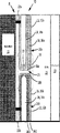
同時係属中の米国特許出願第11/527,842号(出願日:2006年9月27日)では、イオン注入装置において電圧構造のための電気応力遮蔽部として利用される絶縁導体が開示されている。当該米国出願は、参照により本願に組み込まれる。図1は、当該米国出願第11/527,842号に開示されている電圧構造400を示す斜視図である。図1を参照しつつ説明すると、電圧構造400は、底面と、ベースに結合されている1以上の直立側壁404と、1以上の直立側壁404に結合されている上面402とを備えるとしてよい。1つの直立側壁404は、ハンドル442が備えられたドア440を有するとしてよく、電圧構造400の内部空間へと人がアクセスできるようになっている。電圧構造400が備える1つの直立側壁404は、固体材料から成る1つの部材として製造されるとしてもよいし、または、任意の数の別個の部材として製造されるとしてもよい。電圧構造400の上面402は、固体部材として図示されているが、互いから離間されて複数の導体が設けられて一種の導体メッシュとして構成され、メッシュの開口部分から空気を流入させ得るとしてもよい。
Co-pending US patent application Ser. No. 11 / 527,842 (filing date: September 27, 2006) discloses an insulated conductor utilized as an electrical stress shield for voltage structures in an ion implanter. Yes. That US application is incorporated herein by reference. FIG. 1 is a perspective view showing a voltage structure 400 disclosed in the US application Ser. No. 11 / 527,842. Referring to FIG. 1, the voltage structure 400 may include a bottom surface, one or more
電圧構造400の外面のうち電気応力が過剰である部分の近傍に、1以上の絶縁導体412が設けられているとしてよい。図1において、上部絶縁導体412は、電圧構造400の上側端縁470の近傍に全周にわたって設けられており、下部絶縁導体412は、下側端縁472の近傍に全周にわたって設けられている。上部絶縁導体412および下部絶縁導体412は端縁470および472の全周の近傍に配置されているが、別の実施形態では、これに加えて、または、これに代えて、外面の別の部分に絶縁導体412を配設するとしてよい。そのような部分としては、これらに限定されないが、水平端縁、垂直端縁、角、および、電圧構造400と外部部品とがインターフェースしている箇所である開口または界面等が挙げられる。外部部品には、モーター、生成器、または系統連系が含まれるとしてよい。一例を挙げると、球状の形状を持つ絶縁導体が、電圧構造400の角の近傍に配置されるとしてよい。絶縁導体412は、例えば、75kV/インチを超える絶縁耐力を持つ絶縁体416を含むとしてよい。
One or more
複数のブラケット422は、電圧構造400および対応する絶縁導体412に結合されており、電圧構造400の外側部分の近傍に配置されている絶縁導体412を支持している。ブラケット422の長さは、絶縁導体412を電圧構造400から所望の距離だけ離して配置できるような長さであるとしてよい。所望の距離の範囲は、実質的にゼロ(実質的に接触している状態)から周囲の空隙が許容する最大距離までとしてよい。一実施形態によると、所望の距離は少なくとも1.5インチである。ブラケット422の形成材料は、導電材料であってもよいし、または、非導電材料であってもよい。また、ブラケット422は、電圧構造400と絶縁導体412との間を電気接続する機能を持つとしてもよい。
The plurality of
図1に示すように、絶縁導体412および絶縁体416はそれぞれ、閉じた状態の連続している一体成形部材として構成されている。一体成形部材として構成される絶縁体416のサイズが大きいので、製造、設置、メインテナンス、コスト、および信頼性において問題が発生する場合がある。
As shown in FIG. 1, the
本開示の第1の側面によると、電圧構造のための絶縁導電デバイスが提供される。当該絶縁導電デバイスは、電圧に接続されている導体と、導体が内部に封入されている複数の絶縁セグメントとを備え、複数の絶縁セグメントは、互いにインターフェースしている。 According to a first aspect of the present disclosure, an insulated conductive device for a voltage structure is provided. The insulated conductive device includes a conductor connected to a voltage and a plurality of insulating segments in which the conductor is enclosed, and the plurality of insulating segments interface with each other.
本開示の第2の側面によると、電圧構造のための絶縁導電デバイスが提供される。当該絶縁導電デバイスは、互いにインターフェースしており、それぞれが絶縁部分の内部に封入されている導体を有する複数のセグメントを備え、導体は、複数の導体ケーブルを含み、複数の導体ケーブルのうち1つは電圧構造に接続されている。 According to a second aspect of the present disclosure, an insulated conductive device for a voltage structure is provided. The insulated conductive device includes a plurality of segments that interface with each other, each having a conductor encapsulated within an insulated portion, the conductor including a plurality of conductor cables, and one of the plurality of conductor cables. Is connected to the voltage structure.
本開示の第3の側面によると、電圧構造を電気的に遮蔽する方法が提供される。当該方法は、誘電材料によって包み込まれている導体を有するセグメントを複数用意する段階と、それぞれの導体を電圧構造に接続する段階と、直接隣接する2つの導体の等電位線が一の連続導体の等電位線と実質的に同様になるように直接隣接する2つの導体を近接して配置するように、複数のセグメントを配置する段階とを備える。 According to a third aspect of the present disclosure, a method for electrically shielding a voltage structure is provided. The method includes the steps of providing a plurality of segments having conductors encased in a dielectric material, connecting each conductor to a voltage structure, and having a continuous conductor with one equipotential line between two adjacent conductors. Arranging a plurality of segments such that two conductors that are directly adjacent to each other are arranged close to each other so as to be substantially similar to an equipotential line.
上記に例示した本開示の側面は、本明細書に記載した問題および/または本明細書には記載しないその他の問題を解決するためのものである。 The aspects of the present disclosure illustrated above are intended to solve the problems described herein and / or other problems not described herein.
本開示の上述した特徴およびその他の特徴は、以下に記載する本開示のさまざまな側面の詳細な説明を添付図面と共に参照することによってより容易に明らかとなる。添付図面では、本開示のさまざまな実施形態を図示している。添付図面は以下の通りである。 The foregoing and other features of the present disclosure will become more readily apparent by reference to the following detailed description of various aspects of the present disclosure, taken in conjunction with the accompanying drawings. The accompanying drawings illustrate various embodiments of the present disclosure. The attached drawings are as follows.
尚、本開示を示す図面は実寸には即していないことに留意されたい。添付図面は、本開示の一般的な側面のみを図示することを意図しているので、本開示の範囲を制限するものと解釈されるべきではない。図面において、同様の参照番号は、複数の図面にわたって、同様の構成要素を表すものとする。 It should be noted that the drawings illustrating the present disclosure are not to scale. The accompanying drawings are intended to illustrate only the general aspects of the present disclosure and should not be construed to limit the scope of the present disclosure. In the drawings, like reference numbers represent like elements throughout the several views.
図面を参照しつつ説明する。図2は、一実施形態に係る絶縁導電デバイス10を示す概略図である。図2に示すように、システム8は、電圧構造11および絶縁導電デバイス10を備える。絶縁導電デバイス10は、電圧構造11とグラウンド13との間に配置されている。グラウンド13は、例えば、金属構造である。絶縁導電デバイス10とグラウンド13との間の間隙には、空気15が充填されている。絶縁導電デバイス10は、複数のセグメント12(例として、12a、12bが図示されている)を有しており、各セグメント12は、導体セグメント14(例として、14a、14bが図示されている)および絶縁セグメント16(例として、16a、16bが図示されている)を含む。絶縁セグメント16は、例えば、塩素化ポリ塩化ビニル(CPVC)、シリコーン・シンタクチック・フォーム、エポキシ樹脂等の誘電材料から形成されるとしてよい。セグメント12bにのみ図示しているが、絶縁セグメント16(16b)は、絶縁セグメント16の内部および絶縁セグメント16の周囲の空気15における径方向応力を制御することを目的として、複数の異なる材料からなる複数の層161、162から形成されているとしてもよい。導体セグメント14は、対応する絶縁セグメント16によって包み込まれており、つまり、対応する絶縁セグメント16の内部に封入されている。
This will be described with reference to the drawings. FIG. 2 is a schematic diagram illustrating an insulated
互いに直接隣接する2つの絶縁セグメント16a、16bは、互いにインターフェースしている。本明細書において、「インターフェース」という用語は、2つの絶縁セグメント16a、16bが互いに対して近接して配置されていることを意味しており、これに限定されないが、絶縁セグメント16a、16bが互いに接触していることを含む。ある実施形態によると、互いにインターフェースする2つの絶縁セグメント16a、16bの間には、特に、インターフェース領域21における絶縁強度を改善することを目的として、インターフェース媒体20が塗布されているとしてよい。ある実施形態によると、インターフェース媒体20は、インターフェース領域21を超えて広がり、絶縁セグメント16a、16bの一部を被覆している。
Two insulating segments 16a, 16b directly adjacent to each other interface with each other. In this specification, the term “interface” means that two insulating segments 16a, 16b are arranged in close proximity to each other, but not limited thereto, the insulating segments 16a, 16b are connected to each other. Including contact. According to an embodiment, an
図2では導体セグメント14a、14bはそれぞれ、対応する接続ビア22a、22bを介して個別に電圧構造11に接続されているが、必ずしもこのような構成でなくてもよい。例えば、別の実施形態によると、導体セグメント14a、14bは、導体セグメント14a、14bの電位を実質的に等しく維持する限りにおいて、電圧構造11とは別の電源に個別に接続されているとしてもよい。例えば、導体セグメント14a、14bは、例えば670kVである電圧構造11とは異なる電位、例えば500kVに接続されているとしてもよい。500kVにおいても、絶縁導電デバイス10は電圧構造11を遮蔽し、グラウンド13と絶縁導電デバイス10との間の応力は低減される。
In FIG. 2, the conductor segments 14a and 14b are individually connected to the
ある実施形態によると、図3に示すように、導体セグメント14a、14bの等電位線24が、連続導体の等電位線、つまり、導体セグメント14a、14bが一体成形されている単一の導体である場合に見られる等電位線と実質的に同様となるように、導体セグメント14a、14bを互いに近接させる。また、等電位線24は、電圧構造11の電気応力を主に、電圧構造11の周囲の空気15に分散する代わりに、インターフェース媒体20および/または絶縁セグメント16a、16bの絶縁材料に分散する。この結果、絶縁破壊の発生が回避され得る。絶縁導電デバイス10の機能は、米国特許出願第11/527,842号に詳細に記載されている。
According to one embodiment, as shown in FIG. 3, the
ある実施形態によると、図2に示すように、絶縁セグメント16a、16bのインターフェース面18a、18bは、隣接面、例えば、26a、26bに対して実質的に垂直である。導体セグメント14の端縁27(14aにのみ図示)は、インターフェース面18aに対して実質的に丸みを帯びた形状となっている。
According to certain embodiments, as shown in FIG. 2, the
別の実施形態によると、図4に示すように、インターフェース面118aまたは118bは、隣接面126aまたは126bに対して、実質的に傾斜している。この場合、インターフェース面118a、118bは、互いに重なり合う。ある実施形態によると、図4に示すように、インターフェース面118aに隣接する導体セグメント14aの端縁128aもまた、実質的に傾斜している。傾斜している端縁128aは傾斜しているインターフェース面118aと一致していることが好ましく、つまり、端縁128aおよびインターフェース面118aは、同様の角度で傾斜している。ある実施形態によると、図2および図4に示すように、各導体セグメント14a、14bは、単一の中空金属パイプ(詳細な内容は不図示)であってよい。別の実施形態によると、図5Aに示すように、導体セグメント214は、複数の導体ケーブル215から成る導体ケーブル群を含むとしてよい。導体ケーブル215は、ケーブルを意味し、中心導体が絶縁材料内に閉じ込められている高圧ケーブルであることが好ましい。
According to another embodiment, as shown in FIG. 4, the
図5Aおよび図5Bを参照しつつ説明すると、セグメント212(例えば、図5Aおよび図5Bではそれぞれ212a、212bと図示)はそれぞれ、複数の導体ケーブル215(分かり易さのために、図5Aの左側にのみ図示)から成る導体ケーブル群を含む導体セグメント214を有する。ある実施形態によると、導体ケーブル群215は、複数の導体ケーブルを含み、例えば、4つの導体ケーブル215(1)、215(2)、215(3)、および、215(4)を含む。4つの導体ケーブル215のうち1つ、ここでは導体ケーブル215(4)は、接続ビア222を介して、電圧構造11に電気接続されている。接続ビア222は、接続ケーブル215(4)の一部として一体的に形成されるとしてもよい。
Referring to FIGS. 5A and 5B, the segments 212 (eg, 212a and 212b, respectively, shown in FIGS. 5A and 5B) each have a plurality of conductor cables 215 (on the left side of FIG. 5A for clarity). A conductor segment 214 including a conductor cable group consisting only of According to an embodiment, the
導体セグメント214はさらに、インターフェース面218(218a、218bと図示)に隣接している遮蔽導体部分236(セグメント212a、212bの236a、236bと図示)を含む。遮蔽導体部分236は、導体ケーブル群215よりも、インターフェース面218の近くまで延伸している。導体ケーブル群215は、遮蔽導体部分236の開口部分238(238a、238bと図示)内へと延伸することによって、遮蔽導体部分236と電気的に接続されている。
Conductor segment 214 further includes a shield conductor portion 236 (shown as 236a, 236b of segments 212a, 212b) adjacent to interface surface 218 (shown as 218a, 218b). The shield conductor portion 236 extends closer to the interface surface 218 than the
ある実施形態によると、遮蔽導体部分236は、図5Aの断面図の遮蔽導体部分236aが示しているように、実質的にU字形状に構成されており、U字形の接続端縁240はインターフェース面218aに面している。接続端縁240は、インターフェース面218aに対して丸みを帯びた形状となっている。ある実施形態によると、U字形の開口部分238aに隣接する端部242もまた、丸みを帯びた形状となっている。
According to one embodiment, the shield conductor portion 236 is configured in a substantially U shape, as shown by the shield conductor portion 236a in the cross-sectional view of FIG. 5A, and the
別の実施形態によると、遮蔽導体部分236は、図5Bの断面図に示す遮蔽導体部分236bのように、実質的にH字形状に構成されており、H字形の開口部分244はインターフェース面218bに面している。開口部分244に隣接する端部246は、インターフェース面218bに対して丸みを帯びた形状となっている。ある実施形態によると、H字形の開口部分238bに隣接する端部248もまた、丸みを帯びた形状である。
According to another embodiment, the shield conductor portion 236 is configured in a substantially H shape, such as the shield conductor portion 236b shown in the cross-sectional view of FIG. 5B, with the H-shaped
遮蔽導体部分236については、上記以外の物理的構造を持つことも可能であり、それらも本開示の範囲に含まれる。 The shielding conductor portion 236 may have a physical structure other than those described above, and these are included in the scope of the present disclosure.
さらに図5Aおよび図5Bを参照しつつ説明すると、セグメント212は、管状部分230および接続金型部分232を含む絶縁セグメント216(図示を簡潔にするべく図5Aにのみ図示)を有するとしてよい。ある実施形態によると、接続金型部分232は、インターフェース面218を含むとしてよい。管状部分230は、塩素化ポリ塩化ビニル(CPVC)から形成されるパイプを含むとしてよい。管状部分230は、図5Aおよび図5Bに示すように1つのパイプを含むとしてもよいし、または、図5Cに示すように、絶縁領域を複数の別個の/異なる空間235、237に分割するべく、複数の入れ子状のパイプ231、233を含むとしてもよい。尚、互いに異なる空間235、237は、互いに異なる絶縁材料(不図示)を含むとしてもよい。
Still referring to FIGS. 5A and 5B, the segment 212 may have an insulating segment 216 (shown only in FIG. 5A for simplicity of illustration) including a
導体ケーブル215は、図5Aおよび図5Bに示すように、実質的に直線であってもよいし、または、電気応力をさらに低減するべく、図5Dに示すようにコイル内蔵型管状部分230であってもよい。また、2つの導体ケーブル215は互いに位置を入れ替えるとしてもよく、例えば、相対的な位置を変えるとしてもよいし、または、管状部分230内で共にねじられた形状に構成されるとしてもよい。
The
図5Aに戻って、接続金型部分232は、セグメント212のインターフェース面218に隣接している。接続金型部分232の一部分234は、接続金型部分232と管状部分230とが結合されるように、管状部分230内に挿入/延伸させるとしてよい。接続金型部分232は実質的に、遮蔽導体部分236のうちケーブル215に接続されている一部分248を除いて、遮蔽導体部分236を包み込んでいる。接続金型部分232は、実質的に固相の非導電材料、たとえば、エポキシ樹脂(プラスチック)であってよい。
Returning to FIG. 5A, the connecting
ある実施形態によると、図5Aに示すように、接続金型部分232は遮蔽導体部分236の一部分248まで延伸する中空部分250を含むことが好ましい。導体ケーブル群215は、中空部分250を貫通して、遮蔽導体部分236に接続される。
According to certain embodiments, the connecting
別の実施形態によると、図6に示すように、絶縁導体デバイス312は、連続導体314および複数の絶縁セグメント316(316a、316bとして図示)を有する。連続導体314は、複数の導体ケーブル315を含み、そのうち1つの導体ケーブル315は電圧構造11に接続されるとしてよい。複数の絶縁セグメント316は、互いにインターフェースしており、全部で連続導体314を包み込んでいる。ある実施形態によると、絶縁セグメント316は、例えば、塩素化ポリ塩化ビニル(CPVC)製の絶縁パイプ338を含むとしてよい。連続導体314と絶縁パイプ338との間には、例えば、圧搾空気、SF6、シリコーン・シンタクチック・フォーム、または、エポキシ樹脂から成る別の絶縁層340が設けられるとしてよい。
According to another embodiment, the
別の実施形態によると、本開示はさらに、電圧構造、例えば、電圧構造11を電気的に遮蔽する方法を含む。具体的には、図2および図4から図6に示す絶縁導電デバイスを設けて、絶縁導体デバイスと電圧構造とを結合(配置)する。
According to another embodiment, the present disclosure further includes a method for electrically shielding a voltage structure, eg,
本開示によって、絶縁セグメントを有する絶縁導電デバイスの構造および関連する絶縁導電デバイス製造方法が提供されることが明らかである。本開示を好ましい実施形態に基づき具体的に図示および説明したが、当業者であれば、本開示の範囲を逸脱することなく、変更および修正を行えるものと考えられたい。 It is clear that the present disclosure provides a structure of an insulated conductive device having an insulated segment and an associated insulated conductive device manufacturing method. Although the present disclosure has been specifically illustrated and described based on preferred embodiments, it should be understood by those skilled in the art that changes and modifications can be made without departing from the scope of the present disclosure.
Claims (27)
前記導体が内部に封入されている複数の絶縁セグメントと
を備え、
前記複数の絶縁セグメントは、互いにインターフェースしている
前記電圧構造の外部に設けられた、絶縁材料に囲まれた導電デバイス。 A conductor connected to a voltage different from the voltage of the voltage structure ;
A plurality of insulating segments in which the conductor is enclosed, and
The plurality of insulating segments interface with each other
It provided outside of said voltage structure, the conductive device surrounded by an insulating material.
前記導体が内部に封入されている複数の絶縁セグメントとA plurality of insulating segments in which the conductor is enclosed;
を備え、With
前記複数の絶縁セグメントは、互いにインターフェースしているThe plurality of insulating segments interface with each other
電圧構造の外部に設けられた、絶縁材料に囲まれた導電デバイス。A conductive device surrounded by an insulating material provided outside the voltage structure.
前記導体が内部に封入されている複数の絶縁セグメントと
を備え、
前記複数の絶縁セグメントは、互いにインターフェースしており、
前記複数の絶縁セグメントのうち一の絶縁セグメントは、複数の異なる絶縁材料から形成される複数の層を有する
電圧構造の外部に設けられた、絶縁材料に囲まれた導電デバイス。 A conductor connected to the voltage;
A plurality of insulating segments in which the conductor is enclosed;
With
The plurality of insulating segments interface with each other;
A conductive device surrounded by an insulating material, wherein one insulating segment of the plurality of insulating segments is provided outside a voltage structure having a plurality of layers formed of a plurality of different insulating materials .
前記隣接面に対して傾斜しているか、
の一方である請求項6に記載の絶縁材料に囲まれた導電デバイス。 The interface surface of the insulating segment is perpendicular to the adjacent surface of the insulating segment, or
Is inclined with respect to the adjacent surface,
A conductive device surrounded by an insulating material according to claim 6 .
U字形状を持ち、前記U字形状の接続端縁は前記インターフェース面に対して丸みを帯びた形状となっているか、または、
H字形状を持ち、前記H字形状の開口部分は前記インターフェース面に面しており、隣接する前記H字形状の端部は、前記インターフェース面に対して丸みを帯びた形状となっているか、
のうち一方である請求項12に記載の絶縁材料に囲まれた導電デバイス。 In cross section, the shielding conductor portion is
Having a U-shape, and the U-shaped connection edge is rounded with respect to the interface surface, or
The H-shaped opening portion faces the interface surface, and the adjacent H-shaped end portion is rounded with respect to the interface surface;
A conductive device surrounded by an insulating material according to claim 12 , wherein the conductive device is one of the above.
互いにインターフェースしており、それぞれが絶縁部分の内部に封入されている導体を有するセグメントを複数備え、
前記導体は、複数の導体ケーブルを含み、前記複数の導体ケーブルのうち1つは前記電圧構造に接続されている
絶縁材料に囲まれた導電デバイス。 An electrically conductive device surrounded by an insulating material provided outside the voltage structure,
Comprising a plurality of segments having conductors that interface with each other, each encapsulated within an insulating portion;
The conductor includes a plurality of conductor cables, and one of the plurality of conductor cables is connected to the voltage structure. A conductive device surrounded by an insulating material.
前記導体は、前記インターフェース面に隣接する遮蔽導体部分を含み、
前記遮蔽導体部分の端縁は、前記インターフェース面に対して丸みを帯びた形状となっている
請求項22に記載の絶縁材料に囲まれた導電デバイス。 The insulating portion includes a chlorinated polyvinyl chloride (CPVC) pipe and a connecting mold portion adjacent to the interface surface of the segment;
The conductor includes a shielding conductor portion adjacent to the interface surface;
The conductive device surrounded by an insulating material according to claim 22 , wherein an edge of the shielding conductor portion has a rounded shape with respect to the interface surface.
誘電材料によって包み込まれている導体を有する複数の絶縁セグメントを用意する段階と、
それぞれの前記導体を前記電圧構造の電圧とは異なる電圧に接続する段階と、
前記複数の絶縁セグメントを互いにインターフェースするように配置する段階と
を備える方法。 A method of electrically shielding the voltage structure by providing a conductive device surrounded by an insulating material outside the voltage structure,
Providing a plurality of insulating segments having a conductor encased by a dielectric material;
Connecting each of said conductors to a voltage different from the voltage of said voltage structure;
Arranging the plurality of insulating segments to interface with each other .
誘電材料によって包み込まれている導体を有する複数の絶縁セグメントを用意する段階と、Providing a plurality of insulating segments having a conductor encased by a dielectric material;
一の連続導体であるそれぞれの前記導体を電圧に接続する段階とConnecting each said conductor, which is one continuous conductor, to a voltage;
前記複数の絶縁セグメントを互いにインターフェースするように配置する段階とDisposing the plurality of insulating segments to interface with each other;
を備える方法。A method comprising:
誘電材料によって包み込まれている導体を有する複数の絶縁セグメントを用意する段階と、Providing a plurality of insulating segments having a conductor encased by a dielectric material;
それぞれの前記導体を電圧に接続する段階とConnecting each said conductor to a voltage;
前記複数の絶縁セグメントを互いにインターフェースするように配置する段階とDisposing the plurality of insulating segments to interface with each other;
を備え、With
前記複数の絶縁セグメントのうち一の絶縁セグメントは、複数の異なる絶縁材料から形成される複数の層を有する方法。One insulating segment of the plurality of insulating segments having a plurality of layers formed from a plurality of different insulating materials.
Applications Claiming Priority (3)
| Application Number | Priority Date | Filing Date | Title |
|---|---|---|---|
| US11/841,086 US7799999B2 (en) | 2007-08-20 | 2007-08-20 | Insulated conducting device with multiple insulation segments |
| US11/841,086 | 2007-08-20 | ||
| PCT/US2008/073674 WO2009026340A2 (en) | 2007-08-20 | 2008-08-20 | Insulated conducting device with multiple insulation segments |
Publications (3)
| Publication Number | Publication Date |
|---|---|
| JP2010537386A JP2010537386A (en) | 2010-12-02 |
| JP2010537386A5 JP2010537386A5 (en) | 2011-08-25 |
| JP5605729B2 true JP5605729B2 (en) | 2014-10-15 |
Family
ID=40378967
Family Applications (1)
| Application Number | Title | Priority Date | Filing Date |
|---|---|---|---|
| JP2010521991A Active JP5605729B2 (en) | 2007-08-20 | 2008-08-20 | Conductive device surrounded by insulating material and method for electrically shielding voltage structure |
Country Status (6)
| Country | Link |
|---|---|
| US (1) | US7799999B2 (en) |
| JP (1) | JP5605729B2 (en) |
| KR (1) | KR101542493B1 (en) |
| CN (1) | CN101903960B (en) |
| TW (1) | TWI433191B (en) |
| WO (1) | WO2009026340A2 (en) |
Families Citing this family (4)
| Publication number | Priority date | Publication date | Assignee | Title |
|---|---|---|---|---|
| US7999239B2 (en) * | 2007-12-10 | 2011-08-16 | Varian Semiconductor Equipment Associates, Inc. | Techniques for reducing an electrical stress in an acceleration/deceleraion system |
| US8437156B2 (en) * | 2009-08-06 | 2013-05-07 | Gtat Corporation | Mirror-image voltage supply |
| FR3001080B1 (en) * | 2013-01-11 | 2015-03-13 | Schneider Electric Ind Sas | ISOLATOR-MEDIUM MEDIUM VOLTAGE SUPPORT |
| CN103928281B (en) * | 2013-12-16 | 2017-08-25 | 宁波瑞曼特新材料有限公司 | The high pressure cabin structure of high-voltage accelerator |
Family Cites Families (16)
| Publication number | Priority date | Publication date | Assignee | Title |
|---|---|---|---|---|
| US3209345A (en) * | 1961-04-10 | 1965-09-28 | Wayne George Corp | Analog-to-digital shaft encoder |
| JPS5519754A (en) * | 1978-07-29 | 1980-02-12 | Fuji Electric Co Ltd | Ground side shield structure for bushing |
| JPS5930629Y2 (en) * | 1978-08-14 | 1984-08-31 | 日新電機株式会社 | DC high voltage generator |
| JPS56131078U (en) * | 1980-03-06 | 1981-10-05 | ||
| JPS6141218Y2 (en) * | 1980-07-22 | 1986-11-25 | ||
| JPS63292514A (en) * | 1987-05-26 | 1988-11-29 | Matsushita Electric Works Ltd | Cable for exposed wiring |
| JP3044382B2 (en) * | 1989-03-30 | 2000-05-22 | キヤノン株式会社 | Electron source and image display device using the same |
| JP2898658B2 (en) * | 1989-08-28 | 1999-06-02 | 株式会社日立製作所 | Multi-stage charged particle beam accelerator |
| JPH06283299A (en) * | 1993-03-25 | 1994-10-07 | Ulvac Japan Ltd | Ion accelerator |
| KR100219411B1 (en) * | 1995-11-24 | 1999-09-01 | 윤종용 | Faraday-cup assembly of semiconductor ion implanter |
| JPH1023620A (en) * | 1996-07-01 | 1998-01-23 | Toshiba Corp | Electric field relief device |
| SE9704461L (en) * | 1997-11-28 | 1999-05-29 | Asea Brown Boveri | Procedure for manufacturing stator for rotary electric machine |
| CN1208997C (en) * | 2000-02-11 | 2005-06-29 | 瓦里安半导体设备联合公司 | Methods and appts. for operating high energy accelerator in low energy mode |
| JP4111441B2 (en) * | 2003-02-25 | 2008-07-02 | 独立行政法人 日本原子力研究開発機構 | Large-diameter electrostatic accelerator with discharge breakdown prevention function |
| JP2005108796A (en) * | 2003-09-29 | 2005-04-21 | Taiyo Material:Kk | Solid dielectrics and electrostatic accelerator with low-pressure gas insulation |
| JP4956746B2 (en) * | 2004-12-28 | 2012-06-20 | 国立大学法人京都工芸繊維大学 | Charged particle generator and accelerator |
-
2007
- 2007-08-20 US US11/841,086 patent/US7799999B2/en active Active
-
2008
- 2008-08-13 TW TW097130862A patent/TWI433191B/en active
- 2008-08-20 KR KR1020107005409A patent/KR101542493B1/en active IP Right Grant
- 2008-08-20 WO PCT/US2008/073674 patent/WO2009026340A2/en active Application Filing
- 2008-08-20 CN CN2008801105802A patent/CN101903960B/en active Active
- 2008-08-20 JP JP2010521991A patent/JP5605729B2/en active Active
Also Published As
| Publication number | Publication date |
|---|---|
| CN101903960A (en) | 2010-12-01 |
| US7799999B2 (en) | 2010-09-21 |
| WO2009026340A2 (en) | 2009-02-26 |
| US20090050347A1 (en) | 2009-02-26 |
| CN101903960B (en) | 2012-12-05 |
| JP2010537386A (en) | 2010-12-02 |
| WO2009026340A3 (en) | 2009-04-23 |
| KR101542493B1 (en) | 2015-08-06 |
| KR20100053652A (en) | 2010-05-20 |
| TW200910404A (en) | 2009-03-01 |
| TWI433191B (en) | 2014-04-01 |
Similar Documents
| Publication | Publication Date | Title |
|---|---|---|
| JP5605729B2 (en) | Conductive device surrounded by insulating material and method for electrically shielding voltage structure | |
| JP5210313B2 (en) | Terminal structure of ion implanter | |
| BR112018071935B1 (en) | HIGH VOLTAGE APPLIANCE AND MANUFACTURING METHOD OF SUCH APPLIANCE | |
| KR101560383B1 (en) | Terminal structures of an ion implanter having insulated conductors with dielectric fins | |
| JP2010538427A (en) | Terminal insulation technology in ion implantation equipment. | |
| US20100065304A1 (en) | Apparatus for Electrical Screening of a High-Voltage Bushing | |
| CN104106189A (en) | Gas insulated switchgear and gas insulated busbar | |
| JPH03150206A (en) | Creeping discharge type ozonizer | |
| KR101906134B1 (en) | Power cable termination device for gas-insulated switchgear | |
| JP2007104840A (en) | Insulation structure of electric apparatus and switchgear therewith | |
| CA3093137C (en) | Methods, apparatus and systems for dry-type transformers | |
| BR112013000495B1 (en) | HIGH VOLTAGE SHIELDING DEVICE AND HIGH VOLTAGE INSULATION SYSTEM | |
| JPH07212945A (en) | Gas-insulated bus bar | |
| JPH03222611A (en) | Barrier in insulating gas | |
| JPH0652339U (en) | Insulation reinforcement |
Legal Events
| Date | Code | Title | Description |
|---|---|---|---|
| A521 | Request for written amendment filed |
Free format text: JAPANESE INTERMEDIATE CODE: A523 Effective date: 20110707 |
|
| A621 | Written request for application examination |
Free format text: JAPANESE INTERMEDIATE CODE: A621 Effective date: 20110707 |
|
| A977 | Report on retrieval |
Free format text: JAPANESE INTERMEDIATE CODE: A971007 Effective date: 20130318 |
|
| A131 | Notification of reasons for refusal |
Free format text: JAPANESE INTERMEDIATE CODE: A131 Effective date: 20130326 |
|
| A521 | Request for written amendment filed |
Free format text: JAPANESE INTERMEDIATE CODE: A523 Effective date: 20130626 |
|
| A131 | Notification of reasons for refusal |
Free format text: JAPANESE INTERMEDIATE CODE: A131 Effective date: 20140408 |
|
| A521 | Request for written amendment filed |
Free format text: JAPANESE INTERMEDIATE CODE: A523 Effective date: 20140703 |
|
| TRDD | Decision of grant or rejection written | ||
| A01 | Written decision to grant a patent or to grant a registration (utility model) |
Free format text: JAPANESE INTERMEDIATE CODE: A01 Effective date: 20140729 |
|
| A61 | First payment of annual fees (during grant procedure) |
Free format text: JAPANESE INTERMEDIATE CODE: A61 Effective date: 20140815 |
|
| R150 | Certificate of patent or registration of utility model |
Ref document number: 5605729 Country of ref document: JP Free format text: JAPANESE INTERMEDIATE CODE: R150 |
|
| R250 | Receipt of annual fees |
Free format text: JAPANESE INTERMEDIATE CODE: R250 |
|
| R250 | Receipt of annual fees |
Free format text: JAPANESE INTERMEDIATE CODE: R250 |
|
| R250 | Receipt of annual fees |
Free format text: JAPANESE INTERMEDIATE CODE: R250 |
|
| R250 | Receipt of annual fees |
Free format text: JAPANESE INTERMEDIATE CODE: R250 |
|
| R250 | Receipt of annual fees |
Free format text: JAPANESE INTERMEDIATE CODE: R250 |
|
| R250 | Receipt of annual fees |
Free format text: JAPANESE INTERMEDIATE CODE: R250 |