JP5594517B2 - Noise filter device - Google Patents
Noise filter device Download PDFInfo
- Publication number
- JP5594517B2 JP5594517B2 JP2010090515A JP2010090515A JP5594517B2 JP 5594517 B2 JP5594517 B2 JP 5594517B2 JP 2010090515 A JP2010090515 A JP 2010090515A JP 2010090515 A JP2010090515 A JP 2010090515A JP 5594517 B2 JP5594517 B2 JP 5594517B2
- Authority
- JP
- Japan
- Prior art keywords
- noise
- bus bar
- filter element
- conductive
- filter
- Prior art date
- Legal status (The legal status is an assumption and is not a legal conclusion. Google has not performed a legal analysis and makes no representation as to the accuracy of the status listed.)
- Active
Links
Images


Landscapes
- Filters And Equalizers (AREA)
Description
本発明は、バスバーとともに導電性筐体に実装されるノイズフィルタ装置に関する。 The present invention relates to a noise filter device mounted on a conductive casing together with a bus bar.
従来では、磁性体装置(チョークコイルやトランスなど)からの電磁誘導による誘導ノイズを低減するコンデンサ及び回路装置に関する技術の一例が開示されている(例えば特許文献1を参照)。この技術では、コンデンサのリード線を一方の電極部から他方の電極部に向かって屈曲させることで、コンデンサに対する誘導ノイズを低減させる。 Conventionally, an example of a technology related to a capacitor and a circuit device that reduces induction noise due to electromagnetic induction from a magnetic device (such as a choke coil or a transformer) has been disclosed (see, for example, Patent Document 1). In this technique, the induction noise to the capacitor is reduced by bending the lead wire of the capacitor from one electrode portion toward the other electrode portion.
しかし、導電性の板状部材であるバスバーとともに導電性筐体に実装するコンデンサについて特許文献1の技術を適用すると、コンデンサのリード線を屈曲させる必要がある。そのため、屈曲作業に時間を要するとともに、屈曲作業を行う人手や装置などでコストが嵩むという問題がある。また、単にリード線を屈曲させるだけであるので、コンデンサに備え付けられるリード線の位置によっては表面に露出する等の屈曲形態になり、電磁誘導による誘導ノイズを受けるという問題もある。 However, when the technique of Patent Document 1 is applied to a capacitor mounted on a conductive housing together with a bus bar that is a conductive plate member, it is necessary to bend the lead wire of the capacitor. For this reason, there are problems that it takes time for the bending work and the cost is increased due to the manual operation and the apparatus for performing the bending work. In addition, since the lead wire is simply bent, there is a problem that the lead wire is exposed to the surface depending on the position of the lead wire provided in the capacitor, and induced noise due to electromagnetic induction is received.
本発明はこのような点に鑑みてなしたものであり、フィルタ素子(上記コンデンサを含む。)に対して何らかの作業を必要とせず、従来技術よりもフィルタ素子に対する誘導ノイズを低減できるノイズフィルタ装置を提供することを目的とする。 The present invention has been made in view of the above points, and does not require any work on the filter element (including the capacitor), and can reduce noise induced to the filter element as compared with the prior art. The purpose is to provide.
上記課題を解決するためになされた請求項1に記載の発明は、導電性の板状部材であるバスバーとともに導電性筐体に実装されるノイズフィルタ装置において、前記バスバーと前記導電性筐体との間に浮遊容量を形成する浮遊容量形成手段と、電位が異なる前記バスバーの相互間と、接地される前記導電性筐体と前記バスバーとの間と、のうち一以上の部材間を電気的に接続するフィルタ素子とを有し、複数の前記バスバーを前記導電性筐体に実装する場合には、前記導電性筐体と電気的に接続する場合を含めて複数の前記バスバーのうち一以上の前記バスバーを接地して同電位にすることを特徴とする。 The invention according to claim 1, which has been made in order to solve the above problems, is a noise filter device mounted on a conductive casing together with a bus bar that is a conductive plate-like member, wherein the bus bar, the conductive casing, Between one or more members among the stray capacitance forming means for forming stray capacitance between the bus bars having different potentials, and between the conductive casing and the bus bar that are grounded. A plurality of bus bars including the case where the plurality of bus bars are electrically connected to the conductive casing. The bus bar is grounded to have the same potential.
この構成によれば、電位が異なるバスバーの相互間、電位が異なる導電性筐体とバスバーとの間について、一以上の部材間にフィルタ素子を電気的に接続する。この接続によってループ面積を縮小させて、フィルタ素子に対するノイズの鎖交を低減することができる。また、浮遊容量形成手段によってバスバーと導電性筐体との間に浮遊容量が形成されるので、別個に等価コンデンサを電気的に接続したと同等の作用効果を生じ、フィルタ効果を奏する。そのため、フィルタ素子に対するノイズの鎖交をより確実に低減することができる。なお、バスバーと導電性筐体との間の隙間を小さくするほど、浮遊容量が増すとともに、バスバーで生じた熱が導電性筐体に伝わって放熱性が高まる。さらに、バスバーと導電性筐体とが接続によって同電位になるので、フィルタ素子と導電性筐体との間のループ面積が縮小され、フィルタ素子に対するノイズの鎖交を低減することができる。 According to this configuration, the filter element is electrically connected between one or more members between the bus bars having different potentials and between the conductive casing and the bus bar having different potentials. By this connection, the loop area can be reduced, and the linkage of noise to the filter element can be reduced. Moreover, since the stray capacitance is formed between the bus bar and the conductive casing by the stray capacitance forming means, the same operation effect as when the equivalent capacitor is electrically connected separately is produced, and the filter effect is achieved. Therefore, it is possible to more reliably reduce the noise linkage with respect to the filter element. Note that the smaller the gap between the bus bar and the conductive casing, the greater the stray capacitance, and the heat generated in the bus bar is transmitted to the conductive casing and the heat dissipation is increased. Furthermore, since the bus bar and the conductive casing have the same potential as a result of the connection, the loop area between the filter element and the conductive casing is reduced, and the linkage of noise to the filter element can be reduced.
なお、「バスバー」は導電性の板状部材であれば任意であり、板状部材の材質や形状等を問わない。「フィルタ素子」はノイズを低減する回路素子であれば任意であり、例えばコンデンサ(キャパシタ),コイル(インダクタ),抵抗器,能動フィルタ素子(例えばノイズ低減回路を含むモジュール等)などが該当する。「ノイズ」は電流や信号等に影響を及ぼすノイズであれば任意であり、例えば誘導ノイズや外来ノイズ等が該当する。 The “bus bar” is not particularly limited as long as it is a conductive plate-like member, and the material or shape of the plate-like member is not limited. The “filter element” is arbitrary as long as it is a circuit element that reduces noise, and includes, for example, a capacitor (capacitor), a coil (inductor), a resistor, an active filter element (for example, a module including a noise reduction circuit), and the like. “Noise” is arbitrary as long as it affects current, signals, and the like, and for example, inductive noise, external noise, and the like are applicable.
請求項2に記載の発明は、前記浮遊容量形成手段は、部材相互間に介在させる絶縁体と、部材相互間の対向面に隙間を形成させる隙間形成手段と、のうちで少なくとも一方を有することを特徴とする。この構成によれば、バスバーと導電性筐体との間や、フィルタ素子とバスバーとの間、フィルタ素子と導電性筐体との間について、対向面間に隙間を形成したり、絶縁体を介在させたりする。隙間や絶縁体には浮遊容量を形成できるので、簡単な構成でフィルタ素子に対するノイズの鎖交を確実に低減することができる。 According to a second aspect of the present invention, the stray capacitance forming means has at least one of an insulator interposed between members and a gap forming means for forming a gap on a facing surface between the members. It is characterized by. According to this configuration, a gap is formed between the opposing surfaces between the bus bar and the conductive casing, between the filter element and the bus bar, between the filter element and the conductive casing, or an insulator is provided. Or intervene. Since a stray capacitance can be formed in the gap or the insulator, it is possible to reliably reduce noise linkage with the filter element with a simple configuration.
請求項3に記載の発明は、複数の前記フィルタ素子のうち二以上の前記フィルタ素子を近接させて実装し、二以上の前記フィルタ素子を電気的に並列接続を行って実装することを特徴とする。この構成によれば、二以上のフィルタ素子が近接して実装され、かつ電気的に並列接続されるので、フィルタ素子相互間のループ面積が縮小され、フィルタ素子に対するノイズの鎖交を低減することができる。 The invention according to claim 3 is characterized in that two or more of the plurality of filter elements are mounted close to each other, and the two or more filter elements are mounted in an electrically parallel connection. To do. According to this configuration, since two or more filter elements are mounted in close proximity and electrically connected in parallel, the loop area between the filter elements is reduced, and the interlace of noise with the filter elements is reduced. Can do.
請求項4に記載の発明は、前記フィルタ素子の全部または一部を覆ってノイズを遮蔽するノイズ遮蔽手段を有することを特徴とする。この構成によれば、ノイズ遮蔽手段がフィルタ素子の全部または一部を覆うので、電磁誘導によってフィルタ素子が受けるノイズを低減することができる。 According to a fourth aspect of the present invention, there is provided noise shielding means for covering all or a part of the filter element to shield noise . According to this configuration, since the noise shielding means covers all or part of the filter element, it is possible to reduce noise received by the filter element due to electromagnetic induction.
請求項5に記載の発明は、前記ノイズ遮蔽手段は、前記フィルタ素子の全部または一部を収容する凹部を前記導電性筐体に備えることを特徴とする。この構成によれば、ノイズの影響を受けにくくなり、全高を抑えられる。 The invention according to claim 5 is characterized in that the noise shielding means includes a recess in the conductive casing for accommodating all or part of the filter element . According to this configuration, it becomes difficult to be affected by noise, and the overall height can be suppressed.
請求項6に記載の発明は、前記ノイズ遮蔽手段は、前記バスバーと前記導電性筐体と金属製カバーとのうち二以上の部材を用いて前記フィルタ素子の全部または一部を覆うことを特徴とする。この構成によれば、バスバーや導電性筐体を用いてフィルタ素子を覆えば、別個のシールド部材を必要としないのでコストを低減できる。また、金属製カバーを用いてフィルタ素子を覆う場合は、フィルタ素子だけでなくバスバーや導電性筐体等も覆うことができるのでノイズの遮蔽効果が向上する。 The invention according to claim 6 is characterized in that the noise shielding means covers all or a part of the filter element using two or more members of the bus bar, the conductive casing, and a metal cover. And According to this configuration, if the filter element is covered with a bus bar or a conductive casing, a separate shield member is not required, and thus the cost can be reduced. Further, when the filter element is covered with a metal cover, not only the filter element but also the bus bar, the conductive housing, and the like can be covered, so that the noise shielding effect is improved.
以下、本発明を実施するための形態について、図面に基づいて説明する。なお、特に明示しない限り、「接続する」という場合には電気的な接続を意味する。また、連続符号は記号「〜」を用いて簡略化する。例えば「フィルタ素子10〜15」は「フィルタ素子10,11,12,13,14,15」を意味する。上下左右等の方向を言う場合には、図面の記載を基準とする。フィルタ素子にはノイズを低減する任意の回路素子を適用可能であるが、実施の形態1〜12ではコンデンサを適用した例について説明する。導電性筐体の電位は接地するか否かで異なり、接地した場合には0[V]になる。
Hereinafter, embodiments for carrying out the present invention will be described with reference to the drawings. Unless otherwise specified, “connect” means electrical connection. Further, the continuous code is simplified using the symbol “˜”. For example, “
〔実施の形態1〕
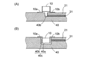
実施の形態1は、電位が異なる2つのバスバー間にフィルタ素子を接続する例であって、断面図で示す図1を参照しながら説明する。図1(A)にはリード線をバスバーの表面側(上側)に接続する例を示し、図1(B)にはリード線をバスバーと絶縁体との間に接続する例を示す。
[Embodiment 1]
The first embodiment is an example in which a filter element is connected between two bus bars having different potentials, and will be described with reference to FIG. 1 shown in a sectional view. FIG. 1A shows an example in which the lead wire is connected to the surface side (upper side) of the bus bar, and FIG. 1B shows an example in which the lead wire is connected between the bus bar and the insulator.
図1(A)および図1(B)に示すノイズフィルタ装置は、フィルタ素子10、バスバー20,21、絶縁体30,31、導電性筐体40などを有する。バスバー20とバスバー21との間は、端面が対向するように実装される。
The noise filter device shown in FIGS. 1A and 1B includes a
フィルタ素子10は、電位が異なるバスバー20とバスバー21との間を橋渡すように実装する。具体的には、フィルタ素子10のリード線10aをバスバー20に接続し、リード線10bをバスバー21に接続する。例えば溶接やハンダ等で行う接続は、図1(A)ではバスバー20,21の表面側(上側)に対して行い、図1(B)ではバスバー20,21の裏面側(下側;絶縁体30,31との間)に対して行う。このフィルタ素子10には、例えば金属キャップセラミックコンデンサ等を用いる。
The
導電性の板状部材としてのバスバー20,21は、例えば銅板を用いる。バスバー20は絶縁体30を介して導電性筐体40に実装され、バスバー21は絶縁体31を介して導電性筐体40に実装される。バスバー20と導電性筐体40との距離(言い換えれば絶縁体30の厚み)を「d」とし、絶縁体30の誘電率を「ε」とし、絶縁体30に接するバスバー20の面積を「S」とし、浮遊容量を「Cf」とする。このとき、式〔Cf=εS/d〕が成り立つ。実際の距離「d」は、例えば10〜300μm程度である。
For example, copper plates are used for the bus bars 20 and 21 as the conductive plate members. The
上記の式で明らかなように、断面積が大きくなったり、距離(厚み)が小さくなったりするにつれて浮遊容量が増す。このことは、バスバー21と導電性筐体40との間についても同様に成り立つ。こうして浮遊容量Cfが形成されるため、太破線で示すノイズの鎖交ループML1が生じる。絶縁体30,31の介在に伴って浮遊容量Cfが形成される点で、絶縁体30,31は「浮遊容量形成手段」に相当する。
As apparent from the above equation, the stray capacitance increases as the cross-sectional area increases or the distance (thickness) decreases. This also holds true between the
浮遊容量Cfの形成は、そこに同容量のコンデンサを接続したと同等の効果が得られるので、バスバー20,21自体がフィルタの役割を担う。また、バスバー20,21と導電性筐体40との距離を短く設定すると、バスバー20,21に流れる電流によって生じた熱が導電性筐体40に伝わり易くなる。したがって、バスバー20,21で発生した熱は導電性筐体40を通じて発散することができ、放熱性が向上する。なお、バスバー20,21と導電性筐体40との間の距離「d」を小さくするほど、浮遊容量Cfが増すとともに、バスバー20,21で生じた熱が導電性筐体40に伝わって放熱性が高まる。
Since the formation of the stray capacitance Cf has the same effect as a capacitor having the same capacitance connected thereto, the bus bars 20 and 21 themselves serve as filters. In addition, when the distance between the bus bars 20 and 21 and the
上述した実施の形態1によれば、以下に示す各効果を得ることができる。まず請求項1に対応し、バスバー20,21と導電性筐体40との間に絶縁体30,31(浮遊容量形成手段)を介在させて浮遊容量Cfを形成させ、電位が異なるバスバー20とバスバー21との間にフィルタ素子10を接続する構成とした(図1を参照)。この構成によれば、フィルタ素子10、バスバー20,21および導電性筐体40に鎖交ループML1が形成されてループ面積が縮小されるので、フィルタ素子10に対するノイズの鎖交を低減できる。また、絶縁体30,31によってバスバー20,21と導電性筐体40との間に距離「d」が生じて浮遊容量Cfが形成されるので、フィルタ効果を奏する。そのため、フィルタ素子10に対するノイズの鎖交をより確実に低減できる。
According to the first embodiment described above, the following effects can be obtained. Corresponding to claim 1, stray capacitance Cf is formed by interposing
請求項2に対応し、バスバー20,21と導電性筐体40との間に絶縁体30,31(浮遊容量形成手段)を介在させる絶縁体30,31(浮遊容量形成手段)を備える構成とした(図1を参照)。この構成によれば、簡単な構成でフィルタ素子10に対するノイズの鎖交を確実に低減することができる。
Corresponding to claim 2, a
〔実施の形態2〕
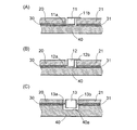
実施の形態2は、一方のバスバーが導電性筐体に接続された場合において、電位が異なる2つのバスバー間にフィルタ素子を接続する例であって、図2を参照しながら説明する。図2(A)には平面図を示し、図2(B)には図2(A)に図示する矢印方向からみた側面図を示し、図2(C)には回路図を示す。なお説明を簡単にするために、実施の形態1で用いた要素と同一の要素には同一の符号を付して説明を省略する。
[Embodiment 2]
Embodiment 2 is an example in which a filter element is connected between two bus bars having different potentials when one bus bar is connected to a conductive casing, and will be described with reference to FIG. 2A shows a plan view, FIG. 2B shows a side view seen from the direction of the arrow shown in FIG. 2A, and FIG. 2C shows a circuit diagram. In order to simplify the description, the same elements as those used in the first embodiment are denoted by the same reference numerals, and the description thereof is omitted.
図2(A)および図2(B)に示すノイズフィルタ装置は、フィルタ素子10〜12、バスバー20,21、絶縁体30,31、コイルL2、導電性筐体40などを有する。フィルタ素子10〜12は、いずれも電位が異なるバスバー20とバスバー21との間を橋渡すように並列的に実装する。ただし、フィルタ素子11,12は近接させて実装する。フィルタ素子10とフィルタ素子11との間には、バスバー21を囲むようにコイルL2を実装する。コイルL2には、例えばチョークコイル等のインダクタを用いる。
The noise filter device shown in FIGS. 2A and 2B includes
バスバー20,21は絶縁体30,31を介して導電性筐体40に実装する点は実施の形態1と同じであるので、浮遊容量Cfが生じる。このうちバスバー20については、さらに導電性締結部材B1,B2(例えば導電性ネジや導電性ボルト等)を用いて導電性筐体40に固定する。この固定によって、バスバー20は導電性筐体40と同電位になる。上述した要素にかかる回路図は、図2(C)に一点鎖線で囲む部分である。なお、フィルタ素子10の容量を「C1」とし、フィルタ素子11の容量を「C2」とし、フィルタ素子12の容量を「C3」とする。また、ダイオードD1,D2およびコイルL1は半波整流を行う整流回路を構成する。
Since the bus bars 20 and 21 are mounted on the
図2(C)に示す一点鎖線内には、太破線で示すノイズの鎖交ループML3,ML4が生じる。鎖交ループML3は、コイルL2、フィルタ素子11(C2)およびフィルタ素子12(C3)のループである。鎖交ループML4は、フィルタ素子11(C2)とフィルタ素子12(C3)のループである。その一方で一点鎖線外には、太破線で示すノイズの鎖交ループML2が生じる。この鎖交ループML2は、フィルタ素子10(C1)と整流回路との間に生じ、ダイオードD2、コイルL1およびフィルタ素子10(C1)のループである。 In the alternate long and short dash line shown in FIG. 2C, noise interlaced loops ML3 and ML4 indicated by thick broken lines are generated. Linkage loop ML3 is a loop of coil L2, filter element 11 (C2), and filter element 12 (C3). Linkage loop ML4 is a loop of filter element 11 (C2) and filter element 12 (C3). On the other hand, outside the alternate long and short dash line, an interlaced loop ML2 of noise indicated by a thick broken line is generated. This interlinkage loop ML2 is generated between the filter element 10 (C1) and the rectifier circuit, and is a loop of the diode D2, the coil L1, and the filter element 10 (C1).
上述した実施の形態2によれば、以下に示す各効果を得ることができる。まず請求項1に対応し、バスバー20,21と導電性筐体40との間に絶縁体30,31(浮遊容量形成手段)を介在させて浮遊容量を形成させ、電位が異なるバスバー20とバスバー21との間にフィルタ素子10〜12を並列接続する構成とした(図2を参照)。この構成によれば、フィルタ素子10〜12、バスバー20,21、コイルL2および導電性筐体40に鎖交ループML3,ML4が形成されてループ面積が縮小されるので(図2(C)を参照)、フィルタ素子10に対するノイズの鎖交を低減することができる。また、絶縁体30,31によってフィルタ効果を奏するので、フィルタ素子10〜12に対するノイズの鎖交をより確実に低減することができる。
According to the second embodiment described above, the following effects can be obtained. Corresponding to claim 1, a floating capacitance is formed by interposing
請求項2に対応し、バスバー20,21と導電性筐体40との間に絶縁体30,31(浮遊容量形成手段)を介在させる絶縁体30,31(浮遊容量形成手段)を備える構成とした(図2を参照)。この構成によれば、簡単な構成でフィルタ素子10に対するノイズの鎖交を確実に低減することができる。
Corresponding to claim 2, a
請求項3に対応し、複数のフィルタ素子10〜12のうちフィルタ素子11,12を近接させて実装し、電気的に並列接続する構成とした(図2(A)および図2(C)を参照)。この構成によれば、フィルタ素子11,12相互間のループ面積が縮小され、フィルタ素子11,12に対するノイズの鎖交を低減することができる。
Corresponding to claim 3, among the plurality of
請求項1に対応し、複数のバスバー20,21のうちで、バスバー20を導電性筐体40と電気的に接続して同電位にする構成とした(図2を参照)。この構成によれば、バスバー20と導電性筐体40とが接続によって同電位になるので、フィルタ素子10〜12と導電性筐体40との間のループ面積が縮小され、フィルタ素子10〜12に対するノイズの鎖交を低減することができる。
Corresponding to claim 1 , among the plurality of bus bars 20, 21, the
〔実施の形態3〕
実施の形態3は、一のバスバーを直接的に導電性筐体に実装する場合において、電位が異なる2つのバスバー間にフィルタ素子を接続する例であって、断面図で示す図3を参照しながら説明する。なお説明を簡単にするために、実施の形態1,2で用いた要素と同一の要素には同一の符号を付して説明を省略する。
[Embodiment 3]
The third embodiment is an example in which a filter element is connected between two bus bars having different potentials when one bus bar is directly mounted on a conductive housing. Refer to FIG. 3 shown in a sectional view. While explaining. In order to simplify the description, the same elements as those used in the first and second embodiments are denoted by the same reference numerals and the description thereof is omitted.
実施の形態3が実施の形態1と異なるのは、バスバー20を直接的に導電性筐体40に実装する点である。この実装は、溶接やハンダ等で行う。バスバー20と導電性筐体40とは同電位になって浮遊容量は生じないが、バスバー21と導電性筐体40との間には絶縁体31が介在するので浮遊容量が生じる。
The third embodiment is different from the first embodiment in that the
上述した実施の形態3によれば、バスバー21と導電性筐体40との間には浮遊容量が生じるので、この点において実施の形態1と同様の作用効果を得ることができる。この形態は、導電性筐体40が接地されている場合において、フィルタ素子10のリード線10a(一方側端子)を接地する場合に配線等が不要になってコストを低減できる。
According to the third embodiment described above, stray capacitance is generated between the
〔実施の形態4〕
実施の形態4は、導電性筐体に凹部を有する場合において、電位が異なる2つのバスバー間にフィルタ素子を接続する例であって、断面図で示す図4を参照しながら説明する。図4(A)には図1に対応する構成を示し、図4(B)には図3に対応する構成を示し、図4(C)には導電性筐体およびバスバーでノイズを遮蔽する構成を示す。なお説明を簡単にするために、実施の形態1〜3で用いた要素と同一の要素には同一の符号を付して説明を省略する。
[Embodiment 4]
The fourth embodiment is an example in which a filter element is connected between two bus bars having different potentials when a conductive casing has a concave portion, and will be described with reference to FIG. 4 shown in a sectional view. 4A shows a configuration corresponding to FIG. 1, FIG. 4B shows a configuration corresponding to FIG. 3, and FIG. 4C shields noise with a conductive housing and a bus bar. The configuration is shown. In order to simplify the description, the same elements as those used in the first to third embodiments are denoted by the same reference numerals, and the description thereof is omitted.
図4(A)に示すノイズフィルタ装置は、二点の相違を除いて、図1に示すノイズフィルタ装置と同等の形態である。第1に、導電性筐体40に凹部40aを備える点である。凹部40aの形状はフィルタ素子10が入れば任意であり、例えば窪形状や溝形状等が該当する。第2に、フィルタ素子10を上下逆方向に実装する点である。すなわち実施の形態1(図1)では導電性筐体40に対して「∩」字状で実装するのに対し、本形態では導電性筐体40に対して「U」字状で実装する。この実装によって、フィルタ素子10を凹部40a内に収容し、バスバー20,21の表面側(上側)はリード線10a,10bの厚みだけ突出するに過ぎない。
The noise filter device shown in FIG. 4A has the same form as the noise filter device shown in FIG. 1 except for two differences. First, the
図4(B)に示すノイズフィルタ装置は、二点の相違を除いて、図3に示すノイズフィルタ装置と同等の形態である。二点の相違は、上述した図4(A)に示すノイズフィルタ装置の場合と同じである。 The noise filter device shown in FIG. 4B has the same form as the noise filter device shown in FIG. 3 except for two differences. The difference between the two points is the same as in the case of the noise filter device shown in FIG.
図4(C)に示すノイズフィルタ装置は、二点の相違を除いて、上述した図4(B)に示すノイズフィルタ装置と同等の形態である。第1に、リード線10a,10bの接続位置が相違する。すなわち図4(B)に示すノイズフィルタ装置ではバスバー20,21の表面側(上側)に接続するのに対し、本形態ではリード線10aをバスバー20と導電性筐体40との間に挟み、リード線10bをバスバー21と絶縁体31との間に挟む。第2に、対向するバスバー20およびバスバー21の端面間は非接続状態を維持するために隙間を設けるが、当該隙間を可能な限りゼロに近づける。フィルタ素子10は、バスバー20,21と導電性筐体40(具体的には凹部40a)とに囲まれるのでノイズの影響を受けにくくなる。このようにノイズを遮蔽できる点で、バスバー20,21および導電性筐体40は「ノイズ遮蔽手段」に相当する。
The noise filter device shown in FIG. 4C has the same form as the noise filter device shown in FIG. 4B described above except for two differences. First, the connection positions of the
上述した実施の形態4によれば、以下に示す各効果を得ることができる。まず図4(A)の形態は実施の形態1と同等であるので、当該実施の形態1と同様の作用効果を得ることができる。図4(B)の形態は実施の形態3と同等であるので、当該実施の形態3と同様の作用効果を得ることができる。 According to the fourth embodiment described above, the following effects can be obtained. First, since the form of FIG. 4 (A) is equivalent to Embodiment 1, the same effect as Embodiment 1 can be obtained. Since the form of FIG. 4 (B) is equivalent to Embodiment 3, the same effect as Embodiment 3 can be obtained.
請求項4,6に対応し、フィルタ素子10の全部を覆ってノイズを遮蔽するバスバー20,21および導電性筐体40(ノイズ遮蔽手段)を備える構成とした(図4(C)を参照)。この構成によれば、バスバー20,21および導電性筐体40がフィルタ素子10の全部を覆うので、電磁誘導等によってフィルタ素子10が受けるノイズを低減することができる。また、別個のシールド部材を必要としないのでコストを低減できる。
Corresponding to claims 4 and 6, it is configured to include
〔実施の形態5〕
実施の形態5は、電位が異なる2つのバスバー間を接続するフィルタ素子をノイズ遮蔽手段で覆う例であって、断面図で示す図5を参照しながら説明する。図5(A)には図1に対応する構成を示し、図5(B)には図3に対応する構成を示し、図5(C)には図4(A)に対応する構成を示し、図5(D)には図4(B)に対応する構成を示す。なお説明を簡単にするために、実施の形態1〜4で用いた要素と同一の要素には同一の符号を付して説明を省略する。
[Embodiment 5]
Embodiment 5 is an example in which a filter element connecting two bus bars having different potentials is covered with a noise shielding means, and will be described with reference to FIG. 5 shown in a sectional view. 5A shows a configuration corresponding to FIG. 1, FIG. 5B shows a configuration corresponding to FIG. 3, and FIG. 5C shows a configuration corresponding to FIG. FIG. 5D shows a structure corresponding to FIG. In order to simplify the description, the same elements as those used in the first to fourth embodiments are denoted by the same reference numerals, and the description thereof is omitted.
図5(A)に示すノイズフィルタ装置は、図1に示すノイズフィルタ装置と比較して、フィルタ素子10およびバスバー20,21の全体を金属製カバー50で覆う点が相違する。この金属製カバー50は導電性締結部材B3,B4を用いて導電性筐体40に固定する。この固定によって、金属製カバー50は導電性筐体40と同電位になる。金属製カバー50は、ノイズを遮蔽可能な部材であれば形状や材質等は任意である。
The noise filter device shown in FIG. 5A differs from the noise filter device shown in FIG. 1 in that the
図5(B)〜図5(D)に示すノイズフィルタ装置は、各々が対応する図の形態と比較して、フィルタ素子10およびバスバー20,21の全体を金属製カバー50で覆う点が相違する。金属製カバー50は、図5(A)に示すノイズフィルタ装置と同様である。
The noise filter devices shown in FIGS. 5B to 5D are different from each other in that the
上述した実施の形態5によれば、以下に示す各効果を得ることができる。まず図5(A)の形態は実施の形態1と同等であるので、当該実施の形態1と同様の作用効果を得ることができる。図5(B)の形態は実施の形態3と同等であるので、当該実施の形態3と同様の作用効果を得ることができる。図5(C)および図5(D)の各形態は実施の形態4と同等であるので、当該実施の形態4と同様の作用効果を得ることができる。 According to the fifth embodiment described above, the following effects can be obtained. First, since the form of FIG. 5 (A) is equivalent to Embodiment 1, the same effect as Embodiment 1 can be obtained. Since the form of FIG. 5 (B) is equivalent to Embodiment 3, the same effect as Embodiment 3 can be obtained. Each form of FIG. 5C and FIG. 5D is equivalent to the fourth embodiment, and therefore, the same operational effects as those of the fourth embodiment can be obtained.
さらに請求項4,6に対応し、フィルタ素子10およびバスバー20,21の全部を覆ってノイズを遮蔽する金属製カバー50を備える構成とした(図5の各図を参照)。この構成によれば、金属製カバー50がフィルタ素子10の全部を覆うので、電磁誘導等によってフィルタ素子10が受けるノイズを低減することができる。また、バスバー20,21も覆うことができるのでノイズの遮蔽効果が向上する。
Further, according to claims 4 and 6, a configuration is provided in which a
〔実施の形態6〕
実施の形態6は、導電性筐体に凹部を有する場合において、電位が異なる2つのバスバー間にフィルタ素子を接続する例であって、断面図で示す図6を参照しながら説明する。なお説明を簡単にするために、実施の形態1〜5で用いた要素と同一の要素には同一の符号を付して説明を省略する。
[Embodiment 6]
Embodiment 6 is an example in which a filter element is connected between two bus bars having different potentials when a conductive casing has a recess, and will be described with reference to FIG. 6 shown in a sectional view. In order to simplify the description, the same elements as those used in the first to fifth embodiments are denoted by the same reference numerals, and the description thereof is omitted.
図6(A)に示すノイズフィルタ装置は、図4(A)に示すノイズフィルタ装置と比較して、バスバー20,21と導電性筐体40との間だけでなく、フィルタ素子10と導電性筐体40との間にも絶縁体32を介在させる点が相違する。この絶縁体32は、絶縁体30と絶縁体31とを一体化させるとともに、凹部40aに対応する部位をも一体化させる。この構成では、実施の形態1で説明したようにバスバー20,21と導電性筐体40との間に浮遊容量が生じるだけでなく、フィルタ素子10と導電性筐体40との間にも浮遊容量が生じる。実際に生じる浮遊容量の大きさは、式〔Cf=εS/d〕に従うため、導電性筐体40に対応する部材との間で相違する。
Compared with the noise filter device shown in FIG. 4 (A), the noise filter device shown in FIG. 6 (A) is not only between the bus bars 20 and 21 and the
上述した実施の形態6によれば、図4(A)に示す形態と同等であるので、当該実施の形態1,4と同様の作用効果を得ることができる。さらに、フィルタ素子10と導電性筐体40との間にも浮遊容量が生じるので、ループ面積がさらに縮小され、フィルタ素子10に対するノイズの鎖交をより低減できる。
According to the above-described sixth embodiment, since it is equivalent to the embodiment shown in FIG. 4A, the same effects as those of the first and fourth embodiments can be obtained. Furthermore, since stray capacitance is also generated between the
〔実施の形態7〕
実施の形態7は、電位が異なるバスバーと導電性筐体との間にフィルタ素子を接続する例であって、断面図で示す図7を参照しながら説明する。図7(A)には段差部を備える導電性筐体への実装例を示し、図7(B)には複合凹部を備える導電性筐体への実装例を示す。なお説明を簡単にするために、実施の形態1〜6で用いた要素と同一の要素には同一の符号を付して説明を省略する。
[Embodiment 7]
The seventh embodiment is an example in which a filter element is connected between a bus bar having a different potential and a conductive casing, and will be described with reference to FIG. 7 shown in a sectional view. FIG. 7A shows an example of mounting on a conductive casing provided with a stepped portion, and FIG. 7B shows an example of mounting on a conductive casing provided with a composite recess. In order to simplify the description, the same elements as those used in the first to sixth embodiments are denoted by the same reference numerals, and the description thereof is omitted.
図7(A)に示すノイズフィルタ装置は、導電性筐体40が段差部40bを備える点を除いて、図3に示すノイズフィルタ装置と同等の形態である。言い換えれば、バスバー20に対応する部位を導電性筐体40で形成する。よって、フィルタ素子10のリード線10aは導電性筐体40に直接的に接続される。
The noise filter device shown in FIG. 7A has the same form as the noise filter device shown in FIG. 3 except that the
図7(B)に示すノイズフィルタ装置は、導電性筐体40が複合凹部40cを備える点を除いて、図4(B)に示すノイズフィルタ装置と同等の形態である。複合凹部40cは、段差部40bと凹部40aとを組み合わせた部位である。バスバー20に対応する部位を導電性筐体40で形成する点と、フィルタ素子10のリード線10aを導電性筐体40に直接的に接続する点は、上述した図7(A)と同等の形態である。
The noise filter device shown in FIG. 7 (B) has the same form as the noise filter device shown in FIG. 4 (B) except that the
上述した実施の形態7によれば、図7(A)の形態は実施の形態3と同等であるので、当該実施の形態3と同様の作用効果を得ることができる。また図7(B)の形態は実施の形態4と同等であるので、当該実施の形態4と同様の作用効果を得ることができる。 According to the seventh embodiment described above, the form of FIG. 7A is equivalent to the third embodiment, and therefore the same operational effects as those of the third embodiment can be obtained. 7B is the same as that of the fourth embodiment, and the same effect as that of the fourth embodiment can be obtained.
〔実施の形態8〕
実施の形態8は、電位が異なる2つのバスバー間にフィルタ素子を接続する例であって、断面図で示す図8を参照しながら説明する。図8(A)には複数の凹部を備える導電性筐体に実装する例を示し、図8(B)には凸部を備える導電性筐体に実装する例を示し、図8(C)には一の凹部を備える導電性筐体に実装する例を示し、図8(D)には一の段差部を備える導電性筐体に実装する例を示す。なお説明を簡単にするために、実施の形態1〜7で用いた要素と同一の要素には同一の符号を付して説明を省略する。
[Embodiment 8]
Embodiment 8 is an example in which a filter element is connected between two bus bars having different potentials, and will be described with reference to FIG. 8 shown in a sectional view. FIG. 8A shows an example of mounting on a conductive casing having a plurality of concave portions, FIG. 8B shows an example of mounting on a conductive casing having convex portions, and FIG. FIG. 8D shows an example of mounting on a conductive casing provided with one recess, and FIG. 8D shows an example of mounting on a conductive casing provided with one stepped portion. In order to simplify the description, the same elements as those used in the first to seventh embodiments are denoted by the same reference numerals, and the description thereof is omitted.
図8(A)および図8(B)に示すノイズフィルタ装置は、図1(A)に示すノイズフィルタ装置に対応するが、二点の相違がある。第1に、バスバー20,21および導電性筐体40の表面(上面)がフラットになるように、図8(A)では2つの凹部40aを備え、図8(B)では1つの凸部40dを備える点である。第2に、絶縁体33〜36の断面形状を導電性筐体40の断面形状に合わせるため、図8(A)では上方に開口する「コ」字状に形成し、図8(B)では「L」字状に形成する点である。
The noise filter device shown in FIGS. 8A and 8B corresponds to the noise filter device shown in FIG. 1A, but there are two differences. First, two
図8(A)の形態における実装手順は、導電性筐体40に形成された2つの凹部40aにそれぞれ絶縁体33,34を実装(装着)し、その上側にバスバー20,21を実装(嵌め込み)し、フィルタ素子10はバスバー20,21相互間を橋渡すように接続する。図8(B)の形態における実装手順は、導電性筐体40に形成された1つの凸部40dを除く部位にそれぞれ絶縁体35,36を実装(装着)し、その上側にバスバー20,21を実装し、フィルタ素子10はバスバー20,21相互間を橋渡すように接続する。
In the mounting procedure in the form of FIG. 8A, the
図8(C)および図8(D)に示すノイズフィルタ装置は、図7(A)に示すノイズフィルタ装置に対応するが、二点の相違がある。この相違は、上述した図8(A)および図8(B)に示すノイズフィルタ装置と図1(A)に示すノイズフィルタ装置との相違と同じである。図8(C)および図8(D)の形態における各実装手順は、絶縁体34およびバスバー21を実装し、フィルタ素子10は導電性筐体40とバスバー21との相互間を橋渡すように接続する点を除いて、図8(A)および図8(B)の形態における各実装手順と同じである。
The noise filter device shown in FIGS. 8C and 8D corresponds to the noise filter device shown in FIG. 7A, but there are two differences. This difference is the same as the difference between the noise filter device shown in FIGS. 8A and 8B and the noise filter device shown in FIG. 8C and 8D, the mounting procedure is such that the
上述した実施の形態8によれば、図8(A)および図8(B)の形態は実施の形態1と同等であるので、当該実施の形態1と同様の作用効果を得ることができる。図8(C)および図8(D)の形態は実施の形態7と同等であるので、当該実施の形態7と同様の作用効果を得ることができる。さらに、バスバー20,21および導電性筐体40の表面(上面)がフラットになるので、フィルタ素子10等の回路素子が実装し易くなる。
According to the above-described eighth embodiment, the forms of FIG. 8A and FIG. 8B are equivalent to the first embodiment, and therefore the same operational effects as those of the first embodiment can be obtained. 8 (C) and FIG. 8 (D) are equivalent to the seventh embodiment, and therefore, the same effects as those of the seventh embodiment can be obtained. Furthermore, since the surfaces (upper surfaces) of the bus bars 20 and 21 and the
〔実施の形態9〕
実施の形態9は、電位が異なる2つのバスバー間にフィルタ素子を接続する例であって、断面図で示す図9を参照しながら説明する。図9は2つのバスバー相互間(隙間)にフィルタ素子を実装する例であって、図9(A),図9(B),図9(C)にはそれぞれ異なる形態のリード線を有するフィルタ素子を示す。各図に共通する事項として、バスバー20とバスバー21との間は端面を対向させ、かつフィルタ素子11〜13を実装可能な空間を確保する。なお説明を簡単にするために、実施の形態1〜8で用いた要素と同一の要素には同一の符号を付して説明を省略する。
[Embodiment 9]
Embodiment 9 is an example in which a filter element is connected between two bus bars having different potentials, and will be described with reference to FIG. 9 shown in a sectional view. FIG. 9 shows an example in which a filter element is mounted between two bus bars (gap). FIGS. 9A, 9B, and 9C show filters having different forms of lead wires. An element is shown. As matters common to the drawings, the end surfaces of the
図9(A)に示すノイズフィルタ装置は、フィルタ素子11、バスバー20,21、絶縁体30,31、導電性筐体40などを有する。フィルタ素子11は、側面から見て直線状(平板状または棒状)のリード線11a,11bを備える。一方のリード線(本例ではリード線11a)を一方のバスバー(本例ではバスバー20)と絶縁体(本例では絶縁体30)との間に挟んで、一方のバスバーに接続する。他方のリード線(本例ではリード線11b)を他方のバスバー(本例ではバスバー21)の表面側(上側)に接続する。
The noise filter device illustrated in FIG. 9A includes a
図9(B)に示すノイズフィルタ装置は、フィルタ素子12、バスバー20,21、絶縁体30,31、導電性筐体40などを有する。フィルタ素子12は、側面から見て「L」字状のリード線12a,12bを備える。フィルタ素子12の接続形態は、図9(A)に示すフィルタ素子11の接続形態と同じである。
The noise filter device illustrated in FIG. 9B includes a
図9(C)に示すノイズフィルタ装置は、フィルタ素子13、バスバー20,21、絶縁体30,31、導電性筐体40などを有する。フィルタ素子13は、側面から見て「T」字状のリード線13a,13bを備える。リード線13aは、バスバー20と絶縁体30との間に挟んで、バスバー20に接続する。リード線13bは、バスバー21と絶縁体31との間に挟んで、バスバー21に接続する。導電性筐体40には、フィルタ素子13の一部を収容するための凹部40aを備える。
The noise filter device illustrated in FIG. 9C includes a
上述した実施の形態9によれば、図9(A)と図9(B)に示す各形態は、実施の形態1における図1(A)の一方と図1(B)の一方とをそれぞれ組み合わせた形態に等しい。また、図9(C)に示す形態は、実施の形態1における図1(B)の形態に等しい。したがって、実施の形態1と同様の作用効果を得ることができる。 According to Embodiment 9 described above, each of the forms shown in FIGS. 9A and 9B is different from the one in FIG. 1A and the one in FIG. Equal to the combined form. The form shown in FIG. 9C is equivalent to the form shown in FIG. Therefore, the same effect as that of the first embodiment can be obtained.
〔実施の形態10〕
実施の形態10は、電位が異なる2つのバスバー間を接続するフィルタ素子をノイズ遮蔽手段で覆う例であって、断面図で示す図10を参照しながら説明する。なお説明を簡単にするために、実施の形態1〜9で用いた要素と同一の要素には同一の符号を付して説明を省略する。
[Embodiment 10]
The tenth embodiment is an example in which a filter element that connects two bus bars having different potentials is covered with a noise shielding means, and will be described with reference to FIG. 10 shown in a sectional view. In order to simplify the description, the same elements as those used in the first to ninth embodiments are denoted by the same reference numerals, and the description thereof is omitted.
図10に示すノイズフィルタ装置は、図5(C)に示すノイズフィルタ装置と比較して、フィルタ素子10およびバスバー20の全体を金属製カバー51で覆う点が相違する。この金属製カバー51は、導電性締結部材B5を用いて導電性筐体40に固定し、導電性締結部材B6を用いてバスバー21に固定する。この固定によって、金属製カバー51およびバスバー21は導電性筐体40と同電位になる。金属製カバー51は「ノイズ遮蔽手段」に相当し、上述した金属製カバー50とは形状が異なる点を除いて同じである。
The noise filter device shown in FIG. 10 is different from the noise filter device shown in FIG. 5C in that the
上述した実施の形態10によれば、図10の形態は実施の形態5と同等であるので、当該実施の形態5と同様の作用効果を得ることができる。 According to the tenth embodiment described above, the form of FIG. 10 is equivalent to the fifth embodiment, and thus the same operational effects as those of the fifth embodiment can be obtained.
〔実施の形態11〕
実施の形態11は、電位が異なる3つのバスバー間を接続するフィルタ素子を実装する例であって、図11を参照しながら説明する。図11(A)には平面図を示し、図11(B)には図11(A)に図示するXIB−XIB線矢視の断面図を示す。なお説明を簡単にするために、実施の形態1〜10で用いた要素と同一の要素には同一の符号を付して説明を省略する。
[Embodiment 11]
The eleventh embodiment is an example of mounting a filter element that connects three bus bars having different potentials, and will be described with reference to FIG. 11A is a plan view, and FIG. 11B is a cross-sectional view taken along line XIB-XIB shown in FIG. 11A. In order to simplify the description, the same elements as those used in Embodiments 1 to 10 are denoted by the same reference numerals, and the description thereof is omitted.
図11(A)に示すノイズフィルタ装置は、フィルタ素子14、バスバー20,21,22、絶縁体30,31,33、導電性筐体40などを有する。フィルタ素子14はいわゆる「3端子フィルタ」と呼ばれ、リード線14a,14c,14dを備える。このフィルタ素子14には、例えば株式会社村田製作所製の「NFM21PCシリーズ」などを適用できる。リード線14aはバスバー20に接続し、リード線14cはバスバー21に接続し、リード線14d(あるいはリード線14b)はバスバー22に接続する。
The noise filter device shown in FIG. 11A includes a
バスバー20とバスバー21との間は端面が対向するように左右方向に実装され、相互間を通るようにバスバー22が上下方向に実装される。バスバー22は導電性締結部材B7,B8を用いて導電性筐体40に固定する。この固定によってバスバー22は導電性筐体40と同電位になり、特に導電性筐体40が接地されている場合は0[V]になる。
The
上述した実施の形態11によれば、実施の形態1〜10に示すフィルタ素子10〜13(2端子フィルタ)に代えて、フィルタ素子14を用いるに過ぎない。したがって、実施の形態1〜10と同様の作用効果を得ることができる。
According to the eleventh embodiment described above, only the
〔実施の形態12〕
実施の形態12は、電位が異なる4つのバスバー間を並列的に接続するフィルタ素子を実装する例であって、図12を参照しながら説明する。図12(A)には平面図を示し、図12(B)には図12(A)に図示するXIIB−XIIB線矢視の断面図を示す。なお説明を簡単にするために、実施の形態1〜10で用いた要素と同一の要素には同一の符号を付して説明を省略する。
[Embodiment 12]
The twelfth embodiment is an example of mounting a filter element that connects four bus bars having different potentials in parallel, and will be described with reference to FIG. 12A shows a plan view, and FIG. 12B shows a cross-sectional view taken along the line XIIB-XIIB shown in FIG. 12A. In order to simplify the description, the same elements as those used in Embodiments 1 to 10 are denoted by the same reference numerals, and the description thereof is omitted.
図12(A)に示すノイズフィルタ装置は、フィルタ素子15、バスバー21〜28、絶縁体30、導電性筐体40などを有する。フィルタ素子15はいわゆる「フィルタアレイ」と呼ばれ、複数(本例は8)本のリード線15a〜15hを備える。このフィルタ素子15には、例えばTDK株式会社製の「CKCシリーズ」などを適用できる。フィルタ素子15の中には、図示するように4つのコンデンサが並列的に回路形成されている。上側のリード線15aはバスバー21に接続し、リード線15bはバスバー22に接続し、リード線15cはバスバー23に接続し、リード線15dはバスバー24に接続する。下側のリード線15eはバスバー25に接続し、リード線15fはバスバー26に接続し、リード線15gはバスバー27に接続し、リード線15hはバスバー28に接続する。
The noise filter device illustrated in FIG. 12A includes a
バスバー21とバスバー25との間は端面が対向するように上下方向に実装される。同様にして、バスバー22とバスバー26との間、バスバー23とバスバー27との間、バスバー24とバスバー28との間についても端面が対向するように上下方向に実装される。接続を行うバスバー間の電位が異なっていればよい。例えば、バスバー21は24[V]、バスバー22,24,25は12[V]、バスバー23,28は5[V]、バスバー26,27は0[V](GNDすなわち接地)である。バスバー21〜28と導電性筐体40との間には、絶縁体30が介在して実装される。
The
上述した実施の形態12によれば、実施の形態1〜10に示すフィルタ素子10〜13(2端子フィルタ)に代えて、フィルタ素子15を用いるに過ぎない。したがって、実施の形態1〜10と同様の作用効果を得ることができる。
According to the above-described twelfth embodiment, only the
〔他の実施の形態〕
以上では本発明を実施するための形態について実施の形態1〜12に従って説明したが、本発明は当該形態に何ら限定されるものではない。言い換えれば、本発明の要旨を逸脱しない範囲内において、種々なる形態で実施することもできる。例えば、次に示す各形態を実現してもよい。
[Other Embodiments]
In the above, although the form for implementing this invention was demonstrated according to Embodiment 1-12, this invention is not limited to the said form at all. In other words, various forms can be implemented without departing from the scope of the present invention. For example, the following forms may be realized.
上述した実施の形態1〜12では、導電性の板状部材としてのバスバー20〜28は銅板を用いる構成とした。この形態に代えて、銅板以外の導電性の板状部材を用いてもよい。例えば、金属部材(例えばアルミニウム,亜鉛,マグネシウム、あるいはそれらの合金)や、導電性高分子などが該当する。これらの部材を用いた場合でも、浮遊容量を生じさせることができるので、実施の形態1〜12と同様の作用効果を得ることができる。 In Embodiment 1-12 mentioned above, the bus-bars 20-28 as an electroconductive plate-shaped member were set as the structure which uses a copper plate. Instead of this form, a conductive plate member other than a copper plate may be used. For example, a metal member (for example, aluminum, zinc, magnesium, or an alloy thereof) or a conductive polymer is applicable. Even when these members are used, stray capacitance can be generated, so that the same effects as those of the first to twelfth embodiments can be obtained.
上述した実施の形態1〜12では、バスバー20〜28を導電性筐体40に実装する構成とした(図1〜図12を参照)。この形態に代えて、バスバー20〜28を他の実装対象物に実装する構成としてもよい。他の実装対象物には、例えば電気回路を構成する基板(多層基板を含む)などが該当する。他の実装対象を用いた場合でも、物浮遊容量を生じさせることができるので、実施の形態1〜12と同様の作用効果を得ることができる。 In Embodiment 1-12 mentioned above, it was set as the structure which mounts the bus-bars 20-28 in the electroconductive housing | casing 40 (refer FIGS. 1-12). Instead of this form, the bus bars 20 to 28 may be mounted on other mounting objects. For example, a substrate (including a multilayer substrate) constituting an electric circuit corresponds to the other mounting target. Even when other mounting targets are used, the stray capacitance can be generated, so that the same effects as those of the first to twelfth embodiments can be obtained.
上述した実施の形態1〜12では、浮遊容量形成手段として絶縁体30〜36を適用した(図1〜図12を参照)。この形態に代えて、バスバー(導電性の板状部材)と導電性筐体とについて、対向面に隙間を形成する隙間形成手段を適用してもよい。隙間形成手段は、バスバーおよび導電性筐体のうち一方または双方に設ける突起や、バスバーと導電性筐体との間に介在させる小片の絶縁体などが該当する。対向面に形成される隙間には浮遊容量が生じるので、実施の形態1〜12と同様の作用効果を得ることができる。
In the first to twelfth embodiments described above, the
上述した実施の形態5,10では、フィルタ素子10およびバスバー20,21の全部を覆う金属製カバー50,51を備える構成とした(図5,図10を参照)。この形態に代えて、フィルタ素子10およびバスバー20,21の一部を覆う金属製カバーを備える構成としてもよい。ノイズ遮蔽手段としての金属製カバーで覆われた部位については、ノイズを遮蔽することができるので、全く覆われない場合に比べてノイズを遮蔽することができる。したがって、電流や信号等に及ぼす影響を抑えることができる。
In
10〜15 フィルタ素子
20〜28 バスバー(導電性の板状部材)
30〜36 絶縁体(浮遊容量形成手段)
40 導電性筐体(実装対象物)
50,51 金属製カバー(ノイズ遮蔽手段)
C1〜C3 コンデンサ
D1,D2 ダイオード
L1,L2 インダクタ
10-15 Filter element 20-28 Bus bar (conductive plate-like member)
30-36 insulator (floating capacitance forming means)
40 Conductive housing (object to be mounted)
50, 51 Metal cover (noise shielding means)
C1-C3 Capacitor D1, D2 Diode L1, L2 Inductor
Claims (6)
前記バスバーと前記導電性筐体との間に浮遊容量を形成する浮遊容量形成手段と、
電位が異なる前記バスバーの相互間と、接地される前記導電性筐体と前記バスバーとの間と、のうち一以上の部材間を電気的に接続するフィルタ素子とを有し、
複数の前記バスバーを前記導電性筐体に実装する場合には、前記導電性筐体と電気的に接続する場合を含めて複数の前記バスバーのうち一以上の前記バスバーを接地して同電位にすることを特徴とするノイズフィルタ装置。 In a noise filter device mounted on a conductive housing together with a bus bar which is a conductive plate member,
Stray capacitance forming means for forming stray capacitance between the bus bar and the conductive casing;
A filter element that electrically connects one or more members among the bus bars having different potentials, and between the conductive housing and the bus bar that are grounded;
When implementing a plurality of the bus bar to the conductive housing is at the same potential by grounding one or more of the bus bar of the plurality of the bus bars including a case of connecting to the conductive housing and electrical A noise filter device characterized by:
Priority Applications (1)
| Application Number | Priority Date | Filing Date | Title |
|---|---|---|---|
| JP2010090515A JP5594517B2 (en) | 2010-04-09 | 2010-04-09 | Noise filter device |
Applications Claiming Priority (1)
| Application Number | Priority Date | Filing Date | Title |
|---|---|---|---|
| JP2010090515A JP5594517B2 (en) | 2010-04-09 | 2010-04-09 | Noise filter device |
Publications (2)
| Publication Number | Publication Date |
|---|---|
| JP2011223314A JP2011223314A (en) | 2011-11-04 |
| JP5594517B2 true JP5594517B2 (en) | 2014-09-24 |
Family
ID=45039703
Family Applications (1)
| Application Number | Title | Priority Date | Filing Date |
|---|---|---|---|
| JP2010090515A Active JP5594517B2 (en) | 2010-04-09 | 2010-04-09 | Noise filter device |
Country Status (1)
| Country | Link |
|---|---|
| JP (1) | JP5594517B2 (en) |
Families Citing this family (4)
| Publication number | Priority date | Publication date | Assignee | Title |
|---|---|---|---|---|
| JP5707435B2 (en) | 2013-02-21 | 2015-04-30 | 株式会社日本自動車部品総合研究所 | Noise filter |
| JP6065671B2 (en) | 2013-03-15 | 2017-01-25 | オムロン株式会社 | Measuring device and mounting unit |
| EP3048726A4 (en) * | 2013-09-17 | 2017-07-12 | Mitsubishi Electric Corporation | Noise filter |
| JP7135999B2 (en) * | 2019-05-13 | 2022-09-13 | 株式会社オートネットワーク技術研究所 | wiring board |
Family Cites Families (2)
| Publication number | Priority date | Publication date | Assignee | Title |
|---|---|---|---|---|
| JPH05161268A (en) * | 1991-12-02 | 1993-06-25 | Yokogawa Electric Corp | Mounting structure for noise filter |
| JP4743536B2 (en) * | 2006-10-16 | 2011-08-10 | 株式会社デンソー | Semiconductor mounting structure |
-
2010
- 2010-04-09 JP JP2010090515A patent/JP5594517B2/en active Active
Also Published As
| Publication number | Publication date |
|---|---|
| JP2011223314A (en) | 2011-11-04 |
Similar Documents
| Publication | Publication Date | Title |
|---|---|---|
| EP2800218B1 (en) | Busbar device with noise filter | |
| US9345160B2 (en) | Electronic device | |
| JP6193405B2 (en) | Filter device | |
| JP5327289B2 (en) | Power converter | |
| US10979014B2 (en) | Voltage filter and power conversion device | |
| JP5594517B2 (en) | Noise filter device | |
| JP7213407B2 (en) | capacitor | |
| KR101695492B1 (en) | Device for reducing the interference emission in a power electronic system | |
| JP2017130444A (en) | Cable connector | |
| CN107148731B (en) | Power conversion device | |
| JP5286150B2 (en) | Semiconductor device for power conversion | |
| JPWO2018051656A1 (en) | Capacitor | |
| CN105551799A (en) | Electronic component | |
| JP4861558B2 (en) | Filter device for at least one electrical wiring connected to the case from the outside | |
| JP6305731B2 (en) | Case mold type capacitor and manufacturing method thereof | |
| JP6547610B2 (en) | Power converter | |
| JP6696071B2 (en) | Output noise reduction device | |
| CN112187970B (en) | Camera module and electronic device thereof | |
| CN110858513B (en) | Inductor(s) | |
| CN110797314A (en) | Assembly | |
| JP5320801B2 (en) | Electronic device and noise shielding method thereof | |
| JP2004014862A (en) | Wiring structure | |
| WO2021075171A1 (en) | Power supply module and mass spectrometry device | |
| JP7461531B2 (en) | Composite Capacitor | |
| CN109661708B (en) | Choke coil |
Legal Events
| Date | Code | Title | Description |
|---|---|---|---|
| A621 | Written request for application examination |
Free format text: JAPANESE INTERMEDIATE CODE: A621 Effective date: 20120611 |
|
| A977 | Report on retrieval |
Free format text: JAPANESE INTERMEDIATE CODE: A971007 Effective date: 20130306 |
|
| A131 | Notification of reasons for refusal |
Free format text: JAPANESE INTERMEDIATE CODE: A131 Effective date: 20130523 |
|
| A521 | Request for written amendment filed |
Free format text: JAPANESE INTERMEDIATE CODE: A523 Effective date: 20130701 |
|
| A131 | Notification of reasons for refusal |
Free format text: JAPANESE INTERMEDIATE CODE: A131 Effective date: 20140403 |
|
| A521 | Request for written amendment filed |
Free format text: JAPANESE INTERMEDIATE CODE: A523 Effective date: 20140508 |
|
| TRDD | Decision of grant or rejection written | ||
| A01 | Written decision to grant a patent or to grant a registration (utility model) |
Free format text: JAPANESE INTERMEDIATE CODE: A01 Effective date: 20140710 |
|
| A61 | First payment of annual fees (during grant procedure) |
Free format text: JAPANESE INTERMEDIATE CODE: A61 Effective date: 20140723 |
|
| R151 | Written notification of patent or utility model registration |
Ref document number: 5594517 Country of ref document: JP Free format text: JAPANESE INTERMEDIATE CODE: R151 |
|
| R250 | Receipt of annual fees |
Free format text: JAPANESE INTERMEDIATE CODE: R250 |
|
| R250 | Receipt of annual fees |
Free format text: JAPANESE INTERMEDIATE CODE: R250 |
|
| R250 | Receipt of annual fees |
Free format text: JAPANESE INTERMEDIATE CODE: R250 |
|
| R250 | Receipt of annual fees |
Free format text: JAPANESE INTERMEDIATE CODE: R250 |
|
| R250 | Receipt of annual fees |
Free format text: JAPANESE INTERMEDIATE CODE: R250 |
|
| R250 | Receipt of annual fees |
Free format text: JAPANESE INTERMEDIATE CODE: R250 |
|
| R250 | Receipt of annual fees |
Free format text: JAPANESE INTERMEDIATE CODE: R250 |