JP5591480B2 - Method and system for minimizing vibration rectification errors in a magnetic circuit accelerometer - Google Patents
Method and system for minimizing vibration rectification errors in a magnetic circuit accelerometer Download PDFInfo
- Publication number
- JP5591480B2 JP5591480B2 JP2009063045A JP2009063045A JP5591480B2 JP 5591480 B2 JP5591480 B2 JP 5591480B2 JP 2009063045 A JP2009063045 A JP 2009063045A JP 2009063045 A JP2009063045 A JP 2009063045A JP 5591480 B2 JP5591480 B2 JP 5591480B2
- Authority
- JP
- Japan
- Prior art keywords
- piece
- ring
- accelerometer
- pole piece
- magnet
- Prior art date
- Legal status (The legal status is an assumption and is not a legal conclusion. Google has not performed a legal analysis and makes no representation as to the accuracy of the status listed.)
- Expired - Fee Related
Links
Images

Classifications
-
- G—PHYSICS
- G01—MEASURING; TESTING
- G01P—MEASURING LINEAR OR ANGULAR SPEED, ACCELERATION, DECELERATION, OR SHOCK; INDICATING PRESENCE, ABSENCE, OR DIRECTION, OF MOVEMENT
- G01P15/00—Measuring acceleration; Measuring deceleration; Measuring shock, i.e. sudden change of acceleration
- G01P15/02—Measuring acceleration; Measuring deceleration; Measuring shock, i.e. sudden change of acceleration by making use of inertia forces using solid seismic masses
- G01P15/08—Measuring acceleration; Measuring deceleration; Measuring shock, i.e. sudden change of acceleration by making use of inertia forces using solid seismic masses with conversion into electric or magnetic values
- G01P15/13—Measuring acceleration; Measuring deceleration; Measuring shock, i.e. sudden change of acceleration by making use of inertia forces using solid seismic masses with conversion into electric or magnetic values by measuring the force required to restore a proofmass subjected to inertial forces to a null position
- G01P15/132—Measuring acceleration; Measuring deceleration; Measuring shock, i.e. sudden change of acceleration by making use of inertia forces using solid seismic masses with conversion into electric or magnetic values by measuring the force required to restore a proofmass subjected to inertial forces to a null position with electromagnetic counterbalancing means
-
- G—PHYSICS
- G01—MEASURING; TESTING
- G01P—MEASURING LINEAR OR ANGULAR SPEED, ACCELERATION, DECELERATION, OR SHOCK; INDICATING PRESENCE, ABSENCE, OR DIRECTION, OF MOVEMENT
- G01P15/00—Measuring acceleration; Measuring deceleration; Measuring shock, i.e. sudden change of acceleration
- G01P15/02—Measuring acceleration; Measuring deceleration; Measuring shock, i.e. sudden change of acceleration by making use of inertia forces using solid seismic masses
- G01P15/08—Measuring acceleration; Measuring deceleration; Measuring shock, i.e. sudden change of acceleration by making use of inertia forces using solid seismic masses with conversion into electric or magnetic values
- G01P15/11—Measuring acceleration; Measuring deceleration; Measuring shock, i.e. sudden change of acceleration by making use of inertia forces using solid seismic masses with conversion into electric or magnetic values by inductive pick-up
-
- G—PHYSICS
- G01—MEASURING; TESTING
- G01P—MEASURING LINEAR OR ANGULAR SPEED, ACCELERATION, DECELERATION, OR SHOCK; INDICATING PRESENCE, ABSENCE, OR DIRECTION, OF MOVEMENT
- G01P15/00—Measuring acceleration; Measuring deceleration; Measuring shock, i.e. sudden change of acceleration
- G01P15/02—Measuring acceleration; Measuring deceleration; Measuring shock, i.e. sudden change of acceleration by making use of inertia forces using solid seismic masses
- G01P15/08—Measuring acceleration; Measuring deceleration; Measuring shock, i.e. sudden change of acceleration by making use of inertia forces using solid seismic masses with conversion into electric or magnetic values
- G01P2015/0805—Measuring acceleration; Measuring deceleration; Measuring shock, i.e. sudden change of acceleration by making use of inertia forces using solid seismic masses with conversion into electric or magnetic values being provided with a particular type of spring-mass-system for defining the displacement of a seismic mass due to an external acceleration
- G01P2015/0822—Measuring acceleration; Measuring deceleration; Measuring shock, i.e. sudden change of acceleration by making use of inertia forces using solid seismic masses with conversion into electric or magnetic values being provided with a particular type of spring-mass-system for defining the displacement of a seismic mass due to an external acceleration for defining out-of-plane movement of the mass
- G01P2015/0825—Measuring acceleration; Measuring deceleration; Measuring shock, i.e. sudden change of acceleration by making use of inertia forces using solid seismic masses with conversion into electric or magnetic values being provided with a particular type of spring-mass-system for defining the displacement of a seismic mass due to an external acceleration for defining out-of-plane movement of the mass for one single degree of freedom of movement of the mass
- G01P2015/0828—Measuring acceleration; Measuring deceleration; Measuring shock, i.e. sudden change of acceleration by making use of inertia forces using solid seismic masses with conversion into electric or magnetic values being provided with a particular type of spring-mass-system for defining the displacement of a seismic mass due to an external acceleration for defining out-of-plane movement of the mass for one single degree of freedom of movement of the mass the mass being of the paddle type being suspended at one of its longitudinal ends
Landscapes
- Physics & Mathematics (AREA)
- General Physics & Mathematics (AREA)
- Electromagnetism (AREA)
- Finish Polishing, Edge Sharpening, And Grinding By Specific Grinding Devices (AREA)
- Transmission And Conversion Of Sensor Element Output (AREA)
- Measuring Fluid Pressure (AREA)
Description
図1に示す加速度計のような従来の加速度計の磁気帰還路は、可撓性のプルーフ・マス(proof mass;試験質量)に取り付けられたコイルと相互作用する励磁リングと磁極片の間の空隙に磁束分布を作り出す。磁束は、コイル中の電流と相互作用して、素子(device)が受ける加速度に比例した再バランス力を生み出す。空隙を横切る磁束密度は、実用的な回路を構成する幾何学的な制約により、一様ではない。更に、磁気回路の磁界強度は、電流方向の変化を伴って磁界がコイルと相互作用すると、一定ではない。磁界強度は磁石の微小ループ勾配に追随する。素子が、磁束及び磁束自体の大きさに関してコイルの方向性(orientation)を変化させ得る振動を受けると、素子の出力は測定される加速度とは無関係に変化するであろう。このエラーは振動整流エラー(vibration rectification error:VRE)と称されている。 The magnetic feedback path of a conventional accelerometer, such as the accelerometer shown in FIG. 1, is between an excitation ring and a pole piece that interacts with a coil attached to a flexible proof mass. Create a magnetic flux distribution in the air gap. The magnetic flux interacts with the current in the coil to produce a rebalancing force proportional to the acceleration experienced by the device. The magnetic flux density across the air gap is not uniform due to the geometric constraints that make up a practical circuit. Furthermore, the magnetic field strength of the magnetic circuit is not constant when the magnetic field interacts with the coil with changes in the current direction. The magnetic field strength follows the micro loop gradient of the magnet. When the element is subjected to vibrations that can change the orientation of the coil with respect to the magnetic flux and the magnitude of the magnetic flux itself, the output of the element will change independent of the measured acceleration. This error is called a vibration rectification error (VRE).
いかなる磁気回路においても、VREを最小限に抑えるコイルの最適位置が磁界中に存在する。この問題に対処する手段が、コイルとプルーフ・マスの間に位置するスペーサを用いて開発されてきた。しかし、スペーサは、振れ(pendulosity)を増大させ、コストが嵩み、製造の困難性を増大させる。また、振動状態下での出力変化を極力抑えようとする欲求が、極端に清浄かつ均一に製造されなければならない短コイルの発展に繋がり、空隙を画定する構成部材との接触を避けてきた。 In any magnetic circuit, there is an optimal position of the coil in the magnetic field that minimizes VRE. Means to address this problem have been developed using spacers located between the coil and the proof mass. However, spacers increase pendulosity, add cost, and increase manufacturing difficulty. In addition, the desire to suppress output changes under vibration conditions as much as possible has led to the development of short coils that must be manufactured extremely cleanly and uniformly, avoiding contact with components that define the air gap.
一般的に内面を機械加工及び清浄化するのが困難な一片型ユニットとして励磁リングが製造されるため、典型的な製造技術は、清浄なまま高度に仕上げられた励磁リングを製造するには困難性を呈する。これは、加速度計の適切な作動を阻害することがある小粒子の残留をもたらす。更に、2片型励磁リングを使用する技術など、以前の製造技術には、コイル、励磁リングの上面、及びプルーフ・マスに関連して、磁極片及び磁石の幾何学的配置に多くの起こり得るエラーの源がある。磁極片と磁石間及び磁石と励磁リング間の結合層、並びに磁極片の高さ及び磁石の高さは、可変であり、異なる加速度計間の磁極片及び磁石の位置変動を引き起こし、これは、加速度計の他の部品に関連して磁極片の位置が最適でないため、振動整流エラーの増大を招く。
Typical manufacturing techniques are difficult to produce a highly finished excitation ring as it is typically manufactured as a one-piece unit that is difficult to machine and clean the inner surface. Exhibits sex. This results in the retention of small particles that can interfere with the proper operation of the accelerometer. In addition, previous manufacturing techniques, such as those using two-piece exciter rings, have many possibilities for pole piece and magnet geometry in relation to coils, exciter ring tops, and proof masses. There is a source of error. The coupling layer between the pole piece and the magnet and between the magnet and the excitation ring, and the height of the pole piece and the height of the magnet are variable, causing a variation in the position of the pole piece and the magnet between the different accelerometers, The pole piece position is not optimal with respect to other parts of the accelerometer, resulting in increased vibration rectification errors.
本発明は、磁気回路加速度計における振動整流エラーを最小限に抑えるシステム及び方法を含む。システムの一例は、下部内径を有する頂部ピースと直径が頂部ピースの下部内径よりも小さい底部ピースとを持つ、励磁リングを備えた加速度計である。加速度計は、また、プルーフ・マスと、励磁リングの底部ピースに取り付けられた磁石と、磁石に取り付けられた磁極片と、励磁リングの頂部ピースと磁極片の間のギャップ内に延びると共にプルーフ・マスに取り付けられたコイルとを含む。 The present invention includes systems and methods that minimize vibration rectification errors in magnetic circuit accelerometers. An example of a system is an accelerometer with an excitation ring having a top piece having a lower inner diameter and a bottom piece having a diameter smaller than the lower inner diameter of the top piece. The accelerometer also extends into the gap between the proof mass, the magnet attached to the bottom piece of the excitation ring, the pole piece attached to the magnet, and the top piece and pole piece of the excitation ring and And a coil attached to the mass.
本発明の更なる態様によれば、底部ピースは、直径が頂部ピースの下部内径よりも約0.076mm(approximately 3 mils)小さい。本発明の他の態様によれば、磁極片は、導電性エポキシを用いて磁石に取り付けられ、磁石は導電性エポキシを用いて底部ピースに取り付けられる。本発明のなお更なる態様によれば、加速度計は、また、プルーフ・マスに取り付けられたステータを含む。 According to a further aspect of the invention, the bottom piece is approximately 3 mils smaller in diameter than the lower inner diameter of the top piece. According to another aspect of the invention, the pole piece is attached to the magnet using conductive epoxy, and the magnet is attached to the bottom piece using conductive epoxy. According to a still further aspect of the invention, the accelerometer also includes a stator attached to the proof mass.
本発明の更に他の態様によれば、加速度計は、励磁リング頂部ピース及びステータに取り付けられた腹帯を含み、励磁リング頂部ピース、プルーフ・マス、及びステータが腹帯により互いに固定関係に保持される。本発明の更なる態様によれば、励磁リング頂部ピースは断面がL字形である。本発明のなお別の態様によれば、方法は、表面定着物(surface fixture)を研磨する磁極片中に磁極片を配置する工程と、表面定着物を研磨する磁極片の外側部分に励磁リング頂部ピースを配置する工程と、励磁リング頂部ピースの下部に励磁リング底部ピースを配置する工程とを含む。 In accordance with yet another aspect of the invention, the accelerometer includes an exciter ring top piece and a belly band attached to the stator, the exciter ring top piece, the proof mass, and the stator being held in a fixed relationship with each other by the belly band. . According to a further aspect of the invention, the excitation ring top piece is L-shaped in cross section. In accordance with yet another aspect of the present invention, a method includes disposing a pole piece in a pole piece for polishing a surface fixture, and an excitation ring on an outer portion of the pole piece for polishing the surface fix. Placing the top piece and placing the excitation ring bottom piece below the excitation ring top piece.
本発明のなお更なる態様によれば、方法は、磁極片に第一の接着剤層を塗布する工程と、第一の接着剤層に磁石を配置する工程と、磁石に第二の接着剤層を塗布して、励磁リング底部ピースが励磁リング頂部ピースの下部に配置されると、励磁リング底部ピースを第二の接着剤層に配置する工程とを含む。本発明の更に他の態様によれば、方法は、第一及び第二の接着剤層に導電性エポキシを用いることを含む。 According to a still further aspect of the invention, the method includes the steps of applying a first adhesive layer to the pole piece, placing a magnet on the first adhesive layer, and a second adhesive on the magnet. Applying the layer and placing the excitation ring bottom piece on the bottom of the excitation ring top piece and placing the excitation ring bottom piece on the second adhesive layer. According to yet another aspect of the invention, the method includes using a conductive epoxy for the first and second adhesive layers.
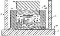
添付の図面を参照して、以下に、本発明の好ましい従来例とは異なる実施例を詳細に説明する。図2は、治工具(tooling device)30を用いて組み立てられた加速度計20の部分断面図である。図示の実施例において、治工具30は、取付構造体(mounting structure)と、ベース34と、側壁36とを含む。取付構造体は、幾つかの例では表面定着物32を研磨する磁極片と呼ばれる得る。加速度計20は、励磁リング(E−リング)頂部ピース40を含み、その上に励磁リング底部ピース42が位置決めされる。治工具30は、加速度計20部品の非常に正確な位置合わせを行う。E−リング頂部ピース40は、その第一端部43に研磨面41を含む。
With reference to the accompanying drawings, a preferred embodiment of the present invention will be described in detail below. FIG. 2 is a partial cross-sectional view of the accelerometer 20 assembled using a tooling device 30. In the illustrated embodiment, the tool 30 includes a mounting structure, a
磁石44がE−リング底部ピース42に取り付けられ、磁極片46が磁石44に取り付けられる。磁石44及び磁極片46は、E−リング底部ピース42から離れて、E−リング頂部ピース40のギャップに向けて上方に延びる。加速度計20は、図2では、逆さまに図示されており、E−リング底部ピース42から離れて下方に延びる磁石44及び磁極片46が図示されている。幾つかの例では、E−リング頂部ピース40はまたE−リング第一ピースと称されることがあり、E−リング底部ピース42はまたE−リング第二ピースと称されることがある。
A magnet 44 is attached to the
一実施例において、E−リングの頂部ピース40及び底部ピース42は、別々に製造されて、加熱処理される。E−リング頂部ピース40は、次いで、少なくとも一面を所定の仕上げ品質にまで粗研磨される。一実施例において、研磨仕上げが研磨面41に施された後、E−リング頂部ピース40は研磨作業からの残留微粒子が取り除かれる。E−リング底部ピース42、磁石44、及び磁極片46は、空気研磨され、E−リングの頂部ピース40、底部ピース42、磁石44、及び磁極片46を含む全ての部品が清浄にされる。その後、加速度計20が組み立てられる。一実施例において、加速度計20の組立ては、HEPAフィルタを用いるなどして、浮遊微小粒子が空気から除去された作業台に、層流の空気が流れる組立て作業台であるクリーン・ベンチ(清浄実験台)を用いて行われる。
In one embodiment, the E-ring
一実施例の組立工程において、磁極片46が表面定着物32を研磨する磁極片中に配置される。次いで、銀充填の第一導電性エポキシ層48[例えば、エイブルスティーク・ラボラトリーズ(Ablestik laboratories)社製のエイブルボンド(登録商標:Ablebond) 84-1LMIT]が、磁極片46に塗布される。次に、表面定着物32を研磨する磁極片中の磁石44を第一エポキシ層48に配置して、磁石44が磁極片46に取り付けられる。次いで、銀充填の第二導電性エポキシ層50(例えば、エイブルスティーク・ラボラトリーズ社製のエイブルボンド 84-1LMIT)が、磁石44に塗布される。
In the assembly process of one embodiment, the pole piece 46 is disposed in the pole piece for polishing the surface fixer 32. A silver-filled first conductive epoxy layer 48 (eg, Ablebond 84-1LMIT from Ablestik laboratories) is then applied to the pole piece 46. Next, the magnet 44 in the pole piece for polishing the surface fixer 32 is disposed on the
次に、E−リング頂部ピース40が、表面定着物32を研磨する磁極片の外側部分49上の治工具30内に配置される。次いで、E−リング底部ピース42が、E−リング頂部ピース40の第二端部51の内側において、エポキシ層50上に配置される。その後、E−リング底部ピース42に力を加える例えば重し又はバネ等の荷重装置52を用いて、表面定着物32を研磨する磁極片に対して、E−リング底部ピース42、磁石44、及び磁極片46を含む堆積物を押圧する。
Next, the E-ring
一実施例において、荷重装置52は、200g以上の重しにより与えられる圧力と同等の圧力を、E−リング底部ピース42に加える。次に、未充填の低粘度エポキシ層(例えば、TRA-CON 社製のTRA-BOND 931-1)54が、E−リング底部ピース42とE−リング頂部ピース40の間に塗布される。TRA-BOND 931-1以外のエポキシ又は他の接着剤も使用できる。かかる代替のエポキシは、典型的には粘度が低いので、E−リング頂部ピース40とE−リング底部ピース42間のギャップを効果的に浸潤する。このような代替のエポキシは、また、典型的にはE−リング頂部ピース40とE−リング底部ピース42を一緒に保持する結合力を有し、時間の経過と共に幾何学的安定性をもたらして、磁気回路に同じ磁束レベルを維持する。
In one embodiment, the load device 52 applies a pressure to the
エポキシ層54の塗布は、例えばE−リング頂部ピース40とE−リング底部ピース42間のギャップに、エポキシ層54を浸潤させることにより実施され得る。エポキシ層48,50,54は、その後、例えば150℃で約1時間加熱することにより硬化される。この例ではエポキシ層48,50,54が同時に硬化されるが、別の例ではエポキシ層を順次又は異なる条件下で硬化してもよい。
Application of the
加速度計20の組立て時における表面定着物32を研磨する磁極片の使用は、表面定着物32を研磨する磁極片の寸法を制御することにより、高い許容誤差に制御され得る表面距離56を研磨する磁極片をもたらす。これは、このようにして製造される異なる加速度計間に一貫性のある表面距離56を研磨する磁極片をもたらし、磁石44の高さ、磁極片46の高さ、第一エポキシ層48の厚さ、及び第二エポキシ層50の厚さの変動を過度に考慮することなく、表面距離56を研磨する磁極片が制御され得るようになる。
The use of pole pieces to polish the surface fixer 32 during assembly of the accelerometer 20 polishes the surface distance 56 that can be controlled to a high tolerance by controlling the size of the pole piece that polishes the surface fixer 32. Bring pole pieces. This results in a pole piece that polishes a consistent surface distance 56 between the different accelerometers manufactured in this manner, the height of the magnet 44, the height of the pole piece 46, the thickness of the
その後、治工具30が取り外され、更なる構成部材が加速度計20に追加されて、図3に図示された構造物を製造する。図2,3は必ずしも縮尺通りに描かれていない。図2,3は加速度計20の種々の部品を断面図で示しているが、当然のことながら部品には体積がある。一実施例の実施の形態では、E−リング頂部ピース40及びE−リング底部ピース42は円筒形である。幾つかの例では、磁石44、磁極片46等の他の構成部材も形状を円筒形にすることができる。
Thereafter, the jig 30 is removed and additional components are added to the accelerometer 20 to produce the structure illustrated in FIG. 2 and 3 are not necessarily drawn to scale. 2 and 3 show various parts of the accelerometer 20 in cross-section, but it should be understood that the parts have volume. In one example embodiment, the E-ring
図3は、治工具30が取り外されて更なる構成部材が追加された後の、図2に示す加速度計20の断面図である。図3は、また、E−リング頂部ピース40が、E−リング底部ピース42の直径62よりも大きい第二端部51に、下部内径60を有することを示している。これにより、図2について説明した組立て時に、E−リング底部ピース42がE−リング頂部ピース40に差し込み可能になる。一実施例において、下部内径60は19.05±0.025mm(0.75±0.001インチ)であり、直径62は18.97±0.025mm(0.747±0.001インチ)であって、径の差が0.076±0.051mm(0.003±0.002インチ)、即ち径の差は、0.076±0.051mm(3±2 mils)又は0.025−0.127mm(between 1 and 5 mils)となる。一実施例において、E−リング底部ピース42は、直径がE−リング頂部ピース40の下部内径よりも約0.076mm(3 mils)小さい。
FIG. 3 is a cross-sectional view of the accelerometer 20 shown in FIG. 2 after the jig 30 has been removed and additional components have been added. FIG. 3 also shows that the E-ring
E−リング頂部ピース40は本実施例では断面がL字形であるが、E−リング頂部ピース40は、別の例では、断面が1又はそれ以上の角部にアールを設けた概ねL字形状等の別の形状であってもよい。更に、E−リング底部ピース42の直径62がE−リング頂部ピース40の下部内径60よりも小さいという条件で、別の大きさの構造を用いることができる。
The E-ring
治工具30が取り外された後に、プルーフ・マス64がE−リング頂部ピース40の上面に追加され、加速度計の電子機器を含むステータ66がプルーフ・マス64の固定部分に取り付けられる。その後、プルーフ・マス64及びステータ66は、例えば腹帯(bellyband)68を用いるなどして、E−リング頂部ピース40に関して所定の位置に保持される。当然のことながら、プルーフ・マス64の外側の剛性部分が、E−リング頂部ピース40に関して所定の位置に保持され、プルーフ・マス64の他の部分が加速度計20の作動時に屈曲するであろう。また、プルーフ・マス64から磁極片46とE−リング頂部ピース40間のギャップに延びる、コイル70が図示されている。
After the jig 30 is removed, a proof mass 64 is added to the top surface of the E-ring
一実施例において、研磨面41は、また、研磨面41とプルーフ・マス64上の金属化プレート(図示せず)との間に形成される、コンデンサの接地板として機能する。また、図2の加速度計部分の鏡像バージョン(version)が、プルーフ・マス64の第二側部に作り出されて取り付けられ、所定の温度範囲にわたって応力及び磁気的挙動の同相モード相殺性能を強めることができる。幾つかの例では、加速度計20の一部又は全ての組立てをクリーン・ルームで行うことができる。 In one embodiment, the polishing surface 41 also functions as a capacitor ground plate formed between the polishing surface 41 and a metallization plate (not shown) on the proof mass 64. Also, a mirror image version of the accelerometer portion of FIG. 2 is created and attached to the second side of the proof mass 64 to enhance the common mode cancellation performance of stress and magnetic behavior over a given temperature range. Can do. In some examples, some or all of the accelerometer 20 can be assembled in a clean room.
本発明の好ましい実施例を図面を用いて説明し記述したが、前述の通り、本発明の精神及び範囲から逸脱することなく多くの変更を行うことができる。例えば、他の種類のエポキシ又はエポキシ以外の種類の接着剤を使用してもよく、幾つかの例では、接着剤の使用以外の取付け方法及び接合方法を採用することができる。更に、片面(single sided)加速度計について説明したが、幾つかの例では、同様の2ピース・励磁リングを用いて両面(double sided)加速度計を形成することもできる。また、表面定着物32を研磨する磁極片を使用する他の種類の治工具も、幾つかの例では使用することができる。 While the preferred embodiment of the invention has been illustrated and described with reference to the drawings, as noted above, many changes can be made without departing from the spirit and scope of the invention. For example, other types of epoxies or types of adhesives other than epoxies may be used, and in some examples, attachment and bonding methods other than the use of adhesives may be employed. Furthermore, although a single sided accelerometer has been described, in some examples, a similar two piece excitation ring can be used to form a double sided accelerometer. Other types of jigs that use pole pieces to polish the surface fixer 32 can also be used in some examples.
加速度計20の組立における異なる工程順序が幾つかの例で行うことができ、又は、例えば、表面定着物32を研磨する磁極片に挿入する前に、磁石44を磁極片46に取り付けるなどして、幾つかの部品を予め組み立てた後に他の部品と結合してもよい。従って、本発明の範囲は、好ましい実施例の開示により限定されるものではない。それよりむしろ、専ら添付の特許請求の範囲を参照して本発明を確定すべきである。 Different process sequences in the assembly of the accelerometer 20 can be performed in some examples, or, for example, by attaching the magnet 44 to the pole piece 46 before inserting the surface fixer 32 into the pole piece to be polished. Some parts may be pre-assembled and then combined with other parts. Accordingly, the scope of the invention is not limited by the disclosure of the preferred embodiment. Instead, the invention should be determined solely by reference to the appended claims.
Claims (3)
第一の内径を第一端部に及び第二の内径を第二端部に有する第一のピース(40)及び第三の直径を有する第二のピース(42)を含み、第三の直径が第二の内径よりも小さく、第一のピースの第二の内径と第二のピースの第三の直径との間に低粘度エポキシ層(54)が塗布され、第一のピースの第一端部に第一の表面が画定される、少なくとも1つの励磁リング、
励磁リングの第二のピースに取り付けられる少なくとも1つの磁石(44)、
少なくとも1つの磁石に取り付けられる少なくとも1つの磁極片(46)であって、磁極片の端部に第二の表面が画定される、磁極片、
プルーフ・マスに取り付けられる少なくとも1つのコイル(70)を含み、
励磁リングの第一のピースが該第一のピースの第一端部におけるギャップを横切る磁極片に隣接し、前記コイルが前記ギャップ内に延びる、加速度計(20)と、
磁極片の第二の表面と第一のピースの第一の表面との間に所定の距離(56)を維持するように、磁極片と励磁リングの第一のピースとを受け入れ、磁極片を励磁リングの第一のピースと位置合わせするように構成される定着物(32)を備える冶工具(30)との組み合わせ。 Proof mass (64),
A first diameter (40) having a first inner diameter at the first end and a second inner diameter at the second end and a second piece (42) having a third diameter, the third diameter There rather smaller than the second inner diameter, low viscosity epoxy layer (54) is applied between the third diameter of the second inner diameter and a second piece of the first piece, the first piece the At least one excitation ring having a first surface defined at one end ;
At least one magnet (44) attached to the second piece of the excitation ring;
At least one pole piece (46) attached to at least one magnet, the pole piece defining a second surface at an end of the pole piece ;
Including at least one coil (70) attached to the proof mass;
An accelerometer (20), wherein a first piece of an excitation ring is adjacent to a pole piece across a gap at a first end of the first piece, and the coil extends into the gap ;
Receiving the pole piece and the first piece of the excitation ring to maintain a predetermined distance (56) between the second surface of the pole piece and the first surface of the first piece; Combination with a tool (30) comprising a fixture (32) configured to align with the first piece of the excitation ring .
The first piece of exciter ring and a belly band (68) attached to the stator further, wherein the first piece of exciter ring, the proof mass, and the stator are held in fixed relation to each other by the belly band. Combination described in.
Applications Claiming Priority (2)
| Application Number | Priority Date | Filing Date | Title |
|---|---|---|---|
| US12/050,854 | 2008-03-18 | ||
| US12/050,854 US7926348B2 (en) | 2008-03-18 | 2008-03-18 | Methods and systems for minimizing vibration rectification error in magnetic circuit accelerometers |
Related Child Applications (1)
| Application Number | Title | Priority Date | Filing Date |
|---|---|---|---|
| JP2014153789A Division JP5774171B2 (en) | 2008-03-18 | 2014-07-29 | Method and system for minimizing vibration rectification errors in a magnetic circuit accelerometer |
Publications (3)
| Publication Number | Publication Date |
|---|---|
| JP2009236911A JP2009236911A (en) | 2009-10-15 |
| JP2009236911A5 JP2009236911A5 (en) | 2014-01-30 |
| JP5591480B2 true JP5591480B2 (en) | 2014-09-17 |
Family
ID=41087577
Family Applications (2)
| Application Number | Title | Priority Date | Filing Date |
|---|---|---|---|
| JP2009063045A Expired - Fee Related JP5591480B2 (en) | 2008-03-18 | 2009-03-16 | Method and system for minimizing vibration rectification errors in a magnetic circuit accelerometer |
| JP2014153789A Expired - Fee Related JP5774171B2 (en) | 2008-03-18 | 2014-07-29 | Method and system for minimizing vibration rectification errors in a magnetic circuit accelerometer |
Family Applications After (1)
| Application Number | Title | Priority Date | Filing Date |
|---|---|---|---|
| JP2014153789A Expired - Fee Related JP5774171B2 (en) | 2008-03-18 | 2014-07-29 | Method and system for minimizing vibration rectification errors in a magnetic circuit accelerometer |
Country Status (2)
| Country | Link |
|---|---|
| US (1) | US7926348B2 (en) |
| JP (2) | JP5591480B2 (en) |
Families Citing this family (10)
| Publication number | Priority date | Publication date | Assignee | Title |
|---|---|---|---|---|
| US8215169B2 (en) * | 2009-03-26 | 2012-07-10 | Honeywell International Inc. | Using pole pieces to guide magnetic flux through a MEMS device and method of making |
| US8649418B1 (en) | 2013-02-08 | 2014-02-11 | CBF Networks, Inc. | Enhancement of the channel propagation matrix order and rank for a wireless channel |
| US9164117B2 (en) * | 2012-10-19 | 2015-10-20 | Honeywell International Inc. | Stress reduction components for sensors |
| US10161956B2 (en) | 2016-04-25 | 2018-12-25 | Honeywell International Inc. | Reducing bias in an accelerometer via a pole piece |
| WO2019118870A1 (en) * | 2017-12-14 | 2019-06-20 | Trak Microwave Corporation | Broadband circulator and method of manufacturing the same |
| CN110806495B (en) * | 2019-10-18 | 2021-06-01 | 中国航空工业集团公司西安飞行自动控制研究所 | High-precision accelerometer pendulum assembly fixture |
| US11422152B2 (en) | 2019-12-10 | 2022-08-23 | Honeywell International Inc. | Stress relieving sensor flange |
| US11169175B2 (en) | 2020-02-11 | 2021-11-09 | Honeywell International Inc. | Multilayer excitation ring |
| US11521772B2 (en) | 2020-02-11 | 2022-12-06 | Honeywell International Inc. | Multilayer magnetic circuit assembly |
| US11275098B2 (en) | 2020-07-14 | 2022-03-15 | Honeywell International Inc. | Accelerometer including rectangular coil and rectangular pole piece |
Family Cites Families (27)
| Publication number | Priority date | Publication date | Assignee | Title |
|---|---|---|---|---|
| US3702073A (en) * | 1969-02-28 | 1972-11-07 | Sundstrand Data Control | Accelerometer |
| US4094199A (en) * | 1976-07-06 | 1978-06-13 | Sundstrand Data Control, Inc. | Accelerometer |
| US4555944A (en) * | 1984-05-01 | 1985-12-03 | Sundstrand Data Control, Inc. | Method and apparatus for producing a controlled preload on a transducer assembly |
| JPS6111666A (en) * | 1984-06-27 | 1986-01-20 | Matsushita Electric Ind Co Ltd | Motion sensor |
| JPH026335Y2 (en) * | 1985-05-24 | 1990-02-15 | ||
| US4726228A (en) * | 1986-04-16 | 1988-02-23 | Sundstrand Data Control, Inc. | Accelerometer proof mass interface |
| JPS633600A (en) * | 1986-06-23 | 1988-01-08 | Minebea Kk | Manufacture of speaker |
| DE3783126T2 (en) * | 1986-06-27 | 1993-05-27 | Sundstrand Corp | FASTENING FOR A PRECISION CONVERTER. |
| JPS6373861A (en) * | 1986-09-11 | 1988-04-04 | Fuji Elelctrochem Co Ltd | Manufacture of magnet circuit |
| JPS6412273A (en) * | 1987-07-06 | 1989-01-17 | Japan Aviation Electron | Magnet construction body in accelerometer |
| US4854169A (en) | 1987-06-15 | 1989-08-08 | Japan Aviation Electronics Industry Ltd. | Accelerometer |
| JPS6448675U (en) * | 1987-09-22 | 1989-03-27 | ||
| JPH0339656A (en) * | 1989-07-06 | 1991-02-20 | Niles Parts Co Ltd | Acceleration sensor |
| US5133214A (en) * | 1990-05-18 | 1992-07-28 | New Sd, Inc. | Adjustment of scale factor linearity in a servo accelerometer |
| US5182949A (en) * | 1991-05-17 | 1993-02-02 | Sundstrand Corporation | Accelerometer with support caging |
| JPH05249136A (en) * | 1992-03-09 | 1993-09-28 | Takata Kk | Acceleration sensor |
| US5557044A (en) * | 1994-01-21 | 1996-09-17 | Alliedsignal, Inc. | Low stress magnet interface |
| JP4054073B2 (en) * | 1994-10-03 | 2008-02-27 | アライドシグナル インコーポレイテッド | Force rebalance accelerometer including a low stress magnet interface. |
| JPH08331690A (en) * | 1995-05-31 | 1996-12-13 | Sony Corp | Speaker, speaker device and manufacture of speaker device |
| JPH1154329A (en) * | 1997-07-31 | 1999-02-26 | Kyocera Corp | Coil type inductor |
| JP2000114062A (en) * | 1998-09-30 | 2000-04-21 | Tokin Corp | Winding parts |
| JP2002058093A (en) * | 2000-08-08 | 2002-02-22 | Kenwood Corp | Loudspeaker and its manufacturing method |
| JP3631461B2 (en) * | 2001-12-04 | 2005-03-23 | 東京コイルエンジニアリング株式会社 | Pot rivet type core choke coil |
| US7194903B2 (en) * | 2004-12-14 | 2007-03-27 | Honeywell International Inc. | Suspension mechanism for high performance accelerometers |
| US7191654B2 (en) * | 2005-08-17 | 2007-03-20 | Honeywell International Inc. | Methods and systems for adjusting magnetic return path with minimized reluctance |
| JP2007336145A (en) * | 2006-06-14 | 2007-12-27 | Pioneer Electronic Corp | Manufacturing method of magnetic circuit for speaker system |
| US20090205424A1 (en) * | 2008-02-15 | 2009-08-20 | Honeywell International Inc. | Flexure type accelerometer and method of making same |
-
2008
- 2008-03-18 US US12/050,854 patent/US7926348B2/en active Active
-
2009
- 2009-03-16 JP JP2009063045A patent/JP5591480B2/en not_active Expired - Fee Related
-
2014
- 2014-07-29 JP JP2014153789A patent/JP5774171B2/en not_active Expired - Fee Related
Also Published As
| Publication number | Publication date |
|---|---|
| US7926348B2 (en) | 2011-04-19 |
| JP5774171B2 (en) | 2015-09-02 |
| JP2009236911A (en) | 2009-10-15 |
| US20090235745A1 (en) | 2009-09-24 |
| JP2014238413A (en) | 2014-12-18 |
Similar Documents
| Publication | Publication Date | Title |
|---|---|---|
| JP5591480B2 (en) | Method and system for minimizing vibration rectification errors in a magnetic circuit accelerometer | |
| US8143083B2 (en) | Physical quantity sensor device and method for producing the same | |
| TWI593048B (en) | Substrate processing system, substrate holder, substrate holder pair, substrate bonding apparatus, and device manufacturing method | |
| JP2007510865A (en) | Test platform for vibration sensitive equipment | |
| JP2009236911A5 (en) | ||
| JP5051021B2 (en) | Electronic component manufacturing apparatus and manufacturing method | |
| JP5504376B2 (en) | Precision spacing for stacked wafer assemblies | |
| JPS63194331A (en) | Mask holding apparatus | |
| JP2007180102A (en) | Suction body and manufacturing method thereof | |
| JP5626993B2 (en) | Method for manufacturing dynamic microphone unit | |
| JP2005158962A (en) | Electrostatic chuck and method for manufacturing the same | |
| JP2004212246A (en) | Acceleration sensor | |
| JP4614581B2 (en) | Fixing jig and fixing method for workpiece | |
| KR102012784B1 (en) | vacuum chuck using a silicon carbide, and manufacturing method thereof | |
| JP6203632B2 (en) | Micro component holding jig | |
| TWI826686B (en) | Load sensor voltage adjustment method | |
| JP6111155B2 (en) | Condenser microphone unit | |
| CN105703594A (en) | Sensing driving module comprising voice coil actuator | |
| JPH0947950A (en) | Prism polishing jig | |
| JP2000018301A (en) | Vibration damping member | |
| US2887877A (en) | Method of testing electromechanical filters | |
| JP2023047558A (en) | Method for manufacturing polishing pad | |
| JP2006269809A (en) | Flat machining method for wafer | |
| JP2015017879A (en) | Electronic device and method for manufacturing the same | |
| JPH09183047A (en) | Sample polishing method |
Legal Events
| Date | Code | Title | Description |
|---|---|---|---|
| A621 | Written request for application examination |
Free format text: JAPANESE INTERMEDIATE CODE: A621 Effective date: 20120313 |
|
| A977 | Report on retrieval |
Free format text: JAPANESE INTERMEDIATE CODE: A971007 Effective date: 20130830 |
|
| A131 | Notification of reasons for refusal |
Free format text: JAPANESE INTERMEDIATE CODE: A131 Effective date: 20130906 |
|
| A524 | Written submission of copy of amendment under section 19 (pct) |
Free format text: JAPANESE INTERMEDIATE CODE: A524 Effective date: 20131205 |
|
| TRDD | Decision of grant or rejection written | ||
| A01 | Written decision to grant a patent or to grant a registration (utility model) |
Free format text: JAPANESE INTERMEDIATE CODE: A01 Effective date: 20140701 |
|
| A61 | First payment of annual fees (during grant procedure) |
Free format text: JAPANESE INTERMEDIATE CODE: A61 Effective date: 20140730 |
|
| R150 | Certificate of patent or registration of utility model |
Ref document number: 5591480 Country of ref document: JP Free format text: JAPANESE INTERMEDIATE CODE: R150 |
|
| LAPS | Cancellation because of no payment of annual fees |