JP5584792B2 - Light source device - Google Patents

Light source device Download PDF

Info

Publication number
JP5584792B2
JP5584792B2 JP2013064883A JP2013064883A JP5584792B2 JP 5584792 B2 JP5584792 B2 JP 5584792B2 JP 2013064883 A JP2013064883 A JP 2013064883A JP 2013064883 A JP2013064883 A JP 2013064883A JP 5584792 B2 JP5584792 B2 JP 5584792B2
Authority
JP
Japan
Prior art keywords
organic
transparent substrate
electrode
layer
transparent
Prior art date
Legal status (The legal status is an assumption and is not a legal conclusion. Google has not performed a legal analysis and makes no representation as to the accuracy of the status listed.)
Expired - Fee Related
Application number
JP2013064883A
Other languages
Japanese (ja)
Other versions
JP2013157327A (en
Inventor
隆雄 宮井
稔 前原
真理 藤本
慎一 安部
良徳 齋藤
容子 松林
Current Assignee (The listed assignees may be inaccurate. Google has not performed a legal analysis and makes no representation or warranty as to the accuracy of the list.)
Panasonic Corp
Panasonic Holdings Corp
Original Assignee
Panasonic Corp
Matsushita Electric Industrial Co Ltd
Priority date (The priority date is an assumption and is not a legal conclusion. Google has not performed a legal analysis and makes no representation as to the accuracy of the date listed.)
Filing date
Publication date
Application filed by Panasonic Corp, Matsushita Electric Industrial Co Ltd filed Critical Panasonic Corp
Priority to JP2013064883A priority Critical patent/JP5584792B2/en
Publication of JP2013157327A publication Critical patent/JP2013157327A/en
Application granted granted Critical
Publication of JP5584792B2 publication Critical patent/JP5584792B2/en
Expired - Fee Related legal-status Critical Current
Anticipated expiration legal-status Critical

Links

Images

Landscapes

  • Electroluminescent Light Sources (AREA)
  • Non-Portable Lighting Devices Or Systems Thereof (AREA)

Description

本発明は、光源装置に関するものである。   The present invention relates to a light source device.

近年、照明用途に用いる光源装置として、線状の有機EL素子が提案されており(例えば、特許文献1,2参照)、上記特許文献1には、図4に示すように、長手方向に直交する断面が円形状であり柔軟性を有する繊維状のコア部材101と、コア部材101の外周面の全周に亘って積層された第1の電極(陰極)102と、第1の電極102の外周面の全周に亘って積層された少なくとも発光層を含む有機層103と、有機層103の外周面の全周に亘って積層された透明導電膜(例えば、ITO膜)からなる第2の電極(陽極)104と、第2の電極104の外周面においてコア部材101の長手方向に沿って形成された断面弧状の金属膜(例えば、Al膜、Cu膜など)からなる低抵抗金属層105と、第2の電極104および低抵抗金属層105に積層されたパッシベーション膜(例えば、SiO膜、Si層膜)からなる水分遮断層106と、水分遮断層106の外周面の全周に亘って積層された透光性封止材(例えば、シリコーン樹脂、エポキシ樹脂など)からなる封止カバー層107とを備えた有機EL素子100が提案されている。 In recent years, a linear organic EL element has been proposed as a light source device used for illumination (see, for example, Patent Documents 1 and 2). In Patent Document 1, as shown in FIG. A fibrous core member 101 having a circular cross section and having flexibility, a first electrode (cathode) 102 laminated over the entire outer periphery of the core member 101, and the first electrode 102 A second layer comprising an organic layer 103 including at least a light-emitting layer laminated over the entire circumference of the outer circumferential surface, and a transparent conductive film (eg, ITO film) laminated over the entire circumference of the outer circumferential surface of the organic layer 103; An electrode (anode) 104 and a low resistance metal layer 105 made of a metal film (for example, an Al film, a Cu film, etc.) having a cross-sectional arc shape formed along the longitudinal direction of the core member 101 on the outer peripheral surface of the second electrode 104. And the second electrode 104 and low resistance The passivation film laminated to the genus layer 105 (eg, SiO 2 film, Si 3 N 4 layer film) and the moisture barrier layer 106 made of, the entire circumference translucent laminated over the outer peripheral surface of the moisture barrier layer 106 An organic EL element 100 including a sealing cover layer 107 made of a sealing material (for example, silicone resin, epoxy resin, etc.) has been proposed.

ここにおいて、図4に示した構成の有機EL素子100では、コア部材101の長手方向の一端部においてシート抵抗の大きな透明導電膜からなる第2の電極104に電気的に接続されたリード線115と第1の電極102に接続されたリード線112との間に直流電源120から直流電圧が印加されるが、第2の電極104の長手方向の全長に亘って低抵抗金属層105を設けてあり、第2の電極104に電気的に接続されるリード線115が低抵抗金属層105を介して第2の電極104に電気的に接続されているので、第2の電極104のシート抵抗による電圧降下に起因した輝度むらが生じるのを抑制することができる。   Here, in the organic EL element 100 having the configuration shown in FIG. 4, the lead wire 115 electrically connected to the second electrode 104 made of a transparent conductive film having a large sheet resistance at one end in the longitudinal direction of the core member 101. A DC voltage is applied from the DC power source 120 between the first electrode 102 and the lead wire 112 connected to the first electrode 102. A low resistance metal layer 105 is provided over the entire length of the second electrode 104 in the longitudinal direction. And the lead wire 115 electrically connected to the second electrode 104 is electrically connected to the second electrode 104 via the low-resistance metal layer 105, so that the sheet resistance of the second electrode 104 depends on the sheet resistance. It is possible to suppress the occurrence of luminance unevenness due to voltage drop.

特開2002−184580号公報JP 2002-184580 A 特開2002−352949号公報JP 2002-352949 A

ところで、上述の有機EL素子100では、製造時に有機層103を例えば蒸着法により成膜する場合、コア部材101を回転させる必要があるが、細長いコア部材101を均一な速度で回転させることが困難であり、第1の電極102の外周面の全周に亘って有機層103を均一に成膜することができず、有機層103からの発光輝度が不均一となってしまい、また、有機層103を例えば塗布法により成膜する場合には、液だれが発生し、第1の電極102の外周面の全周に亘って有機層103を均一に成膜することができず、有機層103からの発光輝度が不均一となってしまう。   By the way, in the organic EL element 100 described above, when the organic layer 103 is formed by vapor deposition, for example, at the time of manufacture, it is necessary to rotate the core member 101, but it is difficult to rotate the elongated core member 101 at a uniform speed. The organic layer 103 cannot be uniformly formed over the entire outer peripheral surface of the first electrode 102, the luminance of light emitted from the organic layer 103 becomes non-uniform, and the organic layer When the film 103 is formed by, for example, a coating method, dripping occurs, and the organic layer 103 cannot be formed uniformly over the entire circumference of the outer peripheral surface of the first electrode 102. The light emission brightness from becomes uneven.

また、上述の有機EL素子100では、当該有機EL素子100を屈曲させた時に有機層103が第1の電極102から剥れやすいという問題があった。なお、上述の有機EL素子100では、当該有機EL素子100を屈曲させた時に封止カバー層107にクラックが発生して、ダークスポットが発生し信頼性が低下するという問題もあった。   Further, the organic EL element 100 described above has a problem that the organic layer 103 is easily peeled off from the first electrode 102 when the organic EL element 100 is bent. Note that the organic EL element 100 described above has a problem that when the organic EL element 100 is bent, a crack is generated in the sealing cover layer 107, a dark spot is generated, and reliability is lowered.

本発明は上記事由に鑑みて為されたものであり、その目的は、発光輝度の均一性を高めることが可能で且つ屈曲時の信頼性の高い光源装置を提供することにある。   The present invention has been made in view of the above reasons, and an object of the present invention is to provide a light source device that can improve the uniformity of light emission luminance and has high reliability when bent.

本発明の光源装置は、有機EL素子を備え、前記有機EL素子は、可撓性を有する帯状の透明基板と、前記透明基板の一表面側において前記透明基板の長手方向に沿って形成された帯状の透明導電膜からなる第1の電極と、前記第1の電極における前記透明基板側とは反対側に形成され少なくとも発光層を含む有機層と、前記有機層における前記第1の電極側とは反対側に形成され前記第1の電極に対向した第2の電極と、前記透明基板の長手方向の一端部に形成され前記第1の電極に電気的に接続された第1の給電部と、前記透明基板の長手方向の他端部に形成され前記第2の電極に電気的に接続された第2の給電部とを備え、前記有機EL素子が前記透明基板の他表面が外周面側となる形で螺旋状に丸められて中空体が形成されてなり、互いに内径の異なる2つの透明カバーにより前記有機EL素子の中空体を挟み込んでいることを特徴とする。   The light source device of the present invention includes an organic EL element, and the organic EL element is formed along a longitudinal direction of the transparent substrate on a flexible strip-shaped transparent substrate and one surface side of the transparent substrate. A first electrode composed of a strip-shaped transparent conductive film; an organic layer formed on the opposite side of the first electrode to the transparent substrate side and including at least a light emitting layer; and the first electrode side of the organic layer; Is formed on the opposite side and is opposed to the first electrode, and is formed at one end in the longitudinal direction of the transparent substrate and is electrically connected to the first electrode. A second power feeding part formed at the other end in the longitudinal direction of the transparent substrate and electrically connected to the second electrode, wherein the organic EL element has the other surface on the outer peripheral surface side A hollow body is formed by being rounded into a spiral shape, Characterized in that sandwich the hollow body of the organic EL element by two transparent cover having different inner diameter are.

この発明によれば、可撓性を有する帯状の透明基板の一表面側に帯状の透明導電膜からなる第1の電極が形成され、第1の電極における透明基板側とは反対側に少なくとも発光層を含む帯状の有機層が形成され、有機層における第1の電極側とは反対側に帯状の第2の電極が形成され、透明基板の他表面が外周面側となる形で螺旋状に丸められて中空体が形成されているので、可撓性を有する帯状の透明基板の一表面側に帯状の透明導電膜からなる第1の電極、少なくとも発光層を含む帯状の有機層、帯状の第2の電極を順次形成してから透明基板を螺旋状に丸めるようにする製造プロセスを採用することができ、製造時に有機層の膜厚均一性を高めることができるから、発光輝度の均一性を高めることができ、しかも、透明基板の他表面が外周面側となる形で螺旋状に丸められて中空体が形成されているので、屈曲時に有機層が第1の電極から剥れるのを防止することができ、屈曲時の信頼性を高めることができる
光源装置において、前記有機EL素子の中空体に外装される前記透明カバーは、内面に接着性を付与してあるのが好ましい。
According to the present invention, the first electrode made of the strip-shaped transparent conductive film is formed on one surface side of the flexible strip-shaped transparent substrate, and at least light emission is performed on the opposite side of the first electrode from the transparent substrate side. A band-shaped organic layer including a layer is formed, a band-shaped second electrode is formed on the opposite side of the organic layer from the first electrode side, and the other surface of the transparent substrate is spirally formed in a shape of the outer peripheral surface side. Since the hollow body is formed by being rounded, the first electrode made of a strip-shaped transparent conductive film on one surface side of the flexible strip-shaped transparent substrate, the strip-shaped organic layer including at least the light-emitting layer, the strip-shaped A manufacturing process in which the second electrode is sequentially formed and then the transparent substrate is rolled up can be employed, and the film thickness uniformity of the organic layer can be increased during manufacturing, so that the uniformity of the light emission luminance is achieved. And the other surface of the transparent substrate Since the hollow body is formed by being spirally wound in the form of the peripheral surface side, the organic layer can be prevented from peeling off from the first electrode during bending, and the reliability during bending can be improved. Can do .
In the light source device, it is preferable that the transparent cover provided on the hollow body of the organic EL element has an adhesive property on an inner surface.

光源装置において、前記中空体は、前記有機EL素子の前記透明基板において並行させる部位間に隙間が生じず且つ前記有機層が重ならないように並行させる部位同士が接着されてなることが好ましい。   In the light source device, it is preferable that the hollow body is formed by adhering the parallel parts so that no gap is generated between the parallel parts of the transparent substrate of the organic EL element and the organic layers do not overlap.

この発明によれば、透明基板において並行させる部位間に隙間が生じず且つ有機層が重ならないように並行させる部位同士が接着されてなるので、透明基板において並行させる部位間に隙間が生じず且つ有機層が重ならない。   According to this invention, the gap between the parallel parts in the transparent substrate does not occur and the parallel parts are bonded so that the organic layers do not overlap. Organic layers do not overlap.

本発明の光源装置では、発光輝度の均一性を高めることが可能で且つ屈曲時の信頼性を高めることができるという効果がある。   In the light source device of the present invention, it is possible to improve the uniformity of light emission luminance and to improve the reliability at the time of bending.

実施形態の光源装置を示し、(a)は概略斜視図、(b)は要部概略平面図、(c)は要部概略断面図である。The light source device of embodiment is shown, (a) is a schematic perspective view, (b) is a principal part schematic plan view, (c) is a principal part schematic sectional drawing. 同上の製造方法の説明図である。It is explanatory drawing of a manufacturing method same as the above. 同上の製造方法の説明図である。It is explanatory drawing of a manufacturing method same as the above. 従来例を示し、(a)は一部破断した概略斜視図、(b)は概略断面図である。A prior art example is shown, (a) is a schematic perspective view partly broken, (b) is a schematic sectional view.

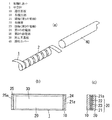
本実施形態の光源装置は、図1(b),(c)に示す帯状の有機EL素子1を同図(a)に示すように螺旋状に丸めて形成された中空体2と、当該中空体2に外装された筒状(本実施形態では、円筒状)の透明カバー40とを備えている。   The light source device of the present embodiment includes a hollow body 2 formed by spirally rolling a strip-shaped organic EL element 1 shown in FIGS. 1B and 1C into a spiral shape as shown in FIG. A cylindrical (in this embodiment, cylindrical) transparent cover 40 is provided on the body 2.

有機EL素子1は、帯状の透明基板10と、透明基板10の一表面側に対向配置された帯状の封止用基板30と、透明基板10と封止用基板30との間に設けられた帯状の有機EL部20とを備え、透明基板10の他表面を光出射面(光取り出し面)としている。なお、有機EL素子1は、無機EL素子に比べて、低電圧、低電流での駆動が可能となり、供給電力に対する発光輝度が大きく、発光効率の良い光源として用いることができる。   The organic EL element 1 is provided between the transparent substrate 10 in a strip shape, the strip-shaped sealing substrate 30 disposed to face one surface of the transparent substrate 10, and the transparent substrate 10 and the sealing substrate 30. The other surface of the transparent substrate 10 is used as a light emitting surface (light extraction surface). In addition, the organic EL element 1 can be driven with a low voltage and a low current as compared with the inorganic EL element, and the light emission luminance with respect to the supplied power is large and can be used as a light source with good light emission efficiency.

ここにおいて、本実施形態では、透明基板10として、可撓性を有する透明な樹脂フィルム基板を用い、透明基板10の厚さを0.1〜0.2mm程度、長手方向の寸法を10〜20cm程度、短手方向の寸法を0.1〜1cm程度としてあるが、これらの数値は特に限定するものではない。   Here, in this embodiment, a transparent resin film substrate having flexibility is used as the transparent substrate 10, the thickness of the transparent substrate 10 is about 0.1 to 0.2 mm, and the dimension in the longitudinal direction is 10 to 20 cm. Although the dimension in the short direction is about 0.1 to 1 cm, these numerical values are not particularly limited.

有機EL部20は、透明基板11の上記一表面上において透明基板11の長手方向に沿って形成された帯状の透明導電膜(例えば、ITO膜など)からなる陽極21であって各辺の寸法が透明基板11よりもやや短い陽極21と、陽極21における透明基板11側とは反対側に形成され少なくとも発光層を含む帯状の有機層22と、有機層22における陽極21側とは反対側に形成され陽極21に対向する帯状の金属膜(例えば、Al膜など)からなる陰極23とを備えている。なお、本実施形態では、陽極21が第1の電極を構成し、陰極が第2の電極を構成している。   The organic EL unit 20 is an anode 21 made of a strip-like transparent conductive film (for example, an ITO film) formed along the longitudinal direction of the transparent substrate 11 on the one surface of the transparent substrate 11, and the dimensions of each side. Is slightly shorter than the transparent substrate 11, the strip-shaped organic layer 22 including at least a light emitting layer formed on the opposite side of the anode 21 to the transparent substrate 11, and the organic layer 22 on the opposite side of the anode 21 side. And a cathode 23 made of a strip-shaped metal film (for example, an Al film) that is formed and faces the anode 21. In the present embodiment, the anode 21 constitutes the first electrode, and the cathode constitutes the second electrode.

有機EL部20は、有機層22における発光層が陽極21と陰極23との間に直流電圧を通電したときに発光するように構成されており、有機層22が、所望の発光色の光が得られる有機分子材料により形成された発光層と、発光層と陽極21との間に介在する正孔輸送層と、発光層と陰極23との間に介在する電子輸送層とを備えている。ここで、有機層22の層構造は特に限定するものではなく、例えば、有機層22の所望の発光色が白色の場合には、発光層中に赤色、緑色、青色の3種類のドーパント色素をドーピングするようにして正孔輸送層と発光層と電子輸送層との積層構造を採用するようにしてもよいし、青色正孔輸送性発光層と緑色電子輸送性発光層と赤色電子輸送性発光層との積層構造を採用してもよいし、正孔輸送層と青色電子輸送性発光層と緑色電子輸送性発光層と赤色電子輸送性発光層との積層構造を採用してもよい。また、透明基板10中に有機層22の発光層からの光によって励起されて発光層からの光に比べて長波長の光を放射する1ないし複数の蛍光体を含有させてもよく、発光層の発光色を青色、蛍光体の発光色を黄色とすれば、白色光を得ることが可能となる。また、有機層22は、正孔輸送層および電子輸送層を設けずに発光層のみにより構成してもよい。   The organic EL unit 20 is configured such that the light emitting layer in the organic layer 22 emits light when a DC voltage is applied between the anode 21 and the cathode 23, and the organic layer 22 emits light of a desired light emitting color. A light emitting layer formed of the obtained organic molecular material, a hole transporting layer interposed between the light emitting layer and the anode 21, and an electron transporting layer interposed between the light emitting layer and the cathode 23 are provided. Here, the layer structure of the organic layer 22 is not particularly limited. For example, when the desired emission color of the organic layer 22 is white, three kinds of dopant dyes of red, green, and blue are added in the emission layer. A laminated structure of a hole transport layer, a light emitting layer, and an electron transport layer may be adopted so as to be doped, or a blue hole transport light emitting layer, a green electron transport light emitting layer, and a red electron transport light emitting layer. A laminated structure with a layer may be employed, or a laminated structure of a hole transporting layer, a blue electron transporting light emitting layer, a green electron transporting light emitting layer, and a red electron transporting light emitting layer may be employed. The transparent substrate 10 may contain one or more phosphors that are excited by light from the light emitting layer of the organic layer 22 and emit light having a longer wavelength than the light from the light emitting layer. If the emission color is blue and the emission color of the phosphor is yellow, white light can be obtained. In addition, the organic layer 22 may be configured by only the light emitting layer without providing the hole transport layer and the electron transport layer.

本実施形態における有機EL素子1は、帯状の陽極21のうち透明基板10の長手方向の一端部上に形成された部位が陽極21に電気的に接続された第1の給電部24を構成しており、透明基板10の長手方向の他端部上に、陰極23に電気的に接続された透明導電膜(例えば、ITO膜など)からなる第2の給電部25が陽極21から離間して形成されている。ここで、第2の給電部25は、短冊状の形状であり、長手方向が陽極21の短手方向に一致する形で形成されている。   The organic EL element 1 in the present embodiment constitutes a first power feeding unit 24 in which a portion formed on one end of the transparent substrate 10 in the longitudinal direction of the strip-shaped anode 21 is electrically connected to the anode 21. On the other end of the transparent substrate 10 in the longitudinal direction, a second power feeding unit 25 made of a transparent conductive film (for example, an ITO film) electrically connected to the cathode 23 is separated from the anode 21. Is formed. Here, the second power supply unit 25 has a strip shape, and is formed such that the longitudinal direction coincides with the short direction of the anode 21.

また、有機EL素子1は、陽極21における1つの長辺と上記一端部側の短辺との2辺に沿って陽極21上に陽極21よりもシート抵抗の小さな第1の低抵抗導電層21aが形成され、第2の給電部25における陽極21から遠い側の長辺に沿って第2の給電部25上に第2の給電部25よりもシート抵抗の小さな第2の低抵抗導電層25aが形成されている。本実施形態の有機EL素子1では、第1の低抵抗導電層21aが陽極21に電気的に接続されているので、各給電部24,25上の低抵抗導電層21a,25a間に直流電圧を印加することにより、透明導電膜からなる陽極21での電圧降下を低減することができる。なお、本実施形態では、給電部24,25と低抵抗導電層21a,25aとで外部接続用端子部を構成している。   Further, the organic EL element 1 includes a first low-resistance conductive layer 21a having a sheet resistance smaller than that of the anode 21 on the anode 21 along two sides of one long side of the anode 21 and the short side on the one end side. The second low-resistance conductive layer 25a having a sheet resistance smaller than that of the second power supply unit 25 is formed on the second power supply unit 25 along the long side farther from the anode 21 in the second power supply unit 25. Is formed. In the organic EL element 1 of the present embodiment, since the first low resistance conductive layer 21a is electrically connected to the anode 21, a direct current voltage is applied between the low resistance conductive layers 21a and 25a on the power feeding units 24 and 25. The voltage drop at the anode 21 made of a transparent conductive film can be reduced. In the present embodiment, the power supply portions 24 and 25 and the low-resistance conductive layers 21a and 25a constitute an external connection terminal portion.

各低抵抗導電層21a,25aは、Al合金膜により構成するようにし、スパッタ法により形成されているが、Al合金膜に限らず、Ti膜とAu膜との積層膜や、Cr膜などにより構成するようにして、スパッタ法により形成するようにしてもよい。なお、各低抵抗導電層21a,25aは、銀ペーストの塗布膜により構成してもよい。   Each of the low resistance conductive layers 21a and 25a is made of an Al alloy film and formed by a sputtering method. However, the low resistance conductive layers 21a and 25a are not limited to the Al alloy film, but are made of a laminated film of a Ti film and an Au film, a Cr film, It may be configured to be formed by sputtering. Each low resistance conductive layer 21a, 25a may be formed of a silver paste coating film.

封止用基板30としては、金属フィルムもしくは樹脂フィルムを用いることが好ましい。また、封止用基板30は、長手方向の一端側において上述の第1の給電部24が露出し且つ長手方向の他端側において上述の第2の給電部25が露出するように、長手方向の寸法を透明基板10よりも短く設定してある。なお、本実施形態では、封止用基板30の厚さを0.1〜0.2mm程度としてあるが、この数値は特に限定するものではない。また、封止用基板30の短手方向の寸法は、透明基板10の短手方向の寸法と同じ値に設定してある。   As the sealing substrate 30, it is preferable to use a metal film or a resin film. In addition, the sealing substrate 30 has a longitudinal direction so that the first power feeding portion 24 is exposed on one end side in the longitudinal direction and the second power feeding portion 25 is exposed on the other end side in the longitudinal direction. Are set shorter than the transparent substrate 10. In the present embodiment, the thickness of the sealing substrate 30 is about 0.1 to 0.2 mm, but this value is not particularly limited. Further, the dimension in the short direction of the sealing substrate 30 is set to the same value as the dimension in the short direction of the transparent substrate 10.

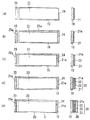
以下、本実施形態の光源装置の製造方法について図2,3に基づいて説明するが、図2(a)〜(e)は、左側の図が概略平面、右側の図が概略断面を示している。   Hereinafter, the manufacturing method of the light source device of the present embodiment will be described with reference to FIGS. 2 and 3. FIGS. 2 (a) to 2 (e) are schematic views on the left side and schematic cross sections on the right side. Yes.

まず、透明基板10の上記一表面上にそれぞれ透明導電膜(例えば、ITO膜など)からなり第1の給電部24を含む陽極21および第2の給電部25を例えばスパッタ法などにより形成することによって、図2(a)に示す構造を得る。   First, the anode 21 and the second power supply unit 25 each made of a transparent conductive film (for example, an ITO film) and including the first power supply unit 24 are formed on the one surface of the transparent substrate 10 by, for example, sputtering. Thus, the structure shown in FIG.

次に、透明基板10の上記一表面側に例えばAl合金膜からなる各低抵抗導電層21a,25aをスパッタ法などにより形成することによって、図2(b)に示す構造を得る。   Next, the low resistance conductive layers 21a and 25a made of, for example, an Al alloy film are formed on the one surface side of the transparent substrate 10 by sputtering or the like, thereby obtaining the structure shown in FIG.

その後、透明基板10の上記一表面側に、有機層22を例えば蒸着法などにより形成することによって、図2(c)に示す構造を得る。なお、有機層22の形成方法は蒸着法に限らず、例えば、塗布法などでもよく、有機層22の有機分子材料に応じて適宜選択すればよい。   Then, the structure shown in FIG. 2C is obtained by forming the organic layer 22 on the one surface side of the transparent substrate 10 by, for example, vapor deposition. In addition, the formation method of the organic layer 22 is not limited to the vapor deposition method, and may be a coating method, for example, and may be appropriately selected according to the organic molecular material of the organic layer 22.

続いて、透明基板10の上記一表面側に、金属膜(例えば、Al膜など)からなる陰極23をスパッタ法などにより形成することによって、図2(d)に示す構造を得る。   Subsequently, a cathode 23 made of a metal film (for example, an Al film) is formed on the one surface side of the transparent substrate 10 by a sputtering method or the like, thereby obtaining the structure shown in FIG.

その後、透明基板10の上記一表面側に、有機EL部20を封止する封止用基板30を接着することによって、図2(e)に示す構造の有機EL素子1を得る。なお、図2では有機EL部20が透明基板10よりも厚く描いてあるが、実際には有機EL部20の厚みは例えば1μm程度であるのに対して、透明基板10および封止用基板30の厚みは0.1〜0.2mm程度であり、封止用基板30の外周部の大部分は透明基板10に接着される。   Then, the organic EL element 1 having the structure shown in FIG. 2E is obtained by adhering a sealing substrate 30 for sealing the organic EL portion 20 to the one surface side of the transparent substrate 10. In FIG. 2, the organic EL portion 20 is drawn thicker than the transparent substrate 10, but the thickness of the organic EL portion 20 is actually about 1 μm, for example, whereas the transparent substrate 10 and the sealing substrate 30 are Is approximately 0.1 to 0.2 mm, and most of the outer peripheral portion of the sealing substrate 30 is bonded to the transparent substrate 10.

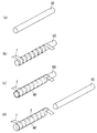
その後、図3(a)に示すような丸棒状の芯棒50を用意し、同図(b)に示すように有機EL素子1を透明基板10の上記他表面が外周面側となる形で芯棒50の外周面に螺旋状に巻回し、その後、有機EL素子1の両端部を固定した状態で同図(c)に示すように有機EL素子1の外周面側に円筒状の透明カバー40を外装して有機EL素子1の両端部を透明カバー50から露出させ、続いて、同図(d)に示すように有機EL素子1から芯棒50を抜くことにより、図1(a)に示す構造の光源装置が完成する。なお、本実施形態では、透明カバー40として、内面に接着性を付与してあるので、透明カバー40を有機EL素子1の中空体2に外装させることにより、透明カバー40と有機EL素子1における透明基板10の上記他表面とが接着されるから、有機EL素子1を保護することができるとともに、有機EL素子1の巻き戻りが生じないようになっている。   Thereafter, a round bar-shaped core rod 50 as shown in FIG. 3A is prepared. As shown in FIG. 3B, the organic EL element 1 is formed such that the other surface of the transparent substrate 10 is on the outer peripheral surface side. A cylindrical transparent cover is formed on the outer peripheral surface side of the organic EL element 1 as shown in FIG. 2C with the both ends of the organic EL element 1 fixed in a spiral manner around the outer peripheral surface of the core rod 50. 40, the both ends of the organic EL element 1 are exposed from the transparent cover 50, and then the core rod 50 is removed from the organic EL element 1 as shown in FIG. The light source device having the structure shown in FIG. In addition, in this embodiment, since adhesiveness is provided to the inner surface as the transparent cover 40, the transparent cover 40 and the organic EL element 1 are covered with the hollow cover 2 of the organic EL element 1. Since the other surface of the transparent substrate 10 is bonded, the organic EL element 1 can be protected and the organic EL element 1 is not rewound.

なお、有機EL素子1を巻回する際には、透明基板10において並行させる部位の間隔を小さくするように巻回することが望ましく、透明基板10において並行させる部位間に隙間が生じず且つ有機層22が重ならないように並行させる部位同士を接着しながら巻回することがより望ましい。また、互いに内径の異なる透明カバー40を2つ用いて有機EL素子1を挟み込んでもよい。また、本実施形態の光源装置は、透明カバー40に部分的に穴を設けることで、屈曲しやすくさせることもできる。   In addition, when winding the organic EL element 1, it is desirable to wind so that the space | interval of the site | part paralleled in the transparent substrate 10 may be made small, and a clearance gap does not arise between the site | parts paralleled in the transparent substrate 10, and organic It is more desirable to wind while adhering the parallel parts so that the layers 22 do not overlap. Further, the organic EL element 1 may be sandwiched between two transparent covers 40 having different inner diameters. Moreover, the light source device of this embodiment can be easily bent by providing a hole in the transparent cover 40 partially.

以上説明した本実施形態の光源装置は、可撓性を有する帯状の透明基板10と、透明基板10の上記一表面側において透明基板10の長手方向に沿って形成された帯状の透明導電膜からなる陽極21と、陽極21における透明基板10側とは反対側に形成され少なくとも発光層を含む帯状の有機層22と、有機層22における陽極21側とは反対側に形成され陽極21に対向した帯状の陰極21と、透明基板10の長手方向の一端部に形成され陽極21に電気的に接続された第1の給電部24と、透明基板10の長手方向の他端部に形成され陰極23に電気的に接続された第2の給電部25とを備え、透明基板10の他表面が外周面側となる形で螺旋状に丸められて中空体2が形成されているので、可撓性を有する帯状の透明基板10の上記一表面側に、帯状の透明導電膜からなる陽極21、少なくとも発光層を含む帯状の有機層22、帯状の陰極23を順次形成してから透明基板10を螺旋状に丸めるようにする製造プロセスを採用することができるので、製造時に有機層22の膜厚均一性を高めることができるから、発光輝度の均一性を高めることができ、しかも、透明基板10の他表面が外周面側となる形で螺旋状に丸められて中空体2が形成されているので、屈曲時に有機層22が陽極21から剥れるのを防止することができ、屈曲時の信頼性を高めることができる。したがって、3次元形状の自由度の高いフレキシブルな光源装置として利用することができる。また、透明基板10の長手方向の一端部に第1の給電部24が形成され、他端部に第2の給電部25が形成されているので、外部の電源などとの電気的な接続が容易になる。なお、本実施形態の有機EL素子1では、給電部24,25を帯状の透明基板10の短手方向に沿った2辺近傍に露出させてあるが、長手方向に沿った2辺近傍に露出させてもよいし、透明基板10の4辺近傍に露出させるようにしてもよい。また、光源装置を屈曲させて曲線形状を維持させるために、後から中空体2に金属棒を挿入してもよい。   The light source device of this embodiment described above includes a flexible strip-shaped transparent substrate 10 and a strip-shaped transparent conductive film formed along the longitudinal direction of the transparent substrate 10 on the one surface side of the transparent substrate 10. Formed on the opposite side of the anode 21 from the transparent substrate 10 side and including at least the light-emitting layer, and formed on the opposite side of the organic layer 22 from the anode 21 side and opposed to the anode 21. A strip-shaped cathode 21, a first power feeding portion 24 formed at one end portion in the longitudinal direction of the transparent substrate 10 and electrically connected to the anode 21, and a cathode 23 formed at the other end portion in the longitudinal direction of the transparent substrate 10. And the second power feeding portion 25 electrically connected to the outer surface of the transparent substrate 10, and the hollow body 2 is formed by being rounded spirally so that the other surface of the transparent substrate 10 is on the outer peripheral surface side. The band-shaped transparent substrate 10 having A manufacturing process is adopted in which an anode 21 made of a strip-shaped transparent conductive film, a strip-shaped organic layer 22 including at least a light-emitting layer, and a strip-shaped cathode 23 are sequentially formed on the surface side, and then the transparent substrate 10 is rolled up spirally Since the thickness uniformity of the organic layer 22 can be increased during manufacturing, the uniformity of the light emission luminance can be increased, and the other surface of the transparent substrate 10 is on the outer peripheral surface side. Since the hollow body 2 is formed by being spirally wound, the organic layer 22 can be prevented from peeling off from the anode 21 at the time of bending, and the reliability at the time of bending can be improved. Therefore, it can be used as a flexible light source device having a high degree of freedom in a three-dimensional shape. In addition, since the first power supply unit 24 is formed at one end in the longitudinal direction of the transparent substrate 10 and the second power supply unit 25 is formed at the other end, electrical connection with an external power source or the like is possible. It becomes easy. In the organic EL element 1 of the present embodiment, the power feeding portions 24 and 25 are exposed in the vicinity of two sides along the short direction of the strip-shaped transparent substrate 10, but are exposed in the vicinity of two sides along the longitudinal direction. Alternatively, it may be exposed near the four sides of the transparent substrate 10. Moreover, in order to bend the light source device and maintain the curved shape, a metal rod may be inserted into the hollow body 2 later.

本実施形態では、第1の電極が陽極21により構成され、第2の電極が陰極23により構成されているが、陽極21と陰極23との配置および材料を逆にして、陰極23が第1の電極を構成し陽極21が第2の電極を構成するようにしてもよい。   In the present embodiment, the first electrode is constituted by the anode 21 and the second electrode is constituted by the cathode 23. However, the arrangement and materials of the anode 21 and the cathode 23 are reversed, and the cathode 23 is the first. The anode 21 may constitute the second electrode.

1 有機EL素子
2 中空体
10 透明基板
20 有機EL部
21 陽極(第1の電極)
22 有機層
23 陰極(第2の電極)
24 第1の給電部
25 第2の給電部
30 封止用基板
40 透明カバー
DESCRIPTION OF SYMBOLS 1 Organic EL element 2 Hollow body 10 Transparent substrate 20 Organic EL part 21 Anode (1st electrode)
22 Organic layer 23 Cathode (second electrode)
24 1st electric power feeding part 25 2nd electric power feeding part 30 Substrate for sealing 40 Transparent cover

Claims (3)

有機EL素子を備え、前記有機EL素子は、可撓性を有する帯状の透明基板と、前記透明基板の一表面側において前記透明基板の長手方向に沿って形成された帯状の透明導電膜からなる第1の電極と、前記第1の電極における前記透明基板側とは反対側に形成され少なくとも発光層を含む有機層と、前記有機層における前記第1の電極側とは反対側に形成され前記第1の電極に対向した第2の電極と、前記透明基板の長手方向の一端部に形成され前記第1の電極に電気的に接続された第1の給電部と、前記透明基板の長手方向の他端部に形成され前記第2の電極に電気的に接続された第2の給電部とを備え、前記有機EL素子が前記透明基板の他表面が外周面側となる形で螺旋状に丸められて中空体が形成されてなり、互いに内径の異なる2つの透明カバーにより前記有機EL素子の中空体を挟み込んでいることを特徴とする光源装置。   The organic EL element comprises a flexible strip-shaped transparent substrate and a strip-shaped transparent conductive film formed along the longitudinal direction of the transparent substrate on one surface side of the transparent substrate. A first electrode; an organic layer formed on a side opposite to the transparent substrate side of the first electrode and including at least a light emitting layer; and a side of the organic layer opposite to the first electrode side A second electrode opposed to the first electrode; a first feeding portion formed at one end of the transparent substrate in the longitudinal direction and electrically connected to the first electrode; and a longitudinal direction of the transparent substrate A second power feeding portion formed on the other end of the substrate and electrically connected to the second electrode, wherein the organic EL element is spirally shaped such that the other surface of the transparent substrate is on the outer peripheral surface side. A hollow body is formed by rounding, and the inner diameters are different from each other. Light source device characterized by a transparent cover sandwiches the hollow body of the organic EL element. 前記有機EL素子の中空体に外装される前記透明カバーは、内面に接着性を付与してあることを特徴とする請求項1記載の光源装置 The light source device according to claim 1 , wherein the transparent cover that is sheathed by the hollow body of the organic EL element has an inner surface provided with adhesiveness . 前記中空体は、前記有機EL素子の前記透明基板において並行させる部位間に隙間が生じず且つ前記有機層が重ならないように並行させる部位同士が接着されてなることを特徴とする請求項1又は2記載の光源装置。The hollow body is formed by adhering parallel parts so that no gap is generated between the parallel parts of the transparent substrate of the organic EL element and the organic layers do not overlap. 2. The light source device according to 2.
JP2013064883A 2013-03-26 2013-03-26 Light source device Expired - Fee Related JP5584792B2 (en)

Priority Applications (1)

Application Number Priority Date Filing Date Title
JP2013064883A JP5584792B2 (en) 2013-03-26 2013-03-26 Light source device

Applications Claiming Priority (1)

Application Number Priority Date Filing Date Title
JP2013064883A JP5584792B2 (en) 2013-03-26 2013-03-26 Light source device

Related Parent Applications (1)

Application Number Title Priority Date Filing Date
JP2007237058A Division JP2009070995A (en) 2007-09-12 2007-09-12 Light source device

Publications (2)

Publication Number Publication Date
JP2013157327A JP2013157327A (en) 2013-08-15
JP5584792B2 true JP5584792B2 (en) 2014-09-03

Family

ID=49052262

Family Applications (1)

Application Number Title Priority Date Filing Date
JP2013064883A Expired - Fee Related JP5584792B2 (en) 2013-03-26 2013-03-26 Light source device

Country Status (1)

Country Link
JP (1) JP5584792B2 (en)

Families Citing this family (1)

* Cited by examiner, † Cited by third party
Publication number Priority date Publication date Assignee Title
JPWO2015118919A1 (en) * 2014-02-10 2017-03-23 コニカミノルタ株式会社 Organic electroluminescence lighting device

Family Cites Families (7)

* Cited by examiner, † Cited by third party
Publication number Priority date Publication date Assignee Title
JPS5912063Y2 (en) * 1979-08-30 1984-04-12 日本電気ホームエレクトロニクス株式会社 electroluminescent lamp
IL104052A (en) * 1992-12-10 1996-07-23 Elam Electroluminescent Ind Lt Electroluminescent light sources
JP2000243553A (en) * 1999-02-19 2000-09-08 Ebakku:Kk Light emitting tube
US6538375B1 (en) * 2000-08-17 2003-03-25 General Electric Company Oled fiber light source
US6787990B2 (en) * 2002-05-28 2004-09-07 Eastman Kodak Company OLED area illumination light source having flexible substrate on a support
JP4474884B2 (en) * 2003-09-29 2010-06-09 セイコーエプソン株式会社 Organic EL device
GB0407230D0 (en) * 2004-03-30 2004-05-05 Koninkl Philips Electronics Nv Fibre or filament with lateral electric fields

Also Published As

Publication number Publication date
JP2013157327A (en) 2013-08-15

Similar Documents

Publication Publication Date Title
US8421064B2 (en) Organic-light-emitting-diode flat-panel light-source apparatus
WO2010098392A1 (en) Planar light emitting device
JP5854746B2 (en) Top emission type organic electroluminescence light emitting device and manufacturing method thereof
WO2011155306A1 (en) Organic electroluminescent illumination device
JP4474884B2 (en) Organic EL device
EP2276088A3 (en) Light emitting element and manufacturing method thereof, and light emitting device using the light emitting element
JP2011192544A5 (en)
US10553832B2 (en) Lighting apparatus using organic light emitting device and method of fabricating thereof
KR102321663B1 (en) Lighting apparatus using organic light emitting diode and method of fabricating thereof
KR20140041922A (en) Light emitting device
US20110084253A1 (en) Organic light emitting diode lighting apparatus and method for manufacturing the same
CN108172598A (en) Lighting Equipment Using Organic Light Emitting Diodes
JP4533963B2 (en) Organic EL light emitting device
JP5584792B2 (en) Light source device
CN109244265B (en) Organic light-emitting diode and method of making the same
CN104145530B (en) Manufacturing method of organic EL element and organic EL element
JP5102570B2 (en) Light source device
JP2009070995A (en) Light source device
JP2009259435A (en) Organic el element
KR20170063593A (en) Organic el panel and method for producing same
KR101403407B1 (en) Organic Light Emitting Diodes Flat Panel Light Source Apparatus and Method Manufacturing the Same
CN103730599B (en) Organic light emitting diode lighting device and manufacturing method thereof
WO2013179482A1 (en) Organic el light-emitting element and method for manufacturing same
CN103311077B (en) Fluorescent illuminating device and phosphor layer formation method thereof
US20140111084A1 (en) Oled lighting device

Legal Events

Date Code Title Description
A977 Report on retrieval

Free format text: JAPANESE INTERMEDIATE CODE: A971007

Effective date: 20131127

A131 Notification of reasons for refusal

Free format text: JAPANESE INTERMEDIATE CODE: A131

Effective date: 20140128

A521 Request for written amendment filed

Free format text: JAPANESE INTERMEDIATE CODE: A523

Effective date: 20140331

TRDD Decision of grant or rejection written
A01 Written decision to grant a patent or to grant a registration (utility model)

Free format text: JAPANESE INTERMEDIATE CODE: A01

Effective date: 20140624

A61 First payment of annual fees (during grant procedure)

Free format text: JAPANESE INTERMEDIATE CODE: A61

Effective date: 20140718

R151 Written notification of patent or utility model registration

Ref document number: 5584792

Country of ref document: JP

Free format text: JAPANESE INTERMEDIATE CODE: R151

LAPS Cancellation because of no payment of annual fees