JP4533963B2 - Organic EL light emitting device - Google Patents
Organic EL light emitting device Download PDFInfo
- Publication number
- JP4533963B2 JP4533963B2 JP2009090083A JP2009090083A JP4533963B2 JP 4533963 B2 JP4533963 B2 JP 4533963B2 JP 2009090083 A JP2009090083 A JP 2009090083A JP 2009090083 A JP2009090083 A JP 2009090083A JP 4533963 B2 JP4533963 B2 JP 4533963B2
- Authority
- JP
- Japan
- Prior art keywords
- layer
- organic
- electrode
- light emitting
- electrode layer
- Prior art date
- Legal status (The legal status is an assumption and is not a legal conclusion. Google has not performed a legal analysis and makes no representation as to the accuracy of the status listed.)
- Expired - Fee Related
Links
- 239000010410 layer Substances 0.000 claims description 340
- 239000012044 organic layer Substances 0.000 claims description 42
- 239000011368 organic material Substances 0.000 claims description 31
- 238000005401 electroluminescence Methods 0.000 description 145
- 230000004048 modification Effects 0.000 description 64
- 238000012986 modification Methods 0.000 description 64
- 239000000758 substrate Substances 0.000 description 35
- 238000010586 diagram Methods 0.000 description 29
- 229910052751 metal Inorganic materials 0.000 description 22
- 239000002184 metal Substances 0.000 description 22
- 239000000463 material Substances 0.000 description 17
- 238000007789 sealing Methods 0.000 description 15
- 230000002093 peripheral effect Effects 0.000 description 11
- 238000000605 extraction Methods 0.000 description 9
- 238000000034 method Methods 0.000 description 9
- 238000002347 injection Methods 0.000 description 7
- 239000007924 injection Substances 0.000 description 7
- 239000011241 protective layer Substances 0.000 description 7
- 238000004519 manufacturing process Methods 0.000 description 5
- 239000010409 thin film Substances 0.000 description 5
- 239000002585 base Substances 0.000 description 4
- 239000010408 film Substances 0.000 description 4
- 239000000126 substance Substances 0.000 description 4
- OKTJSMMVPCPJKN-UHFFFAOYSA-N Carbon Chemical compound [C] OKTJSMMVPCPJKN-UHFFFAOYSA-N 0.000 description 3
- XUIMIQQOPSSXEZ-UHFFFAOYSA-N Silicon Chemical compound [Si] XUIMIQQOPSSXEZ-UHFFFAOYSA-N 0.000 description 3
- 229910001413 alkali metal ion Inorganic materials 0.000 description 3
- 229910052782 aluminium Inorganic materials 0.000 description 3
- XAGFODPZIPBFFR-UHFFFAOYSA-N aluminium Chemical compound [Al] XAGFODPZIPBFFR-UHFFFAOYSA-N 0.000 description 3
- 239000002041 carbon nanotube Substances 0.000 description 3
- 229910021393 carbon nanotube Inorganic materials 0.000 description 3
- 239000002274 desiccant Substances 0.000 description 3
- 239000002159 nanocrystal Substances 0.000 description 3
- 230000002265 prevention Effects 0.000 description 3
- 229910052710 silicon Inorganic materials 0.000 description 3
- 239000010703 silicon Substances 0.000 description 3
- ATJFFYVFTNAWJD-UHFFFAOYSA-N Tin Chemical compound [Sn] ATJFFYVFTNAWJD-UHFFFAOYSA-N 0.000 description 2
- 239000006185 dispersion Substances 0.000 description 2
- 229920001971 elastomer Polymers 0.000 description 2
- 239000000806 elastomer Substances 0.000 description 2
- 230000020169 heat generation Effects 0.000 description 2
- 230000005525 hole transport Effects 0.000 description 2
- AMGQUBHHOARCQH-UHFFFAOYSA-N indium;oxotin Chemical compound [In].[Sn]=O AMGQUBHHOARCQH-UHFFFAOYSA-N 0.000 description 2
- 239000011261 inert gas Substances 0.000 description 2
- 125000002080 perylenyl group Chemical group C1(=CC=C2C=CC=C3C4=CC=CC5=CC=CC(C1=C23)=C45)* 0.000 description 2
- CSHWQDPOILHKBI-UHFFFAOYSA-N peryrene Natural products C1=CC(C2=CC=CC=3C2=C2C=CC=3)=C3C2=CC=CC3=C1 CSHWQDPOILHKBI-UHFFFAOYSA-N 0.000 description 2
- 239000005361 soda-lime glass Substances 0.000 description 2
- 229910052718 tin Inorganic materials 0.000 description 2
- RYGMFSIKBFXOCR-UHFFFAOYSA-N Copper Chemical compound [Cu] RYGMFSIKBFXOCR-UHFFFAOYSA-N 0.000 description 1
- 229910004298 SiO 2 Inorganic materials 0.000 description 1
- VYPSYNLAJGMNEJ-UHFFFAOYSA-N Silicium dioxide Chemical compound O=[Si]=O VYPSYNLAJGMNEJ-UHFFFAOYSA-N 0.000 description 1
- BQCADISMDOOEFD-UHFFFAOYSA-N Silver Chemical compound [Ag] BQCADISMDOOEFD-UHFFFAOYSA-N 0.000 description 1
- RTAQQCXQSZGOHL-UHFFFAOYSA-N Titanium Chemical compound [Ti] RTAQQCXQSZGOHL-UHFFFAOYSA-N 0.000 description 1
- HCHKCACWOHOZIP-UHFFFAOYSA-N Zinc Chemical compound [Zn] HCHKCACWOHOZIP-UHFFFAOYSA-N 0.000 description 1
- 230000003321 amplification Effects 0.000 description 1
- 239000003990 capacitor Substances 0.000 description 1
- 239000003086 colorant Substances 0.000 description 1
- 229910052802 copper Inorganic materials 0.000 description 1
- 239000010949 copper Substances 0.000 description 1
- 230000003247 decreasing effect Effects 0.000 description 1
- 230000007547 defect Effects 0.000 description 1
- 238000001514 detection method Methods 0.000 description 1
- 239000002019 doping agent Substances 0.000 description 1
- 239000000975 dye Substances 0.000 description 1
- 230000005684 electric field Effects 0.000 description 1
- 239000011521 glass Substances 0.000 description 1
- PCHJSUWPFVWCPO-UHFFFAOYSA-N gold Chemical compound [Au] PCHJSUWPFVWCPO-UHFFFAOYSA-N 0.000 description 1
- 229910052737 gold Inorganic materials 0.000 description 1
- 239000010931 gold Substances 0.000 description 1
- 229910052738 indium Inorganic materials 0.000 description 1
- APFVFJFRJDLVQX-UHFFFAOYSA-N indium atom Chemical compound [In] APFVFJFRJDLVQX-UHFFFAOYSA-N 0.000 description 1
- 229910003437 indium oxide Inorganic materials 0.000 description 1
- PJXISJQVUVHSOJ-UHFFFAOYSA-N indium(iii) oxide Chemical compound [O-2].[O-2].[O-2].[In+3].[In+3] PJXISJQVUVHSOJ-UHFFFAOYSA-N 0.000 description 1
- 239000012212 insulator Substances 0.000 description 1
- 239000002346 layers by function Substances 0.000 description 1
- 150000004767 nitrides Chemical class 0.000 description 1
- 238000003199 nucleic acid amplification method Methods 0.000 description 1
- 239000005416 organic matter Substances 0.000 description 1
- 230000010355 oscillation Effects 0.000 description 1
- 229910052814 silicon oxide Inorganic materials 0.000 description 1
- 229910052709 silver Inorganic materials 0.000 description 1
- 239000004332 silver Substances 0.000 description 1
- 239000010936 titanium Substances 0.000 description 1
- 229910052719 titanium Inorganic materials 0.000 description 1
- 239000012780 transparent material Substances 0.000 description 1
- 229910052725 zinc Inorganic materials 0.000 description 1
- 239000011701 zinc Substances 0.000 description 1
Images


Description
本発明は有機EL発光装置、有機EL照明装置および有機EL発光装置の電流注入方法に関し、特に、内面に有機EL発光素子を形成した円筒型有機EL発光装置に電流を供給するための有機EL発光装置、有機EL照明装置および有機EL発光装置の電流注入方法に関するものである。 The present invention relates to an organic EL light emitting device, an organic EL lighting device, and a current injection method for the organic EL light emitting device, and in particular, organic EL light emission for supplying current to a cylindrical organic EL light emitting device having an organic EL light emitting element formed on the inner surface. The present invention relates to a current injection method for an apparatus, an organic EL lighting device, and an organic EL light emitting device.
近年、有機EL(Electro Luminescence)素子が形成された円筒型の面発光デバイスが提案されている。たとえば特開2007−73403号公報(特許文献1)によれば、面発光デバイスは、円筒形状の透明基材(管)と、この透明基材に形成された有機EL素子とを備えている。有機EL素子は、管の内側に順番に成膜された透明電極と、有機EL層と、金属電極とを有している。透明電極は、金属薄膜、インジウム、亜鉛、錫のいずれかの酸化物、またはチタンの窒化物が用いられている。金属電極は、アルミニウム、金、銀、銅などが用いられている。 In recent years, a cylindrical surface emitting device in which an organic EL (Electro Luminescence) element is formed has been proposed. For example, according to Japanese Patent Application Laid-Open No. 2007-73403 (Patent Document 1), a surface emitting device includes a cylindrical transparent base material (tube) and an organic EL element formed on the transparent base material. The organic EL element has a transparent electrode, an organic EL layer, and a metal electrode that are sequentially formed inside the tube. As the transparent electrode, a metal thin film, an oxide of any one of indium, zinc and tin, or a nitride of titanium is used. As the metal electrode, aluminum, gold, silver, copper, or the like is used.
また、たとえば特開2003−142252号公報(特許文献2)には、筒状の非透湿性透明基板(管)と、この内周面に形成された有機EL素子とを備えている管状発光装置が開示されている。有機EL素子は、陽電極層、発光機能層および陰電極層からなる。陽電極層は仕事関数の大きい金属から形成され、陰電極層は仕事関数の小さい金属から形成されることが開示されている。 Further, for example, in Japanese Patent Application Laid-Open No. 2003-142252 (Patent Document 2), a tubular light emitting device including a tubular non-moisture permeable transparent substrate (tube) and an organic EL element formed on the inner peripheral surface thereof. Is disclosed. The organic EL element includes a positive electrode layer, a light emitting functional layer, and a negative electrode layer. It is disclosed that the positive electrode layer is formed from a metal having a high work function, and the negative electrode layer is formed from a metal having a low work function.
この有機EL素子は、ダイオードの特性を有し、透明電極および金属電極に電圧を印加して電流を注入することにより発光するデバイスである。つまり、有機EL素子は、一般的には直流電流を供給することで発光する。 This organic EL element has a diode characteristic and emits light when a voltage is applied to a transparent electrode and a metal electrode to inject a current. That is, the organic EL element generally emits light by supplying a direct current.
上記特許文献1および2に開示のデバイスでは、管の長手方向において発光輝度にばらつきが生じるという問題があった。また、この問題に対して上記特許文献1および2では何らの工夫もされていなかった。
The devices disclosed in
本発明は、上記課題を鑑みてなされたものであり、その目的は、発光輝度のばらつきを抑制する有機EL発光装置、有機EL照明装置および有機EL発光装置の電流注入方法を提供することである。 The present invention has been made in view of the above problems, and an object thereof is to provide an organic EL light-emitting device, an organic EL lighting device, and a current injection method for the organic EL light-emitting device that suppress variation in light emission luminance. .
本発明の有機EL発光装置は、管と、第1電極層と、有機物層と、第2電極層とを備えている。管は、透光性を有している。第1電極層は、管の内側に管の延びる方向に沿って形成され、透光性を有している。有機物層は、第1電極層の内側に管の延びる方向に沿って形成され、電圧が印加されることにより発光する。第2電極層は、有機物層の内側に管の延びる方向に沿って形成されている。第1電極層および第2電極層のいずれか一方が陽極で、他方が陰極である。第1電極層の電気抵抗値と第2電極層の電気抵抗値とは同じである。 The organic EL light emitting device of the present invention includes a tube, a first electrode layer, an organic material layer, and a second electrode layer. The tube has translucency. The first electrode layer is formed inside the tube along the direction in which the tube extends, and has translucency. The organic material layer is formed inside the first electrode layer along the direction in which the tube extends, and emits light when a voltage is applied. The second electrode layer is formed inside the organic layer along the direction in which the tube extends. One of the first electrode layer and the second electrode layer is an anode, and the other is a cathode. The electrical resistance value of the first electrode layer and the electrical resistance value of the second electrode layer are the same.
本発明の有機EL発光装置によれば、第1および第2電極層の延びる方向に沿う単位長さ当たりの電気抵抗値が同一である。このため、第1電極層および第2電極層のいずれか一方の陽極に電流を供給し、他方の陰極から電流を取り出すと、第1電極層および第2電極層の延びる方向に沿った互いに対向する位置において同一の電圧降下が生じる。つまり、管の長手方向に沿った第1電極層および第2電極層との電位差が同一になる。このため、第1電極層および第2電極層から有機物層に管の長手方向に沿って均一な電流を流すことができる。したがって、発光輝度のばらつきを抑制することができる。 According to the organic EL light emitting device of the present invention, the electric resistance value per unit length along the extending direction of the first and second electrode layers is the same. For this reason, when a current is supplied to one of the anodes of the first electrode layer and the second electrode layer and a current is taken out from the other cathode, they face each other along the extending direction of the first electrode layer and the second electrode layer. The same voltage drop occurs at the position where That is, the potential difference between the first electrode layer and the second electrode layer along the longitudinal direction of the tube is the same. For this reason, a uniform electric current can be sent along the longitudinal direction of the tube from the first electrode layer and the second electrode layer to the organic layer. Therefore, variation in light emission luminance can be suppressed.
なお、上記「第1電極層の電気抵抗値と第2電極層の電気抵抗値とは同じ」とは、第1電極層の電気抵抗値と第2電極層の電気抵抗値とは、数値が完全に同一である場合と、数値が実質的に同一とみなされる場合とを含む。数値が実質的に同一とみなされる場合とは、たとえば第2電極層の電気抵抗値が第1電極層の電気抵抗値の90%以上110%の範囲内である。 The above-mentioned “the electric resistance value of the first electrode layer and the electric resistance value of the second electrode layer are the same” means that the electric resistance value of the first electrode layer and the electric resistance value of the second electrode layer are numerical values. The case where it is completely the same and the case where the numerical values are regarded as substantially the same are included. The case where the numerical values are regarded as substantially the same is, for example, that the electrical resistance value of the second electrode layer is in the range of 90% to 110% of the electrical resistance value of the first electrode layer.
上記有機EL発光装置において好ましくは、第1電極層の複数箇所と電気的に接続された第1外部電極と、第2電極層の複数箇所と電気的に接続された第2外部電極とをさらに備えている。第1外部電極から第1電極層の複数箇所までのそれぞれの距離が同じである。第2外部電極から第2電極層の複数箇所までのそれぞれの距離が同じである。 Preferably, in the organic EL light emitting device, a first external electrode electrically connected to the plurality of locations of the first electrode layer, and a second external electrode electrically connected to the plurality of locations of the second electrode layer are further provided. I have. The distances from the first external electrode to the plurality of locations of the first electrode layer are the same. The distances from the second external electrode to the plurality of locations of the second electrode layer are the same.
これにより、第1外部電極と第1電極層との電気的な接続に要する抵抗を均一にすることができる。また第2外部電極と第2電極層との電気的な接続に要する抵抗を均一にすることができる。このため、第1電極層および第2電極層の抵抗のうち、管の延びる方向と交差する方向における抵抗をより均一にすることができる。したがって、周方向における発光輝度のばらつきをより抑制することができる。 Thereby, the resistance required for electrical connection between the first external electrode and the first electrode layer can be made uniform. Further, the resistance required for electrical connection between the second external electrode and the second electrode layer can be made uniform. For this reason, among the resistances of the first electrode layer and the second electrode layer, the resistance in the direction intersecting with the direction in which the tube extends can be made more uniform. Therefore, variation in the light emission luminance in the circumferential direction can be further suppressed.
上記有機EL発光装置において好ましくは、第1外部電極は、第1電極層の一方端部で接続され、第2外部電極は、第2電極層の他方端部で接続され、第1電極層の一方端部は、管の内周側または外周側のいずれか一方であり、第2電極層の他方端部は、第1電極層の一方端部と管の周方向において反対側である。 Preferably, in the organic EL light emitting device, the first external electrode is connected at one end of the first electrode layer, the second external electrode is connected at the other end of the second electrode layer, and the first electrode layer One end portion is either the inner peripheral side or the outer peripheral side of the tube, and the other end portion of the second electrode layer is opposite to the one end portion of the first electrode layer in the circumferential direction of the tube.
これにより、第1電極層および第2電極層から有機物層により均一な電流を流すことができる。このため、発光輝度のばらつきをより抑制した有機EL発光装置を実現することができる。 As a result, a uniform current can flow from the first electrode layer and the second electrode layer to the organic layer. Therefore, it is possible to realize an organic EL light emitting device that further suppresses variations in light emission luminance.
上記有機EL発光装置において好ましくは、有機物層と陰極との間に位置し、かつ管の延びる方向に沿って配置された引き出し電極をさらに備えている。 Preferably, the organic EL light emitting device further includes an extraction electrode positioned between the organic material layer and the cathode and disposed along the direction in which the tube extends.
これにより、引き出し電極に電圧を印加することで、陰極から均一な電子の放出を行うことができる。このため、陰極から引き出し電極を介して有機物層までを電子が直進することにより、有機物層に均一な電流を注入することができる。したがって、発光輝度のばらつきをより抑制することができる。 Thereby, uniform electrons can be emitted from the cathode by applying a voltage to the extraction electrode. For this reason, a uniform electric current can be inject | poured into an organic substance layer because an electron goes straight from a cathode to an organic substance layer via an extraction electrode. Therefore, variation in emission luminance can be further suppressed.
上記有機EL発光装置において好ましくは、第1電極層と有機物層と第2電極層とを含む発光素子は、管内に複数形成され、発光素子が相互に直列接続されている。 In the organic EL light emitting device, preferably, a plurality of light emitting elements including the first electrode layer, the organic material layer, and the second electrode layer are formed in the tube, and the light emitting elements are connected in series to each other.
これにより、第1および第2電極層の長さを短くできるので、管の延びる方向の第1および第2電極層の電気抵抗を小さくできる。したがって、発光輝度のばらつきをより抑制することができる。 Thereby, since the length of the 1st and 2nd electrode layer can be shortened, the electrical resistance of the 1st and 2nd electrode layer of the direction where a pipe extends can be made small. Therefore, variation in emission luminance can be further suppressed.
また、発光素子を相互に直列接続することで、電圧は上がるが、発光素子に流れる電流を下げることができる。消費電力は電圧と電流との積なので発光素子を相互に直列接続しても消費電力は変わらないが、電流を下げることで、第1および第2電極層に電流が流れるときに発生するジュール熱を抑制することができる。すなわち、大面積の発光素子を分割して直列接続することで、低電圧大電流発光を高電圧低電流発光に変換することができる。発光出力は変化しないが低電流化することで、第1および第2電極層でのジュール熱の発生を抑制できる。 Further, by connecting the light emitting elements in series with each other, the voltage increases, but the current flowing through the light emitting elements can be decreased. Since the power consumption is the product of voltage and current, the power consumption does not change even if the light emitting elements are connected in series with each other. However, by reducing the current, Joule heat is generated when current flows through the first and second electrode layers. Can be suppressed. That is, by dividing large-area light-emitting elements and connecting them in series, low-voltage and large-current light emission can be converted into high-voltage and low-current light emission. Although the light emission output does not change, the generation of Joule heat in the first and second electrode layers can be suppressed by reducing the current.
さらに、発光素子を分割して直列接続することで、一つの発光素子が短絡(ショート)しても、他の発光素子に電流は供給されるので、発光を持続することができる。 Further, by dividing the light emitting elements and connecting them in series, even if one light emitting element is short-circuited, current is supplied to the other light emitting elements, so that light emission can be continued.
上記有機EL発光装置において好ましくは、第2電極層の内側に管の延びる方向に沿って形成され、第1電極層と同じ電極の第3電極層と、第3電極層の内側に管の延びる方向に沿って形成され、電圧が印加されることにより発光する第2有機物層と、第2有機物層の内側に管の延びる方向に沿って形成され、第2電極層と同じ電極の第4電極層とをさらに備えている。第3電極層の電気抵抗値と第4電極層の電気抵抗値とは同じである。有機物層と第2有機物層との極性が同一方向である。第1電極層と第4電極層とが電気的に接続されている。 In the organic EL light emitting device, preferably, the second electrode layer is formed along the direction in which the tube extends, the third electrode layer of the same electrode as the first electrode layer, and the tube extends inside the third electrode layer. A second organic layer that is formed along the direction and emits light when a voltage is applied; and a fourth electrode that is formed along the direction in which the tube extends inside the second organic layer and is the same electrode as the second electrode layer And further comprising a layer. The electric resistance value of the third electrode layer and the electric resistance value of the fourth electrode layer are the same. The polarities of the organic layer and the second organic layer are in the same direction. The first electrode layer and the fourth electrode layer are electrically connected.
第1電極層、有機物層および第2電極層を含む第1発光素子(有機EL素子)はダイオードの特性をもっているので一方向にしか電流が流れない。第3電極層、第2有機物層および第4電極層を含む第2発光素子を第1発光素子と2段直列に重ねて、第1電極層と第2電極層との間、および、第3電極層と第4電極層との間に交流電圧を印加することで、第1および第2発光素子を交互に発光させることができる。交流電圧を印加すると、第1電極層と第2電極層との間、および、第3電極層と第4電極層との間を流れる電流の方向が変化するので、発光輝度のばらつきを抑制することができる。 Since the first light-emitting element (organic EL element) including the first electrode layer, the organic material layer, and the second electrode layer has diode characteristics, current flows only in one direction. A second light emitting device including a third electrode layer, a second organic material layer, and a fourth electrode layer is stacked in two stages in series with the first light emitting device, between the first electrode layer and the second electrode layer, and third By applying an AC voltage between the electrode layer and the fourth electrode layer, the first and second light emitting elements can emit light alternately. When an AC voltage is applied, the direction of current flowing between the first electrode layer and the second electrode layer and between the third electrode layer and the fourth electrode layer changes, so that variation in emission luminance is suppressed. be able to.
また、一般的な有機EL発光装置は直流駆動なので、交流電圧を印加する場合には、交流を直流に変換する必要がある。交流駆動は正電圧と負電圧が切り替わるタイミングで多少のちらつきが存在する。しかし、上記第1および第2発光素子により、安定器やAC−DCコンバータが必要なく、これらに起因する電力損失を低減できる。 Further, since a general organic EL light emitting device is driven by a direct current, when an alternating voltage is applied, it is necessary to convert the alternating current into direct current. In the AC drive, there is a slight flicker at the timing when the positive voltage and the negative voltage are switched. However, the first and second light emitting elements do not require a ballast or an AC-DC converter, and power loss caused by these can be reduced.
なお、「第1電極層と同じ電極の第3電極層」とは、第1電極層が陽極の場合には第3電極層も陽極であり、第1電極層が陰極の場合には第3電極層も陰極である。また、「第2電極層と同じ電極の第4電極層」とは、第2電極層が陽極の場合には第4電極層も陽極であり、第2電極層が陰極の場合には第4電極層も陰極である。 The “third electrode layer of the same electrode as the first electrode layer” means that when the first electrode layer is an anode, the third electrode layer is also an anode, and when the first electrode layer is a cathode, the third electrode layer is the third electrode layer. The electrode layer is also a cathode. The “fourth electrode layer of the same electrode as the second electrode layer” means that when the second electrode layer is an anode, the fourth electrode layer is also an anode, and when the second electrode layer is a cathode, the fourth electrode layer is the fourth. The electrode layer is also a cathode.
上記有機EL発光装置において好ましくは、管の内側で、かつ第1電極層の外側に管の延びる方向に沿って形成され、曲げることが可能な透光性を有する基板をさらに備えている。 Preferably, the organic EL light emitting device further includes a light-transmitting substrate that is formed along the direction in which the tube extends inside the tube and outside the first electrode layer.
このように、フレキシブルな基板が管の内面に形成された場合においても、上記事項はすべて適用できる。 Thus, all of the above items can be applied even when a flexible substrate is formed on the inner surface of the tube.
上記有機EL発光装置において好ましくは、基板と第1電極層と有機物層と第2電極層とを有する積層体を複数含み、複数の積層体は筒状に重なるように巻かれ、第1電極層同士、および第2電極層同士を接続する帯状の補助電極をさらに備えている。 Preferably, the organic EL light emitting device includes a plurality of laminates each including a substrate, a first electrode layer, an organic material layer, and a second electrode layer, and the plurality of laminates are wound so as to overlap in a cylindrical shape, A strip-shaped auxiliary electrode is further provided to connect each other and the second electrode layers.
このように、透光性を有するフレキシブルな基板を管の内面に沿って多重に巻きつけて装着する場合においても、帯状の補助電極を基板上に設置した状態で巻きつければ、補助電極を基板の配線と接触させることができるので、上記事項はすべて適用できる。基板を多重に巻きつけることにより、発光面積を増やすことが可能となる。 As described above, even when a flexible substrate having translucency is mounted by being wrapped around the inner surface of the tube in multiple layers, if the belt-like auxiliary electrode is wound on the substrate, the auxiliary electrode is mounted on the substrate. All of the above items can be applied. By wrapping the substrate in multiple layers, the light emission area can be increased.
上記有機EL発光装置において好ましくは、第1電極層に接続され、かつ第1電極層の電気抵抗を減らすための直線または金網状の金属電極をさらに備えている。 Preferably, the organic EL light emitting device further includes a linear or wire mesh metal electrode connected to the first electrode layer and reducing the electric resistance of the first electrode layer.
第1電極層は透光性を有しているので、通常の金属に比べて電気抵抗が大きい。第1電極層の外側または内側に直線または金網状の金属電極を設けることにより、電気抵抗を低減することができる。 Since the 1st electrode layer has translucency, electric resistance is large compared with the usual metal. By providing a straight or wire mesh metal electrode on the outside or inside of the first electrode layer, the electrical resistance can be reduced.
本発明の有機EL照明装置は、上記いずれかの複数の有機EL発光装置と、複数の有機EL発光装置を接続する連結器とを備えている。 The organic EL lighting device of the present invention includes any of the plurality of organic EL light emitting devices described above and a coupler that connects the plurality of organic EL light emitting devices.
本発明の有機EL照明装置によれば、発光輝度のばらつきを抑制した有機EL発光装置を備えている。このため、発光輝度のばらつきを抑制した有機EL照明装置を実現することができる。 According to the organic EL lighting device of the present invention, the organic EL light-emitting device that suppresses the variation in emission luminance is provided. Therefore, it is possible to realize an organic EL lighting device that suppresses variations in light emission luminance.
本発明の有機EL発光装置の電流注入方法は、上記いずれかに記載の有機EL発光装置
に電流を注入する方法であって、以下の工程を備えている。まず、陽極に電流が供給される。そして、管の延びる方向に沿って電流を流して、陰極から電流が取り出される。
The current injection method for an organic EL light emitting device of the present invention is a method for injecting a current into any of the above organic EL light emitting devices, and includes the following steps. First, current is supplied to the anode. Then, a current is passed along the direction in which the tube extends, and the current is extracted from the cathode.
本発明の有機EL発光装置の電流注入方法によれば、第1電極層の電気抵抗値と第2電極層の電気抵抗値とは同じであるので、陽極の電気抵抗値と陰極の電気抵抗値とは同じである。そして、有機物層は絶縁体に近く、電気抵抗値は陽極や陰極の電気抵抗値よりもかなり大きいので、筒型コンデンサに近い。このため、管の長手方向に沿って均一な電流を流すことができる。 According to the current injection method of the organic EL light emitting device of the present invention, the electrical resistance value of the first electrode layer and the electrical resistance value of the second electrode layer are the same, so the electrical resistance value of the anode and the electrical resistance value of the cathode Is the same. The organic material layer is close to an insulator, and the electrical resistance value is much larger than the electrical resistance values of the anode and cathode, so that it is close to a cylindrical capacitor. For this reason, a uniform electric current can be sent along the longitudinal direction of the tube.
以上説明したように本発明によれば、管の延びる方向において有機物層に均一な電流を供給することができるので、発光輝度のばらつきを抑制することができる。 As described above, according to the present invention, since a uniform current can be supplied to the organic layer in the direction in which the tube extends, it is possible to suppress variations in light emission luminance.
以下、本発明の実施の形態について説明する。
(実施の形態1)
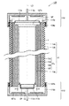
はじめに本実施の形態の発光装置の構成について説明する。図1および図2のそれぞれは、本発明の実施の形態1における発光装置の構成を概略的に示す外観図および断面図である。
Embodiments of the present invention will be described below.
(Embodiment 1)
First, the structure of the light emitting device of this embodiment will be described. 1 and 2 are an external view and a cross-sectional view schematically showing the configuration of the light-emitting device according to
図1および図2を参照して、本実施の形態の有機EL発光装置130は、円筒管1(基材)と、有機EL素子12と、封止部110と、電極112a、112bと、配線113a、113bと、乾燥剤127a、127bとを備えている。
With reference to FIG. 1 and FIG. 2, the organic EL light-emitting
円筒管1は、長さ方向(図中LD方向)に延びる空洞部を有する管である。すなわち円筒管1は管形状を有している。また円筒管1は透光性を有している。具体的には円筒管1は、たとえばソーダ石灰ガラスにより形成された、直径50mm、長さ540mm、厚さ1mmの管である。
The
有機EL素子12は、円筒管1の内面上に順に、保護層12aと、透明陽極層12b(第1電極層)と、有機物層OLと、陰極層12g(第2電極層)とを含んでいる。有機物層OLは、第1〜第4の層12c〜12fを有している。保護層12aと、透明陽極層12bと、有機物層OLと、陰極層12gとは、円筒管1の中心(図中LD方向)から同心円状に配置されている。
The
保護層12aは、アルカリ金属イオンの移動を防止する機能を有している。よって円筒管1の材質にソーダ石灰ガラスなどのアルカリ金属イオンを含む材質が用いられても、円筒管1から透明陽極層12bへアルカリ金属イオンが移動することが防止される。保護層12aは、たとえば酸化シリコン(SiO2)により形成された厚さ10nmの層である
。
The
透明陽極層12bは、透光性を有しており、かつ有機EL素子12の陽極としての機能を有している。透明陽極層12bは、導電性の酸化物層であり、たとえば酸化インジウム錫(ITO(Tin doped Indium Oxide))により形成された厚さ5μmの層である。
The
有機物層OLの第1の層12cは、たとえば下記の式(1)に示す有機材料(NPD)から形成された厚さ40nmの層である。
The
第2の層12dは、たとえば、下記の式(2)に示す有機材料(Znbox2)を主成分とし、かつ下記の式(3)に示すペリレン(C20H12)により1.5重量%のドーピングがなされた、厚さ7nmの層である。
The
第3の層12eは、たとえば、上記の式(2)に示す有機材料(Znbox2)を主成分とし、かつ下記の式(4)に示す有機材料(DCM1)により0.25重量%のドーピングがなされた、厚さ23nmの層である。
The
第4の層12fは、たとえば、上記の式(2)に示す有機材料(Znbox2)から形成された、厚さ30nmの層である。
The
なお上記の第1の層12cはホール輸送層としての機能を有し、第4の層12fは電子輸送層としての機能を有している。また第2の層12dおよび第3の層12eのそれぞれは、ドーパント色素としてペリレンおよびDCM1を含有することにより、発光層としての機能を有している。第2の層12dおよび第3の層12eのそれぞれにおいて青色およびオレンジ色の発光が生じ、これら2色の光が混合することで白色の光が得られる。
The
陰極層12gは、有機EL素子12の陰極としての機能を有している。陰極層12gは、金属層であり、たとえばアルミニウムにより形成された厚さ50nmの層である。
The
本実施の形態では、陰極層12gは円筒管1の内周側に配置され、透明陽極層12bは円筒管1の外周側に配置されている。また光を円筒管1の外部へ効率的に放出するために、陰極層12gは光を反射させる性質を有し、透明陽極層12bは光を透過させる性質を有している。このため、透明陽極層12bの材料と陰極層12gの材料とは異なっている。その結果、透明陽極層12bの材料と陰極層12gの材料とは、材料で決まる固有の電気抵抗値が異なっている。そこで、本実施の形態の陰極層12gにおいて、円筒管1の延びる方向に沿う単位長さ当たりの電気抵抗値が透明陽極層12bと同一になるように調節されている。言い換えると、電流経路に沿って透明陽極層12bおよび陰極層12gを切ったときの面の抵抗値が同一である。たとえば透明陽極層12bがITOで構成され、陰極層12gが金属で構成される場合には、陰極層12gの厚みは透明陽極層12bの厚みよりも薄くなる。
In the present embodiment, the
なお、透明陽極層12bの材料と陰極層12gの材料とは同一であってもよく、異なっていてもよい。
The material of the
なお、有機物層OL上の領域のうち円筒管1の長さ方向の両端側の領域は、陰極層12gが形成されていない。この陰極層12gが形成されていない領域は、ショート防止用スペースSPである。このショート防止用スペースSPが設けられていることにより、陰極層12gと透明陽極層12bとが有機EL素子12の端部において短絡することが防止されている。
In addition, the
封止部110は、封止部品110a、110b、およびOリング124a、124bを有している。封止部品110aおよび110bのそれぞれには、有機EL発光装置130の外部に向かって突出した電極112aおよび112bが配置されている。また封止部品110a、110bのそれぞれには、乾燥剤127a、127bが配置されている。封止部品110aおよび110bのそれぞれには、円筒管1の両端に、Oリング124a、124bにより着脱可能に固定されている。封止部110の材質は、たとえばガラスまたはアルミニウムである。各Oリング124a、124bは、エラストマーからなり、エラストマーの復元力により封止部品110aおよび110bのいずれかと、円筒管1とに密着されている。これにより封止部110は、不活性ガスIGが充填された円筒管1の内部を封止している。よって、有機EL素子12が形成された領域、すなわち有機物層OLと陰極層12gとを含む領域が、有機EL発光装置130の外部から気密に封止されている。なおOリング124a、124bによる封止をより確実にするため、封止部110にOリング124a、124bを締め付けるためのネジが取り付けられてもよい。
The sealing
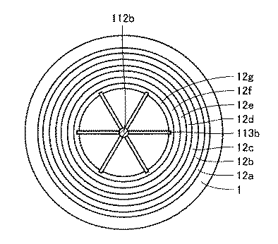
図3は、図2におけるIII−III線から見たときの模式図であり、透明陽極層12bと配線113aとの接続を概略的に示す。図3を参照して、透明陽極層12bの複数箇所と電極112a(第1外部電極)とは、電気的に接続されている。電極112aから透明陽極層12bの複数箇所までのそれぞれの距離が同じである。
FIG. 3 is a schematic diagram when viewed from the line III-III in FIG. 2 and schematically shows the connection between the
図4は、図2におけるIV−IV線から見たときの模式図であり、陰極層12gと配線113bとの接続を概略的に示す図である。図4を参照して、陰極層12gの複数箇所と電極112b(第2外部電極)とは、電気的に接続されている。電極112b(第2外部電極)から陰極層12gの複数箇所までのそれぞれの距離が同じである。
FIG. 4 is a schematic diagram when viewed from the line IV-IV in FIG. 2, and is a diagram schematically showing the connection between the
なお、上記「距離が同じ」とは、電極112aから透明陽極層12bの複数箇所までのそれぞれの電気抵抗値にばらつきがない程度であり、電極112bから陰極層12gの複数箇所までのそれぞれの電気抵抗値にばらつきがない程度である。
The above “same distance” means that there is no variation in the electric resistance values from the
また、電極112aは、透明陽極層12bの一方端部(円筒管1の外周側)で接続され、電極112bは、陰極層12gの他方端部(円筒管1の内周側)で接続されている。
The
本実施の形態では、配線113aの一端は透明陽極層12bに放射状に電気的に接続されており、配線113aの他端は電極112aに電気的に接続されている。また配線113bの一端は陰極層12gに放射状に電気的に接続されており、配線113bの他端は電極112bに電気的に接続されている。また電極112a、112bの各々は封止部品110a、110bの中心に貫通して形成されている。つまり、円筒管1の円周方向に対して配線113a、113bの長さをそれぞれ同じにすることができるので、配線113a、113bによる電気抵抗値の差を低減できる。この構成により、円筒管1の周方向において配線113a、113bの抵抗の差を低減することができる。このため、円筒管1の封止領域の外部に露出した電極112aと電極112bとの間に電圧を印加することで、透明陽極層12bと陰極層12gとの間の有機物層OLに均一な電位差が生じ、この電位差により有機物層OLに均一な電流が供給されて均一な発光が生じる。
In the present embodiment, one end of the
次に、本実施の形態の有機EL発光装置130を図5に示す等価回路図を用いて説明する。図5において、透明陽極層12bと陰極層12gとは抵抗で表し、有機EL素子12はダイオードと抵抗とで表している。その他の部分は薄膜ではないので電気抵抗が無視できるものとして実線で表している。
Next, the organic EL
図5に示すように、透明陽極層12bの材料と陰極層12gの材料とは、それぞれの機能に応じて異なっているので、透明陽極層12bの電気抵抗率(単位体積当たりの電気抵抗値)と陰極層12gの電気抵抗率(単位体積当たりの電気抵抗値)とはそれぞれ異なっている。しかし、透明陽極層12bおよび陰極層12gの少なくとも一方の膜厚を最適化することで、透明陽極層12bおよび陰極層12gの円筒管1の延びる方向に沿って対向する位置の単位長さ当たりの電気抵抗を同じにすることができる。このため、電極112aから透明陽極層12bに電流を供給し、他方の電極112bから陰極層12gに電流を取り出すと、円筒管1の長さ方向において円筒管1の長さに比例した同一の電圧降下がそれぞれ生じる。たとえば、10Vの直流電圧を印加した場合、透明陽極層12bの電気抵抗によって透明陽極層12bの中央では9Vになり、末端では8Vに電圧が降下する。陰極層12gの出口側の電圧を0Vとすると、陰極層12gの中央では1Vになり、末端では2Vの電圧が生じている。つまり、有機物層OLに印加される電位差は全ての位置で8Vと同一になる。このように電流を注入することで、円筒管1の長手方向において発光層(有機物層OL)に均一に電流を流すことができる。
As shown in FIG. 5, since the material of the
透明陽極層12bおよび陰極層12gにそれぞれ電圧を印加すると、電子と正孔とがそれぞれ注入される。注入された電子と正孔とが、電子輸送層としての第4の層12fおよびホール輸送層としての第1の層12cをそれぞれ通過し、発光層としての第2の層12dおよび第3の層12eで結合する。上述したように、本実施の形態では、有機物層OLに印加される電圧差は全ての位置で同一であるので、有機物層OLの膜厚が均一であれば、有機物層OLに流れる電流は円筒管1の延びる方向の全ての位置で同じになる。したがって、円筒管1の延びる方向において発光輝度のばらつきを抑制することができる。
When a voltage is applied to the
また、発光輝度のばらつきを抑制することができるので、複数の電極を分散して配置しなくても、大面積の有機物層OLを用いることができる。 In addition, since variation in light emission luminance can be suppressed, a large-area organic material layer OL can be used without disposing a plurality of electrodes in a dispersed manner.
さらに、発光輝度の低い領域の輝度を向上する必要がないので、この発光輝度の低い領域の輝度を向上するために電流量を増加する必要がない。このため、透明陽極層12bおよび陰極層12gの電気抵抗によって発生するジュール熱を低減することができる。したがって、有機EL発光装置130の発光効率を向上でき、かつ寿命を向上することができる。
Furthermore, since it is not necessary to improve the luminance of the low emission luminance area, it is not necessary to increase the amount of current in order to improve the luminance of the low emission luminance area. For this reason, Joule heat generated by the electrical resistance of the
なお本実施の形態においては有機物層OL、透明陽極層12bおよび陰極層12gの膜厚を均一にしているが、本発明はこれに限定されるものではない。たとえば、透明陽極層12bの膜厚を変化させたとしても、陰極層12gの膜厚を最適化することで、有機物層OLに印加される電位差が全ての場所で同じになっていればよい。
In the present embodiment, the organic layer OL, the
また本実施の形態においては透明陽極層12bは、陰極層12gの外周側に配置しているが、本発明はこれに限定されるものではない。透明陽極層12bが陰極層12gの内周側に配置されていてもよい。この場合、透明陽極層12bにおいて電極112aと接続される一方端部が円筒管1の内周側で、陰極層12gにおいて電極112bと接続される他方端部が円筒管1の外周側であってもよい。
In the present embodiment, the
また本実施の形態においては管(基材)として円筒管としているが、本発明はこれに限定されるものではない。たとえば管の断面形状が矩形であってもよい。 In this embodiment, a cylindrical tube is used as the tube (base material), but the present invention is not limited to this. For example, the cross-sectional shape of the tube may be rectangular.
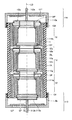
(変形例1)
図17は、実施の形態1の変形例1における有機EL発光装置の断面図である。図17を参照して、実施の形態1の変形例1における有機EL発光装置は、ショート防止用スペースSPを間に入れて3個の有機EL素子12(発光素子)を有している。一の有機EL素子12の陰極層12gは、隣接する他の有機EL素子12の透明陽極層12bと、接続配線114aで接続されている。つまり、複数の有機EL素子12は、相互に直列接続されている。なお、接続配線114aの代わりに陰極層12gを延長して、隣接する有機EL素子12の透明陽極層12bと接続してもよい。
(Modification 1)
FIG. 17 is a cross-sectional view of an organic EL light emitting device in
図18は、実施の形態1の変形例1における有機EL発光装置の等価回路図である。図18において、透明陽極層12bは抵抗で表し、有機EL素子12はダイオードと抵抗とで表している。その他の部分は薄膜ではないので電気抵抗が無視できるものとして実線で表している。
FIG. 18 is an equivalent circuit diagram of the organic EL light emitting device in
図18を参照して、電極112aから透明陽極層12bに電流を供給し、他方の電極112bから陰極層12gに電流を取り出すと、円筒管1の長さ方向において円筒管1の長さに比例した同一の電圧降下が各有機EL素子12においてそれぞれ生じる。このように電流を注入することで、円筒管1の長手方向において発光層(有機物層OL)に均一に電流を流すことができる。
Referring to FIG. 18, when a current is supplied from the
図19は、実施の形態1の変形例1における有機EL発光装置の概念図である。図19(A)を参照して、円筒管1の延びる方向の透明陽極層12bの電気抵抗が0.5Ωで、5Vの電圧で、かつ5Aの電流で発光する有機EL素子12は、透明陽極層12bからおよそ12.5W発熱する。図19(B)を参照して、この有機EL素子12を5分割して直列に接続すると、1個あたりの円筒管1の延びる方向の透明陽極層12bの電気抵抗は0.1Ωになる。分割した有機EL素子12の面積は1/5になるので、発光に必要な電流も1/5の1Aになるが、円筒管1の内側の方向、有機物層OLから陰極層12gへの電気抵抗は5倍になる。ゆえに、分割した有機EL素子12の1つは5Vの電圧で、かつ1Aの電流で発光し、直列に5個接続した場合、25Vの電圧で、かつ1Aの電流で発光する。このとき、個々の透明陽極層12bはおよそ0.1W発熱し、5個の合計でも0.5Wの発熱に抑制できる。すなわち、有機EL素子12を5分割することにより発熱量を1/25に減らすことができる。
FIG. 19 is a conceptual diagram of an organic EL light emitting device in
(変形例2)
図20は、実施の形態1の変形例2における有機EL発光装置の断面図である。図20を参照して、実施の形態1の変形例2における有機EL素子12は、円筒管1の外周から内周に向けて、透明陽極層12b(第1電極層)、有機物層OL(有機物層)、陰極層12g(第2電極層)、透明陽極層12b(第3電極層)、有機物層OL(第2有機物層)、および陰極層12g(第4電極層)の順番に形成されている。透明陽極層12b(第1電極層)、有機物層OL(有機物層)および陰極層12g(第2電極層)で第1発光素子(第1有機EL素子)を形成し、透明陽極層12b(第3電極層)、有機物層OL(第2有機物層)および陰極層12g(第4電極層)で第2発光素子(第2有機EL素子)を形成している。つまり、有機EL素子12は、第1発光素子と第2発光素子とを含んでいる。透明陽極層12b(第1電極層)の電気抵抗値と陰極層12g(第2電極層)の電気抵抗値とは同じであり、かつ、透明陽極層12b(第3電極層)の電気抵抗値と陰極層12g(第4電極層)の電気抵抗値とは同じである。
(Modification 2)
FIG. 20 is a cross-sectional view of an organic EL light emitting device in
有機物層OLと透明陽極層12bとの間(中間部)の陰極層12gは、透明な材料が使用されている。各有機EL素子12は、配線113a、113bと、接続配線114a、114bとで接続されている。電極112a、112bに交流を印加すると、プラスとマイナスとの極性が交互に入れ替わる。電極112aがプラスで電極112bがマイナスの場合、外側の有機物層OLが順方向電圧となって電流が流れ、発光する。内側の有機物層OLは逆方向電圧となっているので電流が流れない。次に極性が反転し、電極112aがマイナスで電極112bがプラスの場合、内側の有機物層OLが順方向電圧となって電流が流れ、発光する。外側の有機物層OLは逆方向電圧となっているので電流が流れない。
A transparent material is used for the
図21および図22は、実施の形態1の変形例2における有機EL発光装置の等価回路図である。図21は、電極112aがプラスで電極112bがマイナスの場合の等価回路図であり、図22は、電極112aがマイナスで電極112bがプラスの場合の等価回路図である。図21および図22において、透明陽極層12bは抵抗で表し、有機EL素子12はダイオードと抵抗とで表している。その他の部分は薄膜ではないので電気抵抗が無視できるものとして実線で表している。
21 and 22 are equivalent circuit diagrams of the organic EL light emitting device in
図21および図22を参照して、電極112a、112bに交流を供給すると、円筒管1の長さ方向において円筒管1の長さに比例した同一の電圧降下がそれぞれ生じる。このように交流の場合であっても、円筒管1の長手方向において発光層(有機物層OL)に均一に電流を流すことができる。
Referring to FIGS. 21 and 22, when alternating current is supplied to
(変形例3)
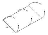
図23は、本発明の実施の形態1の変形例3の有機EL発光装置の構成の断面図である。実施の形態1の変形例3の有機EL発光装置は、円筒管1の内側で、かつ透明陽極層12bの外側に円筒管1の延びる方向に沿って形成され、曲げることが可能な透光性を有する基板をさらに備えている。図24および図25は、実施の形態1の変形例3の基板を示す模式図である。図23および図24を参照して、変形例3の基板は、たとえばフレキシブル基板115を用いている。
(Modification 3)
FIG. 23 is a cross-sectional view of the configuration of the organic EL light emitting device of Modification 3 of
変形例3では、円筒管1の内面上に順に、フレキシブル基板115と、透明陽極層12bと、有機物層OLと、陰極層12gとが形成されている。変形例3では、円筒管1の内面上にフレキシブル基板115が形成されているので、保護層12aは形成されていない。なお、フレキシブル基板115と円筒管1との間に保護層12aが形成されていてもよい。
In Modification 3, a
変形例3の有機EL発光装置を製造する場合には、たとえば以下の方法により行なうことができる。まず、図24を参照して、フレキシブル基板115を準備し、矢印の方向に曲げる。これにより、図25に示すように円筒形状のフレキシブル基板115を形成できる。図25に示すフレキシブル基板115を、円筒管1の内部に図26に示す矢印の方向に沿って挿入する。なお、図26は、実施の形態1の変形例3の有機EL発光装置の製造過程を示す模式図である。その後、有機EL素子12などを形成することで、図23に示す変形例3の有機EL発光装置を製造することができる。
When manufacturing the organic EL light-emitting device of the modification 3, it can carry out by the following methods, for example. First, referring to FIG. 24, a
ここで、変形例3の有機EL発光装置の製造方法は、上記方法に限定されず、図24に示すフレキシブル基板115の上に有機EL素子12を形成した後、図25に示すように、円筒形状にして、図26に示す円筒管1に挿入してもよい。
Here, the manufacturing method of the organic EL light emitting device of Modification 3 is not limited to the above method, and after forming the
(変形例4)
図27は、本発明の実施の形態1の変形例4の有機EL発光装置の構成の断面図である。図28および図29は、実施の形態1の変形例4のフレキシブル基板および補助電極を示す模式図である。図27〜図29を参照して、実施の形態1の変形例4の有機EL発光装置は、変形例3のフレキシブル基板115、透明陽極層12b、有機物層OLおよび陰極層12gが複数(図27では2層)積層され、陰極層12gに接触している帯状の補助電極114をさらに備えている。補助電極114は、積層されたフレキシブル基板115の内部のコンタクトをとるために設けられている。
(Modification 4)
FIG. 27 is a cross-sectional view of the configuration of the organic EL light emitting device of Modification 4 of
変形例4は、円筒管1の内面上に順に、フレキシブル基板115と、透明陽極層12bと、有機物層OLと、陰極層12gと、フレキシブル基板115と、透明陽極層12bと、有機物層OLと、陰極層12gとが形成されている。つまり、フレキシブル基板115と透明陽極層12bと有機物層OLと陰極層12gとを有する積層体を複数含み、複数の積層体は筒状に重なるように巻かれている。有機物層OLとフレキシブル基板115との間に位置している陰極層12gは透光性を有していることが好ましく、酸化インジウム錫などを用いることができる。
In Modification 4, the
変形例4では、補助電極114は、配線113a、113bと、複数の陰極層12gとをそれぞれ接続している。補助電極114は、陰極層12gの代わりに透明陽極層12bと接続されていてもよい。
In the fourth modification, the
変形例4の有機EL発光装置を製造する場合には、たとえば以下の方法により行なうことができる。まず、図28を参照して、フレキシブル基板115と、フレキシブル基板115の長さ方向の両端側の領域に形成された補助電極114と、フレキシブル基板115上に形成された有機EL素子12とを有する積層物を準備する。その後、この積層物を図28に示す矢印の方向に曲げる。これにより、積層物を図29に示すように円筒形状に形成できる。図29に示す円筒形状のフレキシブル基板115などを、円筒管1の内部に図26に示す矢印の方向に沿って挿入することで、図27に示す変形例4の有機EL発光装置を製造することができる。
When manufacturing the organic EL light-emitting device of the modification 4, it can carry out, for example with the following method. First, referring to FIG. 28, it has a
(変形例5)
図30および図31は、本発明の実施の形態1の変形例5の金属電極を示す模式図である。図30および図31に示すように、変形例5の有機EL発光装置は、第1電極層である透明陽極層12bに接続され、かつ透明陽極層12bの電気抵抗を減らすための直線または金網状の金属電極12iをさらに備えている。金属電極12iは、図30に示すように直線、つまりストライプ状であってもよく、図31に示すように金網状、つまりメッシュ状であってもよい。また、図30および図31では、透明陽極層12bの外周に金属電極12iが形成されているが、内周に形成されていてもよい。
(Modification 5)
30 and 31 are schematic views showing a metal electrode of Modification 5 of
透明陽極層12bは透光性を有しているので、通常の金属に比べて電気抵抗が大きい。このため、透明陽極層12bの外側または内側に直線または金網状の金属電極12iを設けることにより、電気抵抗を低減することができる。
Since the
(実施の形態2)
はじめに、図6を参照して、本実施の形態の有機EL発光装置の構成について説明する。図6は本発明の実施の形態2における有機EL発光装置の概略的な断面図である。図6を参照して、本実施の形態の有機EL発光装置130では、実施の形態1における有機物層OLと陰極層12gとの間に位置し、かつ円筒管1の延びる方向に沿って配置された引き出し電極112cをさらに備えている。
(Embodiment 2)
First, the configuration of the organic EL light emitting device of the present embodiment will be described with reference to FIG. FIG. 6 is a schematic cross-sectional view of an organic EL light-emitting device according to
図6を参照して、電極112bは、円筒管1の延びる方向に沿って延在し、有機物層OLと対向している。この電極112bの円筒管1の内部であって、かつ有機物層OLと対向する領域上に陰極層12gが形成されている。この陰極層12gは、有機物層OLから空間的に離れた位置に設けられている。陰極層12gが形成された領域の電極112bと
、陰極層12gとで陰極12hを構成している。この陰極層12gは、たとえばカーボンナノチューブ、シリコンナノ結晶層などの電子放出源を用いることができる。
Referring to FIG. 6, the
有機物層OLと陰極12hとの間の空間は、真空VSである。本実施の形態では、円筒管1の内部は、真空VSに保たれている。
A space between the organic material layer OL and the
引き出し電極112cは、陰極層12gと有機物層OLとの間に配置されている。この引き出し電極112cは、陰極層12gから放出された電子を有機物層OLに注入する際に、電界や磁界により制御することにより、整流、発振、変調、検波、増幅などの作用を行なうことができるように構成されている。このような引き出し電極112cとして、たとえばメッシュ状の金属部材を用いることができる。
The
次に、本実施の形態の有機EL発光装置130を図7に示す等価回路図で説明する。図7において、透明陽極層12bは抵抗で表し、有機EL素子12はダイオードと抵抗とで表している。その他の部分は薄膜ではないので電気抵抗が無視できるものとして実線で表している。
Next, the organic EL
図7を参照して、引き出し電極112cに電圧を印加すると、陰極12hの表面に形成した陰極層12gから電子eが放出される。放出された電子eは引き出し電極112cの間を通過し、有機物層OLに注入される。このため、有機EL素子12に電流が注入される。
Referring to FIG. 7, when a voltage is applied to
なお、引き出し電極112cに高電圧を印加して陰極12hから電子eが放出されるので、電子eの放出は透明陽極層12bの抵抗に影響されない。
Note that, since a high voltage is applied to the
本実施の形態における有機EL発光装置130によれば、有機物層OLと陰極層12gとの間に位置し、かつ円筒管1の延びる方向に沿って配置された引き出し電極112cをさらに備えている。このため、陰極層12gから引き出し電極112cを介して有機物層OLまでを電子eが直進することにより、有機物層OLに均一な電流を注入することができる。したがって、有機EL発光装置130の発光輝度のばらつきをより抑制することができる。
According to the organic EL
また本実施の形態においては、電子eを効率よく有機物層OLに注入することができるので、たとえば電流密度が0.14mA/cm2以上で、発光効率が138cd/A以上の高い電流効率で発光させることができる。 In the present embodiment, since electrons e can be efficiently injected into the organic layer OL, for example, light emission is performed with a high current efficiency such as a current density of 0.14 mA / cm 2 or more and a light emission efficiency of 138 cd / A or more. Can be made.
さらに、実施の形態1と異なり、本実施の形態では陰極12hと有機物層OLとの間に真空VSの領域が形成されている。このため、有機物層OLに生じる点欠陥によってショートすることを抑制することができる。
Furthermore, unlike
上記の有機EL発光装置130において好ましくは、陰極層12gにカーボンナノチューブを使用する。カーボンナノチューブは印加電圧が閾値電圧に達すると、セルフエミッション現象によって、自動的な電子放出が全体で生じる。このため、より均一な電子注入が得られるので、発光輝度のばらつきをより抑制することができる。
In the organic EL
また有機EL発光装置130において好ましくは、陰極層12gにシリコンナノ結晶層を使用する。シリコンナノ結晶層は印加電圧が閾値電圧に達すると、弾道電子放出現象によって、自動的な電子放出が全体で生じる。このため、より均一な電子注入が得られるので、発光輝度のばらつきをより抑制することができる。
In the organic EL
なお、上記以外の構成については、上述した実施の形態1の構成とほぼ同じであるため、同一または対応する要素について同一の符号を付し、その説明を繰り返さない。 Since the configuration other than the above is substantially the same as the configuration of the first embodiment described above, the same or corresponding elements are denoted by the same reference numerals, and description thereof is not repeated.
(実施の形態3)
はじめに本実施の形態の有機EL照明装置の構成について説明する。図8は、本発明の実施の形態3における有機EL照明装置の構成を概略的に示す側面図であり、図9は上面図である。本実施の形態の有機EL照明装置は、複数の有機EL発光装置130と、この有機EL発光装置130を接続する連結器131とを備えている。
(Embodiment 3)
First, the configuration of the organic EL lighting device according to the present embodiment will be described. FIG. 8 is a side view schematically showing the configuration of the organic EL lighting device according to Embodiment 3 of the present invention, and FIG. 9 is a top view. The organic EL lighting device of the present embodiment includes a plurality of organic EL
図8および図9を参照して、本実施の形態の有機EL照明装置は、4本の円筒型有機EL発光装置130の両端にある電極112a、112b(図2および図6参照)を連結器131で固定している。両端に配置された連結器131は反射鏡132で結合されていて、個々の有機EL発光装置130は容易に取り外し可能な構造を有している。
8 and 9, in the organic EL lighting device of the present embodiment,
なお電極112a、112bにはプラスおよびマイナスの極性を有しているので、電極112a、112bを異なった形状にして、それぞれを連結器131と結合させている。
Since the
図10および図11は、本発明の実施の形態3における有機EL照明装置の等価回路図である。図10および図11を参照して、個々の有機EL発光装置130はダイオードと抵抗で表している。その他の部分は金属配線なので電気抵抗が無視できるものとして実線で表している。
10 and 11 are equivalent circuit diagrams of the organic EL lighting device according to Embodiment 3 of the present invention. With reference to FIGS. 10 and 11, each organic EL
有機EL照明装置は、4本の有機EL発光装置130は連結器131の内部で、図10に示すように直列接続、または図11に示すように並列接続されている。
In the organic EL lighting device, four organic EL
(変形例1)
図12は実施の形態3の変形例1における有機EL照明装置の構成を概略的に示す外観図である。図12に示すように、平面形状が四角形になるように、4本の有機EL発光装置130を4個の連結器131を用いて接続している。
(Modification 1)
FIG. 12 is an external view schematically showing a configuration of an organic EL lighting device in
(変形例2)
図13は、実施の形態3の変形例2における有機EL照明装置の構成を概略的に示す外観図である。図13に示すように、平面形状が六角形になるように、6本の有機EL発光装置130を6個の連結器131を用いて接続している。
(Modification 2)
FIG. 13 is an external view schematically showing a configuration of an organic EL lighting device in
(変形例3)
図14は、実施の形態3の変形例3における有機EL照明装置の構成を概略的に示す外観図である。図14に示すように、平面形状が八角形になるように、8本の有機EL発光装置130を8個の連結器131を用いて接続している。
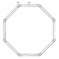
(Modification 3)
FIG. 14 is an external view schematically showing a configuration of an organic EL lighting device in Modification 3 of Embodiment 3. As shown in FIG. 14, eight organic EL
(変形例4)
図15は、実施の形態3の変形例4における有機EL照明装置の構成を概略的に示す外観図である。図15に示すように、直線をなすように、3本の有機EL発光装置130を2個の連結器131を用いて接続している。
(Modification 4)
FIG. 15 is an external view schematically showing a configuration of an organic EL lighting device in Modification 4 of Embodiment 3. As shown in FIG. 15, three organic EL
(変形例5)
図16は、実施の形態3の変形例5における有機EL照明装置の構成を概略的に示す外観図である。図16に示すように、本変形例における連結器131は、6本の有機EL発光装置130を連結している。このため、この連結器131は、6本の有機EL発光装置130を放射状に接続している。
(Modification 5)
FIG. 16 is an external view schematically showing a configuration of an organic EL lighting device in Modification 5 of Embodiment 3. As shown in FIG. 16, the
本実施の形態およびその変形例の有機EL照明装置によれば、複数の有機EL発光装置130と、この複数の有機EL発光装置130を接続する連結器131を備えている。連結器131によって、複数の有機EL発光装置130を直列または並列に接続して1組の有機EL照明装置としている。このため、任意の形状の有機EL照明装置を実現することができる。
According to the organic EL lighting device of the present embodiment and the modification thereof, the plurality of organic EL
また、上記有機EL照明装置において好ましくは、連結器131は、有機EL発光装置130と着脱可能である。このため、複数の有機EL発光装置130の一部を交換するなど必要に応じて有機EL発光装置130を取り外すことができる。したがって、利便性を向上することができる。
In the organic EL lighting device, the
今回開示された実施の形態はすべての点で例示であって制限的なものではないと考えられるべきである。本発明の範囲は上記した説明ではなくて特許請求の範囲によって示され、特許請求の範囲と均等の意味および範囲内でのすべての変更が含まれることが意図される。 The embodiment disclosed this time should be considered as illustrative in all points and not restrictive. The scope of the present invention is defined by the terms of the claims, rather than the description above, and is intended to include any modifications within the scope and meaning equivalent to the terms of the claims.
本発明は、発光輝度のばらつきを抑制することができる有機EL発光装置を実現できるので、大面積で均一に発光することが要求される有機EL発光装置、特に有機EL照明装置に適用され得る。 The present invention can realize an organic EL light emitting device capable of suppressing variations in light emission luminance, and thus can be applied to an organic EL light emitting device that is required to emit light uniformly over a large area, particularly an organic EL lighting device.
1 円筒管、12 有機EL素子、12a 保護層、12b 透明陽極層、12c 第1の層、12d 第2の層、12e 第3の層、12f 第4の層、12g 陰極層、12h 陰極、12i 金属電極、110 封止部、110a,110b 封止部品、112a,112b 電極、112c 引き出し電極、113a,113b 配線、114 補助電極、114a,114b 接続配線、115 フレキシブル基板、124a,124b Oリング、127a,127b 乾燥剤、130 有機EL発光装置、131 連結器、132 反射鏡、OL 有機物層、SP ショート防止用スペース、IG 不活性ガス、VS 真空、e 電子。
DESCRIPTION OF
Claims (1)
前記管の内側に前記管の延びる方向に沿って形成され、透光性を有する第1電極層と、
前記第1電極層の内側に前記管の延びる方向に沿って形成され、電圧が印加されることにより発光する有機物層と、
前記有機物層の内側に前記管の延びる方向に沿って形成された第2電極層とを備え、
前記第1電極層および前記第2電極層のいずれか一方が陽極で、他方が陰極であり、
前記第1電極層の電気抵抗値と前記第2電極層の電気抵抗値とは同じであり、
前記第1電極層と電気的に接続された第1外部電極と、
前記第2電極層と電気的に接続された第2外部電極と、
前記第1電極層の複数箇所と前記第1外部電極とを接続する複数の第1配線と、
前記第2電極層の複数箇所と前記第2外部電極とを接続する複数の第2配線とをさらに備え、
複数の前記第1配線は、前記第1外部電極を中心として前記第1電極層の前記複数箇所へ放射状にそれぞれ接続され、
複数の前記第2配線は、前記第2外部電極を中心として前記第2電極層の前記複数箇所へ放射状にそれぞれ接続され、
前記第1外部電極から前記第1電極層の前記複数箇所までのそれぞれの距離が同じであり、
前記第2外部電極から前記第2電極層の前記複数箇所までのそれぞれの距離が同じである、有機EL発光装置。 A translucent tube;
A first electrode layer formed inside the tube along the direction in which the tube extends and having translucency;
An organic material layer that is formed inside the first electrode layer along a direction in which the tube extends and emits light when a voltage is applied;
A second electrode layer formed along the direction in which the tube extends inside the organic layer,
Either one of the first electrode layer and the second electrode layer is an anode, the other is a cathode,
Ri same Der the electrical resistance of the second electrode layer and the electric resistance value of the first electrode layer,
A first external electrode electrically connected to the first electrode layer;
A second external electrode electrically connected to the second electrode layer;
A plurality of first wirings connecting the plurality of locations of the first electrode layer and the first external electrode;
A plurality of second wires connecting the plurality of locations of the second electrode layer and the second external electrode;
The plurality of first wirings are respectively connected radially to the plurality of locations of the first electrode layer around the first external electrode,
The plurality of second wirings are respectively connected radially to the plurality of locations of the second electrode layer around the second external electrode,
Each distance from the first external electrode to the plurality of locations of the first electrode layer is the same,
The organic EL light emitting device, wherein each distance from the second external electrode to the plurality of locations of the second electrode layer is the same .
Priority Applications (1)
| Application Number | Priority Date | Filing Date | Title |
|---|---|---|---|
| JP2009090083A JP4533963B2 (en) | 2008-05-01 | 2009-04-02 | Organic EL light emitting device |
Applications Claiming Priority (2)
| Application Number | Priority Date | Filing Date | Title |
|---|---|---|---|
| JP2008119863 | 2008-05-01 | ||
| JP2009090083A JP4533963B2 (en) | 2008-05-01 | 2009-04-02 | Organic EL light emitting device |
Publications (2)
| Publication Number | Publication Date |
|---|---|
| JP2009289742A JP2009289742A (en) | 2009-12-10 |
| JP4533963B2 true JP4533963B2 (en) | 2010-09-01 |
Family
ID=41458732
Family Applications (1)
| Application Number | Title | Priority Date | Filing Date |
|---|---|---|---|
| JP2009090083A Expired - Fee Related JP4533963B2 (en) | 2008-05-01 | 2009-04-02 | Organic EL light emitting device |
Country Status (1)
| Country | Link |
|---|---|
| JP (1) | JP4533963B2 (en) |
Cited By (1)
| Publication number | Priority date | Publication date | Assignee | Title |
|---|---|---|---|---|
| CN102544311A (en) * | 2010-11-19 | 2012-07-04 | 株式会社半导体能源研究所 | Lighting device |
Families Citing this family (6)
| Publication number | Priority date | Publication date | Assignee | Title |
|---|---|---|---|---|
| US8525407B2 (en) | 2009-06-24 | 2013-09-03 | Semiconductor Energy Laboratory Co., Ltd. | Light source and device having the same |
| KR101642117B1 (en) * | 2010-04-22 | 2016-07-25 | 삼성디스플레이 주식회사 | Organic light emitting device |
| US9781783B2 (en) | 2011-04-15 | 2017-10-03 | Semiconductor Energy Laboratory Co., Ltd. | Light-emitting device, display device, light-emitting system, and display system |
| WO2013125436A1 (en) * | 2012-02-20 | 2013-08-29 | 株式会社カネカ | Organic el device and method for manufacturing organic el device |
| GB2505499B (en) * | 2012-09-03 | 2017-03-08 | Dst Innovations Ltd | Electroluminescent displays and lighting |
| DE102013107116B4 (en) * | 2013-07-05 | 2022-05-25 | Pictiva Displays International Limited | Organic light-emitting diode and method for operating an organic light-emitting diode |
Citations (10)
| Publication number | Priority date | Publication date | Assignee | Title |
|---|---|---|---|---|
| JP2002325162A (en) * | 2001-02-22 | 2002-11-08 | Matsushita Electric Ind Co Ltd | Light source for image reading apparatus and image reading apparatus |
| JP2003142252A (en) * | 2001-11-01 | 2003-05-16 | Harison Toshiba Lighting Corp | Tubular light emitting device |
| JP2004134359A (en) * | 2002-08-05 | 2004-04-30 | General Electric Co <Ge> | Serially connected oled structure and fabrication method |
| JP2005108516A (en) * | 2003-09-29 | 2005-04-21 | Seiko Epson Corp | Organic el device and power supplying device |
| JP2007073403A (en) * | 2005-09-08 | 2007-03-22 | Toppan Printing Co Ltd | Surface light emitting device |
| JP2007173213A (en) * | 2005-12-22 | 2007-07-05 | Lg Electron Inc | Organic electroluminescent element with scan line having uniform resistance value |
| JP2007311159A (en) * | 2006-05-18 | 2007-11-29 | Toyota Industries Corp | Organic electroluminescent element |
| JP2007536708A (en) * | 2004-05-04 | 2007-12-13 | イーストマン コダック カンパニー | Tile flat panel lighting system |
| JP2008117742A (en) * | 2006-11-07 | 2008-05-22 | Micro System:Kk | Cylindrical organic el illuminator |
| JP2009076269A (en) * | 2007-09-19 | 2009-04-09 | Panasonic Electric Works Co Ltd | Light source device |
Family Cites Families (2)
| Publication number | Priority date | Publication date | Assignee | Title |
|---|---|---|---|---|
| JP3137494B2 (en) * | 1993-04-22 | 2001-02-19 | 三菱電機株式会社 | Electroluminescent device and display device using the same |
| KR100805038B1 (en) * | 2006-05-04 | 2008-02-20 | 주식회사 엘지화학 | Organic Light Emitting Diode And Method For Preparing Thereof |
-
2009
- 2009-04-02 JP JP2009090083A patent/JP4533963B2/en not_active Expired - Fee Related
Patent Citations (10)
| Publication number | Priority date | Publication date | Assignee | Title |
|---|---|---|---|---|
| JP2002325162A (en) * | 2001-02-22 | 2002-11-08 | Matsushita Electric Ind Co Ltd | Light source for image reading apparatus and image reading apparatus |
| JP2003142252A (en) * | 2001-11-01 | 2003-05-16 | Harison Toshiba Lighting Corp | Tubular light emitting device |
| JP2004134359A (en) * | 2002-08-05 | 2004-04-30 | General Electric Co <Ge> | Serially connected oled structure and fabrication method |
| JP2005108516A (en) * | 2003-09-29 | 2005-04-21 | Seiko Epson Corp | Organic el device and power supplying device |
| JP2007536708A (en) * | 2004-05-04 | 2007-12-13 | イーストマン コダック カンパニー | Tile flat panel lighting system |
| JP2007073403A (en) * | 2005-09-08 | 2007-03-22 | Toppan Printing Co Ltd | Surface light emitting device |
| JP2007173213A (en) * | 2005-12-22 | 2007-07-05 | Lg Electron Inc | Organic electroluminescent element with scan line having uniform resistance value |
| JP2007311159A (en) * | 2006-05-18 | 2007-11-29 | Toyota Industries Corp | Organic electroluminescent element |
| JP2008117742A (en) * | 2006-11-07 | 2008-05-22 | Micro System:Kk | Cylindrical organic el illuminator |
| JP2009076269A (en) * | 2007-09-19 | 2009-04-09 | Panasonic Electric Works Co Ltd | Light source device |
Cited By (1)
| Publication number | Priority date | Publication date | Assignee | Title |
|---|---|---|---|---|
| CN102544311A (en) * | 2010-11-19 | 2012-07-04 | 株式会社半导体能源研究所 | Lighting device |
Also Published As
| Publication number | Publication date |
|---|---|
| JP2009289742A (en) | 2009-12-10 |
Similar Documents
| Publication | Publication Date | Title |
|---|---|---|
| JP4533963B2 (en) | Organic EL light emitting device | |
| JP6108664B2 (en) | Organic EL device | |
| EP2985803B1 (en) | Organic light-emitting device and method of manufacturing same | |
| US20060197077A1 (en) | Metal complex compound and organic electroluminescent device using same | |
| KR101512265B1 (en) | Organic light emitting device | |
| EP2960961B1 (en) | Organic light emitting element | |
| JP2007258690A (en) | Light-emitting element unit using ac voltage | |
| US9219101B2 (en) | Organic EL device and method for manufacturing organic EL device | |
| TW201318471A (en) | Organic electroluminescent device with space charge/voltage instability stabilization drive | |
| JP4950850B2 (en) | Organic electroluminescence device | |
| JP5717373B2 (en) | Organic light emitting device | |
| KR101399779B1 (en) | Organic lihgt emitting devices and light emitting apparatus comprising the same | |
| JP5102570B2 (en) | Light source device | |
| JP2012160702A (en) | Optical semiconductor device | |
| JP3743005B2 (en) | Organic EL panel | |
| JP5058521B2 (en) | Flexible light emitter and flexible substrate used therefor | |
| KR100965243B1 (en) | Light emitting diode for ac operation | |
| JP4932068B1 (en) | Optical semiconductor device | |
| JP2009164070A (en) | Organic el element and organic el light-emitting device using the same | |
| KR101325531B1 (en) | Oled module and manufacturing method thereof | |
| KR101512218B1 (en) | Organic light emitting device | |
| JP5556594B2 (en) | Lighting device | |
| JP5741203B2 (en) | Manufacturing method of organic EL element | |
| KR101803011B1 (en) | Light-emitting device | |
| JP2012049062A (en) | Lighting apparatus |
Legal Events
| Date | Code | Title | Description |
|---|---|---|---|
| A621 | Written request for application examination |
Free format text: JAPANESE INTERMEDIATE CODE: A621 Effective date: 20091130 |
|
| A871 | Explanation of circumstances concerning accelerated examination |
Free format text: JAPANESE INTERMEDIATE CODE: A871 Effective date: 20091130 |
|
| A975 | Report on accelerated examination |
Free format text: JAPANESE INTERMEDIATE CODE: A971005 Effective date: 20091218 |
|
| A131 | Notification of reasons for refusal |
Free format text: JAPANESE INTERMEDIATE CODE: A131 Effective date: 20100302 |
|
| A521 | Request for written amendment filed |
Free format text: JAPANESE INTERMEDIATE CODE: A523 Effective date: 20100428 |
|
| TRDD | Decision of grant or rejection written | ||
| A01 | Written decision to grant a patent or to grant a registration (utility model) |
Free format text: JAPANESE INTERMEDIATE CODE: A01 Effective date: 20100525 |
|
| A01 | Written decision to grant a patent or to grant a registration (utility model) |
Free format text: JAPANESE INTERMEDIATE CODE: A01 |
|
| A61 | First payment of annual fees (during grant procedure) |
Free format text: JAPANESE INTERMEDIATE CODE: A61 Effective date: 20100614 |
|
| R150 | Certificate of patent or registration of utility model |
Free format text: JAPANESE INTERMEDIATE CODE: R150 |
|
| FPAY | Renewal fee payment (event date is renewal date of database) |
Free format text: PAYMENT UNTIL: 20130618 Year of fee payment: 3 |
|
| LAPS | Cancellation because of no payment of annual fees |