JP5571289B2 - Exposure mask and pattern forming method - Google Patents
Exposure mask and pattern forming method Download PDFInfo
- Publication number
- JP5571289B2 JP5571289B2 JP2008028381A JP2008028381A JP5571289B2 JP 5571289 B2 JP5571289 B2 JP 5571289B2 JP 2008028381 A JP2008028381 A JP 2008028381A JP 2008028381 A JP2008028381 A JP 2008028381A JP 5571289 B2 JP5571289 B2 JP 5571289B2
- Authority
- JP
- Japan
- Prior art keywords
- pattern
- mask
- phase shift
- exposure
- light
- Prior art date
- Legal status (The legal status is an assumption and is not a legal conclusion. Google has not performed a legal analysis and makes no representation as to the accuracy of the status listed.)
- Expired - Fee Related
Links
Images


Classifications
-
- G—PHYSICS
- G03—PHOTOGRAPHY; CINEMATOGRAPHY; ANALOGOUS TECHNIQUES USING WAVES OTHER THAN OPTICAL WAVES; ELECTROGRAPHY; HOLOGRAPHY
- G03F—PHOTOMECHANICAL PRODUCTION OF TEXTURED OR PATTERNED SURFACES, e.g. FOR PRINTING, FOR PROCESSING OF SEMICONDUCTOR DEVICES; MATERIALS THEREFOR; ORIGINALS THEREFOR; APPARATUS SPECIALLY ADAPTED THEREFOR
- G03F1/00—Originals for photomechanical production of textured or patterned surfaces, e.g., masks, photo-masks, reticles; Mask blanks or pellicles therefor; Containers specially adapted therefor; Preparation thereof
- G03F1/26—Phase shift masks [PSM]; PSM blanks; Preparation thereof
- G03F1/32—Attenuating PSM [att-PSM], e.g. halftone PSM or PSM having semi-transparent phase shift portion; Preparation thereof
-
- G—PHYSICS
- G03—PHOTOGRAPHY; CINEMATOGRAPHY; ANALOGOUS TECHNIQUES USING WAVES OTHER THAN OPTICAL WAVES; ELECTROGRAPHY; HOLOGRAPHY
- G03F—PHOTOMECHANICAL PRODUCTION OF TEXTURED OR PATTERNED SURFACES, e.g. FOR PRINTING, FOR PROCESSING OF SEMICONDUCTOR DEVICES; MATERIALS THEREFOR; ORIGINALS THEREFOR; APPARATUS SPECIALLY ADAPTED THEREFOR
- G03F7/00—Photomechanical, e.g. photolithographic, production of textured or patterned surfaces, e.g. printing surfaces; Materials therefor, e.g. comprising photoresists; Apparatus specially adapted therefor
- G03F7/70—Microphotolithographic exposure; Apparatus therefor
- G03F7/70058—Mask illumination systems
- G03F7/70125—Use of illumination settings tailored to particular mask patterns
-
- G—PHYSICS
- G03—PHOTOGRAPHY; CINEMATOGRAPHY; ANALOGOUS TECHNIQUES USING WAVES OTHER THAN OPTICAL WAVES; ELECTROGRAPHY; HOLOGRAPHY
- G03F—PHOTOMECHANICAL PRODUCTION OF TEXTURED OR PATTERNED SURFACES, e.g. FOR PRINTING, FOR PROCESSING OF SEMICONDUCTOR DEVICES; MATERIALS THEREFOR; ORIGINALS THEREFOR; APPARATUS SPECIALLY ADAPTED THEREFOR
- G03F7/00—Photomechanical, e.g. photolithographic, production of textured or patterned surfaces, e.g. printing surfaces; Materials therefor, e.g. comprising photoresists; Apparatus specially adapted therefor
- G03F7/70—Microphotolithographic exposure; Apparatus therefor
- G03F7/70483—Information management; Active and passive control; Testing; Wafer monitoring, e.g. pattern monitoring
- G03F7/7055—Exposure light control in all parts of the microlithographic apparatus, e.g. pulse length control or light interruption
- G03F7/70566—Polarisation control
Landscapes
- Physics & Mathematics (AREA)
- General Physics & Mathematics (AREA)
- Exposure And Positioning Against Photoresist Photosensitive Materials (AREA)
- Preparing Plates And Mask In Photomechanical Process (AREA)
Description
本発明は、露光用マスク及びパターン形成方法に関し、更に詳しくは、半導体ウエハ上に露光用マスクに対応するパターンを形成するパターン形成方法、及びこの方法に用いられる露光用マスクに関する。 The present invention relates to an exposure mask and a pattern formation method, and more particularly to a pattern formation method for forming a pattern corresponding to an exposure mask on a semiconductor wafer, and an exposure mask used in this method.
現在の光リソグラフィ技術では、露光装置で使用する露光光の波長(λ)の短波長化、投影レンズの開口数(NA:Numerical Aperture)の高開口数化(高NA化ともいう)、及び、超解像手法の適用によって、露光波長の1/2以下の微細パターンの形成が可能となっている。一般に、光リソグラフィの解像力Rは、R=k1・λ/NAで表される。NAは、NA=n・sinθで定義される。θは、結像面での最大入射角であって、マスクで回折した光をどれだけ集められるという投影レンズの大きさを示している。nは、投影レンズとウエハ間の媒質の屈折率を示している。露光装置には、sinθが1付近まで大きくなり、さらに投影レンズとウエハ間に液体を充填する液浸露光技術により、NA>1となるものも製造されている。k1は、レジスト材料等のプロセスに依存する係数であり、レジスト材料の改良及び露光装置のフォーカス精度の向上により、徐々に小さくなっている。その結果、光リソグラフィ技術による解像力は、より微細になってきている。 In the current optical lithography technology, the wavelength of exposure light (λ) used in the exposure apparatus is shortened, the numerical aperture (NA) of the projection lens is increased (also referred to as higher NA), and By applying the super-resolution technique, it is possible to form a fine pattern having a half or less of the exposure wavelength. In general, the resolving power R of optical lithography is represented by R = k1 · λ / NA. NA is defined by NA = n · sin θ. θ is the maximum incident angle on the imaging plane and indicates the size of the projection lens that can collect how much light is diffracted by the mask. n represents the refractive index of the medium between the projection lens and the wafer. In some exposure apparatuses, sin θ is increased to around 1 and an NA that is greater than 1 is manufactured by an immersion exposure technique in which a liquid is filled between the projection lens and the wafer. k1 is a coefficient depending on the process of the resist material or the like, and is gradually decreased by improving the resist material and improving the focus accuracy of the exposure apparatus. As a result, the resolving power by the optical lithography technology has become finer.
超解像手法とは、マスク照明光源の光源形状、マスク透過光の振幅分布、又は、瞳面での振幅分布を最適化することで解像度を向上させる手法である。なお、露光装置に搭載される回路パターン(マスクパターンともいう)が形成された露光用原盤をマスクと呼んでいるが、縮小倍率が1以外のときにはレチクルと呼ばれることも多い。以下では、便宜上いずれもマスクと呼ぶ。マスクパターンは、例えば、石英等の透明基板上にクロム等の遮光膜を成膜して、この遮光膜をエッチングすることで形成される。 The super-resolution technique is a technique for improving the resolution by optimizing the light source shape of the mask illumination light source, the amplitude distribution of the mask transmitted light, or the amplitude distribution on the pupil plane. An exposure master on which a circuit pattern (also referred to as a mask pattern) mounted on the exposure apparatus is called a mask, but is often called a reticle when the reduction magnification is other than 1. Hereinafter, for convenience, both are referred to as a mask. The mask pattern is formed, for example, by forming a light shielding film such as chromium on a transparent substrate such as quartz and etching the light shielding film.
光源形状を用いる超解像手法としては、斜入射照明が知られている。斜入射照明とは、パターンが微細になるとマスクに垂直入射する照明光が解像に寄与しなくなるため、垂直入射光をカットし、マスクを斜め入射光のみで照明するという方法である。従来の通常照明では、繰り返しパターンを解像させるためには、回折光の0次光及び±1次光を集めることが必要とされてきた。これを3光束干渉という。これに対して、斜入射照明では、±1次光の一方を捨てて、0次光と±1次光の他方との2光束干渉で元のピッチと同じ繰り返しパターンを結像させる。 As a super-resolution technique using a light source shape, oblique incidence illumination is known. The oblique incidence illumination is a method in which the illumination light perpendicularly incident on the mask does not contribute to the resolution when the pattern becomes fine, so that the perpendicular incident light is cut and the mask is illuminated only with the oblique incident light. In conventional normal illumination, it has been necessary to collect 0th-order light and ± 1st-order light of diffracted light in order to resolve a repetitive pattern. This is called three-beam interference. On the other hand, in the oblique incidence illumination, one of the ± first-order lights is discarded, and the same repetitive pattern as the original pitch is formed by two-beam interference between the zero-order light and the other of the ± first-order lights.
斜入射照明では、±1次光の片方を捨てることで、0次光とのバランスが悪化し、ベストフォーカスでのコントラストは低下する。しかし、結像面での入射角は、従来の通常照明の1/2になるため、デフォーカスでのコントラスト低下が少なくなり、焦点深度を拡大することができる。焦点深度とは、有効なレジストパターンが得られる焦点範囲をいう。 In the oblique incidence illumination, by discarding one of the ± first-order lights, the balance with the zero-order light is deteriorated, and the contrast at the best focus is lowered. However, since the incident angle on the image plane is ½ that of conventional normal illumination, the reduction in contrast during defocusing is reduced, and the depth of focus can be increased. The depth of focus refers to a focus range where an effective resist pattern can be obtained.
また、露光装置での高NA化が進むことで、光源形状だけでなく偏光も注目されるようになってきた。例えば、ウエハ上への0次光と1次光の入射角度が大きくなる程、電場の振幅方向が、光の干渉の大きさに影響することが知られていることから、照明光源の偏光を制御することで、解像特性を向上させる手法が提案されている。具体的には、輪帯照明に、アジマーサル(Azimuthal)偏光を用いて解像特性を向上させる手法がある。アジマーサル偏光とは、偏光方向が輪帯照明を構成する2次光源の同心円の接線方向である直線偏光をいう。その他に、Xダイポール照明にY偏光を用いたり、Yダイポール照明にX偏光を用いたりすることで、解像特性を向上する手法が知られている。 Further, as the NA of the exposure apparatus has been increased, not only the light source shape but also the polarized light has attracted attention. For example, it is known that the amplitude direction of the electric field influences the magnitude of light interference as the incident angle of the 0th order light and the 1st order light on the wafer increases. A method for improving the resolution characteristics by controlling the image has been proposed. Specifically, there is a technique for improving resolution characteristics using Azimuthal polarized light for annular illumination. Azimersal polarized light refers to linearly polarized light whose polarization direction is a tangential direction of concentric circles of a secondary light source constituting annular illumination. In addition, there is known a method for improving resolution characteristics by using Y-polarized light for X dipole illumination or using X-polarized light for Y dipole illumination.
マスクによる超解像手法としては、位相シフトマスクが良く知られており、渋谷−レベンソン方式やハーフトーン方式等の各種方式が提案されている。渋谷−レベンソン方式の位相シフトマスク(以下、レベンソン位相シフトマスクという)とは、マスクの隣り合う開口部の透過光の位相を交互に180度反転させるものであり、位相が反転した光の干渉で明確な暗部を形成できる。 As a super-resolution method using a mask, a phase shift mask is well known, and various methods such as a Shibuya-Levenson method and a halftone method have been proposed. The Shibuya-Levenson phase shift mask (hereinafter, referred to as the Levenson phase shift mask) is one that inverts the phase of the transmitted light through the adjacent openings of the mask alternately by 180 degrees. A clear dark part can be formed.
また、ハーフトーン方式の位相シフトマスク(以下、ハーフトーン位相シフトマスクという)とは、マスクの遮光領域で若干の光を漏らし、かつ、その漏らした光の位相を開口部の透過光の位相から180度反転させたものであり、適用が容易なためよく使用されている。マスク遮光膜には一般に金属クロムが用いられているが、ハーフトーン位相シフトマスクでは、この遮光膜の代わりの金属酸化物、酸化窒化物(MoSiON)、金属フッ化物(CrF)等の半透明膜(ハーフトーン膜)が用いられている。 A halftone phase shift mask (hereinafter referred to as a halftone phase shift mask) leaks a small amount of light in the light shielding region of the mask, and the phase of the leaked light is determined from the phase of transmitted light through the opening. It is inverted 180 degrees and is often used because it is easy to apply. Metal chromium is generally used for the mask light-shielding film. However, in the halftone phase shift mask, a translucent film such as metal oxide, oxynitride (MoSiON), metal fluoride (CrF) or the like is used instead of the light-shielding film. (Halftone film) is used.
マスクの開口部であるホールパターンでは、マスク透過光の振幅分布をベッセル関数とすることで、焦点深度が最大になることが知られている。ハーフトーン位相シフトマスクでは、半透明膜の透過光で負の振幅を形成することで、マスク透過光の振幅をベッセル関数に近付けて、焦点深度を拡大することができる。特許文献1には、ハーフトーン膜に複数のホールパターンが開口されたハーフトーン位相シフトマスクが記載されている。
It is known that the depth of focus is maximized in the hole pattern, which is the opening of the mask, by making the amplitude distribution of the mask transmitted light a Bessel function. In the halftone phase shift mask, by forming a negative amplitude with the transmitted light of the translucent film, the depth of focus can be increased by bringing the amplitude of the transmitted light of the mask closer to the Bessel function.
さらに、位相シフトマスクとしては、遮光パターンを用いずに、位相差180度の光の干渉によって、ウエハ上に急峻な暗部を形成することで、微細なレジストパターン形成を可能とするクロムレス位相シフトマスクも提案されている。 Furthermore, as a phase shift mask, a chromeless phase shift mask that enables formation of a fine resist pattern by forming a steep dark portion on a wafer by interference of light having a phase difference of 180 degrees without using a light shielding pattern. Has also been proposed.
ところで、1次元に配列された1次元パターンであるライン・アンド・スペースパターンでは、レベンソン位相シフトマスクと小コヒーレント・ファクタ(σ)照明条件との組み合わせ、又は、ハーフトーン位相シフトマスクとダイポール照明との組み合わせで露光を行うことにより、略完全な2光束干渉の結像状態を実現できる。なお、σとは、光源の瞳面の大きさに対する照明レンズの大きさの比率をいい、σ=照明レンズのNA/投影レンズのNAとなる。 By the way, in a line and space pattern which is a one-dimensional pattern arranged in one dimension, a combination of a Levenson phase shift mask and a small coherent factor (σ) illumination condition, or a halftone phase shift mask and dipole illumination. By performing exposure with a combination of the above, a substantially complete imaging state of two-beam interference can be realized. Note that σ is the ratio of the size of the illumination lens to the size of the pupil plane of the light source, and σ = NA of the illumination lens / NA of the projection lens.
しかし、上記組み合わせで露光を行っても、2次元に配列された2次元パターンであるホールパターンやドットパターンでは、完全な2光束干渉の結像状態を実現できず、1次元パターンに比べて、解像力が低く、ピッチを小さくできないという問題があった。さらに、斜入射照明とレベンソン位相シフトマスクとを組み合わせて露光を行っても、2次元パターンでは、1次元パターンより解像力が低下するという問題が生じていた。その結果として、デバイス製造での特定工程(例えば、露光工程)で微細化が進まず、チップ面積を縮小させる際の障害となっていた。 However, even if the exposure is performed in the above combination, the two-dimensionally arranged hole pattern or dot pattern cannot realize a complete two-beam interference imaging state as compared to the one-dimensional pattern. There was a problem that the resolution was low and the pitch could not be reduced. Further, even when exposure is performed by combining oblique incidence illumination and a Levenson phase shift mask, there has been a problem that the resolution of a two-dimensional pattern is lower than that of a one-dimensional pattern. As a result, miniaturization has not progressed in a specific process (for example, an exposure process) in device manufacturing, which has been an obstacle to reducing the chip area.
本発明は、2次元パターンの光強度分布を改善し、良好なレジストパターンを形成できる露光用マスク及びパターン形成方法を提供することを目的とする。 An object of the present invention is to provide an exposure mask and a pattern forming method capable of improving the light intensity distribution of a two-dimensional pattern and forming a good resist pattern.
上記目的を達成するために、本発明は、第1の態様において、露光光の限界解像度以上の寸法を有し、互いに略直交する第1の方向及び第2の方向に繰り返し配置された透明領域からなる矩形状パターンと、
前記第1の方向及び前記第2の方向に隣接する各2つの矩形状パターンの間に配置され、入射光に逆位相を与える半透明領域と、
前記第1の方向及び前記第2の方向とは異なる第3の方向に隣接する各2つの矩形状パターンの間に配置された遮光領域と、を有することを特徴とする露光用マスクを提供する。
To achieve the above object, according to the first aspect of the present invention, in the first aspect, the transparent region has a dimension equal to or higher than the limit resolution of the exposure light and is repeatedly arranged in the first direction and the second direction substantially orthogonal to each other. A rectangular pattern consisting of
A translucent region disposed between each of the two rectangular patterns adjacent to each other in the first direction and the second direction, and giving an opposite phase to incident light;
There is provided an exposure mask comprising: a light-shielding region disposed between two rectangular patterns adjacent to each other in a third direction different from the first direction and the second direction. .
また、本発明は、第2の態様において、露光光の限界解像度以上の寸法を有し、互いに略直交する第1の方向及び第2の方向に繰り返し配置され、入射光に逆位相を与える半透明領域からなる矩形状パターンと、
前記第1の方向及び前記第2の方向に隣接する各2つの矩形状パターンの間に配置された遮光領域と、
前記第1の方向及び前記第2の方向とは異なる第3の方向に隣接する各2つの矩形状パターンの間に配置された領域と、を有することを特徴とする露光用マスクを提供する。
In the second aspect, the present invention has a dimension equal to or greater than the limit resolution of the exposure light, is repeatedly arranged in the first direction and the second direction substantially orthogonal to each other, and gives a half-phase to the incident light. A rectangular pattern of transparent areas;
A light shielding region disposed between each two rectangular patterns adjacent to each other in the first direction and the second direction;
There is provided an exposure mask comprising: an area disposed between each two rectangular patterns adjacent to each other in a third direction different from the first direction and the second direction.
さらに、本発明は、第3の態様において、露光光の限界解像度以上の寸法を有し、互いに略直交する第1の方向及び第2の方向に繰り返し配置された透明領域からなる矩形状パターンと、
前記第1の方向及び前記第2の方向に隣接する各2つの矩形状パターンの間に配置され、入射光に逆位相を与える半透明領域と、
前記第1の方向及び前記第2の方向とは異なる第3の方向に隣接する各2つの矩形状パターンの間に配置され、入射光に逆位相を与える位相シフト領域と、を有することを特徴とする露光用マスクを提供する。
Furthermore, in the third aspect, the present invention provides a rectangular pattern comprising transparent regions having a dimension equal to or higher than the limit resolution of exposure light and repeatedly arranged in a first direction and a second direction substantially orthogonal to each other. ,
A translucent region disposed between each of the two rectangular patterns adjacent to each other in the first direction and the second direction, and giving an opposite phase to incident light;
A phase shift region that is arranged between each of two rectangular patterns adjacent to each other in a third direction different from the first direction and the second direction and gives an opposite phase to incident light. An exposure mask is provided.
また、本発明は、上述した第1〜第3の態様における露光用マスクを用いて露光を行い、ウエハ上にパターンを形成するパターン形成方法であって、
前記露光用マスクに対して、斜入射照明法により直線偏光を照明することを特徴とするパターン形成方法を提供する。
Further, the present invention is a pattern forming method for forming a pattern on a wafer by performing exposure using the exposure mask in the first to third aspects described above,
A pattern forming method is provided, wherein the exposure mask is illuminated with linearly polarized light by a grazing incidence illumination method.
本発明の露光用マスク及びパターン形成方法によると、矩形状パターンの周辺領域を、第1及び第2の方向に位置する領域と、第3の方向に位置する領域とに区分し、それぞれの領域で入射光に逆位相を与えるか否か、及び透過率の大きさを規定することで、矩形状パターンの中心からの第1〜3の方向に沿った距離に対して、マスク透過光の振幅分布をいわゆるベッセル関数に近づけることができる。その結果として、2次元パターンの光強度分布を改善でき、この露光用マスクを使用することで、良好なレジストパターンを形成できる。 According to the exposure mask and the pattern forming method of the present invention, the peripheral area of the rectangular pattern is divided into an area located in the first and second directions and an area located in the third direction. The amplitude of the mask transmitted light with respect to the distance along the first to third directions from the center of the rectangular pattern by defining whether or not to give an opposite phase to the incident light and the magnitude of the transmittance. The distribution can be approximated to a so-called Bessel function. As a result, the light intensity distribution of the two-dimensional pattern can be improved, and a good resist pattern can be formed by using this exposure mask.
以下、図面を参照し、本発明の実施の形態について詳細に説明する。
(第1の実施形態)
図1は、本発明の第1の実施形態に係る露光用マスクを示す平面図である。ここでは、露光工程に用いられ、不図示のウエハ上にパターンを形成するための露光用マスク(以下、単にマスクという)10について説明する。マスク10は、矩形状パターン(ホールパターン)1と、周辺領域2a,2bとを備える。なお、以下では便宜上、マスク寸法を、ウエハ上に転写されたときの寸法で示すものとする。但し、実際には、マスク寸法は、マスク10を用いた露光工程で使用される露光装置の縮小倍率分だけ拡大された値となる。
Hereinafter, embodiments of the present invention will be described in detail with reference to the drawings.
(First embodiment)
FIG. 1 is a plan view showing an exposure mask according to the first embodiment of the present invention. Here, an exposure mask (hereinafter simply referred to as a mask) 10 that is used in the exposure process and forms a pattern on a wafer (not shown) will be described. The
ホールパターン1は、例えば、正方形であり、露光光の限界解像度以上の寸法(W=80nm)を有し、互いに直交するX方向及びY方向に一定ピッチPで繰り返し配置された透明領域からなる。ここでは、ピッチPを最小ピッチである140nmとした。周辺領域2aは、例えば、長方形(長辺が80nm、短辺が60nm)であり、X方向及びY方向に隣接する各2つのホールパターン1の間に配置され、入射光に逆位相を与えるハーフトーン位相シフト領域(ここでは、透過率が6%)からなる。周辺領域2bは、例えば、正方形(一辺が60nm)であり、XY方向からそれぞれ45度の角度方向にある斜め方向、即ち斜め45/135度方向に隣接する各2つのホールパターン1の間に上記ピッチPの√2倍のピッチで配置された遮光領域(透過率が0%)からなる。
The
図2(a)及び(b)は、図1に示すマスク10のA−A’断面、B−B’断面を示す図である。マスク10の製造工程では、合成石英(Si02)を用いた透明基板3に、酸化窒化モリブデンシリサイド(MoSiON)を用いたハーフトーン膜4と、クロム(Cr)及び酸化クロム(CrxOy)を用いた遮光膜5とを、この順で成膜したマスク基板を用意する。このマスク基板に例えばポジ型のレジストを塗布して、マスク描画を行うことで、同図に示すような、マスク10が製造される。マスク10は、透明基板3からなるホールパターン1と、透明基板3上にハーフトーン膜4が成膜された周辺領域2aと、透明基板3上に、ハーフトーン膜4と遮光膜5とが成膜された周辺領域2bとを有する。
FIGS. 2A and 2B are views showing an AA ′ section and a BB ′ section of the
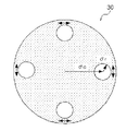
次に、上記マスク10を用いて露光を行い、ウエハ上にパターンを形成するパターン形成方法について説明する。ここでは、縮小倍率4倍のArF露光装置(露光波長λ=193nm、NA=0.92)を使用し、図3に示す輪帯照明20を適用してマスク10に対して照明を行った。輪帯照明20は、例えば、遮光率75%であって、光学条件をσout=0.95、σin=0.7125とした。さらに、輪帯照明20では、マスク10に対して、アジマーサル偏光を照明し、また、偏光していない光を照明した。アジマーサル偏光は、直線偏光であって、偏光方向が、同図の矢印で示す方向、即ち輪帯照明20を構成する2次光源の半径方向に垂直である方向となる。
Next, a pattern forming method in which exposure is performed using the
以下、表1を用いて、マスク10を用いたパターン形成方法による、レジストパターンの解像特性を、ホールパターン1のNILS(Normalized Image log-slope)値で示した。レジストの反応は、光強度のlog値に比例することが知られており、そのため、光強度のlog値の傾きが、レジストパターン解像を判定するパラメータ、即ちILS(イメージ・ログ・スロープ)として用いられている。そこで以下では、パターン寸法が異なっても、レジストパターン解像を同じように判定できるようにILSを規格化したNILS値を用いて解像特性を示した。NILS値は、通常、値が1.0程度あれば、ウエハ上に、良好なレジストパターンが形成できると判断される。なお、NILS値は、光強度のlog値の傾きに自身のパターン寸法を掛けて規格化される。
Hereinafter, with reference to Table 1, the resolution characteristics of the resist pattern by the pattern forming method using the
表1には、本実施形態のマスク10での、X及びY方向のピッチが140nm〜200nmであるホールパターン1のNISL値と、比較例1であるクロム遮光マスク(透過率0%)のNILS値と、比較例2である従来のハーフトーンマスク(透過率6%)のNILS値と、をそれぞれ示している。さらに、本実施形態のマスク10、比較例1,2のマスク共に、輪帯照明20からアジマーサル偏光(偏光有り)を照明したり、偏光のない光(偏光無し)を照明したりして、それぞれの場合でのNILS値を示した。
Table 1 shows the NISL value of the

これに対して、本実施形態のマスク10では、ホールパターン1の周辺であって、ピッチの狭いXY方向をハーフトーン位相シフト領域(透過率2〜20%であるが、ここでは、6%とした)からなる周辺領域2aとした。また、ピッチの緩い斜め45/135度方向の領域を遮光領域(透過率0%)からなる周辺領域2bとした。更に、アジマーサル偏光を照明することにより、140〜180nmのピッチにおいて、比較例1,2のマスクと比べて、大きなNILS値を得ることができた。これは、以下のように考えられる。
On the other hand, in the
つまり、マスク10では、ホールパターン1の周辺を、周辺領域2aと周辺領域2bとに区分し、それぞれの周辺領域2a,2bで入射光に逆位相を与えるか否か、及び透過率の大きさを個別に規定して、高いNILS値が得られるように最適化している。その結果、ホールパターン1の中心からのXY方向、斜め45/135度方向に沿った距離に対して、マスク透過光の振幅分布がいわゆるベッセル関数に近似されたためと考えられる。
That is, in the
なお、ピッチが200nm以上であれば、ホールパターン1のコーナー間に図示しない補助パターンを配置して、補助パターンにより2光束干渉の結像状態に近づけて、NILS値を改善することができる。よって、本発明の適用範囲は、露光光の波長以下のピッチとなる。
If the pitch is 200 nm or more, an auxiliary pattern (not shown) is arranged between the corners of the
(第2の実施形態)
図4は、本発明の第2の実施形態に係る露光用マスクを示す平面図である。以下では図1に示したマスク10と構成や機能等が重複する部分は適宜説明を省略する。マスク10Aは、ホールパターン11と、周辺領域12a,12bとを備える。ホールパターン11は、例えば、正方形であって、露光光の限界解像度以上の寸法(W=50nm)を有し、互いに直交するX方向及びY方向に一定ピッチ(P=140nm)で繰り返し配置され、入射光に逆位相を与えるハーフトーン位相シフト領域からなる。
(Second Embodiment)
FIG. 4 is a plan view showing an exposure mask according to the second embodiment of the present invention. In the following, the description of the portions where the configuration and functions overlap with those of the
周辺領域12aは、例えば、長方形(長辺が90nm、短辺が50nm)であり、X方向及びY方向に隣接する2つのホールパターン11の間に配置された遮光領域(透過率が0%)からなる。周辺領域12bは、例えば、正方形(一辺が90nm)であり、斜め45/135度方向に隣接する2つのホールパターン11の間に配置されたハーフトーン領域からなる。但し、周辺領域12bでは、透過率が30%以上であることが好ましく、単にハーフトーン領域ではなく、透明領域も含むことになる。
The
次に、上記マスク10Aを用いて露光を行い、ウエハ上にXY方向のピッチ140nm、幅寸法70nmのドットパターンを形成するパターン形成方法について説明する。ここでは、縮小倍率4倍のArF露光装置(露光波長λ=193nm、NA=0.86)を使用し、図5に示すクロスポール照明30を適用してマスク10Aに対して照明を行った。
Next, a pattern forming method for performing exposure using the
クロスポール照明30は、例えば、光学条件をσc=0.8、σr=0.1、XY偏光有りとした。さらに、クロスポール照明30では、マスク10Aに対して、同図の矢印で示す偏光方向のXY偏光を照明した。XY偏光では、相互に対向する2つの2次光源が2組配置されたクロスポール照明30から得られ、かつ、各2次光源が、対応して配置される2次光源に対向する方向と垂直方向に偏光している。
For the
クロスポール照明30は、いわゆる4点照明であって、焦点深度より解像力を重視した照明とされ、必要最小限の焦点深度しか得られない代わりに、最も微細なXY方向の繰り返しパターンをウエハ上に形成できる。クロスポール照明30は、解像特性の方向依存性が顕著であり、例えば、XY方向の解像特性と斜め45/135度方向の解像特性とは異なる。マスク10Aでは、上記マスク10と同様に、ピッチP=140nmとし、ホールパターン11の周辺領域を、XY方向の周辺領域12aと、45/135度方向の周辺領域12bに区分して、それそれの透過率及び位相を最適化した。
The
以下では、ホールパターン11を、幅寸法W=50nm、透過率12%、位相差180度のハーフトーン位相シフト領域とし、更に、周辺領域12a,12bの位相をいずれも0度とした上で、周辺領域12a,12bの透過率をパラメータとして、NILS値が大きくなる条件を求めた。
In the following, the
図6は、図4に示すマスク10Aを用いて露光を行い、ウエハ上に幅寸法70nmのドットパターンを形成した際のNILS値(X軸上)の計算結果を示すグラフである。同図では、横軸を周辺領域12aの透過率とし、縦軸を周辺領域12bの透過率とした。さらに、グラフ上で、幅寸法70nmのドットパターンのNILS値を、−1.0〜4.0の範囲を1.0毎に区分して示している。同図のグラフでは、周辺領域12aの透過率が0%あるとき、NILS値が大きくなっていることがわかる。
FIG. 6 is a graph showing the calculation result of the NILS value (on the X axis) when exposure is performed using the
図7は、図6に示すグラフに基づいて、周辺領域12aの透過率が0%であるときのNILS値を示している。つまり、このグラフは、周辺領域12aの透過率が0%であるときの縦軸上の値を抜き出して示している。同図に示すように、周辺領域12aの透過率が0%であって、周辺領域12bの透過率=34%以上であるときに、NILS値が3.0以上となっている。但し、周辺領域12bの透過率は、34%以上に限定されず、パターン11の寸法が、パターン11に対応してウエハ上に形成されるドットパターンの寸法よりも小さく、かつ、パターン11の透過率が2〜20%のときに、周辺領域12bの透過率が30%以上であることが好ましい。
FIG. 7 shows the NILS value when the transmittance of the
ここで、マスク10Aの製造工程を考慮すると、2種類の透過率領域、即ちハーフトーン位相シフト領域からなるホールパターン11と、周辺領域12bとを作成し、その2種類とも位相差を制御するので、ハーフトーンマスクの成膜条件を最適化する必要が生じる。ここで、ホールパターン11は、位相差180度であり、また、周辺領域12bは、位相差0度である。ArF露光でのハーフトーン領域の透過率は6%が標準的な値であるが、2〜20%程度まであれば成膜条件が確立されている。そこで、周辺領域12bの透過率が例えば30%以上であれば、図7に示すNILSの値が略同一であるから、周辺領域12bは、透過率が100%である透明領域とすれば、マスク10Aを容易に製造でき、実用的に好ましい。なお、ここではホールパターン11をハーフトーン位相シフト領域として、周辺領域12a,12bの透過率及び位相を最適化したが、これに限定されず、ホールパターン11を遮光領域や透明領域としてもよい。
Here, considering the manufacturing process of the
(第3の実施形態)
図8は、本発明の第3の実施形態に係る露光マスクを用いて露光を行い、ウエハ上に70nmのドットパターンを形成した際のNILS値の計算結果を示すグラフである。
本実施形態のマスクは、図示しないが、幅寸法W=50nm、透過率100%、位相差0の透明領域からなるホールパターンと、ホールパターンの第1及び第2の周辺領域とを有する。第1の周辺領域は、透過率6%、位相差180度のハーフトーン位相シフト領域からなり、X方向及びY方向に隣接する2つのホールパターンの間に配置される。第2の周辺領域は、透過率0〜100%、位相差180度の位相シフト領域からなり、
斜め45/135度方向に隣接する2つのホールパターンの間に配置される。なお、ここでのマスクは、ホールパターンのピッチPを、上記マスク10Aと同様に140nmとし、さらに、図5に示すクロスポール照明30を適用して直線偏光を照明した。
(Third embodiment)
FIG. 8 is a graph showing a calculation result of the NILS value when exposure is performed using the exposure mask according to the third embodiment of the present invention and a dot pattern of 70 nm is formed on the wafer.
Although not shown, the mask of this embodiment includes a hole pattern made of a transparent region having a width dimension W = 50 nm, a transmittance of 100%, and a phase difference of 0, and first and second peripheral regions of the hole pattern. The first peripheral region is a halftone phase shift region having a transmittance of 6% and a phase difference of 180 degrees, and is arranged between two hole patterns adjacent in the X direction and the Y direction. The second peripheral region is composed of a phase shift region having a transmittance of 0 to 100% and a phase difference of 180 degrees,
It is arranged between two hole patterns adjacent in the oblique 45/135 degree direction. The mask here has a hole pattern pitch P of 140 nm, similar to the
同図では、横軸を第1の周辺領域の透過率とし、縦軸を第2の周辺領域の透過率として、NILS値を等高線で示している。このグラフによれば、NILS値が3.0以上となる領域40は広く、例えば、第2の周辺領域の透過率が、第1の周辺領域の透過率に応じて0〜100%の範囲を採ることができる。特に、第1の周辺領域の透過率が6%、第2の周辺領域の透過率が100%のときに、NILS値が3.04となり、大きな値を得ることができた。
In the figure, the horizontal axis is the transmittance of the first peripheral region, the vertical axis is the transmittance of the second peripheral region, and the NILS value is indicated by contour lines. According to this graph, the
従って、本実施形態でのマスクに対して、斜入射照明法で直線偏光を照明することで、広い範囲で解像特性を向上できたことがわかる。これは、上記マスク10,10Aと同様に、ホールパターンの中心からのXY方向、斜め45/135度方向に沿った距離に対して、マスク透過光の振幅分布がいわゆるベッセル関数に近似されたためと考えられる。
Therefore, it can be seen that the resolution characteristics can be improved in a wide range by irradiating the linearly polarized light by the oblique incidence illumination method with respect to the mask in the present embodiment. This is because, similar to the
上記第1の実施形態に係るマスク10では、周辺領域2bを遮光領域にするために遮光膜5(図2(b)参照)を用いたが、これに限定されず、周辺領域2bをハーフトーン膜4のみとし、その中央に微細な開口パターンを形成してもよい。この構成により、微細な開口パターンの透過光とハーフトーン膜4の透過光とは位相差が180度となり、互いに打ち消し合い、遮光領域と見なせるようになる。
In the
また、上記開口パターンは、2光束干渉の結像状態を形成するための補助パターンより寸法が小さいことが好ましい。具体的には、補助パターンは、ピッチPが200nm以上で繰り返し配列されたホールパターン周辺に配置することが可能であり、自身が明部となるように、その寸法をホールパターンの2/3程度の寸法である60nmとすればよい。一方、上記開口パターンは、寸法が大きすぎると、斜め45/135度方向のピッチが露光装置の限界解像度を超えてしまい、焦点深度が低下するという悪影響が生じてしまう。そこで、開口パターンの寸法は、ホールパターンの1/2以下の40nm程度にすればよい。 The opening pattern preferably has a smaller dimension than the auxiliary pattern for forming an image formation state of two-beam interference. Specifically, the auxiliary pattern can be arranged around a hole pattern that is repeatedly arranged with a pitch P of 200 nm or more, and the dimension of the auxiliary pattern is about 2/3 of the hole pattern so as to be a bright part. It is sufficient to set the size to 60 nm. On the other hand, if the size of the opening pattern is too large, the pitch in the oblique 45/135 degree direction exceeds the limit resolution of the exposure apparatus, which causes an adverse effect that the depth of focus is lowered. Therefore, the dimension of the opening pattern may be about 40 nm which is 1/2 or less of the hole pattern.
また、上記各実施形態では、ArFエキシマレーザー露光に用いられる透過型マスクについて説明したが、これに限定されず、他の波長や反射型マスク、即ち積層の反射ミラーに吸収材料でパターンを形成したマスク等にも適用できる。 In each of the above embodiments, the transmission type mask used for ArF excimer laser exposure has been described. However, the present invention is not limited to this, and other wavelengths and reflection type masks, that is, a pattern is formed of an absorbing material on a reflective mirror in a stack. It can also be applied to masks.
さらに、上記各実施形態では、ホールパターンが一定ピッチPで、X方向及びY方向に繰り返し配置される例を示したが、これに限定されない。即ち、2つのホールパターンが近付くような、多少ずれた繰り返しで配置されていてもよい。 Further, in each of the above embodiments, the example in which the hole pattern is repeatedly arranged in the X direction and the Y direction at a constant pitch P is shown, but the present invention is not limited to this. In other words, the two hole patterns may be arranged so as to be slightly shifted so as to approach each other.
以上説明したように、本発明の露光用マスク及びパターン形成方法によると、以下の態様の採用が可能である。第1の態様の露光用マスクで、半透明領域(2a)の透過率が、2〜20%であることが好ましい。この場合に、斜入射照明法により直線偏光を照明することで、解像特性を向上できる。 As described above, according to the exposure mask and pattern formation method of the present invention, the following modes can be adopted. In the exposure mask of the first aspect, it is preferable that the transmissivity of the translucent region (2a) is 2 to 20%. In this case, the resolution characteristic can be improved by illuminating the linearly polarized light by the oblique incidence illumination method.
第2の態様の露光用マスクで、半透明領域(11)の寸法(W)が、半透明領域に対応してウエハ上に形成されるパターンの寸法よりも小さく、かつ、半透明領域の透過率が2〜20%のときに、第3の方向に隣接する2つの矩形状パターンの間に配置された領域(12b)の透過率が30%以上であることが好ましい。この場合に、斜入射照明法により直線偏光を照明することで、いわゆるNILS値が3.0を超えるので、解像特性を向上できる。 In the exposure mask according to the second aspect, the dimension (W) of the translucent area (11) is smaller than the dimension of the pattern formed on the wafer corresponding to the translucent area, and the translucent area is transmitted. When the rate is 2 to 20%, the transmittance of the region (12b) disposed between the two rectangular patterns adjacent in the third direction is preferably 30% or more. In this case, since the so-called NILS value exceeds 3.0 by illuminating the linearly polarized light by the oblique incidence illumination method, the resolution characteristic can be improved.
第3の態様の露光用マスクで、位相シフト領域の透過率が、半透明領域の透過率に応じて0〜100%の範囲となることが好ましい。この場合に、斜入射照明法で直線偏光を照明することで、広い範囲でNILS値を3.0以上とすることができ、解像特性を向上できる。 In the exposure mask according to the third aspect, the transmittance of the phase shift region is preferably in the range of 0 to 100% depending on the transmittance of the translucent region. In this case, by illuminating the linearly polarized light by the oblique incidence illumination method, the NILS value can be 3.0 or more in a wide range, and the resolution characteristics can be improved.
第3の方向は、第1の方向及び第2の方向のそれぞれから45度の角度方向にあることが好ましい。露光用マスクは、DRAM等の各種メモリの製造に用いられる。また、矩形状パターンが繰り返し配置されるピッチが、露光光の波長以下であることが好ましい。 The third direction is preferably at an angular direction of 45 degrees from each of the first direction and the second direction. The exposure mask is used for manufacturing various memories such as a DRAM. Moreover, it is preferable that the pitch at which the rectangular pattern is repeatedly arranged is equal to or less than the wavelength of the exposure light.
直線偏光が、輪帯照明(20)を構成する2次光源から得られ、かつ、偏光方向が2次光源の半径方向に垂直である。この場合の斜入射照明は、輪帯照明となる。 Linearly polarized light is obtained from the secondary light source that constitutes the annular illumination (20), and the polarization direction is perpendicular to the radial direction of the secondary light source. The oblique incident illumination in this case is annular illumination.
直線偏光が、相互に対向する2つの2次光源が2組配置されたクロスポール照明(30)から得られ、かつ、各2次光源が、対応して配置される2次光源に対向する方向と垂直方向に偏光している。この場合の斜入射照明は、クロスポール照明となる。 A direction in which linearly polarized light is obtained from cross pole illumination (30) in which two sets of two secondary light sources facing each other are arranged, and each secondary light source faces a corresponding secondary light source. And polarized vertically. The oblique incidence illumination in this case is cross pole illumination.
以上、本発明をその好適な実施形態に基づいて説明したが、本発明の露光用マスク及びパターン形成方法は、上記実施形態の構成にのみ限定されるものではなく、上記実施形態の構成から種々の修正及び変更を施したものも、本発明の範囲に含まれる。 Although the present invention has been described based on the preferred embodiment, the exposure mask and the pattern forming method of the present invention are not limited to the configuration of the above-described embodiment, and various modifications can be made from the configuration of the above-described embodiment. Those modified and changed as described above are also included in the scope of the present invention.
1,11:ホールパターン
2a,2b,12a,12b:周辺領域
3:透明基板
4:ハーフトーン膜
5:遮光膜
20:輪帯照明
30:クロスポール照明
40:領域
10,10A:露光用マスク
DESCRIPTION OF
Claims (10)
前記複数の第1のハーフトーン位相シフト領域のうち、前記第1の方向及び前記第2の方向に隣接する各2つの第1のハーフトーン位相シフト領域の間に配置された長方形パターンからなり、前記入射光を遮光する複数の第1の周辺領域と、
前記複数の第1のハーフトーン位相シフト領域のうち、前記第1の方向及び前記第2の方向とは異なる第3の方向に隣接する各2つの第1のハーフトーン位相シフト領域の間に配置された第2の正方形パターンからなる複数の第2の周辺領域と、を有することを特徴とする露光用マスク。 A plurality of first square patterns having a dimension equal to or higher than the limit resolution of the exposure light and repeatedly arranged at a constant pitch in a first direction and a second direction substantially orthogonal to each other , and giving an antiphase to incident light A first halftone phase shift region ;
Wherein the plurality of first of the halftone phase shift region, the Ri first direction and Tona said second rectangular pattern disposed between each two first halftone phase shift region adjacent to the direction A plurality of first peripheral regions that block the incident light ; and
Among the plurality of first halftone phase shift regions , the first halftone phase shift region is arranged between each two first halftone phase shift regions adjacent to each other in a third direction different from the first direction and the second direction. it has been a second exposure mask, characterized in that it comprises a plurality of second peripheral region consisting square pattern.
前記露光用マスクに対して、斜入射照明法により直線偏光を照明することを特徴とするパターン形成方法。 Subjected to exposure using an exposure mask according to claim 1 to 7, a pattern forming method for forming a pattern on a wafer,
A pattern forming method, wherein the exposure mask is irradiated with linearly polarized light by an oblique incidence illumination method.
Priority Applications (2)
| Application Number | Priority Date | Filing Date | Title |
|---|---|---|---|
| JP2008028381A JP5571289B2 (en) | 2008-02-08 | 2008-02-08 | Exposure mask and pattern forming method |
| US12/366,219 US7923179B2 (en) | 2008-02-08 | 2009-02-05 | Exposure mask and pattern forming method therefor |
Applications Claiming Priority (1)
| Application Number | Priority Date | Filing Date | Title |
|---|---|---|---|
| JP2008028381A JP5571289B2 (en) | 2008-02-08 | 2008-02-08 | Exposure mask and pattern forming method |
Publications (3)
| Publication Number | Publication Date |
|---|---|
| JP2009186863A JP2009186863A (en) | 2009-08-20 |
| JP2009186863A5 JP2009186863A5 (en) | 2011-05-26 |
| JP5571289B2 true JP5571289B2 (en) | 2014-08-13 |
Family
ID=40939164
Family Applications (1)
| Application Number | Title | Priority Date | Filing Date |
|---|---|---|---|
| JP2008028381A Expired - Fee Related JP5571289B2 (en) | 2008-02-08 | 2008-02-08 | Exposure mask and pattern forming method |
Country Status (2)
| Country | Link |
|---|---|
| US (1) | US7923179B2 (en) |
| JP (1) | JP5571289B2 (en) |
Families Citing this family (5)
| Publication number | Priority date | Publication date | Assignee | Title |
|---|---|---|---|---|
| JP5708082B2 (en) * | 2010-03-24 | 2015-04-30 | 信越化学工業株式会社 | Pattern forming method and negative resist composition |
| JP5533797B2 (en) * | 2010-07-08 | 2014-06-25 | 信越化学工業株式会社 | Pattern formation method |
| CN105607349B (en) * | 2016-03-14 | 2019-01-11 | 深圳市华星光电技术有限公司 | PI liquid coating method |
| US10847482B2 (en) | 2018-05-16 | 2020-11-24 | Micron Technology, Inc. | Integrated circuit structures and methods of forming an opening in a material |
| US10651100B2 (en) | 2018-05-16 | 2020-05-12 | Micron Technology, Inc. | Substrates, structures within a scribe-line area of a substrate, and methods of forming a conductive line of a redistribution layer of a substrate and of forming a structure within a scribe-line area of the substrate |
Family Cites Families (11)
| Publication number | Priority date | Publication date | Assignee | Title |
|---|---|---|---|---|
| JPH07281413A (en) * | 1994-04-05 | 1995-10-27 | Mitsubishi Electric Corp | Attenuation type phase shift mask and its production |
| US5840447A (en) * | 1997-08-29 | 1998-11-24 | International Business Machines Corporation | Multi-phase photo mask using sub-wavelength structures |
| JP3275863B2 (en) * | 1999-01-08 | 2002-04-22 | 日本電気株式会社 | Photo mask |
| US6887633B2 (en) * | 2002-02-08 | 2005-05-03 | Chih-Hsien Nail Tang | Resolution enhancing technology using phase assignment bridges |
| JP3754378B2 (en) * | 2002-02-14 | 2006-03-08 | 株式会社ルネサステクノロジ | Manufacturing method of semiconductor integrated circuit device |
| US20030180629A1 (en) * | 2002-03-20 | 2003-09-25 | Nanya Technology Corporation | Masks and method for contact hole exposure |
| JP3651676B2 (en) * | 2002-07-11 | 2005-05-25 | 株式会社東芝 | Inspection method and photomask |
| JP3958163B2 (en) * | 2002-09-19 | 2007-08-15 | キヤノン株式会社 | Exposure method |
| JP4684584B2 (en) * | 2003-07-23 | 2011-05-18 | キヤノン株式会社 | Mask, manufacturing method thereof, and exposure method |
| US7354682B1 (en) * | 2004-07-09 | 2008-04-08 | Advanced Micro Devices, Inc. | Chromeless mask for contact holes |
| US7556891B2 (en) * | 2004-10-25 | 2009-07-07 | Chartered Semiconductor Manufacturing Ltd. | Method and apparatus for contact hole unit cell formation |
-
2008
- 2008-02-08 JP JP2008028381A patent/JP5571289B2/en not_active Expired - Fee Related
-
2009
- 2009-02-05 US US12/366,219 patent/US7923179B2/en not_active Expired - Fee Related
Also Published As
| Publication number | Publication date |
|---|---|
| JP2009186863A (en) | 2009-08-20 |
| US7923179B2 (en) | 2011-04-12 |
| US20090202926A1 (en) | 2009-08-13 |
Similar Documents
| Publication | Publication Date | Title |
|---|---|---|
| US7569312B2 (en) | Mask data creation method | |
| JP3574417B2 (en) | Optical proximity correction | |
| JP4646367B2 (en) | Semiconductor device manufacturing method and semiconductor device | |
| JPH08316125A (en) | Method and apparatus for projection exposing | |
| JPH08316124A (en) | Method and apparatus for projection exposing | |
| US5642183A (en) | Spatial filter used in a reduction-type projection printing apparatus | |
| JP2006221078A (en) | Photomask, method for producing mask pattern, and method for forming pattern of semiconductor device | |
| JP2009043789A (en) | Pattern forming method, and mask | |
| JP5571289B2 (en) | Exposure mask and pattern forming method | |
| US20110122394A1 (en) | Computer readable storage medium including effective light source calculation program, and exposure method | |
| JP2001272764A (en) | Photomask for projection exposure and for projection exposure method using the photomask | |
| US20030035089A1 (en) | Method for improved resolution of patterning using binary masks with pupil filters | |
| JP5524447B2 (en) | Exposure mask, pattern forming method, and exposure mask manufacturing method | |
| JP3347670B2 (en) | Mask and exposure method using the same | |
| JP3303077B2 (en) | Mask and pattern forming method | |
| JP2004251969A (en) | Phase shift mask, method for forming pattern by using phase shift mask, and method for manufacturing electronic device | |
| JP2007018005A (en) | Photomask | |
| JPH09120154A (en) | Polarizing mask and its production as well as pattern exposure method and pattern projection aligner using the same | |
| JP3967359B2 (en) | Pattern formation method | |
| JP2008191364A (en) | Design method of mask pattern | |
| JP4314285B2 (en) | Photo mask | |
| JP3133618B2 (en) | Spatial filter used in reduction projection exposure apparatus | |
| JP5068357B2 (en) | Semiconductor device manufacturing method, photomask pattern design method, and photomask manufacturing method | |
| JPH07211617A (en) | Pattern formation, mask and projection aligner | |
| JPH10115932A (en) | Exposure method using phase shift mask |
Legal Events
| Date | Code | Title | Description |
|---|---|---|---|
| RD01 | Notification of change of attorney |
Free format text: JAPANESE INTERMEDIATE CODE: A7421 Effective date: 20100205 |
|
| A621 | Written request for application examination |
Free format text: JAPANESE INTERMEDIATE CODE: A621 Effective date: 20101108 |
|
| A521 | Written amendment |
Free format text: JAPANESE INTERMEDIATE CODE: A523 Effective date: 20110407 |
|
| A711 | Notification of change in applicant |
Free format text: JAPANESE INTERMEDIATE CODE: A711 Effective date: 20130730 |
|
| A521 | Written amendment |
Free format text: JAPANESE INTERMEDIATE CODE: A523 Effective date: 20130822 |
|
| A131 | Notification of reasons for refusal |
Free format text: JAPANESE INTERMEDIATE CODE: A131 Effective date: 20130917 |
|
| A601 | Written request for extension of time |
Free format text: JAPANESE INTERMEDIATE CODE: A601 Effective date: 20131209 |
|
| A602 | Written permission of extension of time |
Free format text: JAPANESE INTERMEDIATE CODE: A602 Effective date: 20131212 |
|
| A521 | Written amendment |
Free format text: JAPANESE INTERMEDIATE CODE: A523 Effective date: 20140317 |
|
| TRDD | Decision of grant or rejection written | ||
| A01 | Written decision to grant a patent or to grant a registration (utility model) |
Free format text: JAPANESE INTERMEDIATE CODE: A01 Effective date: 20140527 |
|
| A61 | First payment of annual fees (during grant procedure) |
Free format text: JAPANESE INTERMEDIATE CODE: A61 Effective date: 20140626 |
|
| R150 | Certificate of patent or registration of utility model |
Ref document number: 5571289 Country of ref document: JP Free format text: JAPANESE INTERMEDIATE CODE: R150 |
|
| LAPS | Cancellation because of no payment of annual fees |