JP5570210B2 - Optically effective surface relief microstructure and manufacturing method thereof - Google Patents
Optically effective surface relief microstructure and manufacturing method thereof Download PDFInfo
- Publication number
- JP5570210B2 JP5570210B2 JP2009508082A JP2009508082A JP5570210B2 JP 5570210 B2 JP5570210 B2 JP 5570210B2 JP 2009508082 A JP2009508082 A JP 2009508082A JP 2009508082 A JP2009508082 A JP 2009508082A JP 5570210 B2 JP5570210 B2 JP 5570210B2
- Authority
- JP
- Japan
- Prior art keywords
- surface relief
- relief
- microstructure
- mask
- zone
- Prior art date
- Legal status (The legal status is an assumption and is not a legal conclusion. Google has not performed a legal analysis and makes no representation as to the accuracy of the status listed.)
- Active
Links
Images


Classifications
-
- B—PERFORMING OPERATIONS; TRANSPORTING
- B29—WORKING OF PLASTICS; WORKING OF SUBSTANCES IN A PLASTIC STATE IN GENERAL
- B29D—PRODUCING PARTICULAR ARTICLES FROM PLASTICS OR FROM SUBSTANCES IN A PLASTIC STATE
- B29D11/00—Producing optical elements, e.g. lenses or prisms
- B29D11/00865—Applying coatings; tinting; colouring
-
- G—PHYSICS
- G02—OPTICS
- G02B—OPTICAL ELEMENTS, SYSTEMS OR APPARATUS
- G02B5/00—Optical elements other than lenses
- G02B5/02—Diffusing elements; Afocal elements
- G02B5/0205—Diffusing elements; Afocal elements characterised by the diffusing properties
- G02B5/021—Diffusing elements; Afocal elements characterised by the diffusing properties the diffusion taking place at the element's surface, e.g. by means of surface roughening or microprismatic structures
- G02B5/0221—Diffusing elements; Afocal elements characterised by the diffusing properties the diffusion taking place at the element's surface, e.g. by means of surface roughening or microprismatic structures the surface having an irregular structure
-
- B—PERFORMING OPERATIONS; TRANSPORTING
- B42—BOOKBINDING; ALBUMS; FILES; SPECIAL PRINTED MATTER
- B42D—BOOKS; BOOK COVERS; LOOSE LEAVES; PRINTED MATTER CHARACTERISED BY IDENTIFICATION OR SECURITY FEATURES; PRINTED MATTER OF SPECIAL FORMAT OR STYLE NOT OTHERWISE PROVIDED FOR; DEVICES FOR USE THEREWITH AND NOT OTHERWISE PROVIDED FOR; MOVABLE-STRIP WRITING OR READING APPARATUS
- B42D25/00—Information-bearing cards or sheet-like structures characterised by identification or security features; Manufacture thereof
- B42D25/20—Information-bearing cards or sheet-like structures characterised by identification or security features; Manufacture thereof characterised by a particular use or purpose
- B42D25/29—Securities; Bank notes
-
- B—PERFORMING OPERATIONS; TRANSPORTING
- B42—BOOKBINDING; ALBUMS; FILES; SPECIAL PRINTED MATTER
- B42D—BOOKS; BOOK COVERS; LOOSE LEAVES; PRINTED MATTER CHARACTERISED BY IDENTIFICATION OR SECURITY FEATURES; PRINTED MATTER OF SPECIAL FORMAT OR STYLE NOT OTHERWISE PROVIDED FOR; DEVICES FOR USE THEREWITH AND NOT OTHERWISE PROVIDED FOR; MOVABLE-STRIP WRITING OR READING APPARATUS
- B42D25/00—Information-bearing cards or sheet-like structures characterised by identification or security features; Manufacture thereof
- B42D25/30—Identification or security features, e.g. for preventing forgery
- B42D25/324—Reliefs
-
- B—PERFORMING OPERATIONS; TRANSPORTING
- B42—BOOKBINDING; ALBUMS; FILES; SPECIAL PRINTED MATTER
- B42D—BOOKS; BOOK COVERS; LOOSE LEAVES; PRINTED MATTER CHARACTERISED BY IDENTIFICATION OR SECURITY FEATURES; PRINTED MATTER OF SPECIAL FORMAT OR STYLE NOT OTHERWISE PROVIDED FOR; DEVICES FOR USE THEREWITH AND NOT OTHERWISE PROVIDED FOR; MOVABLE-STRIP WRITING OR READING APPARATUS
- B42D25/00—Information-bearing cards or sheet-like structures characterised by identification or security features; Manufacture thereof
- B42D25/30—Identification or security features, e.g. for preventing forgery
- B42D25/328—Diffraction gratings; Holograms
-
- B—PERFORMING OPERATIONS; TRANSPORTING
- B42—BOOKBINDING; ALBUMS; FILES; SPECIAL PRINTED MATTER
- B42D—BOOKS; BOOK COVERS; LOOSE LEAVES; PRINTED MATTER CHARACTERISED BY IDENTIFICATION OR SECURITY FEATURES; PRINTED MATTER OF SPECIAL FORMAT OR STYLE NOT OTHERWISE PROVIDED FOR; DEVICES FOR USE THEREWITH AND NOT OTHERWISE PROVIDED FOR; MOVABLE-STRIP WRITING OR READING APPARATUS
- B42D25/00—Information-bearing cards or sheet-like structures characterised by identification or security features; Manufacture thereof
- B42D25/40—Manufacture
- B42D25/405—Marking
- B42D25/43—Marking by removal of material
- B42D25/445—Marking by removal of material using chemical means, e.g. etching
-
- G—PHYSICS
- G02—OPTICS
- G02B—OPTICAL ELEMENTS, SYSTEMS OR APPARATUS
- G02B5/00—Optical elements other than lenses
- G02B5/02—Diffusing elements; Afocal elements
- G02B5/0205—Diffusing elements; Afocal elements characterised by the diffusing properties
- G02B5/0257—Diffusing elements; Afocal elements characterised by the diffusing properties creating an anisotropic diffusion characteristic, i.e. distributing output differently in two perpendicular axes
-
- G—PHYSICS
- G02—OPTICS
- G02B—OPTICAL ELEMENTS, SYSTEMS OR APPARATUS
- G02B5/00—Optical elements other than lenses
- G02B5/02—Diffusing elements; Afocal elements
- G02B5/0205—Diffusing elements; Afocal elements characterised by the diffusing properties
- G02B5/0263—Diffusing elements; Afocal elements characterised by the diffusing properties with positional variation of the diffusing properties, e.g. gradient or patterned diffuser
-
- G—PHYSICS
- G02—OPTICS
- G02B—OPTICAL ELEMENTS, SYSTEMS OR APPARATUS
- G02B5/00—Optical elements other than lenses
- G02B5/02—Diffusing elements; Afocal elements
- G02B5/0268—Diffusing elements; Afocal elements characterized by the fabrication or manufacturing method
-
- G—PHYSICS
- G02—OPTICS
- G02B—OPTICAL ELEMENTS, SYSTEMS OR APPARATUS
- G02B5/00—Optical elements other than lenses
- G02B5/02—Diffusing elements; Afocal elements
- G02B5/0273—Diffusing elements; Afocal elements characterized by the use
- G02B5/0284—Diffusing elements; Afocal elements characterized by the use used in reflection
Landscapes
- Physics & Mathematics (AREA)
- General Physics & Mathematics (AREA)
- Optics & Photonics (AREA)
- Engineering & Computer Science (AREA)
- Manufacturing & Machinery (AREA)
- Business, Economics & Management (AREA)
- Accounting & Taxation (AREA)
- Finance (AREA)
- Chemical & Material Sciences (AREA)
- Chemical Kinetics & Catalysis (AREA)
- General Chemical & Material Sciences (AREA)
- Health & Medical Sciences (AREA)
- Ophthalmology & Optometry (AREA)
- Mechanical Engineering (AREA)
- Diffracting Gratings Or Hologram Optical Elements (AREA)
- Credit Cards Or The Like (AREA)
- Moulds For Moulding Plastics Or The Like (AREA)
Description
本発明は、たとえば偽造及び変造に対して書類及び物品を安全保障するために使用することができる、特徴的な色外観を有する光学装置に関する。 The present invention relates to an optical device having a characteristic color appearance that can be used, for example, to secure documents and articles against counterfeiting and alteration.
より具体的には、本発明は、光学的に有効な表面レリーフ微細構造を有する少なくとも一つの表面区域を有する要素及び当該要素の製造方法に関する。 More specifically, the present invention relates to an element having at least one surface area with an optically effective surface relief microstructure and a method of manufacturing the element.
発明の背景
偽造、不正改造に対する防護及び製品保護一般のための光学装置の使用は今や十分に確立された技術である。
BACKGROUND OF THE INVENTION The use of optical devices for protection against counterfeiting, tampering and product protection in general is now a well established technology.
詐欺行為及び偽造の増加のせいで、新規な対偽造手段が絶えず求められている。長年、ホログラムが好ましい安全保障技術であった。そうこうするうち、この技術は30年余りを経過し、したがって、周知であり、広まっている。ホログラフィーフォイルは今やどのギフトショップででも見つけることができる。多くの人々がホログラム技術を手に入れることができるため、この状況は安全保障の危険を表す。デジタルホログラムプリンタが利用可能になるとともに、使いやすいホログラフィーマスタリングシステムへの道がさらに開かれた。このようなプリンタは、多くの異なるタイプのホログラムの製造を可能にし、ホログラフィーセットアップ又はレーザライタの知識は最小限しか要らない。このような設備は、後続のメタルマスタ製造のためのマスタの調製及び薄膜への大量複製を可能にする。 Due to fraud and increased counterfeiting, new counterfeiting measures are constantly being sought. For many years, holograms have been the preferred security technology. In the meantime, this technology has passed over 30 years and is therefore well known and widespread. Holographic foil can now be found in any gift shop. This situation represents a security risk as many people have access to hologram technology. With the availability of digital hologram printers, the path to easy-to-use holography mastering systems has further opened. Such printers allow the production of many different types of holograms, with minimal knowledge of holographic setups or laser writers. Such equipment allows the preparation of masters for subsequent metal master production and mass replication to thin films.
したがって、ホログラフィー装置から明確に区別可能である新規な安全保障機能によって安全保障装置のパレットを拡張することが非常に望ましい。そのような新規な装置の例が代替の光学可変装置(OVD)である。OVDとは、視角又は照明角が変化するとともに外観を変化させる装置である。OVDのサブグループがカラーシフト装置である。カラーシフトOVDは、視角又は照明角が変化するとともに色を変化させる。顕著な代表的カラーシフトOVDは、コレステリック又は干渉膜及びそのような膜のフレークに基づく光学装置である。いずれも、装置が垂直な視角に対して傾くとともに顕著なカラーシフトを示す。標準的な量産ホログラフィー装置の特徴である虹色は、これらのタイプのカラーシフト装置では見られない。 Therefore, it is highly desirable to extend the pallet of the security device with a new security feature that is clearly distinguishable from the holographic device. An example of such a novel device is an alternative optical variable device (OVD). OVD is a device that changes the appearance as the viewing angle or illumination angle changes. A subgroup of OVD is a color shift device. The color shift OVD changes the color as the viewing angle or illumination angle changes. A prominent representative color shift OVD is an optical device based on cholesteric or interference films and flakes of such films. Both show a noticeable color shift as the device tilts with respect to a vertical viewing angle. The iridescent color characteristic of standard mass production holography devices is not found in these types of color shift devices.
光学薄膜における光の干渉によるカラーシフト効果は、現代の薄膜コンポーネントの歴史において長い伝統を有する(たとえば、「Optical Document Security」(R. L. van Renesse編、Artechouse Boston 1998)におけるJ. A. Dobrowolskiの「Optical thin-film security devices」)。多くの異なる組成の成層薄膜系が可能である。たとえば直角の光入射の場合に特徴的な反射スペクトルが得られる。入射角が増大するとともに反射又は透過スペクトルは短波長側にシフトする。また、多層薄膜系、多くの場合、誘電体層と金属層との組み合わせは、誘電体材料だけででも可能である。この場合、異なる屈折率の薄膜が必要である。 The color shift effect due to light interference in optical thin films has a long tradition in the history of modern thin film components (for example, “Optical Document Security” (edited by RL van Renesse, Artechouse Boston 1998) by JA Dobrowolski “Optical thin-film”. security devices "). Many different composition layered film systems are possible. For example, a characteristic reflection spectrum can be obtained when light is incident at a right angle. As the incident angle increases, the reflection or transmission spectrum shifts to the short wavelength side. Also, a multilayer thin film system, in many cases, a combination of a dielectric layer and a metal layer is possible with only a dielectric material. In this case, thin films having different refractive indexes are required.
干渉膜又はそのような膜のフレークに基づく安全保障装置は今や市販されている。例は、たとえば、Flex Products社の米国特許第5084351号及び米国特許第6686042号に見ることができる。 Security devices based on interference membranes or flakes of such membranes are now commercially available. Examples can be found, for example, in Flex Products, US Pat. No. 5,084,351 and US Pat. No. 6,686,042.
他の手法は散乱装置である。OVDにおける等方性の散乱効果及びより異方性の散乱効果の使用が光学的魅力を有意に高めることができる。特に、異方性の光散乱は、視角感応性装置を生成するのに有用な手段である。図1.1及び1.2は、それぞれ等方性光散乱及び異方性光散乱をを示す。 Another approach is a scattering device. The use of isotropic and more anisotropic scattering effects in OVD can significantly increase optical appeal. In particular, anisotropic light scattering is a useful tool for creating a viewing angle sensitive device. Figures 1.1 and 1.2 show isotropic light scattering and anisotropic light scattering, respectively.
等方性構造化面、たとえば新聞紙又は家財で見られる大部分の表面における反射は、方位方向が好まれないような反射である。図1.1に示すように、平行な入射光1が散乱面2で方向転換されて、特徴的な軸対称出力光分布及び特徴的な開き角4を示しながら新たな出射方向3に進む。
Reflections on isotropic structured surfaces, such as most surfaces found on newspapers or household items, are reflections that do not favor the orientation. As shown in FIG. 1.1,
しかし、異方性構造化面は、特定の方向の光を顕著なやり方で反射し、他の方向の光を抑制する。図1.2では、平行な入射光1が異方性散乱面5に衝突し、対応する方位角8、8’に依存する特徴的な出力光分布7を示しながら新たな出射方向6に方向転換される。
However, the anisotropic structured surface reflects light in certain directions in a noticeable manner and suppresses light in other directions. In FIG. 1.2, the
情報の表示の場合、異方性散乱挙動及び異なる異方性方向延伸を有する個々の画素のパターンを作ることができる。このようにして、対応する装置は、文字又は写真などのようなイメージを表すパターン付き異方性散乱面を含むことができる。所与の方向の光は特定の画素延伸に依存して反射又は抑制されるため、明るい画素及び暗い画素のイメージが見られる。加えて、これらの装置は、傾けられる又は回転させられると、ポジ画像からネガ画像への顕著な変化を示す。このようなパターン付き表面装置は、たとえば、次のように生成することができる。まず、対象のグレースケールイメージをラスタリングする、すなわち、そのイメージを、特定の画素解像度で暗ゾーン及び明ゾーンに分割する。そして、暗ゾーン(画素)を、第一の延伸方向の異方性散乱ゾーンに帰属させ、明ゾーンを、たとえば第一の延伸向に対して垂直な異なる延伸方向を有する、異方性散乱ゾーンに帰属させる。そのような延伸配列を有する2×2画素の正方形が図2に示されている。画素10及び10’は一つの方向に延伸し、画素11及び11’は交差方向に延伸している。このような配設された画素のパターンを有する装置は、第一の視角の下ではポジに見え、装置がたとえば90°回転すると、ネガにフリップする。
For the display of information, individual pixel patterns with anisotropic scattering behavior and different anisotropic orientation stretching can be created. In this way, the corresponding device can include a patterned anisotropic scattering surface that represents an image such as text or a photograph. Since light in a given direction is reflected or suppressed depending on the specific pixel stretch, images of bright and dark pixels are seen. In addition, these devices show a noticeable change from a positive image to a negative image when tilted or rotated. Such a patterned surface device can be produced, for example, as follows. First, the target grayscale image is rastered, i.e., the image is divided into a dark zone and a light zone with a specific pixel resolution. And assigning the dark zone (pixel) to the anisotropic scattering zone in the first stretching direction and the light zone having a different stretching direction perpendicular to the first stretching direction, for example. Be attributed to A 2 × 2 pixel square having such a stretch arrangement is shown in FIG.
パターン付き異方性を有する異方性散乱膜を製造する公知の方法が、Rolic社の国際特許出願WO−01/29148及びたとえばIbn-Elhajらの「Optical polymer thin films with isotropic and anisotropic nano-corrugated surface topologies」Nature, 2001, vol. 410, p. 796-799に記載されている。表面構造を製造する場合、いわゆるモノマーコルゲーション(MC)技術が使用される。これは、基材に塗布された特殊な混合物又はブレンドの相分離が、たとえば紫外線への暴露による架橋によって誘発されるという事実に依存する。その後、非架橋成分を除去すると、特定の表面トポロジーを有する構造が残る。トポロジーは、下にあるアライメント層のアライメントによって、またパターン付きアライメント層を使用することによって異方性にすることができ、パターン付けされた異方性散乱面トポロジーを創製することが可能である。 Known methods for producing anisotropic scattering films with patterned anisotropy are described in Rolic International Patent Application WO-01 / 29148 and, for example, “Optical polymer thin films with isotropic and anisotropic nano-corrugated” by Ibn-Elhaj et al. surface topologies "Nature, 2001, vol. 410, p. 796-799. When producing surface structures, so-called monomer corrugation (MC) technology is used. This relies on the fact that the phase separation of a special mixture or blend applied to the substrate is induced by crosslinking, for example by exposure to ultraviolet light. Thereafter, removal of the non-crosslinked component leaves a structure with a specific surface topology. The topology can be made anisotropic by alignment of the underlying alignment layer and by using a patterned alignment layer, creating a patterned anisotropic scattering surface topology.
上述したように、多くの目的、特に安全保障装置としての応用のための興味深く望ましい特徴は、特殊な色及びカラーシフト効果である。国際特許出願WO−2006/007742では、一つの例(実施例5)により、MC技術に基づくと、パステルカラーの外観を生じさせるのに十分な深さである変調深さに達することが原理的に可能であることが示されている。しかし、MC表面トポロジーの平均変調深さ及び平均周期性をいくつかの手段によってチューニングすることはできるが、二つのパラメータを互いから独立させることはできない。したがって、MC技術によって誘発される特徴的な表面変調形状のせいで、MC生成散乱面の色飽和は限られる。多くの用途にとって不可欠である、より飽和した色は、対応する装置では可能ではない。 As mentioned above, an interesting and desirable feature for many purposes, especially for applications as security devices, is the special color and color shift effect. In the international patent application WO-2006 / 007742, according to one example (Example 5), it is principally reached, based on MC technology, to reach a modulation depth that is deep enough to produce a pastel color appearance. Has been shown to be possible. However, although the average modulation depth and average periodicity of the MC surface topology can be tuned by several means, the two parameters cannot be made independent of each other. Therefore, due to the characteristic surface modulation shape induced by MC technology, the color saturation of the MC-generated scattering surface is limited. More saturated colors, which are essential for many applications, are not possible with corresponding devices.
光学装置に関しては、US2003/0072412A1が参照される。この文献では、ランド部とランド部との間に配置された溝を含む多層構造を有する基材を含む光学的に活性な表面構造が開示されている。dと指定される各有効周期の中ではランド部はランダムに分布しているが、これらの周期それぞれの中では同じランダムパターンが使用されると具体的に記されているため、US2003/0072412A1で開示されている構造は原則的に周期構造であることが注目される。したがって、一つの周期内に、各周期中で同一に反復するランダムな分布がある。したがって、この構造は周期性である。類似した構造がDE10 2004 003 984A1及びUS2005/0094277A1に開示されている。
Regarding optical devices, reference is made to US2003 / 0072412A1. This document discloses an optically active surface structure including a base material having a multilayer structure including a land portion and a groove disposed between the land portions. In each effective period designated as d, land portions are randomly distributed. However, in each of these periods, it is specifically described that the same random pattern is used, so in US2003 / 0072412A1 It is noted that the disclosed structure is in principle a periodic structure. Therefore, within one period, there is a random distribution that repeats the same in each period. This structure is therefore periodic. Similar structures are disclosed in
等周期表面構造が、反射防止コーティングに関してUS2005/0219253A1に開示されている。本文には、突出する光学部品のランダムな配置が述べられているという事実にもかかわらず、そのような光学部品の非周期性配設の表示はない。他方、反射防止コーティング構造を製造するための開示された実際の方法は、表示装置で与えられるような突出する光学部品を有する、すなわち一定の変調深さを有する構造につながらないことは明白である。 An isoperiodic surface structure is disclosed in US 2005/0219253 A1 for an anti-reflective coating. Despite the fact that the text describes a random arrangement of protruding optical components, there is no indication of such an aperiodic arrangement of optical components. On the other hand, it is clear that the actual method disclosed for producing an anti-reflective coating structure does not lead to a structure with protruding optical components as provided in a display device, i.e. having a constant modulation depth.
US2003/0011870A1は、ベース材料上に形成された複数の凸部の高さ又は凹部の深さが実質的に同じに指定されている光反射膜を有する基材を開示している。複数の凸部又は凹部の二次元形状は、独立した円及び多角形又はそれらのいずれかの二次元形状であるように指定されている。加えて、複数の凸部又は凹部は平面方向にランダムに配設されている。基材は、光透過部分又は光非透過部分がドットのユニットとして形成され、その数がドット領域の数よりも小さいマスクを使用して形成される。ドットは、各ユニット中に不規則に配設され、複数のユニットが含まれる。 US2003 / 0011870A1 discloses a substrate having a light reflecting film in which the height of a plurality of convex portions or the depth of a concave portion formed on a base material is designated to be substantially the same. The two-dimensional shape of the plurality of convex portions or concave portions is designated to be an independent circle and polygon or any two-dimensional shape thereof. In addition, the plurality of convex portions or concave portions are randomly arranged in the planar direction. The base material is formed using a mask in which a light transmitting portion or a light non-transmitting portion is formed as a unit of dots, and the number thereof is smaller than the number of dot regions. The dots are irregularly arranged in each unit and include a plurality of units.
JP2005−215642は、高い散乱輝度を有する拡散反射体を製造するためのフォトマスク及び当該フォトマスクを使用することによって拡散反射体を製造する方法を提供する。フォトマスクは、単位パターン領域がマトリックス中に敷設されているパターン領域を有する。パターン領域は、マトリックス中に敷設された多数の長方形の光透過部分、各光透過部分を包囲するように規則的又はランダムに敷設された多数の円形の微細な光透過部分及びそれらを包囲する遮光部分を有する。さらには、光透過部分を包囲するストリップ部分は微細な光透過部分を有さず、ストリップ部分の幅は1μm〜5μmである。 JP 2005-215642 provides a photomask for producing a diffuse reflector having a high scattering brightness and a method for producing a diffuse reflector by using the photomask. The photomask has a pattern area in which unit pattern areas are laid in a matrix. The pattern area includes a large number of rectangular light-transmitting portions laid in the matrix, a number of circular fine light-transmitting portions regularly or randomly laid so as to surround each light-transmitting portion, and a light-shielding surrounding them. Has a part. Furthermore, the strip portion surrounding the light transmitting portion does not have a fine light transmitting portion, and the width of the strip portion is 1 μm to 5 μm.
発明の概要
したがって、本発明の目的は、それだけで、すなわちさらなる要素又は層の必要なしに、(a)虹色なしでイメージ及びポジ・ネガイメージフリップを表示するのに適した散乱効果ならびに(b)明確な飽和色の外観を同時に示す表面構造を提供することである。
SUMMARY OF THE INVENTION Accordingly, the object of the present invention is, by itself, without the need for further elements or layers, (a) scattering effects suitable for displaying images and positive / negative image flips without iridescence and (b ) To provide a surface structure that simultaneously exhibits a clear saturated color appearance.
本発明のさらなる目的は、当該表面構造を製造する方法を提供することである。 A further object of the present invention is to provide a method for producing the surface structure.
したがって、本発明の一つの態様にしたがうと、光学的に有効な表面レリーフ微細構造を有する少なくとも一つの表面区域を有する要素であって、表面レリーフ微細構造が下部領域から上部領域まで及び上部領域から下部領域までの移行部の表面変調を有し、表面区域の(第一の)横方向において、上部領域から下部領域まで又はその逆に各20マイクロメートル以内に(平均で)少なくとも一つの移行部があり、好ましくはさらに、第一の方向に対して垂直である表面区域の第二の横方向において、上部領域から下部領域まで又はその逆に各200マイクロメートル以内に平均で少なくとも一つの移行部があり、
(i)(第一の)方向において移行部の横方向配設が非周期性であり、
(ii)レリーフ変調深さが表面区域全体で実質的に等しくなるよう、上部領域が同じ上部レリーフ平坦域に実質的に位置し、下部領域が同じ下部レリーフ平坦域に実質的に位置することを特徴とする要素が提供される。
Thus, according to one aspect of the present invention, an element having at least one surface area having an optically effective surface relief microstructure, wherein the surface relief microstructure is from the lower region to the upper region and from the upper region. At least one transition (on average) within 20 micrometers each from the upper region to the lower region or vice versa in the (first) lateral direction of the surface area, with surface modulation of the transition to the lower region And preferably further in the second lateral direction of the surface area perpendicular to the first direction, at least one transition on average within 200 micrometers from the upper region to the lower region or vice versa There is
(I) the lateral arrangement of the transition portion in the (first) direction is aperiodic,
(Ii) that the upper region is substantially located in the same upper relief plateau and the lower region is substantially located in the same lower relief plateau so that the relief modulation depth is substantially equal throughout the surface area. A feature element is provided.
本発明の上記説明及び以降の説明をより完全に理解することができるよう、いくつかの定義を与える。 In order that the above description and the following description of the invention may be more fully understood, some definitions are provided.
当業者には周知であるように、周期関数とは、定期間がその独立変数に加えられたのちそれ自体の値を繰り返す関数である。それに対し、非周期関数とは、それ自体の値を繰り返すための定期間を規定することができない関数をいう。周期性は、多数の方法によって決定することができ、その一つが、一以上の次元における相関関数の決定である。 As is well known to those skilled in the art, a periodic function is a function that repeats its own value after a fixed period is added to its independent variable. On the other hand, an aperiodic function is a function that cannot define a fixed period for repeating its own value. Periodicity can be determined by a number of methods, one of which is the determination of the correlation function in one or more dimensions.
同じく当業者に周知であるように、関数の平坦域とは、そのドメインのうち、関数が一定の値を有する部分である。したがって、本発明に関連して、上部レリーフ平坦域及び下部レリーフ平坦域は、表面を規定する関数が基材の平面に対して直交する方向(z方向)において本質的に一定の値を有する領域である。表面構造内の上部と下部との間にそのような領域及び本質的に連続的又は準連続的でない、たとえば正弦波状の移行部を実際に有することが差別的特徴であるということが注目される。 As is also well known to those skilled in the art, a function plateau is a portion of the domain where the function has a constant value. Thus, in the context of the present invention, the upper relief plateau and the lower relief plateau are regions in which the function defining the surface has an essentially constant value in the direction perpendicular to the plane of the substrate (z direction). It is. It is noted that it is a distinguishing feature to actually have such a region between the top and bottom in the surface structure and a transition that is not essentially continuous or quasi-continuous, for example sinusoidal. .
これら二つの平坦域のレベルの間の高さの違いは、表面区域上で等しい又は実質的に等しい。すなわち、表面区域上、z方向における二つの平坦域のこの高さの変化は、通常は20%未満、好ましくは10%未満、より好ましくは5%未満である。これらの平坦域の存在及びこれら二つの平坦域のレベルの間の高さの違いが表面区域上で等しいか又は実質的に等しいという事実はまた、以下さらに詳細に記すメリット関数を使用して定量化することができる。 The height difference between these two plateau levels is equal or substantially equal over the surface area. That is, the change in height of the two flat areas in the z direction on the surface area is usually less than 20%, preferably less than 10%, more preferably less than 5%. The fact that the presence of these plateaus and the height difference between the levels of these two plateaus is equal or substantially equal on the surface area is also quantified using the merit function described in more detail below. Can be
異方性軸とは、表面が最小の変調を有する方向の軸であり、したがって、通常は、表面トポロジー中の溝又は溝様構造の方向である。 The anisotropic axis is the axis in the direction where the surface has minimal modulation and is therefore usually the direction of the groove or groove-like structure in the surface topology.
表面レリーフ充填ファクタとは、上部領域及び下部領域の積分面積に対する上部領域の合計面積の比と定義される。 The surface relief filling factor is defined as the ratio of the total area of the upper region to the integrated area of the upper and lower regions .
特徴(i)は、他の技術で生じる虹色が存在しない主な理由の一つであり、特徴(ii)は、主として飽和色の外観を提供すると考えられる。 Feature (i) is one of the main reasons for the lack of iridescent colors produced by other technologies, and feature (ii) is believed to provide a predominantly saturated color appearance.
本発明の要素をさらに特徴付けるために、異方性表面変調の場合には異方性軸に対して垂直の方向である少なくとも一つの方向における表面レリーフ微細構造の平均化一次元自己相関関数AC(x)を導入する。自己相関関数は、自己相関関数の包絡線がx=0でACの10%まで減衰する範囲の長さである相関距離、すなわち自己相関距離を定義する。本発明に関して、「非周期性」とは、通常、自己相関距離が上部及び下部領域の隣接する移行部どうしの間の平均横方向距離の3倍よりも小さい状態に関して使用される。 In order to further characterize the elements of the invention, in the case of anisotropic surface modulation, an averaged one-dimensional autocorrelation function AC () of the surface relief microstructure in at least one direction which is perpendicular to the anisotropic axis. x) is introduced. The autocorrelation function defines a correlation distance that is the length of the range in which the envelope of the autocorrelation function decays to 10% of AC when x = 0. In the context of the present invention, “non-periodic” is usually used for conditions where the autocorrelation distance is less than three times the average lateral distance between adjacent transitions in the upper and lower regions.
好ましい実施態様にしたがうと、移行部の横方向配設は、第一の方向に対して垂直である第二の方向においても非周期性である。 According to a preferred embodiment, the lateral arrangement of the transitions is also non-periodic in a second direction that is perpendicular to the first direction.
もう一つの好ましい実施態様にしたがうと、要素は、光学的に有効な表面レリーフ微細構造を有する複数の表面区域のパターンを有する。パターンは、文字又は写真などのようなイメージを表すこともできるし、文字又は写真などのようなイメージの一部であってもよい。イメージはまた、光学的に有効な表面レリーフ微細構造を有しない区域を含むこともできる。その結果、そのような区域は、表面レリーフ微細構造を示す区域に典型的である飽和色の外観を呈示しない。 According to another preferred embodiment, the element has a pattern of a plurality of surface areas having an optically effective surface relief microstructure. The pattern may represent an image such as a character or a photo, or may be a part of an image such as a character or a photo. The image can also include areas that do not have optically effective surface relief microstructures. As a result, such areas do not exhibit a saturated colored appearance typical of areas that exhibit surface relief microstructures.
さらなる態様では、本発明は、当該要素を含む安全保障装置に関する。 In a further aspect, the invention relates to a security device comprising the element.
本発明のもう一つの態様では、光学的に有効な表面レリーフ微細構造を有する少なくとも一つの表面区域を有する要素を製造する方法が提供される。この方法では、まず、異なる透明度の第一及び第二のゾーンの微細構造を有し、(第一の)横方向において、第一のゾーンから第二のゾーンまで又はその逆に各20マイクロメートル以内に(平均で)少なくとも一つの移行部があり、好ましくはさらに、第一の方向に対して垂直である第二の横方向において、第一のゾーンから第二のゾーンまで又はその逆に各200マイクロメートル以内に平均で少なくとも一つの移行部があり、(第一の)方向において移行部の横方向配設が非周期性であるマスクを創製する。次に、そのマスクを用いて、樹脂又はレジストの表面にレリーフ微細構造を生成して、マスクの第一のゾーンに対応する上部領域及びマスクの第二のゾーンに対応する下部領域を製造する。それにより、レリーフ変調深さが表面区域全体で実質的に等しくなるよう、上部領域は上部レリーフ平坦域に実質的に位置し、下部領域は下部レリーフ平坦域に実質的に位置する。 In another aspect of the invention, a method is provided for producing an element having at least one surface area having an optically effective surface relief microstructure. In this method, the first and second zones have different microstructures of different transparency, and in the (first) lateral direction, each 20 micrometers from the first zone to the second zone or vice versa. Within (on average) at least one transition, preferably further each in the second transverse direction perpendicular to the first direction from the first zone to the second zone or vice versa Create a mask with an average of at least one transition within 200 micrometers and a lateral orientation of the transition in the (first) direction. The mask is then used to create a relief microstructure on the surface of the resin or resist to produce an upper region corresponding to the first zone of the mask and a lower region corresponding to the second zone of the mask. Thereby, the upper region is substantially located in the upper relief plateau and the lower region is substantially located in the lower relief plateau such that the relief modulation depth is substantially equal over the entire surface area.
したがって、この方法の原理は、たとえば上述のMC技術によって利用可能であり、容易に入手可能であるように、異なる透明度の第一及び第二のゾーンの微細構造が使用され、マスクの(第一の)横方向において、第一のゾーンから第二のゾーンまで又はその逆に各20マイクロメートル以内に(平均で)少なくとも一つの移行部があり、好ましくはさらに、第一の方向に対して垂直であるマスクの第二の横方向において、第一のゾーンから第二のゾーンまで又はその逆に各200マイクロメートル以内に平均で少なくとも一つの移行部があり、第一の方向において移行部の横方向配設が非周期性であるということにまとめることができる。このMC技術の欠点又は制限は、そのような微細構造中に存在する二次元異方性トポロジーパターンのみを原則的に使用することにより、また、その二次元異方性トポロジーパターンを、はるかに明白かつ明確に構造化されたプロフィールを第三の次元、すなわち微細構造の平面に対して垂直な方向で生成するための「テンプレート」として使用することにより、回避される。この明白かつ明確なプロフィールとは、最後に生成される構造の上部領域が上部レリーフ平坦域に実質的に位置し、下部領域が下部レリーフ平坦域に実質的に位置することを意味する。 Thus, the principle of this method can be used, for example, by the MC technique described above, and the microstructures of the first and second zones of different transparency are used to make the mask (first In the transverse direction, there is at least one transition (on average) within 20 micrometers each from the first zone to the second zone or vice versa, preferably further perpendicular to the first direction In the second lateral direction of the mask, there is an average of at least one transition within each 200 micrometers from the first zone to the second zone or vice versa, and in the first direction It can be summarized that the orientation is aperiodic. The disadvantages or limitations of this MC technology are that, by using only two-dimensional anisotropic topology patterns that exist in such microstructures, the two-dimensional anisotropic topology patterns are much more obvious. And it is avoided by using a clearly structured profile as a “template” to generate a third dimension, ie, in a direction perpendicular to the plane of the microstructure. This clear and clear profile means that the upper region of the last generated structure is substantially located in the upper relief plateau and the lower region is substantially located in the lower relief plateau.
極端な場合、これは、二次元異方性トポロジーパターン、基本的には、たとえばMC技術によって利用可能であるような微細構造中のカットが第三の次元に沿って投影されて、この二次元トポロジーをそのとおりに有する上部平坦域及びこの二次元トポロジーのネガを有する下部平坦域が得られ、それらの間に垂直移行部が得られるようにすることを意味する。なおも本発明の範囲内であるさほど極端ではないケースは、たとえば、以下に説明するメリット関数Mによって特徴付けられるような第三の次元に沿った特定の二頂性分布を特徴とすることができる。 In the extreme case, this is a two-dimensional anisotropic topology pattern, basically a cut in a microstructure such as that available for example by MC technology is projected along the third dimension, this two-dimensional It means that an upper plateau with the topology as it is and a lower plateau with the negative of this two-dimensional topology are obtained, with a vertical transition between them. Still less extreme cases that are within the scope of the present invention may be characterized by a particular bimodal distribution along the third dimension as characterized, for example, by the merit function M described below. it can.
本方法の好ましい実施態様にしたがうと、マスクの異なる透明度の第一及び第二のゾーンの微細構造は以下のステップによって創製される。まず、トポロジー的に構造化された波形面構造を有する膜をマスク材料の層に被着させる。次に、波形面の下ゾーンの膜の材料が除去され、下にあるマスク材料の一部が露呈するまで膜の厚さを減らす。その後、マスクの露呈部分を除去する。 According to a preferred embodiment of the method, the microstructures of the first and second zones of different transparency of the mask are created by the following steps. First, a topologically structured film having a corrugated surface structure is deposited on the layer of mask material. The film thickness in the lower zone of the corrugated surface is then removed and the film thickness is reduced until a portion of the underlying mask material is exposed. Thereafter, the exposed portion of the mask is removed.
本発明はまた、上記で概説した要素の好ましい使用に関する。好ましくは、当該要素は、安全保障装置における安全保障要素として使用される。安全保障装置は、安全保障書類に適用することもできるし、その中に組み込むこともできる。安全保障書類は、たとえば、銀行券、パスポート、免許証、株券及び債券、クーポン、小切手、クレジットカード、証明書、チケットなどである。安全保障装置はさらに、ブランド又は製品保護装置として適用することもできるし、それらに組み込むこともでき、包装のための手段、たとえば包装紙、包装箱、封筒などに組み込むこともできる。有利には、安全保障装置は、タグ、安全保障ストリップ、ラベル、繊維、糸、積層体又はパッチなどの形態をとることができる。 The invention also relates to the preferred use of the elements outlined above. Preferably, the element is used as a security element in a security device. Security devices can be applied to security documents or incorporated into them. Security documents are, for example, banknotes, passports, licenses, stock certificates and bonds, coupons, checks, credit cards, certificates, tickets, and the like. The security device can also be applied as a brand or product protection device, can be incorporated into them, and can also be incorporated into packaging means such as wrapping paper, packaging boxes, envelopes and the like. Advantageously, the security device may take the form of a tag, security strip, label, fiber, thread, laminate or patch.
本発明の重要な態様は、関連する光学効果が表面レリーフ変調界面から生じるものであるため、光学的に有効な表面レリーフ微細構造を適切な複製技術で複製することができることである。したがって、ひとたびマスタが利用可能になるならば、標準的な複製技術を適用してそのような装置を適当なコストで量産することが可能である。今日、二つの好評かつ費用効果的な複製技術はUVエンボス加工及び熱間エンボス加工である(たとえば、Microelectronic Engineering, Vol. 34, page 321 (1997)のM. T. Gale: "Replication techniques for diffractive optical elements"を参照)。 An important aspect of the present invention is that the optically effective surface relief microstructure can be replicated with a suitable replication technique since the associated optical effect arises from the surface relief modulation interface. Thus, once the master becomes available, standard replication techniques can be applied to mass produce such devices at a reasonable cost. Today, two popular and cost-effective replication techniques are UV embossing and hot embossing (eg, MT Gale: "Replication techniques for diffractive optical elements" in Microelectronic Engineering, Vol. 34, page 321 (1997). See).
好ましい実施態様にしたがって、光学的に有効な表面レリーフ微細構造は一つの材料で製造される。しかし、強い色反射を得るために、本発明の表面レリーフ微細構造は通常、反射性材料、たとえばアルミニウム、金、クロム、銅又は類似材料でコーティングされる。 According to a preferred embodiment, the optically effective surface relief microstructure is made of one material. However, to obtain strong color reflection, the surface relief microstructures of the present invention are usually coated with a reflective material, such as aluminum, gold, chromium, copper or similar materials.
特に安全保障用途の場合、表面レリーフ微細構造は、機械的衝撃、汚染に対して装置を保護し、そのような装置の、権限のない非合法な複製品の製造を防ぐためにシールされなければならない。適切な保護及びパシベーション膜は、透明な誘電体又は装置の色外観をさらに高めることができる特定の吸収挙動を有する材料である。 Especially for security applications, the surface relief microstructure must be sealed to protect the device against mechanical shock, contamination, and prevent the manufacture of unauthorized unauthorized copies of such devices. . Suitable protective and passivation films are transparent dielectrics or materials with specific absorption behavior that can further enhance the color appearance of the device.
本発明の要素はまた、高解像度イメージ、グラフィカルコンポーネント、マイクロテキスト及び類似した特徴を保持することができる。色外観は通常、視角感応性であり、大きな視角では無色イメージに転じるかもしれない。イメージ画素の散乱性は、既定の方向に顕著な散乱が起こるようにチューニングすることができる。そのような挙動を有する画素が生成され、相応に配設されるならば、装置を傾動又は回転させたとき顕著なポジ・ネガイメージフリップが起こる。 The elements of the present invention can also hold high resolution images, graphical components, microtext and similar features. The color appearance is usually viewing angle sensitive and may turn into a colorless image at large viewing angles. The scattering of the image pixels can be tuned so that significant scattering occurs in a predetermined direction. If pixels with such behavior are generated and arranged accordingly, significant positive / negative image flips occur when the device is tilted or rotated.
さらには、たとえば黄色、オレンジ色、バラ色、紫色、青色及び緑色の浅めから深めまでの変調から広い色パレットを得ることができる。さらに深い構造の場合、より高次の色が出現することができる。 In addition, a wide color palette can be obtained from the shallow to deep modulation of, for example, yellow, orange, rose, purple, blue and green. For deeper structures, higher order colors can appear.
添付図面によって本発明をさらに説明する。様々な特徴が必ずしも原寸に比例して描かれてはいないことを強調しておく。 The invention is further illustrated by the accompanying drawings. It is emphasized that the various features are not necessarily drawn to scale.
発明の詳細な説明
図3に、本発明の表面レリーフ微細構造12の一例が、12マイクロメートル×12マイクロメートルの原子間力顕微鏡法(AFM)イメージの三次元画像として示されている。微細構造は、のちに記載する方法にしたがって製造したものである。
DETAILED DESCRIPTION OF THE INVENTION In FIG. 3, an example of a
表面変調が上部領域13から下部領域14までの移行部を構築する。上部領域13及び下部領域14の幅、ひいては平坦域の幅は通常、200ナノメートル〜約20マイクロメートルの範囲にある。表面変調が異方性であるということが可能であり、多くの用途の場合、必要条件である。これは、たとえば、図3に示す微細構造にも当てはまる。微細構造は溝状の下部領域を有し、この領域が実質的にY軸に沿って延びて、表面変調がY軸に対して平行な異方性軸を有するようになっている。異方性変調の場合、本発明の表面レリーフ微細構造の上部及び下部領域の横方向寸法は、第一の横方向において、下部領域から上部領域まで又はその逆に各20マイクロメートル以内に平均で少なくとも一つの移行部があり、第一の方向に対して垂直である表面区域の第二の横方向において、上部領域から下部領域まで又はその逆に各200マイクロメートル以内に少なくとも一つの移行部があるという事実によって説明することができる。
Surface modulation builds a transition from the
図3で、第一の方向は、溝に対して直角の方向に対応し、第二の方向は、溝に沿う方向に対応する。したがって、前記第二の方向、すなわち、たとえば溝に対して平行なもう一つの横方向において、移行部は、はるかに大きく離間していてもよいし、微細構造全体に延びる溝の場合には移行部がなくてもよい。 In FIG. 3, the first direction corresponds to the direction perpendicular to the groove, and the second direction corresponds to the direction along the groove. Thus, in the second direction, i.e. in another transverse direction parallel to the groove, for example, the transitions may be far apart, or in the case of grooves extending throughout the microstructure. There may be no part.
表面レリーフ微細構造は反射面を形成することができる。反射面は、たとえば、微細構造を覆う薄い金属膜、たとえばアルミニウム、クロムなどで製造することができる。あるいはまた、異なる屈折率を有する材料に対する移行部によって反射を生じさせることもできる。微細構造の表面は、空気に面することもできるし、たとえば、誘電体で覆われることもできる。また、装置の色外観を高めるために、カバー媒体が特定の色に対して吸収性であってもよい。 The surface relief microstructure can form a reflective surface. The reflective surface can be made of, for example, a thin metal film that covers the fine structure, such as aluminum or chromium. Alternatively, the reflection can be caused by a transition for materials having different refractive indices. The surface of the microstructure can face air or can be covered with a dielectric, for example. Also, the cover medium may be absorptive for a particular color to enhance the color appearance of the device.
本発明の表面レリーフ微細構造の好ましい実施態様では、表面区域の第一の横方向において、隣接する移行部どうしの間の平均横方向距離は、上部領域から下部領域まで又はその逆に、0.5マイクロメートル〜10マイクロメートルの範囲にある。有利には、平均横方向距離は0.5マイクロメートル〜5マイクロメートルの範囲にある。有利には、第一の横方向に対して垂直である第二の横方向において、移行部どうしの間の平均距離は、上部領域から下部領域まで、100マイクロメートル未満、より有利には50マイクロメートル未満である。 In a preferred embodiment of the surface relief microstructure of the present invention, in the first lateral direction of the surface area, the average lateral distance between adjacent transitions is 0. 0 to the lower region or vice versa. It is in the range of 5 micrometers to 10 micrometers. Advantageously, the average lateral distance is in the range of 0.5 micrometers to 5 micrometers. Advantageously, in the second transverse direction, which is perpendicular to the first transverse direction, the average distance between the transitions is less than 100 micrometers, more advantageously 50 micrometers, from the upper region to the lower region. Less than a meter.
光学変調深さは、好ましくは100ナノメートル〜1000ナノメートルの範囲にあり、より好ましくは100ナノメートル〜500ナノメートルの範囲にある。本発明に関連して、光学変調深さは、機械的レリーフ変調深さと表面変調を埋める材料の屈折率との積である。 The optical modulation depth is preferably in the range of 100 nanometers to 1000 nanometers, more preferably in the range of 100 nanometers to 500 nanometers. In the context of the present invention, the optical modulation depth is the product of the mechanical relief modulation depth and the refractive index of the material that fills the surface modulation.
本発明の表面レリーフ微細構造は非常に特異的な表面変調を特徴とする。 The surface relief microstructure of the present invention is characterized by a very specific surface modulation.
第一に、上部領域から下部領域まで及び下部領域から上部領域までの移行部の横方向配設が非周期性である。これは、たとえば光学格子及びホログラフィー表面構造とは特に対照的である。 First, the lateral arrangement of transitions from the upper region to the lower region and from the lower region to the upper region is aperiodic. This is in particular contrast to eg optical gratings and holographic surface structures.
第二に、レリーフ変調深さが表面区域全体で実質的に等しくなるよう、上部領域は同じ上部レリーフ平坦域に実質的に位置し、下部領域は同じ下部レリーフ平坦域に実質的に位置している。図3では、上部及び下部レリーフ平坦域は、手前の部分に点線15及び16で示されている。図示する例では、レリーフ変調深さ(又は平坦域間の距離)は約290ナノメートルである。この第二の特徴、いわば「二頂性」変調が、上記導入部分で記載したMC技術に基づく既知の微細構造と特に対照的である。
Second, the upper region is substantially located in the same upper relief plateau and the lower region is substantially located in the same lower relief plateau so that the relief modulation depth is substantially equal across the surface area. Yes. In FIG. 3, the upper and lower relief flat areas are indicated by
当業者には、様々な等方性及び異方性散乱特性を有する多様な天然及び人造面が存在するということが周知である。等方性散乱面のよく知られる例は、たとえば照明システムで使用されるすりガラスである。このような散乱ガラスは、特定の方位散乱方向を優先することなく光を透過又は反射させる。 It is well known to those skilled in the art that there are a variety of natural and artificial surfaces that have various isotropic and anisotropic scattering properties. A well-known example of an isotropic scattering surface is ground glass used, for example, in lighting systems. Such a scattering glass transmits or reflects light without giving priority to a specific orientation scattering direction.
異方性表面レリーフ構造に基づく光学装置は、好ましい方位方向への光散乱又は回折を優先する。一次元ディフューザがこのクラスの光学装置に属する。それらの表面レリーフz(x,y)は、一つの横座標、たとえばxのみに依存する。したがって、表面レリーフ異方性軸は、他方の横座標、たとえばyに対して平行である。z−x面で伝搬する光はz−x面で散乱する。異方性光学散乱装置の他の例が上述のWO−01/29148及びWO−2006/007742に記載されている。これらに異方性散乱装置は、異方性であり、主として長細い溝又はパターン軸に対して主に垂直な光を散乱させる表面の溝又はパターンを有する。 Optical devices based on anisotropic surface relief structures favor light scattering or diffraction in the preferred azimuthal direction. One-dimensional diffusers belong to this class of optical devices. Their surface relief z (x, y) depends only on one abscissa, for example x. Thus, the surface relief anisotropy axis is parallel to the other abscissa, eg, y. Light propagating in the zx plane is scattered on the zx plane. Other examples of anisotropic optical scattering devices are described in the above-mentioned WO-01 / 29148 and WO-2006 / 007742. These anisotropic scattering devices are anisotropic and have grooves or patterns on the surface that mainly scatter light that is mainly perpendicular to the long grooves or pattern axis.
大部分の等方性及び異方性ディフューザは、照明システムで使用されるためのものであり、したがって、高い程度の無彩色性を保持する。これは、色外観を保持し、二つの散乱性表面レリーフ平坦域における散乱及び干渉に基づく本発明の光学装置とは対照的である。 Most isotropic and anisotropic diffusers are for use in lighting systems and therefore retain a high degree of achromaticity. This is in contrast to the optical device of the present invention, which retains the color appearance and is based on scattering and interference in two scattering surface relief plateaus.
表面レリーフの異方性は、装置の輝度を高めることを可能にし、視角もしくは照射角に依存して、鮮明なグラフィカルデザイン、たとえばポジ・ネガフリップ又は動くグラフィカル要素の生成を可能にする。 The anisotropy of the surface relief makes it possible to increase the brightness of the device and, depending on the viewing angle or illumination angle, allows the creation of sharp graphical designs, for example positive / negative flips or moving graphical elements.
本発明のレリーフ微細構造を概略的に例示する可能な異方性表面レリーフパターンの例が図4.1、図4.2及び図4.3に示されている。各図では、二つの異方性表面レリーフ画素20/20’、21/21’及び22/22’が、それらの異方性軸が互いに対して90°回転した状態で示されている。異方性軸は、左の画素では垂直であり、右の画素では水平である。図4.1の異方性パターンは細長い長方形の溝23である。図4.2の異方性パターンは、細長い丸みを帯びた長方形の隆起部24である。図4.3の異方性パターンは細長いライン溝である。視認された光は基本的に細い溝又は隆起部で散乱又は回折する。本発明の他の異方性表面レリーフパターンは、本明細書中、以下に示す例から集めることができる。
Examples of possible anisotropic surface relief patterns that schematically illustrate the relief microstructure of the present invention are shown in FIGS. 4.1, 4.2, and 4.3. In each figure, two anisotropic
このタイプの構造をさらに説明するために、本発明に関して、「表面レリーフアスペクト比(SRAR)」を、異方性表面レリーフパターンの幅に対する長さの平均比と定義する。SRARは、表面レリーフ微細構造で散乱する光の方位光学的外観を強く決定する。少なくとも二つの横方向で平均して同じ長さを示す表面レリーフパターンに対応するSRAR=1の場合、入射光の散乱特性は、その光の方位入射角とはほとんど無関係である。したがって、SRAR=1のレリーフ構造の表面から反射する光の強さは、その表面レリーフ微細構造を含む要素がその要素の表面に対して垂直な軸に沿って回転した場合でもほとんど変化しない。 To further illustrate this type of structure, in the context of the present invention, “surface relief aspect ratio (SRAR)” is defined as the average ratio of length to width of the anisotropic surface relief pattern. SRAR strongly determines the azimuthal optical appearance of light scattered by surface relief microstructures. When SRAR = 1 corresponding to a surface relief pattern that averages the same length in at least two lateral directions, the scattering characteristics of incident light are almost independent of the azimuth angle of incidence of the light. Thus, the intensity of light reflected from the surface of the relief structure with SRAR = 1 will hardly change even when the element containing the surface relief microstructure is rotated along an axis perpendicular to the surface of the element.
SRAR>1を意味する異方性レリーフ構造の場合、反射光の強さは光の方位入射角に依存する。方位入射角に対するこの依存性を視認することができるよう、SRARは1.1よりも大きいべきである。異なる異方性軸を有する表面レリーフ構造のパターンのイメージセットアップの視覚的コントラストを高めるために、2よりも大きいSRAR値が好ましい。さらに好ましいものは、5よりも大きいSRAR値である。 In the case of an anisotropic relief structure that means SRAR> 1, the intensity of reflected light depends on the azimuth incident angle of light. SRAR should be greater than 1.1 so that this dependence on azimuth angle of incidence can be seen. A SRAR value greater than 2 is preferred in order to increase the visual contrast of the image setup of a pattern of surface relief structures with different anisotropic axes. Even more preferred are SRAR values greater than 5.
非常の大きいSRAR値の場合、有意な量の光が散乱して進入する方位角の範囲はますます小さくなり、それが、表面レリーフパターンで作られたイメージからの反射光を認識することをより困難にする。したがって、本発明の目的は、表面から反射する光の光学的外観がコントラスト及び可視性方位角範囲の点で最適化されるような表面レリーフ微細構造を設計するためにチューニングすることができるパラメータを提供することである。したがって、好ましい実施態様では、SRARは、50未満、より好ましくは20未満である。 For very large SRAR values, the range of azimuth angles into which a significant amount of light scatters enters is increasingly smaller, which is more likely to recognize reflected light from images made with surface relief patterns. Make it difficult. The object of the present invention is therefore to provide parameters that can be tuned to design a surface relief microstructure such that the optical appearance of light reflected from the surface is optimized in terms of contrast and visibility azimuth range. Is to provide. Thus, in a preferred embodiment, the SRAR is less than 50, more preferably less than 20.
さらには、本発明の表面レリーフ微細構造の好ましい実施態様を、表面レリーフの適切に選択された横特性及び深さ特性によって幾何学的に特徴付けることができることがわかった。これらの特性を以下に説明する。これらの特性は、実際の表面から、好ましくはAFMイメージに基づいて決定することができる。 Furthermore, it has been found that preferred embodiments of the surface relief microstructure of the present invention can be geometrically characterized by appropriately selected lateral and depth characteristics of the surface relief. These characteristics are described below. These properties can be determined from the actual surface, preferably based on the AFM image.
一つの特性は、表面レリーフが強い相関関係を有しない、すなわち、短い自己相関距離を特徴とするという事実である。 One characteristic is the fact that the surface relief is not strongly correlated, i.e. is characterized by a short autocorrelation distance.
非周期性又は非確定的表面プロフィールを特徴付けるのに有用なパラメータは、自己相関関数及び関連する自己相関距離である。表面プロフィールの一次元又は二次元自己相関関数は、平面中で距離xによって空間的に隔てられた二つの点に関する表面プロフィールの予測精度の測度と理解することができる。 Useful parameters for characterizing non-periodic or non-deterministic surface profiles are the autocorrelation function and the associated autocorrelation distance. A one-dimensional or two-dimensional autocorrelation function of a surface profile can be understood as a measure of the prediction accuracy of the surface profile for two points that are spatially separated by a distance x in the plane.
表面レリーフ微細構造プロフィールのような関数P(x)の自己相関関数AC(x)は次のように規定することができる。 The autocorrelation function AC (x) of a function P (x) such as a surface relief microstructure profile can be defined as follows:
![]()
![]()
自己相関関数及び対応するプログラミング問題に関するさらなる詳細は、たとえば、「Numerical recipes in C: the art of scientific computing / William H. Press; Saul A. Teukolsky; William T. Vetterling; Brian P. Hannery. - Cambridge; New York: Cambridge University Press, 1992」に見ることができる。イメージ処理におけるパターン認識のための自己相関関数の応用は、たとえば、「Digital image processing / William K. Pratt. - New York: Wiley, 2001」で論じられている。 For further details on autocorrelation functions and corresponding programming problems, see, for example, `` Numerical recipes in C: the art of scientific computing / William H. Press; Saul A. Teukolsky; William T. Vetterling; Brian P. Hannery.- Cambridge; New York: Cambridge University Press, 1992 ". The application of autocorrelation functions for pattern recognition in image processing is discussed, for example, in “Digital image processing / William K. Pratt.-New York: Wiley, 2001”.
非周期性又は非確定的表面プロフィールの場合、自己相関関数はxの増大とともに急速に減衰する。他方、たとえば格子で見られる確定的表面プロフィールの場合、自己相関は減衰しない。しかし、格子の場合、自己相関関数は周期関数とともに変調する。また、ほぼ周期性の格子の場合、包絡線がxの増大とともに減衰する。 For non-periodic or non-deterministic surface profiles, the autocorrelation function decays rapidly with increasing x. On the other hand, the autocorrelation is not attenuated, for example, in the case of deterministic surface profiles found in a grating. However, in the case of a lattice, the autocorrelation function modulates with a periodic function. In the case of a substantially periodic lattice, the envelope decays as x increases.
一次元自己相関関数を用いて、一つの特性数として自己相関距離Lを規定することができる。これが、自己相関関数の包絡線が特定のしきい値まで減衰する場合の長さである。この目的には、AC(x=O)の10%のしきい値が適当であることが証明された。 Using the one-dimensional autocorrelation function, the autocorrelation distance L can be defined as one characteristic number. This is the length when the autocorrelation function envelope decays to a certain threshold. For this purpose, a threshold of 10% of AC (x = O) has proven appropriate.
自己相関距離Lを規定するためには、さらなるパラメータとして溝間平均距離Pが規定される。本発明の微細構造の自己相関距離は、Pの単位で特定の値よりも小さくなければならない。 In order to define the autocorrelation distance L, an average distance P between grooves is defined as a further parameter. The autocorrelation distance of the microstructure of the present invention must be smaller than a specific value in P units.
したがって、本発明の表面レリーフ微細構造の好ましい実施態様は、異方性表面変調の場合で異方性軸に対して垂直な方向である少なくとも一つの方向における表面レリーフが、自己相関距離の範囲内でx=0におけるACの10%まで減衰する包絡線を有する平均化一次元自己相関関数AC(x)を有し、自己相関距離が上部及び下部領域の隣接する移行部どうしの間の平均横方向距離の3倍よりも小さいということを特徴とする。 Accordingly, a preferred embodiment of the surface relief microstructure of the present invention is that in the case of anisotropic surface modulation, the surface relief in at least one direction that is perpendicular to the anisotropic axis is within the range of the autocorrelation distance. With an averaged one-dimensional autocorrelation function AC (x) with an envelope that decays to 10% of AC at x = 0, where the autocorrelation distance is the average transverse between adjacent transitions in the upper and lower regions It is characterized by being smaller than three times the directional distance.
より好ましいものは、自己相関距離が上部及び下部領域の隣接する移行部どうしの間の平均横方向距離の2倍よりも小さい表面レリーフ微細構造である。さらに好ましいものは、自己相関距離が上部及び下部領域の隣接する移行部どうしの間の平均横方向距離の1倍よりも小さい表面レリーフ微細構造である。 More preferred is a surface relief microstructure in which the autocorrelation distance is less than twice the average lateral distance between adjacent transitions in the upper and lower regions. Further preferred is a surface relief microstructure in which the autocorrelation distance is less than 1 times the average lateral distance between adjacent transitions in the upper and lower regions.
もう一つの好ましい実施態様で、自己相関距離(L)は、上部及び下部領域の隣接する移行部どうしの間の平均横方向距離の1/100よりも大きい。 In another preferred embodiment, the autocorrelation distance (L) is greater than 1/100 of the average lateral distance between adjacent transitions in the upper and lower regions.
異方性散乱表面変調を有する本発明の表面レリーフ微細構造の場合、異方性軸は、たとえば、適切なAFMイメージ又は誘導された自己相関関数に基づいて見いだすことができる。そして、異方性軸に対して垂直な軸に沿って一次元自己相関関数を評価し、最終的に平均化して、平均化一次元自己相関関数が得られるようにしなければならない。この平均化一次元自己相関関数から、包絡線及び自己相関距離Lを決定する。 For the surface relief microstructures of the present invention with anisotropic scattering surface modulation, the anisotropic axis can be found, for example, based on a suitable AFM image or a derived autocorrelation function. Then, the one-dimensional autocorrelation function must be evaluated along an axis perpendicular to the anisotropic axis and finally averaged to obtain an averaged one-dimensional autocorrelation function. From this averaged one-dimensional autocorrelation function, an envelope and an autocorrelation distance L are determined.
表面レリーフ微細構造の上記の幾何学的特性決定を以下の二つの例によってさらに説明する。第一の例は、従来技術で周知の表面ホログラムの表面レリーフ微細構造である。対応するAFMイメージ及び自己相関関数が図5.1、5.2及び5.3に示されている。第二の例は、本発明の表面レリーフ微細構造であり、それに関して対応するAFMイメージ及び自己相関関数が図6.1、6.2及び6.3に示されている。 The above geometric characterization of the surface relief microstructure is further illustrated by the following two examples. The first example is the surface relief microstructure of surface holograms well known in the prior art. The corresponding AFM images and autocorrelation functions are shown in FIGS. 5.1, 5.2 and 5.3. The second example is the surface relief microstructure of the present invention, for which the corresponding AFM image and autocorrelation function are shown in FIGS. 6.1, 6.2 and 6.3.
図5.1は、表面ホログラムの表面レリーフ微細構造の15μm×15μmのAFMイメージを示す。図5.2には、図5.1のAFMイメージの二次元自己相関関数が示されている。明らかなように、AFMイメージ中に見られる乱れた可視格子がイメージ区域全体ですべての方向に相関している。AFMイメージ又は二次元自己相関関数から異方性軸を決定することができる。 FIG. 5.1 shows a 15 μm × 15 μm AFM image of the surface relief microstructure of the surface hologram. FIG. 5.2 shows a two-dimensional autocorrelation function of the AFM image of FIG. 5.1. As can be seen, the perturbed visible grating seen in the AFM image is correlated in all directions throughout the image area. The anisotropy axis can be determined from the AFM image or the two-dimensional autocorrelation function.
異方性軸に対して垂直な線に沿って評価される平均化水平一次元自己相関関数が図5.3に示されている。自己相関関数30は、ハッチングした曲線31によって示される包絡線を有する。図示する七つの横方向溝間距離(自己相関関数のピーク)の範囲内で、包絡線は位置0での自己相関関数の10%未満まで減衰しないということが見てとれる。したがって、10%までの包絡線の減衰によって規定される自己相関距離は、七つの横方向溝間距離よりも相当に大きい、図5.1に示す表面ホログラムに関するものである。
The averaged horizontal one-dimensional autocorrelation function evaluated along a line perpendicular to the anisotropic axis is shown in Figure 5.3. The
次に、本発明の表面レリーフ微細構造の15μm×15μmのAFMイメージが図6.1に示され、対応する二次元自己相関関数が図6.2に示されている。図6.2の中心の自己相関関数の速やかな減衰から、本発明の微細構造がわずかにしか相関しないということが注目されることは興味深い。 Next, a 15 μm × 15 μm AFM image of the surface relief microstructure of the present invention is shown in FIG. 6.1 and the corresponding two-dimensional autocorrelation function is shown in FIG. 6.2. It is interesting to note that from the rapid decay of the central autocorrelation function in FIG. 6.2, the microstructure of the present invention is only slightly correlated.
図6.1のAFMイメージから、本発明の微細構造の下部領域が、垂直方向に延びる溝の形態を有するということが見てとれる。したがって、異方性軸は垂直である。 From the AFM image of FIG. 6.1, it can be seen that the lower region of the microstructure of the present invention has the form of a groove extending in the vertical direction. Therefore, the anisotropic axis is vertical.
図6.3では、曲線34は、異方性軸に対して垂直な線に沿って評価される、図6.1の表面レリーフ微細構造の平均化水平一次元自己相関関数を表す。先の例の従来技術微細構造とは対照的に、この場合の一次元自己相関関数は急勾配で下降し、その包絡線は関数そのものと事実上一致している。したがって、包絡線は速やかに10%未満に減衰し、対応する自己相関距離Lは横方向溝間距離一つ分よりも小さい。
In FIG. 6.3,
本発明の表面レリーフ微細構造のもう一つの特性は二つの顕著な表面レリーフ平坦域である。これらの性質は、好ましい実施態様に関して、表面レリーフの高さ(又は深さ)ヒストグラムに基づく関数によって定量化することができる。 Another characteristic of the surface relief microstructure of the present invention is two distinct surface relief plateaus. These properties can be quantified by a function based on the height (or depth) histogram of the surface relief for the preferred embodiment.
理想的には、本発明の要素は、特徴的な平坦域間距離によって隔てられた平坦な上部及び下部領域で作られた純粋な二つの高さレベル系であろう。そのような光学要素で散乱した光は、二つのタイプの散乱光線、すなわち、上部領域で散乱する光線及び下部領域で散乱する光線を発生させる。これら二つの光線は干渉し合い、それにより、結果的に色効果を生じさせる。 Ideally, the element of the present invention would be a pure two height level system made up of flat upper and lower regions separated by a characteristic plateau distance. Light scattered by such an optical element generates two types of scattered light: light that scatters in the upper region and light that scatters in the lower region. These two rays interfere with each other, resulting in a color effect.
しかし、現実には、製造プロセスが、望ましい又は望ましくない不規則性を生じさせ、それにより、上部及び下部領域ならびに平坦域間距離を不明確にする。したがって、表面レリーフ微細構造の高さヒストグラムは、表面レリーフを特徴付けし、望ましい平坦域を可視化するのに良好な統計的手段であるかもしれない。ヒストグラムは、たとえば、適切なAFMイメージから導出することができる。関連する数学的処理は、大部分の数学ソフトウェア又は最新のイメージ処理ソフトウェアに含まれている。 In reality, however, the manufacturing process creates desirable or undesirable irregularities, thereby obscuring the upper and lower regions and the distance between plateaus. Thus, the height histogram of the surface relief microstructure may be a good statistical tool to characterize the surface relief and visualize the desired plateau. The histogram can be derived, for example, from a suitable AFM image. Associated mathematical processing is included in most mathematical software or modern image processing software.
本発明の表面レリーフ微細構造は二つの顕著な表面レリーフ平坦域を保持するため、二つの顕著なピークがヒストグラム中に見られるはずである。これを図7.1及び7.2でさらに説明する。 Since the surface relief microstructure of the present invention retains two prominent surface relief plateaus, two prominent peaks should be seen in the histogram. This is further illustrated in FIGS. 7.1 and 7.2.
図7,1は、すでに図3に示した本発明の微細構造のAFMイメージであり、図7.2は、対応するヒストグラムを示す。二つの顕著なピークが明確に認められる。 7 and 1 are AFM images of the microstructure of the present invention already shown in FIG. 3, and FIG. 7.2 shows the corresponding histogram. Two prominent peaks are clearly visible.
表面レリーフ微細構造のもう一つの特性を定量化するために、表面レリーフ充填ファクタを導入する。本発明に関連して、表面レリーフ充填ファクタは、上部及び下部領域の積分面積に対する上部領域の合計面積の比と定義される。良好及び最良の光学性能のためには、通常、上部領域と下部領域とが概ね同じ合計面積を有することが有利であるかもしれない。換言するならば、上部領域と下部領域とは互いに均衡するべきであり、それは、表面レリーフ充填ファクタが0.5に近いべきであることを意味する。これは、同じサイズの二つのピークを有するヒストグラムに対応する。図7.1に示す微細構造の場合、図7.2に示すヒストグラム中にわずかな非対称性が見られる。下部領域の合計面積が上部領域の合計面積よりもわずかに小さい。 In order to quantify another characteristic of the surface relief microstructure, a surface relief filling factor is introduced. In the context of the present invention, the surface relief filling factor is defined as the ratio of the total area of the upper region to the integrated area of the upper and lower regions. For good and best optical performance, it may usually be advantageous for the upper and lower regions to have approximately the same total area. In other words, the upper and lower regions should be balanced with each other, which means that the surface relief filling factor should be close to 0.5. This corresponds to a histogram having two peaks of the same size. In the case of the fine structure shown in FIG. 7.1, a slight asymmetry is observed in the histogram shown in FIG. 7.2. The total area of the lower region is slightly smaller than the total area of the upper region.
一般に、本発明の表面レリーフ微細構造の表面レリーフ充填ファクタは非常に広い範囲に入ることができる。好ましくは、表面レリーフ充填ファクタは、0.05〜0.95、好ましくは0.2〜0.8である。より好ましくは、表面レリーフ充填ファクタは0.3〜0.7又は0.4〜0.6である。 In general, the surface relief filling factor of the surface relief microstructure of the present invention can fall within a very wide range. Preferably, the surface relief filling factor is 0.05 to 0.95, preferably 0.2 to 0.8. More preferably, the surface relief filling factor is 0.3 to 0.7 or 0.4 to 0.6.
さらには、高さヒストグラムに基づくメリット関数が、顕著な表面レリーフ平坦域を特徴付けるのに有用であることができる。考えられるメリット関数Mは以下である。 Furthermore, a merit function based on a height histogram can be useful to characterize a significant surface relief plateau. Possible merit functions M are:

メリット関数Mは、ピーク幅とレリーフ変調深さとの関係を使用する。平坦域の周囲における上部及び下部領域の偏差の範囲は、レリーフ変調深さの規定の部分内にあるべきである。△x1及び△x2は、全ピーク高さの高さ1/eのところで計測した二つのヒストグラムピークの幅であり、eは、自然対数の基数であり(e≒2.72)、dは、二つのピークの距離(平均平坦域間距離又はレリーフ変調深さに一致する)である。△x1、△x2及びdは図7.2に示されている。
The merit function M uses the relationship between the peak width and the relief modulation depth. The range of deviations of the upper and lower regions around the plateau should be within a defined part of the relief modulation depth. Δx1 and Δx2 are the widths of two histogram peaks measured at
通常、高さヒストグラムのような評価の場合、dの値よりも少なくとも50倍小さい、好ましくはdの値よりも少なくとも100倍小さい、第三の次元のサンプリング幅を選択する。 Typically, for an evaluation such as a height histogram, a third dimension sampling width is selected that is at least 50 times smaller than the value of d, preferably at least 100 times smaller than the value of d.
本発明の表面レリーフ微細構造の好ましい実施態様は、2よりも大きいメリット関数Mを有する。より好ましくは、Mは3.5よりも大きい。 Preferred embodiments of the surface relief microstructure of the present invention have a merit function M greater than 2. More preferably, M is greater than 3.5.
図7.1及び7.2の微細構造は、たとえば、概ね4.0のメリット関数Mを有する。 The microstructures of FIGS. 7.1 and 7.2 have, for example, a merit function M of approximately 4.0.
本発明はさらに、上記のような表面レリーフ微細構造を有する要素を製造する方法に関する。 The invention further relates to a method for producing an element having a surface relief microstructure as described above.
一般に、方法は二つの主なステップを使用する。第一のステップで、異なる透明度の第一及び第二のゾーンの微細構造を有し、少なくとも一つの横方向において、第一のゾーンから第二のゾーンまで又はその逆に各200マイクロメートル以内に少なくとも一つの移行部があり、移行部の横方向配設が非周期性であるマスクを生成する。 In general, the method uses two main steps. In the first step, having a microstructure of the first and second zones of different transparency, within at least one lateral direction, within 200 micrometers each from the first zone to the second zone or vice versa There is at least one transition, and a mask is generated in which the lateral arrangement of the transition is aperiodic.
第二のステップで、そのマスクを用いて、樹脂又はレジストの表面をレリーフ微細構造化して、マスクの第一のゾーンに対応する上部領域及びマスクの第二のゾーンに対応する下部領域を製造して、レリーフ変調深さが表面区域全体で実質的に等しくなるよう、上部領域が上部レリーフ平坦域に実質的に位置し、下部領域が下部レリーフ平坦域に実質的に位置するようにする。 In the second step, the mask is used to relieve the surface of the resin or resist to produce an upper region corresponding to the first zone of the mask and a lower region corresponding to the second zone of the mask. Thus, the upper region is substantially located in the upper relief plateau and the lower region is substantially located in the lower relief plateau so that the relief modulation depth is substantially equal over the entire surface area.
通常、マスクは、構造化暴露プロセス、たとえばフォトリソグラフィー又はエッチングプロセスに使用することができる金属マスクである。 Typically, the mask is a metal mask that can be used in a structured exposure process, such as a photolithography or etching process.
普通、第一及び第二のゾーンの一方は完全に透明であり、たとえばマスク中の穴であり、他方は非透明であり、たとえば金属マスクの不透明材料で製造されている。しかし、当業者は、具体的な暴露プロセスに依存して、異なる透明度のゾーンを有するマスク(たとえばハーフトーンマスク又はグレースケールマスク)を使用してもよいことを理解するであろう。 Usually, one of the first and second zones is completely transparent, for example a hole in the mask and the other is non-transparent, for example made of an opaque material of a metal mask. However, those skilled in the art will appreciate that masks having different transparency zones (eg, halftone masks or gray scale masks) may be used depending on the specific exposure process.
マスクの透明な方のゾーン及び透明でない方のゾーンの配設は、等方性表面レリーフ微細構造の製造の場合には等方性になり、異方性表面レリーフ微細構造の製造の場合には異方性になる。 The arrangement of the transparent zone and the non-transparent zone of the mask is isotropic in the production of isotropic surface relief microstructures and in the production of anisotropic surface relief microstructures. Becomes anisotropic.
記載した方法の第一ステップで使用するためのマスクを製造するための好ましい方法では、トポロジー的に構造化された波形面構造を製造するための既知の技術を使用して、異なる透明度の第一及び第二のゾーンの微細構造を生成する。 A preferred method for producing a mask for use in the first step of the described method uses a known technique for producing a topologically structured corrugated surface structure and uses a first of different transparency. And producing a microstructure of the second zone.
一つのそのような技術は、架橋性材料と非架橋性材料との混合物の相分離及び架橋に基づく。トポロジー的に構造化された波形面構造は、少なくとも一つが架橋性であり、少なくとも他の一つが非架橋性である少なくとも二つの材料の混合物を製造し、その混合物を基材に塗布し、可溶性材料の少なくとも実質的な部分を架橋させ、非架橋性材料の少なくとも実質的な部分を除去することによって得られる。異方性にしなければならない微細構造の場合、架橋中に、たとえば下にある延伸層又は延伸性基材面によって架橋性材料を延伸状態に維持することができる。 One such technique is based on phase separation and crosslinking of a mixture of crosslinkable and non-crosslinkable materials. Topologically structured corrugated surface structure produces a mixture of at least two materials, at least one of which is crosslinkable and at least one other is noncrosslinkable, and the mixture is applied to a substrate and soluble It is obtained by crosslinking at least a substantial part of the material and removing at least a substantial part of the non-crosslinkable material. In the case of microstructures that must be anisotropic, the crosslinkable material can be maintained in the stretched state during crosslinking, for example by the underlying stretched layer or stretchable substrate surface.
より具体的には、適当なマスクを製造するのに有用なトポロジー的に構造化された波形面構造は、たとえば以下の方法で製造することができる。第一ステップで、薄いフォトアライメント膜を適当な基材にコーティングする。パターン付き線偏光UV光を用いて、たとえば一つ以上のフォトマスク及び繰返し露光(又は1ステップでパターン付き照射を生じさせるフォトマスク又は偏光マスクを用いる1回の露光又はレーザスキャン法など)を使用して、潜パターン又は潜像をこの薄いフォトアライメント膜に書き込む。このフォトアライメント技術のより詳細な説明は、たとえば、米国特許第5389698号に見ることができる。露光したフォトポリマーは、液晶混合物及び架橋性液晶プレポリマーを整列させる能力を有する。第二ステップで、パターン付きアライメント層を架橋性液晶材料と非架橋性液晶材料とのブレンドでコーティングする。そして、この液晶ブレンドを、好ましくは化学放射線(UV光)に暴露することによって架橋させる。このプロセスが液晶プレポリマーの相分離及び架橋を誘発する。その後、非架橋材料を、たとえば適切な溶媒を使用して除去して、異方性表面構造を有する波形薄膜が得られるようにする。微細な波形薄膜の基本製造原理及び光学的挙動は、たとえば国際特許出願WO−A−01/29148及びWO−A−2004/027500に開示されている。このような異方性表面構造を有する波形薄膜の製造に関して、WO−A−01/29148及びWO−A−2004/027500の開示を明示的に本明細書に取り込む。 More specifically, a topologically structured corrugated surface structure useful for manufacturing an appropriate mask can be manufactured, for example, by the following method. In the first step, a thin photo-alignment film is coated on a suitable substrate. Using patterned linearly polarized UV light, for example, using one or more photomasks and repeated exposures (or a single exposure or laser scanning method using a photomask or polarizing mask that produces patterned irradiation in one step) Then, the latent pattern or latent image is written on the thin photo-alignment film. A more detailed description of this photo-alignment technique can be found, for example, in US Pat. No. 5,389,698. The exposed photopolymer has the ability to align the liquid crystal mixture and the crosslinkable liquid crystal prepolymer. In a second step, the patterned alignment layer is coated with a blend of a crosslinkable liquid crystal material and a non-crosslinkable liquid crystal material. The liquid crystal blend is then crosslinked, preferably by exposure to actinic radiation (UV light). This process induces phase separation and crosslinking of the liquid crystal prepolymer. Thereafter, the non-crosslinked material is removed, for example using a suitable solvent, to obtain a corrugated thin film having an anisotropic surface structure. The basic manufacturing principle and optical behavior of fine corrugated thin films are disclosed, for example, in international patent applications WO-A-01 / 29148 and WO-A-2004 / 027500. Regarding the production of corrugated thin films having such an anisotropic surface structure, the disclosures of WO-A-01 / 29148 and WO-A-2004 / 027500 are expressly incorporated herein.
たとえば上記方法によって生成したトポロジー的に構造化された波形面構造を有する膜は、異なる透明度の第一及び第二のゾーンのマスク微細構造を製造するために使用することができる。このためには、そのような膜をマスク材料、たとえばクロムの層に被着させる。次いで、たとえばプラズマエッチングにより、波形面の下ゾーンの膜の材料が除去され、下にあるマスク材料の一部が露呈するまで膜の厚さを減らす。最後に、マスクの露呈部分をたとえばウェットエッチングによって除去する。 For example, a film having a topologically structured corrugated surface structure produced by the above method can be used to fabricate mask microstructures of first and second zones of different transparency. For this purpose, such a film is deposited on a mask material, for example a layer of chromium. The film thickness is then reduced until, for example, by plasma etching, the material in the lower zone of the corrugated surface is removed and a portion of the underlying mask material is exposed. Finally, the exposed portion of the mask is removed by, for example, wet etching.
記載した方法以外に、他の技術を使用して、表面レリーフ微細構造を有する要素を製造するための本発明の方法のためのマスクを製造することもできる。 In addition to the methods described, other techniques can be used to manufacture masks for the method of the present invention for manufacturing elements having surface relief microstructures.
また、微細波形薄膜を調製するための上記プロセスの代替として、他にも公知の自己集合微細及びナノ構造化技術があり、それらを使用することもできる。とりわけ、たとえばコポリマーにおける自己組織化又はディウェッティングがある。 In addition, there are other known self-assembled fine and nanostructured technologies as alternatives to the above process for preparing fine corrugated thin films, which can also be used. Among other things, there is self-organization or dewetting in copolymers, for example.
可能な手法は、電子ビームライタを使用することである。そのようなライタのビーム径が非常に狭いレジスト露光区域を生じさせ、位置決めをナノメートルラスタでさえ実施することができる。 A possible approach is to use an electron beam writer. Such a writer beam diameter results in a very narrow resist exposure area and positioning can be performed even with nanometer rasters.
また、さらには、金属又は半導体、たとえばアルミニウム又はケイ素の電気分解的エッチングが多孔質の微細及びナノ構造化面を生じさせる。 Still further, electrolytic etching of metals or semiconductors, such as aluminum or silicon, gives rise to porous fine and nanostructured surfaces.
次に、本発明をさらに説明するいくつかの実施例を記載する。 The following are some examples that further illustrate the invention.
すべての実施例において、異なる透明度の第一及び第二のゾーンの微細構造を有するマスクとして金属マスクを使用した。そのようなマスクの生成は、フォトリソグラフィーマスク又はドライエッチングマスクとして働く。 In all examples, a metal mask was used as a mask having a microstructure of the first and second zones of different transparency. The generation of such a mask serves as a photolithography mask or a dry etching mask.
実施例1
図8.1〜8.5は、表面レリーフ微細構造を有する要素を製造するための本発明の方法に適した、異なる透明度の第一及び第二のゾーンの微細構造を有するマスクの生成を示す。
Example 1
FIGS. 8.1-8.5 show the production of a mask with different transparency first and second zone microstructures suitable for the method of the invention for producing an element having a surface relief microstructure. .
金属層42でコーティングされているガラス又はプラスチックプレート41が基材として働く。金属層の場合、コーティング厚さ10〜50ナノメートルのアルミニウム、クロムなどの金属が好都合に使用されている。
A glass or
金属層42の上に、トポロジー的に構造化された波形面構造を有する膜43を被着させる(図8.2)。膜43は、上述の、かつWO−A−01/29148及びWO−A−2004/027500に開示されている手順にしたがって製造したものである。局所的に、微細構造は等方性又は異方性であることができる。パターン付きアライメントにより、イメージ、グラフィカル作成物、マイクロテキストなどを膜の波形面に記すことが可能である。
On the
次に、膜43をプラズマエッチングして、下にある金属膜の一部が露呈するようにする(図8.3)。この処理は、標準的な酸素プラズマを使用して実施することができる。その結果、膜43の厚さを、金属層42が当初の膜43の上ゾーン43’の材料のみによって部分的に覆われるまでに減らす。
Next, the
次のステップで、適切なエッチング液を使用して、部分的に露呈した金属層42をウェットエッチングする(図8.4)。このプロセスにより、金属層42には、膜43の波形面の下ゾーンに対応する特異的に微細構造化された穴44が設けられる。したがって、これが、表面レリーフ微細構造を有する要素を製造するために本発明の方法で使用することができるマスクを構築する。必要ならば、残った層の上の膜43の残留材料43’をたとえば酸素プラズマによって除去することができる(図8.5)。
In the next step, the partially exposed
実施例2
図9.1〜9.3には、実施例1の微細構造化マスクを次のステップで使用して、本発明の光学的に有効な表面レリーフ微細構造を有する表面区域を有する要素を製造する方法が示されている。
Example 2
In FIGS. 9.1-9.3, the microstructured mask of Example 1 is used in the next step to produce an element having a surface area with an optically effective surface relief microstructure of the present invention. The method is shown.
ガラス又はプラスチックの基材48をポジフォトレジストの層49でコーティングする(図9.1)。たとえば、ShipleyのS1800シリーズフォトレジストが非常に適している。塗布されるレジスト層49の厚さが、表面レリーフ微細構造によって最終的に発される色を決定する。典型的なレジスト厚さは100ナノメートル〜500ナノメートルであるが、より厚い層もまた可能である。レジストのタイプに依存して、ベーキング、たとえばホットプレート上で110℃で1分間のベーキングが必要になるかもしれない。
A glass or
次に、プレート41上に調製された微細構造化金属マスク42をフォトレジスト層49に押し付け、紫外線光源50に暴露する(図9.2)。光源としては、たとえば、Dr. Hoenle, Germanyによる紫外線設備「Bluepoint 2」を使用することができる。
Next, the
露光時間は、現像後、良好な二頂性表面プロフィール、すなわち、二つの顕著な表面レリーフ平坦域51及び52を有するプロフィールが生じるようなやり方で調節する(図9.3)。 The exposure time is adjusted in such a way that, after development, a good bimodal surface profile, ie a profile with two prominent surface relief plateaus 51 and 52, is produced (FIG. 9.3).
ポジフォトレジストの代わりにネガフォトレジストを同様なプロセスで使用することもできることが理解されよう。 It will be appreciated that a negative photoresist can be used in a similar process instead of a positive photoresist.
本発明の良好な表面レリーフ微細構造がこの技術で得られた。金属マスクを多数回使用することができ、現像を含むフォトリソグラフィーステップが数分程度であるため、速やかな製造が可能である。微細構造はそれ自体で光学要素として使用することができるが、好ましくは、複製技術におけるマスタとして使用される。 A good surface relief microstructure of the present invention was obtained with this technique. A metal mask can be used many times, and since the photolithography step including development is about several minutes, rapid production is possible. Although the microstructure can itself be used as an optical element, it is preferably used as a master in replication technology.
現在の技術水準のトポロジー的に構造化された波形面構造との間で全体の定性的比較を可能にするため、WO−A−01/29148及びWO−A−2004/027500にしたがって、実施例2にしたがって製造した構造を用いて、そのような現在の技術水準のトポロジー的に構造化された波形面構造に対応する上記膜43の光学的特性を実施例2の最終結果と比較し、表1にまとめる。
Examples according to WO-A-01 / 29148 and WO-A-2004 / 027500 to enable an overall qualitative comparison with current state of the art topologically structured
実施例3
実施例2に記載した方法に代えて、他の手法を試験した。金属マスクの上にフォトレジスト層を適切な膜厚さで直接コーティングすることによって良好な結果を得ることができる。
Example 3
Instead of the method described in Example 2, another approach was tested. Good results can be obtained by coating the photoresist layer directly on the metal mask with the appropriate thickness.
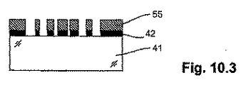
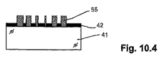
図10.1では、ここでもまた、プレート41上に調製された微細構造化金属マスク42が示され、今回は、図10.2で見てとれるように、フォトレジスト層55でコーティングされる。微細構造化金属マスクを上に有する基材の背面からUV暴露を実施する。
FIG. 10.1 again shows a
次のステップで、微細構造化フォトレジストが生じるようなフォトレジスト現像を実施した。この場合にも、フォトリソグラフィープロセスのためにポジ又はネガフォトレジストを使用することもできる。図10.3は、得られた微細構造化フォトレジスト層55をポジレジストとともに示し、図10.4は、得られた微細構造化フォトレジスト層55をネガレジストとともに示す。
In the next step, photoresist development was performed to produce a microstructured photoresist. Again, a positive or negative photoresist can be used for the photolithography process. FIG. 10.3 shows the resulting
実施例4
図11.1及び11.2を参照して、本発明の光学的に有効な表面レリーフ微細構造を有する表面区域を有する要素を製造するさらなる方法を説明する。
Example 4
With reference to FIGS. 11.1 and 11.2, a further method of manufacturing an element having a surface area with an optically effective surface relief microstructure of the present invention will be described.
基材として、ガラスプレート59をエッチング性材料、たとえば架橋性プレポリマーの層60でコーティングする。あるいはまた、ポリマー基材、たとえばプレキシグラスをさらなるコーティングなしで直接使用することもできる。
As a substrate, a
次いで、実施例1に記載した方法にしたがって、基材の上に微細構造化金属マスク61を生成する(図11.1)。
Then, according to the method described in Example 1, a
次のステップで、装置を、プラズマイオンが金属マスクの穴を貫通するようなドライエッチングに付した。酸素が適当なプラズマエッチング媒体である。ポリマー及び金属のエッチング選択性は非常に高い。したがって、ナノメートル厚さの金属ゾーンでさえ酸素プラズマによって攻撃され、微細又はナノ溝を生成することができる。プラズマエッチングの期間が下部領域の深さ、ひいては最終的な色外観を決定する。ガラスが基材として選択されるならば、ガラスは、エッチングの停止材料として働くこともできる。 In the next step, the apparatus was subjected to dry etching such that plasma ions penetrated the holes in the metal mask. Oxygen is a suitable plasma etching medium. The etch selectivity of polymers and metals is very high. Thus, even nanometer-thick metal zones can be attacked by oxygen plasma to produce fine or nanogrooves. The duration of the plasma etch determines the depth of the lower region and thus the final color appearance. If glass is selected as the substrate, it can also serve as an etch stop material.
最後に、適当なウェットエッチング溶液を用いるウェットエッチングによって金属マスクを除去する。 Finally, the metal mask is removed by wet etching using a suitable wet etching solution.
実施例5
前述のように、本発明の光学的に有効な表面レリーフ微細構造を有する表面区域を有する要素は、複製技術のためのマスタとして使用することができる。たとえば、実施例1〜4の方法にしたがって調製された要素が適当である。調製後、マスタの表面にある残留金属ゾーンを取り除くために、要素を短期間ウェットエッチング浴に暴露することができる。
Example 5
As mentioned above, elements having surface areas with optically effective surface relief microstructures of the present invention can be used as masters for replication technology. For example, elements prepared according to the methods of Examples 1-4 are suitable. After preparation, the element can be briefly exposed to a wet etch bath to remove residual metal zones on the surface of the master.
すると、微細構造化マスタは、金属シムの生成のために準備ができる。これは、薄い出発金属層、たとえば金、銀などを被着させたのち、ニッケルをガルバニック被着させることによって実施される。そして、このニッケルシムを使用して、適当な薄膜ポリマー材料への熱間エンボス加工によって、又は適当なUV硬化性材料へのUV注型成形によって複製を製造する。 The microstructured master is then ready for metal shim generation. This is done by depositing a thin starting metal layer, such as gold, silver, etc., followed by galvanic deposition of nickel. This nickel shim is then used to make a replica by hot embossing into a suitable thin film polymer material or by UV casting into a suitable UV curable material.
さらには、微細構造化複製物をアルミニウム又は類似金属で金属コーティングして良好な反射面を製造することができる。これは、特に、複製物が安全保障装置として適用される場合に当てはまる。 Furthermore, the microstructured replica can be metal coated with aluminum or a similar metal to produce a good reflective surface. This is especially true when the replica is applied as a security device.
最後に、装置を誘電性パシベーション膜で保護することもできるし、後で製品に適用するのに適した接着剤で直接コーティングすることもできる。このようにして、微細構造の表面変調を誘電体で埋める。 Finally, the device can be protected with a dielectric passivation film or coated directly with an adhesive suitable for later application to the product. In this way, the surface modulation of the microstructure is filled with the dielectric.
上記方法に基づく反射装置は基本的にモノクローム反射を示す。調製に依存して、試料を傾けたときに色の変化が認められることもある。しかし、これらの装置の一つの特徴は、虹色が認められないこと及び、したがって、標準的なホログラムとは有意に異なるということである。 A reflection device based on the above method basically exhibits monochrome reflection. Depending on the preparation, a color change may be observed when the sample is tilted. However, one feature of these devices is that no iridescence is seen and, therefore, significantly different from standard holograms.
実施例6
また、異なる表面レリーフ微細構造を有する二つ以上の区域を一つの要素に合わせる又は混合することが当然可能である。このより複雑なタイプの要素は、たとえばマルチカラーイメージを生成することを可能にし、それらの複雑さのおかげで、より高いレベルの安全保障を有することができる。
Example 6
It is of course possible to combine or mix two or more zones having different surface relief microstructures into one element. This more complex type of element makes it possible, for example, to generate multi-color images, and thanks to their complexity, can have a higher level of security.
図12.1〜12.4には、本発明の異なる表面レリーフ微細構造を有する二つの区域を有する要素を製造する方法の例が概説されている。 FIGS. 12.1 to 12.4 outline an example of a method for manufacturing an element having two zones with different surface relief microstructures of the present invention.
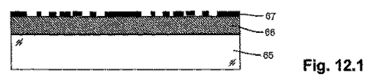
ガラス又はプラスチックのプレート65及びエッチング性材料の層66を含む基材に対し、上記プロセスステップにしたがって微細構造化金属膜67をコーティングする(図12.1)。ここでもまた、適当なポリマーコーティングを有するガラスもしくはプラスチックプレート又はポリマープレート、たとえばPPMA(プレキシグラス)を使用することができる。
A substrate comprising a glass or
次に、調製した基材の表面に1回目のプラズマエッチングを適用する。エッチング深さが最初の最終的に出現する色を決定する(図12.2)。 Next, the first plasma etching is applied to the surface of the prepared substrate. The first final appearing color of the etch depth is determined (FIG. 12.2).
次に、ここまで生成した表面レリーフ微細構造をポジフォトレジストの層68でコーティングし、特定区域69をUV光に暴露する。フォトレジストを現像することにより、区域69中の露光したレジスト材料を洗い流す(図12.3)。
Next, the surface relief microstructure produced thus far is coated with a
ここで、区域68中にすでに存在する微細構造を第二のエッチングステップでさらにエッチングすることができる(図12.4)。さらなるエッチングステップは深さを増し、区域68中の微細構造の色を決定する。その結果、異なる光学的に有効な表面レリーフ微細構造を有する二つの区域69及び70を有する要素が提供される。
Here, the microstructure already present in the
望むならば、一部の区域をカバーし、残りの露呈区域をエッチングする前記ステップを繰り返して、異なる微細構造を有する三つ以上の区域を提供することもできる。 If desired, the above steps of covering some areas and etching the remaining exposed areas can be repeated to provide more than two areas having different microstructures.
使用されるマスクは、10マイクロメートルを優に下回る画素サイズを保持する非常に高い解像度で達成することができる。したがって、色及び画素配設の適当な選択が、加法混色に基づくイメージの生成をも可能にする。 The mask used can be achieved with very high resolution, retaining a pixel size well below 10 micrometers. Thus, the proper choice of color and pixel arrangement also enables the generation of images based on additive color mixing.
実施例7
本発明の表面レリーフ微細構造はまた、反射性又は部分反射性にすることもできる。対応する実施例が図13.1及び13.2に示されている。
Example 7
The surface relief microstructure of the present invention can also be reflective or partially reflective. Corresponding embodiments are shown in FIGS. 13.1 and 13.2.
一般に、強い色反射のためには、微細構造を反射性材料、たとえばアルミニウム、金、クロム、銅などの薄い層71でコーティングする。そのような膜71の厚さが、高反射性又は部分反射性の装置を得ることができるような反射及び透過の程度を決定する。
In general, for strong color reflection, the microstructure is coated with a
層71のために部分反射性の金属膜を使用する代わりに、高又は低屈折率コーティングを使用することもできる。高屈折率材料の例はZnS、ZnSe、ITO又はITO2である。また、高屈折率材料のナノ粒子を含む複合材料が適当であるかもしれない。
Instead of using a partially reflective metal film for
あるいはまた、微細構造を高反射性材料で部分的にコーティングすることにより、たとえばはじめに微細構造全体をコーティングし、次にコーティングを部分的に除去して微細構造全体の一部だけが反射性材料で覆われるようにすることにより、部分反射性装置を得ることもできる。これは、反射性材料の層71’が特定の部分72で途切れている図13.2に示されている。
Alternatively, by partially coating the microstructure with a highly reflective material, for example, first coating the entire microstructure and then partially removing the coating so that only a portion of the entire microstructure is the reflective material. By making it cover, a partially reflective device can also be obtained. This is illustrated in FIG. 13.2 where the layer of
また、図13.1及び13.2には、装置の色出現をさらに高めるために、たとえば、特定の吸収挙動を有する透明な誘電体である保護及びパシベーション膜73が示されている。
In order to further enhance the color appearance of the device, FIGS. 13.1 and 13.2 show, for example, a protective and
実施例8
本発明の表面レリーフ微細構造の光学挙動を実証するために、図14.1及び14.2に、例示的な要素の反射スペクトルが示されている。要素は、実施例4の方法(微細構造化金属マスクのエッチング)にしたがって、約20ナノメートルの最終的な薄膜アルミニウムコーティングを含めて製造し、約1.5の屈折率の透明なパシベーション膜を介して計測した。
Example 8
In order to demonstrate the optical behavior of the surface relief microstructure of the present invention, the reflection spectra of exemplary elements are shown in FIGS. 14.1 and 14.2. The element was fabricated according to the method of Example 4 (etching of the microstructured metal mask), including a final thin film aluminum coating of about 20 nanometers, and a transparent passivation film with a refractive index of about 1.5 was produced. Measured through.
光学挙動は、この場合は緑である要素の散乱性非正反射色をもっとも明確な特徴とする。 The optical behavior is most clearly characterized by the scattering non-specular color of the element which in this case is green.
様々な照射角及び検出器角で反射スペクトルを測定することにより、製造した様々な例示的な要素を特性決定した。使用した分光光度計は、Perkin Elmer Lambda 900であり、調節可能な試料角及び調節可能な検出器角で反射スペクトルを計測することを可能にするPela 1030オプションを装備したものであった。300〜800ナノメートルの波長範囲で典型的な反射スペクトルを計測した。記載した計測のために特別な偏光装備は使用しなかった。鏡面反射ジオメトリ(入力角=出力角又は検出器角=試料角×2)の場合に相当する上述の正反射の場合に例外的な照射及び検出器条件が存在する。 Various exemplary elements produced were characterized by measuring reflection spectra at various illumination and detector angles. The spectrophotometer used was a Perkin Elmer Lambda 900, equipped with a Pela 1030 option that allows measuring the reflection spectrum with an adjustable sample angle and an adjustable detector angle. A typical reflection spectrum was measured in the wavelength range of 300-800 nanometers. No special polarization equipment was used for the measurements described. There are exceptional illumination and detector conditions in the case of specular reflection described above, which corresponds to the case of specular reflection geometry (input angle = output angle or detector angle = sample angle × 2).
例示的な要素の反射スペクトルが図14.1に示されている。照射角又は試料角SAは30°である。この角度は、図中左上の挿絵で示すように、基材表面から照射垂直面までの角度の逸脱である。検出器角DAは、同じく左上の挿絵で示すように、照射方向と検出器方向との間の角度である。 The reflection spectrum of an exemplary element is shown in Figure 14.1. The irradiation angle or sample angle SA is 30 °. This angle is the deviation of the angle from the substrate surface to the irradiation vertical plane, as shown in the upper left illustration in the figure. The detector angle DA is an angle between the irradiation direction and the detector direction as shown in the upper left illustration.
反射スペクトルは、525ナノメートルでの強い反射最大値、350ナノメートルでのもう一つの最大値及び400ナノメートルでの最小値を示す。これらの顕著な最大値及び最小値が、反射光の良好な色飽和の原因である。最大反射は、正反射から20°ずれている40°の検出器角で達成されている。30°及び50°の検出器角の場合、反射光輝度の低下が見られ、この場合、それに伴う波長シフトはあまり大きくない。 The reflection spectrum shows a strong reflection maximum at 525 nanometers, another maximum at 350 nanometers and a minimum at 400 nanometers. These remarkable maximum and minimum values are responsible for the good color saturation of the reflected light. Maximum reflection is achieved with a detector angle of 40 °, which is 20 ° off of specular reflection. For detector angles of 30 ° and 50 °, a decrease in reflected light brightness is seen, and the associated wavelength shift is not very large.
正反射光は非正反射光とは異なる。正反射は飽和マゼンタ色に見える。対応する反射スペクトルが図14.2に示されている。正反射計測の場合、検出器角DAは試料角SAの2倍である。ここでもまた、図14.1で見られる散乱反射の相補スペクトルにほぼ対応する顕著な変調がチャート中に見られる。これは、発生している散乱の最大部分が図14.1の計測で得られているということに注目することによって理解することができる。主要な色感応性散乱又は吸収チャネルが存在しないならば、正反射に関する相補スペクトルが残される。約4%のバックグラウンドが、本ケースではガラスである装置の保護用パシベーション層における無色性反射に対応する。また、図14.2に見てとれるように、正反射光の色スペクトルは装置の傾動に対して非常に非感応性である。 Regular reflection light is different from non-specular reflection light. Regular reflections appear saturated magenta. The corresponding reflection spectrum is shown in Fig. 14.2. In the case of specular reflection measurement, the detector angle DA is twice the sample angle SA. Again, there is a noticeable modulation in the chart that roughly corresponds to the complementary spectrum of scattered reflection seen in FIG. 14.1. This can be understood by noting that the largest portion of the scattering that has occurred is obtained in the measurement of FIG. 14.1. If there is no primary color sensitive scattering or absorption channel, a complementary spectrum for specular reflection is left. About 4% of the background corresponds to colorless reflections in the protective passivation layer of the device, which in this case is glass. Also, as can be seen in FIG. 14.2, the color spectrum of specularly reflected light is very insensitive to device tilt.
実施例9
図15.1及び15.2は、本発明の要素のもう一つの例の反射スペクトルを示す。要素は、実施例4の方法にしたがって製造した。その散乱色はオレンジである。
Example 9
Figures 15.1 and 15.2 show the reflection spectra of another example of an element of the invention. The element was manufactured according to the method of Example 4. Its scattering color is orange.
図15.1を参照すると、照射角又は試料角SAは30°である。反射スペクトルは、583ナノメートルでの強い反射最大値、380ナノメートルでのもう一つの最大値及び453ナノメートルでの最小値を示す。これらの最大値及び最小値が明るいオレンジ色の反射光の原因である。最大反射は、正反射から20°ずれている40°の検出器角DAで達成されている。50°の検出器角の場合、反射光輝度の低下が認められ、それに伴う波長シフトは約30ナノメートルである。 Referring to FIG. 15.1, the irradiation angle or sample angle SA is 30 °. The reflection spectrum shows a strong reflection maximum at 583 nanometers, another maximum at 380 nanometers and a minimum at 453 nanometers. These maximum and minimum values are responsible for the bright orange reflected light. Maximum reflection is achieved with a detector angle DA of 40 °, which is 20 ° off of specular reflection. For a detector angle of 50 °, a decrease in reflected light intensity is observed, with a corresponding wavelength shift of about 30 nanometers.
同じ例示的な要素の正反射が図15.2に示されている。ここでもまた、図15.1で見られる散乱反射の相補スペクトルにほぼ対応する顕著な変調が見られる。しかし、586ナノメートルでの最小値はあまり顕著ではなく、反射光の飽和度があまり高くないことを意味している。視認される装置色は不飽和青である。 The specular reflection of the same exemplary element is shown in Figure 15.2. Again, there is a noticeable modulation approximately corresponding to the complementary spectrum of scattered reflection seen in FIG. 15.1. However, the minimum value at 586 nanometers is not so noticeable, meaning that the saturation of the reflected light is not very high. The device color visually recognized is unsaturated blue.
Claims (20)
異なる透明度の第一及び第二のゾーンの微細構造を有し、マスクの第一の方向において、第一のゾーンから第二のゾーンまで又はその逆に各20マイクロメートル以内に平均で一つ以上の移行部があり、第一の方向に対して垂直であるマスクの第二の方向において、第一のゾーンから第二のゾーンまで又はその逆に各200マイクロメートル以内に平均で一つ以上の移行部があり、第一の方向において移行部の配設が非周期性であるマスクを創製することと、
マスクを用いて、樹脂又はレジスト(49、55、60、66)の表面にレリーフ微細構造を生成して、マスクの第一のゾーンに対応する上部領域(13)及びマスクの第二のゾーンに対応する下部領域(14)を製造し、レリーフ変調深さが表面区域全体で等しくなるよう、上部領域(13)が上部レリーフ平坦域(15、51)に位置し、下部領域(14)が下部レリーフ平坦域(16、52)に位置するようにすること
を含む方法。 A method of manufacturing an element having at least one surface area having a surface relief microstructure for use in a security device comprising:
Has a first and a fine pore structure of the second zone of different transparency, one in a first direction of the mask, on average within the 20 micrometer from the first zone to the second zone up or vice versa In the second direction of the mask that has the above transitions and is perpendicular to the first direction , one or more on average within 200 micrometers from the first zone to the second zone or vice versa There are transition, and that the arrangement of the transition portion in a first direction to create a mask which is non-periodic,
Using the mask, a relief microstructure is created on the surface of the resin or resist (49, 55, 60, 66) to form the upper region (13) corresponding to the first zone of the mask and the second zone of the mask. The corresponding lower region (14) is manufactured and the upper region (13) is located in the upper relief flat region (15, 51) and the lower region (14) is lower so that the relief modulation depth is equal over the entire surface area. Locating in the relief plateau (16, 52).
波形面構造を有する膜(43)をマスク材料の層(42)に被着させ、
波形面の下ゾーンの膜の材料が除去され、下にあるマスク材料の一部(44)が露呈するまで膜(43)の厚さを減らし、
マスクの露呈された一部(44)を除去する
ことによって創製される、請求項1記載の方法。 The microstructure of the first and second zones of different transparency of the mask is
Depositing a film (43) having a corrugated surface structure on a layer (42) of mask material;
Reduce the thickness of the film (43) until the material of the film in the lower zone of the corrugated surface is removed and a portion of the underlying mask material (44) is exposed,
The method of claim 1, wherein the method is created by removing an exposed portion (44) of the mask.
表面レリーフ微細構造が上部領域(13)から下部領域(14)まで及び下部領域(14)から上部領域(13)までの移行部の表面変調を有し、
少なくとも表面区域の第一の方向において、上部領域(13)から下部領域(14)まで又はその逆に各20マイクロメートル以内に少なくとも一つの移行部があり、第一の方向に対して垂直である前記表面区域の第二の方向において、上部領域から下部領域まで又はその逆に各200マイクロメートル以内に平均で一つ以上の移行部があることを特徴とし、
(i)少なくとも第一の方向において移行部の配設が非周期性であり、
(ii)レリーフ変調深さが表面区域全体で等しくなるよう、上部領域(13)が上部レリーフ平坦域(15、51)に位置し、下部領域が下部レリーフ平坦域(16、52)に位置することを特徴とする要素。 An element having at least one surface area with a surface relief microstructure (12) for use in a security device,
The surface relief microstructure has surface modulation at the transition from the upper region (13) to the lower region (14) and from the lower region (14) to the upper region (13);
There is at least one transition within each 20 micrometers from the upper region (13) to the lower region (14) or vice versa, at least in the first direction of the surface area, and perpendicular to the first direction In the second direction of the surface area, there is an average of one or more transitions within 200 micrometers each from the upper region to the lower region or vice versa,
(I) an at least a first direction arranged in the transition portion is non-periodic,
(Ii) the relief modulation depth is to be equal in the entire surface area, the upper region (13) is located above the relief plateau (15 and 51), a lower region located below the relief plateau (16, 52) An element characterized by that.
(式中、△x1は、全ピーク高さの高さ1/eのところで計測した第一のピークの幅であり、△x2は、全ピーク高さの高さ1/eのところで計測した第二のピークの幅であり、dは二つのピークの距離である)
を規定することができ、メリット関数Mが2よりも大きいことを特徴とする、請求項4〜8のいずれか1項記載の要素。 The height histogram of the surface relief microstructure has the first and second prominent peaks, the merit function
(Where Δx 1 is the width of the first peak measured at height 1 / e of the total peak height, and Δx 2 is measured at height 1 / e of the total peak height. The width of the second peak and d is the distance between the two peaks)
9. The element according to claim 4, wherein the merit function M is larger than 2. 9.
Applications Claiming Priority (3)
| Application Number | Priority Date | Filing Date | Title |
|---|---|---|---|
| EP06113901.0 | 2006-05-12 | ||
| EP06113901A EP1855127A1 (en) | 2006-05-12 | 2006-05-12 | Optically effective surface relief microstructures and method of making them |
| PCT/CH2007/000227 WO2007131375A1 (en) | 2006-05-12 | 2007-05-07 | Optically effective surface relief microstructures and method of making them |
Publications (3)
| Publication Number | Publication Date |
|---|---|
| JP2009536883A JP2009536883A (en) | 2009-10-22 |
| JP2009536883A5 JP2009536883A5 (en) | 2010-06-17 |
| JP5570210B2 true JP5570210B2 (en) | 2014-08-13 |
Family
ID=36997641
Family Applications (1)
| Application Number | Title | Priority Date | Filing Date |
|---|---|---|---|
| JP2009508082A Active JP5570210B2 (en) | 2006-05-12 | 2007-05-07 | Optically effective surface relief microstructure and manufacturing method thereof |
Country Status (9)
| Country | Link |
|---|---|
| US (2) | US8840146B2 (en) |
| EP (4) | EP1855127A1 (en) |
| JP (1) | JP5570210B2 (en) |
| CN (2) | CN101443681B (en) |
| BR (1) | BRPI0711415B1 (en) |
| ES (1) | ES2510515T3 (en) |
| RU (1) | RU2428724C2 (en) |
| TW (1) | TWI437276B (en) |
| WO (1) | WO2007131375A1 (en) |
Cited By (4)
| Publication number | Priority date | Publication date | Assignee | Title |
|---|---|---|---|---|
| WO2017119492A1 (en) | 2016-01-07 | 2017-07-13 | 凸版印刷株式会社 | Optical element and article equipped with optical element |
| WO2017191842A1 (en) | 2016-05-06 | 2017-11-09 | 凸版印刷株式会社 | Display body |
| EP3572852A1 (en) | 2015-10-19 | 2019-11-27 | Toppan Printing Co., Ltd. | Display, article with display, and method of observing display |
| US10908330B2 (en) | 2016-05-06 | 2021-02-02 | Toppan Printing Co., Ltd. | Display |
Families Citing this family (43)
| Publication number | Priority date | Publication date | Assignee | Title |
|---|---|---|---|---|
| EP1855127A1 (en) * | 2006-05-12 | 2007-11-14 | Rolic AG | Optically effective surface relief microstructures and method of making them |
| JP4961944B2 (en) | 2006-10-24 | 2012-06-27 | 凸版印刷株式会社 | Display and printed matter |
| DE102008005019B4 (en) | 2008-01-17 | 2010-08-05 | Ovd Kinegram Ag | Foil element and the use of this foil element |
| DE102008007620A1 (en) * | 2008-02-04 | 2009-08-27 | Hologram Industries Research Gmbh | Method for individualizing volume holograms and security elements produced therewith |
| WO2009125769A1 (en) * | 2008-04-08 | 2009-10-15 | 株式会社ニコン | Optical element, process for producing the optical element, and optical device |
| EP3040747B1 (en) * | 2008-04-18 | 2022-06-22 | Toppan Printing Co., Ltd. | Display and labeled article |
| RU2540092C2 (en) * | 2009-02-18 | 2015-01-27 | Ролик Аг | Embossed surface microstructures, devices and method for their making |
| EP2508922B2 (en) * | 2009-12-01 | 2023-08-16 | Toppan Printing Co., Ltd. | Display body and labeled article |
| EP2585862B8 (en) | 2010-06-25 | 2017-10-11 | Andrew Richard Parker | Optical effect structures |
| JP2012078447A (en) * | 2010-09-30 | 2012-04-19 | Toppan Printing Co Ltd | Display body and article with label |
| EP2441593B1 (en) | 2010-10-13 | 2020-04-15 | Hueck Folien Gesellschaft m.b.H. | Security element with achromatic features |
| CN102455592B (en) * | 2010-10-22 | 2013-12-04 | 比亚迪股份有限公司 | Preparation method of film |
| IT1402447B1 (en) * | 2010-11-10 | 2013-09-13 | Plasma Solution S R L | REALIZATION OF ANTI-COUNTERFEITING LABELS EQUIPPED WITH HIDDEN IDENTIFICATION GRAPHICS. |
| FR2968239B1 (en) * | 2010-12-07 | 2012-12-21 | Hologram Ind | SECURE PRODUCT AND METHOD OF MAKING SAID SECURE PRODUCT |
| DE102011014114B3 (en) * | 2011-03-15 | 2012-05-10 | Ovd Kinegram Ag | Multi-layer body and method for producing a multi-layer body |
| EP2699951B1 (en) | 2011-04-20 | 2022-06-22 | ROLIC Technologies AG | Asymmetric optically effective surface relief microstructures and method of making them |
| US9383648B2 (en) | 2011-11-14 | 2016-07-05 | Dai Nippon Printing Co., Ltd. | Anti-counterfeiting marker sheet and manufacturing method therefor, anti-counterfeiting function-imparting member, and article provided with anti-counterfeiting function |
| DE102011121588A1 (en) * | 2011-12-20 | 2013-06-20 | Giesecke & Devrient Gmbh | Security element for security papers, documents of value or the like |
| EP2635006B1 (en) * | 2012-03-02 | 2018-12-19 | LG Electronics, Inc. | Mobile terminal comprising an image module provided thereon |
| JP2013182269A (en) * | 2012-03-05 | 2013-09-12 | Oji Holdings Corp | Optical diffuser and light source unit |
| FR2989474B1 (en) * | 2012-04-13 | 2014-11-28 | Hologram Ind | OPTICAL SECURITY COMPONENT, MANUFACTURE OF SUCH A COMPONENT, AND SECURE PRODUCT EQUIPPED WITH SUCH A COMPONENT |
| DE102012105571B4 (en) * | 2012-06-26 | 2017-03-09 | Ovd Kinegram Ag | Decorative element as well as security document with a decorative element |
| US20140009838A1 (en) * | 2012-07-03 | 2014-01-09 | 3M Innovative Properties Company | Decorative film articles utilizing fresnel lens films |
| US9958580B2 (en) | 2012-11-29 | 2018-05-01 | Tomoegawa Co., Ltd. | Anisotropic optical film |
| US9939682B2 (en) * | 2013-02-15 | 2018-04-10 | E-Vision, Llc | Liquid crystal alignment layers and method of fabrication |
| WO2015172190A1 (en) * | 2014-05-16 | 2015-11-19 | Innovia Security Pty Ltd | Hybrid security device for security document or token |
| AT515845B1 (en) * | 2014-06-10 | 2017-05-15 | Hueck Folien Gmbh | Security element and method for producing a security element with light-scattering structures |
| EP3210069A4 (en) | 2014-10-24 | 2018-05-30 | Wavefront Technology, Inc. | Optical products, masters for fabricating optical products, and methods for manufacturing masters and optical products |
| AU2016240316B2 (en) * | 2015-03-31 | 2020-10-22 | Andrew Richard Parker | Optical effect structures |
| CN104766537A (en) * | 2015-04-15 | 2015-07-08 | 四川云盾光电科技有限公司 | Laser scattering image display method based on micro-nano structure |
| AU2016248847B2 (en) | 2015-04-16 | 2021-07-15 | Rolic Ag | Multiple image scattering device |
| US9751618B2 (en) * | 2015-05-06 | 2017-09-05 | The Boeing Company | Optical effects for aerodynamic microstructures |
| WO2017011476A1 (en) | 2015-07-13 | 2017-01-19 | Wavefront Technology, Inc. | Optical products, masters for fabricating optical products, and methods for manufacturing masters and optical products |
| MX2018001413A (en) | 2015-08-07 | 2018-04-13 | Rolic Tech Ag | Azimuthally modulated scattering device. |
| US11113919B2 (en) | 2017-10-20 | 2021-09-07 | Wavefront Technology, Inc. | Optical switch devices |
| US10850550B2 (en) | 2016-04-22 | 2020-12-01 | Wavefront Technology, Inc. | Optical switch devices |
| KR102566919B1 (en) | 2017-07-26 | 2023-08-14 | 도판 인사츠 가부시키가이샤 | Optical structure and authentication body |
| US10802185B2 (en) | 2017-08-16 | 2020-10-13 | Lumentum Operations Llc | Multi-level diffractive optical element thin film coating |
| US10712475B2 (en) | 2017-08-16 | 2020-07-14 | Lumentum Operations Llc | Multi-layer thin film stack for diffractive optical elements |
| CN107817541B (en) * | 2017-10-31 | 2019-09-17 | 武汉华星光电技术有限公司 | Resist the production method of dizzy cover board |
| WO2020214239A1 (en) | 2019-04-19 | 2020-10-22 | Wavefront Technology, Inc. | Optical switch devices |
| EP4067102A1 (en) | 2021-04-02 | 2022-10-05 | Kaunas University of Technology | An optical device with ordered scatterer arrays for secure identity and a method of producing the same |
| CN113866171B (en) * | 2021-12-02 | 2022-03-18 | 武汉飞恩微电子有限公司 | Circuit board dispensing detection method and device and computer readable storage medium |
Family Cites Families (29)
| Publication number | Priority date | Publication date | Assignee | Title |
|---|---|---|---|---|
| US4329410A (en) * | 1979-12-26 | 1982-05-11 | The Perkin-Elmer Corporation | Production of X-ray lithograph masks |
| US5084351A (en) * | 1979-12-28 | 1992-01-28 | Flex Products, Inc. | Optically variable multilayer thin film interference stack on flexible insoluble web |
| EP0525477B1 (en) | 1991-07-26 | 1998-09-16 | Rolic AG | Oriented photopolymers and process of preparing same |
| TW275109B (en) * | 1993-08-06 | 1996-05-01 | Commw Scient Ind Res Org | |
| EP0712012A1 (en) * | 1994-11-09 | 1996-05-15 | International Business Machines Corporation | Authentication label and authenticating pattern incorporating diffracting structure and method of fabricating them |
| US6162306A (en) * | 1997-11-04 | 2000-12-19 | Kawasaki Steel Corporation | Electromagnetic steel sheet having excellent high-frequency magnetic properities and method |
| DE19940389A1 (en) * | 1999-08-25 | 2001-03-01 | Wilex Biotechnology Gmbh | Selective inhibitors of the urokinase plasminogen activator |
| DE60040011D1 (en) * | 1999-10-19 | 2008-10-02 | Rolic Ag | TOPOLOGICALLY STRUCTURED POLYMER COATING |
| JP3391763B2 (en) * | 2000-03-03 | 2003-03-31 | 沖電気工業株式会社 | Manufacturing method of mask |
| US6322938B1 (en) * | 2000-05-22 | 2001-11-27 | The United States Of America As Represented By The Secretary Of The Air Force | Nanolithography for multi-passband grating filters |
| WO2002010804A1 (en) * | 2000-07-31 | 2002-02-07 | Rochester Photonics Corporation | Structure screens for controlled spreading of light |
| US6686042B1 (en) | 2000-09-22 | 2004-02-03 | Flex Products, Inc. | Optically variable pigments and foils with enhanced color shifting properties |
| US6686027B1 (en) * | 2000-09-25 | 2004-02-03 | Agra Vadeko Inc. | Security substrate for documents of value |
| JP3753673B2 (en) * | 2001-06-20 | 2006-03-08 | セイコーエプソン株式会社 | Manufacturing method of liquid crystal display device |
| US6510200B1 (en) * | 2001-06-29 | 2003-01-21 | Osmic, Inc. | Multi-layer structure with variable bandpass for monochromatization and spectroscopy |
| US6855408B2 (en) * | 2002-01-25 | 2005-02-15 | Showa Denko K.K. | Composite metal material and method for manufacturing the same, etched metal material and method for manufacturing the same and electrolytic capacitor |
| KR100501247B1 (en) * | 2002-04-17 | 2005-07-18 | 광주과학기술원 | Etching mask using azobenzene compounds |
| EP1400838A1 (en) * | 2002-09-19 | 2004-03-24 | Rolic AG | Thin films with corrugated surface topologies and method to produce them |
| US6902871B2 (en) * | 2002-10-03 | 2005-06-07 | Lumera Corporation | Method for manufacturing polymer microstructures and polymer waveguides |
| US6958207B1 (en) * | 2002-12-07 | 2005-10-25 | Niyaz Khusnatdinov | Method for producing large area antireflective microtextured surfaces |
| EP1649319A1 (en) * | 2003-07-17 | 2006-04-26 | Koninklijke Philips Electronics N.V. | Method of manufacturing a reflector, and liquid crystal display device including such a reflector |
| US7252869B2 (en) * | 2003-10-30 | 2007-08-07 | Niyaz Khusnatdinov | Microtextured antireflective surfaces with reduced diffraction intensity |
| DE102004003984A1 (en) * | 2004-01-26 | 2005-08-11 | Giesecke & Devrient Gmbh | Lattice image with one or more grid fields |
| JP2005215642A (en) * | 2004-02-02 | 2005-08-11 | Shin Sti Technology Kk | Photomask and method for manufacturing diffusion reflector |
| JP4649222B2 (en) * | 2004-03-31 | 2011-03-09 | キヤノン株式会社 | Manufacturing method of imaging lens |
| US7268948B2 (en) * | 2004-03-31 | 2007-09-11 | Canon Kabushiki Kaisha | Optical element and optical scanning device using the same |
| US6979521B1 (en) * | 2004-06-29 | 2005-12-27 | Matsushita Electric Industrial Co., Ltd. | Method of making grayscale mask for grayscale DOE production by using an absorber layer |
| WO2006007742A1 (en) | 2004-07-21 | 2006-01-26 | Rolic Ag | Anisotropic optical devices and method for making same |
| EP1855127A1 (en) * | 2006-05-12 | 2007-11-14 | Rolic AG | Optically effective surface relief microstructures and method of making them |
-
2006
- 2006-05-12 EP EP06113901A patent/EP1855127A1/en not_active Withdrawn
-
2007
- 2007-05-07 EP EP18157639.8A patent/EP3355087A1/en active Pending
- 2007-05-07 US US12/297,126 patent/US8840146B2/en active Active
- 2007-05-07 JP JP2009508082A patent/JP5570210B2/en active Active
- 2007-05-07 CN CN2007800173263A patent/CN101443681B/en active Active
- 2007-05-07 EP EP12191370.1A patent/EP2565686B1/en active Active
- 2007-05-07 EP EP07720124.2A patent/EP2021837B1/en not_active Revoked
- 2007-05-07 WO PCT/CH2007/000227 patent/WO2007131375A1/en active Application Filing
- 2007-05-07 BR BRPI0711415A patent/BRPI0711415B1/en not_active IP Right Cessation
- 2007-05-07 ES ES07720124.2T patent/ES2510515T3/en active Active
- 2007-05-07 RU RU2008148828/28A patent/RU2428724C2/en active
- 2007-05-07 CN CN201110362663.4A patent/CN102495525B/en active Active
- 2007-05-11 TW TW096116736A patent/TWI437276B/en not_active IP Right Cessation
-
2013
- 2013-12-17 US US14/108,453 patent/US10350843B2/en active Active
Cited By (7)
| Publication number | Priority date | Publication date | Assignee | Title |
|---|---|---|---|---|
| EP3572852A1 (en) | 2015-10-19 | 2019-11-27 | Toppan Printing Co., Ltd. | Display, article with display, and method of observing display |
| EP3816681A1 (en) | 2015-10-19 | 2021-05-05 | Toppan Printing Co., Ltd. | Display, article with display, and method of observing display |
| US11427025B2 (en) | 2015-10-19 | 2022-08-30 | Toppan Printing Co., Ltd. | Display, article with display, and method of observing display |
| WO2017119492A1 (en) | 2016-01-07 | 2017-07-13 | 凸版印刷株式会社 | Optical element and article equipped with optical element |
| US10921500B2 (en) | 2016-01-07 | 2021-02-16 | Toppan Printing Co., Ltd. | Optical element, and optical element-equipped article |
| WO2017191842A1 (en) | 2016-05-06 | 2017-11-09 | 凸版印刷株式会社 | Display body |
| US10908330B2 (en) | 2016-05-06 | 2021-02-02 | Toppan Printing Co., Ltd. | Display |
Also Published As
| Publication number | Publication date |
|---|---|
| WO2007131375A1 (en) | 2007-11-22 |
| TW200745620A (en) | 2007-12-16 |
| TWI437276B (en) | 2014-05-11 |
| JP2009536883A (en) | 2009-10-22 |
| CN102495525A (en) | 2012-06-13 |
| RU2008148828A (en) | 2010-08-10 |
| CN102495525B (en) | 2015-09-09 |
| EP2021837B1 (en) | 2014-07-09 |
| US20140106091A1 (en) | 2014-04-17 |
| EP2021837A1 (en) | 2009-02-11 |
| EP2565686B1 (en) | 2018-04-04 |
| EP3355087A1 (en) | 2018-08-01 |
| CN101443681B (en) | 2012-01-11 |
| BRPI0711415B1 (en) | 2019-01-02 |
| EP1855127A1 (en) | 2007-11-14 |
| US8840146B2 (en) | 2014-09-23 |
| US10350843B2 (en) | 2019-07-16 |
| RU2428724C2 (en) | 2011-09-10 |
| BRPI0711415A2 (en) | 2011-11-01 |
| CN101443681A (en) | 2009-05-27 |
| EP2565686A1 (en) | 2013-03-06 |
| US20090179418A1 (en) | 2009-07-16 |
| ES2510515T3 (en) | 2014-10-21 |
Similar Documents
| Publication | Publication Date | Title |
|---|---|---|
| JP5570210B2 (en) | Optically effective surface relief microstructure and manufacturing method thereof | |
| RU2540092C2 (en) | Embossed surface microstructures, devices and method for their making | |
| US11054551B2 (en) | Multiple image scattering device | |
| US11921303B2 (en) | Azimuthally modulated scattering device | |
| EP2699951B1 (en) | Asymmetric optically effective surface relief microstructures and method of making them |
Legal Events
| Date | Code | Title | Description |
|---|---|---|---|
| A521 | Request for written amendment filed |
Free format text: JAPANESE INTERMEDIATE CODE: A523 Effective date: 20100420 |
|
| A621 | Written request for application examination |
Free format text: JAPANESE INTERMEDIATE CODE: A621 Effective date: 20100420 |
|
| A131 | Notification of reasons for refusal |
Free format text: JAPANESE INTERMEDIATE CODE: A131 Effective date: 20120925 |
|
| A601 | Written request for extension of time |
Free format text: JAPANESE INTERMEDIATE CODE: A601 Effective date: 20121221 |
|
| A602 | Written permission of extension of time |
Free format text: JAPANESE INTERMEDIATE CODE: A602 Effective date: 20130104 |
|
| A521 | Request for written amendment filed |
Free format text: JAPANESE INTERMEDIATE CODE: A523 Effective date: 20130312 |
|
| RD13 | Notification of appointment of power of sub attorney |
Free format text: JAPANESE INTERMEDIATE CODE: A7433 Effective date: 20130902 |
|
| A521 | Request for written amendment filed |
Free format text: JAPANESE INTERMEDIATE CODE: A821 Effective date: 20130902 |
|
| A131 | Notification of reasons for refusal |
Free format text: JAPANESE INTERMEDIATE CODE: A131 Effective date: 20131008 |
|
| A521 | Request for written amendment filed |
Free format text: JAPANESE INTERMEDIATE CODE: A523 Effective date: 20131209 |
|
| TRDD | Decision of grant or rejection written | ||
| A01 | Written decision to grant a patent or to grant a registration (utility model) |
Free format text: JAPANESE INTERMEDIATE CODE: A01 Effective date: 20140617 |
|
| A61 | First payment of annual fees (during grant procedure) |
Free format text: JAPANESE INTERMEDIATE CODE: A61 Effective date: 20140624 |
|
| R150 | Certificate of patent or registration of utility model |
Ref document number: 5570210 Country of ref document: JP Free format text: JAPANESE INTERMEDIATE CODE: R150 |
|
| R250 | Receipt of annual fees |
Free format text: JAPANESE INTERMEDIATE CODE: R250 |
|
| R250 | Receipt of annual fees |
Free format text: JAPANESE INTERMEDIATE CODE: R250 |
|
| R250 | Receipt of annual fees |
Free format text: JAPANESE INTERMEDIATE CODE: R250 |
|
| R250 | Receipt of annual fees |
Free format text: JAPANESE INTERMEDIATE CODE: R250 |
|
| R250 | Receipt of annual fees |
Free format text: JAPANESE INTERMEDIATE CODE: R250 |
|
| R250 | Receipt of annual fees |
Free format text: JAPANESE INTERMEDIATE CODE: R250 |
|
| R250 | Receipt of annual fees |
Free format text: JAPANESE INTERMEDIATE CODE: R250 |