JP5558801B2 - Solid-state imaging device - Google Patents
Solid-state imaging device Download PDFInfo
- Publication number
- JP5558801B2 JP5558801B2 JP2009288459A JP2009288459A JP5558801B2 JP 5558801 B2 JP5558801 B2 JP 5558801B2 JP 2009288459 A JP2009288459 A JP 2009288459A JP 2009288459 A JP2009288459 A JP 2009288459A JP 5558801 B2 JP5558801 B2 JP 5558801B2
- Authority
- JP
- Japan
- Prior art keywords
- semiconductor substrate
- electrical connection
- pixel region
- disposed
- imaging device
- Prior art date
- Legal status (The legal status is an assumption and is not a legal conclusion. Google has not performed a legal analysis and makes no representation as to the accuracy of the status listed.)
- Expired - Fee Related
Links
- 238000003384 imaging method Methods 0.000 title claims description 25
- 239000004065 semiconductor Substances 0.000 claims description 86
- 239000000758 substrate Substances 0.000 claims description 74
- 238000006243 chemical reaction Methods 0.000 claims description 42
- 230000003321 amplification Effects 0.000 claims description 33
- 238000003199 nucleic acid amplification method Methods 0.000 claims description 33
- 238000012546 transfer Methods 0.000 claims description 29
- 238000009792 diffusion process Methods 0.000 claims description 14
- 238000010586 diagram Methods 0.000 description 7
- 230000002093 peripheral effect Effects 0.000 description 6
- 229910021420 polycrystalline silicon Inorganic materials 0.000 description 5
- 229920005591 polysilicon Polymers 0.000 description 5
- 230000035945 sensitivity Effects 0.000 description 5
- 238000012545 processing Methods 0.000 description 4
- 238000002955 isolation Methods 0.000 description 2
- 230000003071 parasitic effect Effects 0.000 description 2
- 238000013459 approach Methods 0.000 description 1
- 230000000052 comparative effect Effects 0.000 description 1
- 230000007423 decrease Effects 0.000 description 1
- 230000003247 decreasing effect Effects 0.000 description 1
- 230000007547 defect Effects 0.000 description 1
- 239000011159 matrix material Substances 0.000 description 1
- 238000000034 method Methods 0.000 description 1
- 238000012986 modification Methods 0.000 description 1
- 230000004048 modification Effects 0.000 description 1
- 239000007787 solid Substances 0.000 description 1
Images


Classifications
-
- H—ELECTRICITY
- H01—ELECTRIC ELEMENTS
- H01L—SEMICONDUCTOR DEVICES NOT COVERED BY CLASS H10
- H01L27/00—Devices consisting of a plurality of semiconductor or other solid-state components formed in or on a common substrate
- H01L27/14—Devices consisting of a plurality of semiconductor or other solid-state components formed in or on a common substrate including semiconductor components sensitive to infrared radiation, light, electromagnetic radiation of shorter wavelength or corpuscular radiation and specially adapted either for the conversion of the energy of such radiation into electrical energy or for the control of electrical energy by such radiation
- H01L27/144—Devices controlled by radiation
- H01L27/146—Imager structures
- H01L27/14601—Structural or functional details thereof
- H01L27/14609—Pixel-elements with integrated switching, control, storage or amplification elements
-
- H—ELECTRICITY
- H01—ELECTRIC ELEMENTS
- H01L—SEMICONDUCTOR DEVICES NOT COVERED BY CLASS H10
- H01L27/00—Devices consisting of a plurality of semiconductor or other solid-state components formed in or on a common substrate
- H01L27/14—Devices consisting of a plurality of semiconductor or other solid-state components formed in or on a common substrate including semiconductor components sensitive to infrared radiation, light, electromagnetic radiation of shorter wavelength or corpuscular radiation and specially adapted either for the conversion of the energy of such radiation into electrical energy or for the control of electrical energy by such radiation
- H01L27/144—Devices controlled by radiation
- H01L27/146—Imager structures
- H01L27/14643—Photodiode arrays; MOS imagers
- H01L27/14649—Infrared imagers
- H01L27/1465—Infrared imagers of the hybrid type
Landscapes
- Physics & Mathematics (AREA)
- Engineering & Computer Science (AREA)
- Power Engineering (AREA)
- Electromagnetism (AREA)
- Condensed Matter Physics & Semiconductors (AREA)
- General Physics & Mathematics (AREA)
- Computer Hardware Design (AREA)
- Microelectronics & Electronic Packaging (AREA)
- Solid State Image Pick-Up Elements (AREA)
- Transforming Light Signals Into Electric Signals (AREA)
Description
本発明は固体撮像装置に関し、具体的には、光電変換部と周辺回路部とを別基板に分けて構成した固体撮像装置に関する。 The present invention relates to a solid-state imaging device, and more specifically to a solid-state imaging device in which a photoelectric conversion unit and a peripheral circuit unit are configured on separate substrates.
固体撮像装置において、光電変換部と周辺回路部とを別基板に分けて形成し、それらをマイクロバンプ等で電気的に接続する構成が知られている。特許文献1には、垂直走査部、水平走査部等の光電変換部から信号を読みだすための周辺回路が、光電変換部が配された第1の半導体基板とは別の第2の半導体基板に配されている構成が開示されている。
In a solid-state imaging device, a configuration is known in which a photoelectric conversion unit and a peripheral circuit unit are formed separately on different substrates and are electrically connected by micro bumps or the like. In
より具体的には、第1の半導体基板には少なくとも光電変換部とフローティングディフュージョン(FD)と光電変換部の電荷をFDに転送する転送トランジスタとリセットトランジスタとが配されている。 More specifically, at least a photoelectric conversion unit, a floating diffusion (FD), a transfer transistor that transfers charges of the photoelectric conversion unit to the FD, and a reset transistor are arranged on the first semiconductor substrate.
一般に光電変換部は信号を取り出すための出力ノードと、基準電圧が供給されるノードとを有する。例えば光電変換部がフォトダイオードの場合には、カソードから信号を取り出し、アノードには基準電圧が供給されている。信号電荷として電子を用いる場合には、アノード側には接地電位が供給される。 In general, the photoelectric conversion unit has an output node for extracting a signal and a node to which a reference voltage is supplied. For example, when the photoelectric conversion unit is a photodiode, a signal is extracted from the cathode, and a reference voltage is supplied to the anode. When electrons are used as signal charges, a ground potential is supplied to the anode side.
特許文献1の図1には等価回路図としてフォトダイオードのアノードに接地電位が供給されている旨が記載されている。また図5には固体撮像装置の断面図が示されている。しかしながら特許文献1には、具体的にどのような方法で光電変換部に基準電圧を供給するかに関しては明示がない。
FIG. 1 of
本発明者らの検討によれば、光電変換部への基準電圧の供給の仕方によってはFDの容量を上昇させてしまい、画素の感度が低下してしまう場合があることがわかった。 According to the study by the present inventors, it has been found that the capacity of the FD is increased depending on how the reference voltage is supplied to the photoelectric conversion unit, and the sensitivity of the pixel may be decreased.
本発明は、上記課題に鑑み、光電変換部と周辺回路部とを別基板に分けて形成した場合の、好適な光電変換部への基準電圧を供給する構成を提供するものである。 In view of the above problems, the present invention provides a configuration for supplying a reference voltage to a suitable photoelectric conversion unit when the photoelectric conversion unit and the peripheral circuit unit are separately formed on different substrates.
本発明は上記課題に鑑み、光電変換部とフローティングディフュージョンと前記光電変換部の電荷を前記フローティングディフュージョンへ転送する転送トランジスタとが複数配された画素領域と前記複数のフローティングディフュージョンの各々に、リセット電位を供給する複数のリセットトランジスタと、前記複数のフローティングディフュージョンの各々の電位変化に基づく信号を増幅して出力する複数の増幅トランジスタと、前記光電変換部に基準電圧を供給するための基準電圧供給線と、を有し、前記画素領域及び前記基準電圧供給線が第1の半導体基板に配され、前記複数のリセットトランジスタもしくは前記複数の増幅トランジスタの少なくとも一方が第2の半導体基板に配された固体撮像装置であって、前記基準電圧供給線に電圧を供給するための電源線が前記第2の半導体基板に配されており、前記フローティングディフュージョンと、前記第2の半導体基板に配された前記リセットトランジスタ及び前記増幅トランジスタとを電気的に接続するための複数の第1の電気的接続部と、前記基準電圧供給線と前記電源線とを電気的に接続するための複数の第2の電気的接続部と、を有し、前記複数の第1の電気的接続部は、前記画素領域内に配され、前記複数の第2の電気的接続部は、前記画素領域外に配されていることを特徴とする。 In view of the above problems, the present invention provides a pixel region in which a plurality of photoelectric conversion units, floating diffusions, and transfer transistors that transfer charges of the photoelectric conversion units to the floating diffusions are arranged, and a reset potential in each of the plurality of floating diffusions. A plurality of reset transistors for supplying a reference voltage, a plurality of amplification transistors for amplifying and outputting a signal based on a change in potential of each of the plurality of floating diffusions, and a reference voltage supply line for supplying a reference voltage to the photoelectric conversion unit A solid state in which the pixel region and the reference voltage supply line are disposed on a first semiconductor substrate, and at least one of the plurality of reset transistors or the plurality of amplification transistors is disposed on a second semiconductor substrate. An imaging apparatus, wherein the reference voltage supply line A power supply line for supplying a voltage is disposed on the second semiconductor substrate, and electrically connects the floating diffusion to the reset transistor and the amplification transistor disposed on the second semiconductor substrate. A plurality of first electrical connections for connecting, and a plurality of second electrical connections for electrically connecting the reference voltage supply line and the power supply line. One electrical connection portion is disposed in the pixel region, and the plurality of second electrical connection portions are disposed outside the pixel region.
本発明によれば、光電変換部と周辺回路部とを別基板に分けた固体撮像装置において、フローティングディフュージョンの容量値を増加させることなく、光電変換部へ基準電圧を供給することが可能となる。 According to the present invention, in the solid-state imaging device in which the photoelectric conversion unit and the peripheral circuit unit are separated on different substrates, it is possible to supply the reference voltage to the photoelectric conversion unit without increasing the capacitance value of the floating diffusion. .
本発明の固体撮像装置の画素は、光電変換部、フローティングディフュージョン(FD)及び光電変換部の電荷をFDへ転送する転送トランジスタを含む。更に、FDの電位をリセット電位とするリセットトランジスタ、FDの電位変化に基づく信号を増幅(電荷増幅)して出力する増幅トランジスタを含む。 The pixel of the solid-state imaging device of the present invention includes a photoelectric conversion unit, a floating diffusion (FD), and a transfer transistor that transfers charges of the photoelectric conversion unit to the FD. Furthermore, a reset transistor having the potential of FD as a reset potential and an amplifying transistor for amplifying (charge amplification) and outputting a signal based on a change in the potential of FD are included.
光電変換部、FD、転送トランジスタが複数配された画素領域が第1の半導体基板に配されている。 A pixel region in which a plurality of photoelectric conversion units, FDs, and transfer transistors are arranged is arranged on the first semiconductor substrate.
そして複数の画素からの信号が出力される複数の共通出力線が第2の半導体基板に配されている。更に、画素よりも後段に設けられる読み出し回路及び画素からの信号を読み出すための走査回路を含む周辺回路部が第2の半導体基板に配されている。 A plurality of common output lines for outputting signals from the plurality of pixels are arranged on the second semiconductor substrate. Further, a peripheral circuit portion including a readout circuit provided at a stage subsequent to the pixel and a scanning circuit for reading out a signal from the pixel is provided on the second semiconductor substrate.
他の画素要素は第1の半導体基板もしくは第2の半導体基板のいずれかに配されていればよい。しかし、少なくともリセットトランジスタ、増幅トランジスタの少なくとも一方は第2の半導体基板に配される必要がある。 The other pixel elements may be arranged on either the first semiconductor substrate or the second semiconductor substrate. However, at least one of the reset transistor and the amplification transistor needs to be disposed on the second semiconductor substrate.
リセットトランジスタ、増幅トランジスタの少なくとも一方が第2の半導体基板に配された場合には、FDとリセットトランジスタもしくは増幅トランジスタとを電気的に接続するための電気的接続部(第1の電気的接続部)が必要となる。 When at least one of the reset transistor and the amplification transistor is arranged on the second semiconductor substrate, an electrical connection portion (first electrical connection portion) for electrically connecting the FD to the reset transistor or the amplification transistor )Is required.
ここで電気的接続部とは各半導体基板に配されるものであり、例えば、配線層に含まれる一部の導電パターンを利用して第1の半導体基板と第2の半導体基板とを電気的に接続するための部材である。 Here, the electrical connection portion is disposed on each semiconductor substrate. For example, the first semiconductor substrate and the second semiconductor substrate are electrically connected using a part of the conductive pattern included in the wiring layer. It is a member for connecting to.
更に、第1の半導体基板に、光電変換部へ基準電圧を供給するための基準電圧供給線が配されている。基準電圧供給線から画素領域内の光電変換部へ基準電圧が供給される。この際、例えば、光電変換部へは複数のコンタクトプラグを介して基準電圧が供給される。したがって第1の半導体基板の画素領域に、基準電圧を光電変換部へ供給するための複数のコンタクトプラグが配されていることとなる。そして基準電圧供給線に基準電圧を供給するための電源線が第2の半導体基板に配され、基準電圧供給線と電源線とは電気的接続部(第2の電気的接続部)により電気的に接続されている。電源線には第2の半導体基板外部から基準電圧が供給される。 Furthermore, a reference voltage supply line for supplying a reference voltage to the photoelectric conversion unit is disposed on the first semiconductor substrate. A reference voltage is supplied from the reference voltage supply line to the photoelectric conversion unit in the pixel region. At this time, for example, a reference voltage is supplied to the photoelectric conversion unit via a plurality of contact plugs. Therefore, a plurality of contact plugs for supplying the reference voltage to the photoelectric conversion unit are arranged in the pixel region of the first semiconductor substrate. A power supply line for supplying a reference voltage to the reference voltage supply line is arranged on the second semiconductor substrate, and the reference voltage supply line and the power supply line are electrically connected by an electrical connection portion (second electrical connection portion). It is connected to the. A reference voltage is supplied to the power supply line from the outside of the second semiconductor substrate.
本発明は上述の第1の電気的接続部、第2の電気的接続部の具体的配置位置を規定するものである。 The present invention defines the specific arrangement positions of the first electrical connection portion and the second electrical connection portion described above.
以下、具体的に実施例を挙げて本判明の固体撮像装置を説明する。実施例では信号電荷として電子を用いる場合に関して説明する。ホールを用いる場合には各半導体領域の導電型を逆導電型とすればよい。 Hereinafter, the solid-state imaging device will be described with specific examples. In the embodiment, a case where electrons are used as signal charges will be described. When holes are used, the conductivity type of each semiconductor region may be reversed.
(実施例1)
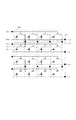
本実施例の固体撮像装置の上面図を図1(a)に示す。より具体的には、光電変換部が配された第1の半導体基板の上面図である。図1(a)のA−A´における断面図を図1(b)に示す。
100は画素領域である。画素を構成する要素が複数配された領域である。図では4×4の行列状に配されている。この構成に限らず更に多数の構成要素が配されていても良いし、ライン状に配されていても良い。
101は光電変換部である。入射光を電子とホールの電荷対に変換し、信号電荷として電子を収集する。例えばPN接合フォトダイオードを用いることができる。P型半導体領域がアノードとして機能し、アノードに基準電圧となる接地電位が供給される。
102は光電変換部の電荷をFDへ転送する転送トランジスタのゲート電極を構成するポリシリコンである。103はFDである。光電変換部101の電荷が転送トランジスタによって転送される。N型の半導体領域により構成される。
104a、bは転送トランジスタのゲートに駆動信号を供給する転送制御線である。
105は光電変換部に基準電圧を供給するための基準電圧供給線である。画素領域100内の複数の領域においてコンタクトプラグを介して光電変換部へ電位を供給する。コンタクトプラグが直接光電変換部を構成する半導体領域に接続されていても良いし、転送トランジスタのチャネル部を提供するP型半導体領域や、隣接画素間を分離するためのP型半導体領域を介して基準電圧を供給しても良い。転送トランジスタのチャネル部を提供するP型半導体領域はウエルと呼ぶこともでき、ウエル基準電圧を供給する場合には、基準電圧供給線はウエル電位供給線を兼ねることもできる。
106はFDとコンタクトプラグを介して電気的に接続される第1の電気的接続部である。FDと第2の半導体基板に配されたリセットトランジスタのソースもしくはドレイン及び増幅トランジスタのゲートの少なくとも一方と電気的に接続するためのである。本実施例においてはリセットトランジスタ及び増幅トランジスタの両者が第2の半導体基板に配される場合を説明するが、少なくとも一方が第2の半導体基板に配されていれば良い。両者が第2の半導体基板に配される場合には、FDとリセットトランジスタ及び増幅トランジスタの両者とが電気的に接続される。
109は第2の電気的接続部である。第2の電気的接続部109は基準電圧供給線105と第2の半導体基板に配された電源配線とを電気的に接続するものである。
107、108は第3の電気的接続部である。転送制御線104a、bと第2の半導体基板に配された転送走査回路とを電気的に接続するものである。
110はN型の半導体領域である。光電変換部を構成しており、信号電荷である電子を収集する。本実施例においては図面下方、つまり、トランジスタ及び配線が配される面とは反対側の主面から光が入射する裏面照射の構成となっている。
111はP型の半導体領域である。N型の半導体領域110とPN接合を構成する。光電変換部の共通アノードとして機能する。
112はP型の半導体領域である。転送トランジスタのチャネルを提供するための領域である。
113は高濃度のP型半導体領域である。高濃度P型半導体領域113は、コンタクトプラグ114を介して基準電圧供給線105と電気的に接続される。P型半導体領域111、112に基準電圧を与えるための領域である。
115はFDと第1の電気的接続部106とを電気的に接続するためのコンタクトプラグである。
Example 1
A top view of the solid-state imaging device of the present embodiment is shown in FIG. More specifically, it is a top view of a first semiconductor substrate on which a photoelectric conversion unit is arranged. FIG. 1B shows a cross-sectional view taken along line AA ′ of FIG.
104a and 104b are transfer control lines for supplying drive signals to the gates of the transfer transistors.
Reference numeral 111 denotes a P-type semiconductor region. A PN junction is formed with the N-
本実施例において第2の電気的接続部109は画素領域100の外部に配される。ここで第2の電気的接続部109の配置位置に関して説明する。
In the present embodiment, the second
比較例として第3の電気的接続部を画素領域100内に設けられた複数のコンタクトプラグ114に対応させて設けることもできる。この場合には、画素領域100内に複数設けられた第2の電気的接続部と、第2の電気的接続部に隣接する配線(基準電圧供給配線105を除く)とは一定以上の距離離す必要がある。この理由は、距離が短いと第1及び第2の半導体基板間を電気的に接続する工程において、第2の電気的接続部とこれに隣接する配線とのショートが発生しやすくなり点欠陥や線欠陥となるためである。
As a comparative example, the third electrical connection portion can be provided corresponding to the plurality of contact plugs 114 provided in the
したがって、例えば、転送制御線104bを図面上部に移動させて距離を確保する必要がある。しかしそうすると第1の電気的接続部106と転送制御線104bとの距離が近づく。第1の電気的接続部106と転送制御線104bとの距離を一定以上近づけるとFD容量値が上昇するため好ましくない。FDは転送された電荷をFDと周囲のP型半導体領域とにより構成するPN接合容量、及び寄生容量(これらを含めてFD容量とする)とにより電圧に変換する機能を有する。ここでFD容量値は画素の感度に直接結びつく。つまり、FD容量値が大きければ単位電荷量あたりの電位変化量は小さく、FD容量値が小さければ単位電荷量あたりの電位変化量は大きくなる。よって、FD容量値が小さい方が画素の感度を向上させることが可能となる。ここで、第1の電気的接続部106はFD103と電気的に接続されるため電気的には同一ノードとなる。このため第1の電気的接続部106と、第1の電気的接続部106に隣接する配線とにより生じる寄生容量はFD容量となる。つまり転送制御線104bが第1の電気的接続部106に近づくということはFD容量値が増えることにつながり感度を下げてしまうことにつながるのである。
Therefore, for example, it is necessary to secure the distance by moving the
これは本発明者らが新たに見出した、第1の半導体基板に配されたFDと、第2の半導体基板とを電気的に接続する際に新たに見出した課題である。FDは必ず画素毎もしくは複数の画素毎に電気的に接続されるため、第1の電気的接続部は画素領域内に設ける必要がある。そして第1の電気的接続部は確実な電気的接続を行うために一定以上の面積を確保する必要がある。第1の電気的接続部の面積を確保しつつ、画素領域内に電気的接続部を新たに増やすと、FD容量値の増加は避けられない。 This is a problem newly found by the present inventors when electrically connecting the FD disposed on the first semiconductor substrate and the second semiconductor substrate. Since the FD is always electrically connected to each pixel or a plurality of pixels, the first electrical connection portion needs to be provided in the pixel region. The first electrical connection portion needs to secure a certain area or more in order to perform reliable electrical connection. If the number of electrical connection portions is newly increased in the pixel region while securing the area of the first electrical connection portion, an increase in the FD capacitance value is inevitable.
これに対して本実施例のように、第2の電気的接続部109を画素領域外に配置することで、第1の電気的接続部の面積を一定以上確保しつつ、隣接する配線との距離を確保することができる。したがって、FD容量値の増加を抑制することが可能となり、感度を下げることなく光電変換部に基準電圧を供給することが可能となる。
On the other hand, as in this embodiment, the second
図2は第1の半導体基板に配される画素を構成する要素の電気的接続関係を示す等価回路図である。図1と同様の機能を有する部分には同一の符号を付し詳細な説明は省略する。
201は光電変換部、202は転送トランジスタ、203は第3の電気的接続部、204は第1の電気的接続部、205は第2の電気的接続部をそれぞれ示す。ここでは光電変換部としてフォトダイオードを用いている。フォトダイオードのカソードが転送トランジスタのソースと接続され、転送トランジスタのドレインがFDとなっている。フォトダイオードのカソードと転送トランジスタは同一半導体領域を用いて同一ノードとなっていればよい。点線で囲った部分が1画素を示している。
FIG. 2 is an equivalent circuit diagram showing an electrical connection relationship of elements constituting the pixel disposed on the first semiconductor substrate. Parts having the same functions as those in FIG. 1 are denoted by the same reference numerals, and detailed description thereof is omitted.
201 denotes a photoelectric conversion unit, 202 denotes a transfer transistor, 203 denotes a third electrical connection unit, 204 denotes a first electrical connection unit, and 205 denotes a second electrical connection unit. Here, a photodiode is used as the photoelectric conversion unit. The cathode of the photodiode is connected to the source of the transfer transistor, and the drain of the transfer transistor is FD. The cathode of the photodiode and the transfer transistor need only be the same node using the same semiconductor region. A portion surrounded by a dotted line indicates one pixel.
図3(a)に第2の半導体基板の上面図を示す。図3(b)に図3(a)のB−B´における断面図を示す。
301はリセットトランジスタ、302は増幅トランジスタである。点線内の斜め線でハッチングされた部分が各トランジスタのゲート電極を構成するポリシリコンである。ゲート電極を挟んで両側にソース、ドレイン領域が配されている。リセットトランジスタ301に比べて増幅トランジスタ302のゲート面積が大きい。このような構成とすることにより増幅トランジスタで発生する1/fノイズを抑制することが可能となる。ここでのゲート面積とはトランジスタのチャネル部を覆うポリシリコンの面積が1/fノイズに寄与するためチャネル部上の面積である。
303は第4の電気的接続部である。第1の半導体基板に配された第1の電気的接続部とマイクロバンプ等を介して電気的に接続される。更に、増幅トランジスタのゲート及びリセットトランジスタのソースと電気的に接続されている。
304はリセットトランジスタのドレインに電圧を供給するためのリセットドレイン供給配線である。305はリセットトランジスタのゲートに駆動信号を供給するためのリセットゲート制御線である。306はリセットトランジスタのソースと増幅トランジスタのゲートとを電気的に接続するためのローカル配線である。307は増幅トランジスタのドレインに電圧を供給するための電圧供給線である。
308は第5の電気的接続部である。第1の半導体基板の画素領域外に複数配された第2の電気的接続部とマイクロバンプ等を介して電気的に接続される。第5の電気的接続部も第2の電気的接続部と同様に画素領域外に複数設けられる。複数の第5の電気的接続部308には不図示の電源配線から基準電圧、例えば接地電位が供給されている。更に電源配線には第2の半導体基板外部から基準電圧が供給されている。
309は複数の第5の電気的接続部を接続する配線である。
310は第6の電気的接続部である。第1の半導体基板に配された第3の電気的接続部とマイクロバンプ等を介して電気的に接続される。
311は増幅トランジスタのゲートを構成するポリシリコンである。312は素子分離領域である。ポリシリコン311は増幅トランジスタのチャネル及び素子分離領域312の一部上部を覆って配されている。
FIG. 3A shows a top view of the second semiconductor substrate. FIG. 3B is a cross-sectional view taken along the line BB ′ of FIG.
Reference numeral 308 denotes a fifth electrical connection portion. A plurality of second electrical connection portions arranged outside the pixel region of the first semiconductor substrate are electrically connected through micro bumps or the like. Similar to the second electrical connection portion, a plurality of fifth electrical connection portions are also provided outside the pixel region. A reference voltage such as a ground potential is supplied to the plurality of fifth electrical connection portions 308 from a power supply wiring (not shown). Further, a reference voltage is supplied to the power supply wiring from the outside of the second semiconductor substrate.
Reference numeral 310 denotes a sixth electrical connection portion. It is electrically connected to a third electrical connection portion disposed on the first semiconductor substrate via a micro bump or the like.
図4は第2の半導体基板に配された画素の構成要素の電気的接続を示す等価回路図である。401はリセットトランジスタ、402は増幅トランジスタ、403は第4の電気的接続部、404は第5の電気的接続部、405は第6の電気的接続部を示している。リセットトランジスタのソースと増幅トランジスタのゲートとが電気的に接続されている。406は複数の画素からの信号が出力される共通出力線である。点線で囲った部分が1画素を示している。
FIG. 4 is an equivalent circuit diagram showing the electrical connection of the components of the pixel arranged on the second semiconductor substrate. 401 indicates a reset transistor, 402 indicates an amplification transistor, 403 indicates a fourth electrical connection, 404 indicates a fifth electrical connection, and 405 indicates a sixth electrical connection. The source of the reset transistor and the gate of the amplification transistor are electrically connected. A
図5(a)、(b)に各半導体基板の上面全体図を示す。
501a、bはそれぞれ第1、第2の半導体基板を示している。502a、502bは各半導体基板における画素領域を示している。各画素領域には画素を構成する構成要素が配されている。
503aは複数の第2の電気的接続部が配される領域である。503bは複数の第5の電気的接続部が配される領域である。504aは複数の第3の電気的接続部が配される領域である。504bは複数の第6の電気的接続部が配される領域である。503a、503bは一方が他方に対して垂直投影した時に一部、一方が他方の領域全て重なる位置に配されている。504a、504bは一方が他方に対して垂直投影した時に一部が重なる位置に配されている。
505は信号処理部である。一例として複数の画素からの信号を並列に処理可能な回路である。具体的には画素列毎に設けられた増幅器、CDS回路、AD変換器などである。複数のトランジスタを含んで構成され、これらのトランジスタは通常のスイッチもしくは演算増幅器の一部として機能している。
506は水平出力線である。水平出力線506は信号処理部505により並列に処理された後、直列信号に変換された信号を外部に読み出す。
507は水平走査部である。信号処理部505で処理された後の信号を直列信号に変換すべく順次パルスを供給する。上述の走査部と同様に信号処理部207で並列処理された信号を順次選択する機能を有していればよい。
508は水平出力線506から出力された信号を増幅して外部に出力する増幅部である。増幅部508は必要に応じて設けられる。
509は垂直走査部である。シフトレジスタ、デコーダを用いて形成することができる。転送制御線104a、リセット制御線305に対して順次駆動パルスを供給する。
5A and 5B are overall top views of each semiconductor substrate.
Reference numeral 506 denotes a horizontal output line. The horizontal output line 506 is processed in parallel by the
本実施例は第1の半導体基板に光電変換部へ基準電圧を供給する基準電圧供給線と、第2の半導体基板に電源配線とを電気的に接続する第2の電気的接続領域を第1の半導体基板の画素領域外に配した。このような配置とすることによりFD容量を上昇させることなく、光電変換部へ基準電圧を供給することが可能となる。 In this embodiment, a reference voltage supply line for supplying a reference voltage to the photoelectric conversion unit to the first semiconductor substrate and a second electrical connection region for electrically connecting the power supply wiring to the second semiconductor substrate are provided in the first. It was arranged outside the pixel region of the semiconductor substrate. With such an arrangement, it is possible to supply a reference voltage to the photoelectric conversion unit without increasing the FD capacity.
(実施例2)
図6(a)、(b)に本実施例の各半導体基板の上面全体図を示す。実施例1との違いは第1の半導体基板の画素領域内に基準電圧供給線105と第2の半導体基板に配された電源配線とを電気的に接続するための第7の電気的接続部を設けた点にある。それ以外の構成は実施例1と同様の構成であり、同様の機能を有する部分には同様の符号を付し詳細な説明は省略する。
(Example 2)
FIGS. 6A and 6B are overall top views of the semiconductor substrates of this embodiment. The seventh embodiment is different from the first embodiment in that a seventh electrical connection portion for electrically connecting the reference
本実施例においては画素領域内に第7の電気的接続部を設けた。しかしながら実施例1で述べたように第7の電気的接続部を画素領域内に配することによってFD容量値が上昇してしまう恐れがある。したがって本実施例においては、FDを第2の半導体基板と電気的に接続する第1の電気的接続部に比べて周期的に間引いて配置する。具体的に本実施例においては中央部に1つのみ配置している。具体的な構成としてこれに限定されず、少なくともFDと第2の半導体基板を接続する電気的接続部に比べて少数で間引いて配置すればよい。 In the present embodiment, a seventh electrical connection portion is provided in the pixel region. However, as described in the first embodiment, there is a possibility that the FD capacitance value is increased by disposing the seventh electrical connection portion in the pixel region. Therefore, in this embodiment, the FD is periodically thinned and arranged as compared with the first electrical connection portion that is electrically connected to the second semiconductor substrate. Specifically, in the present embodiment, only one is arranged at the center. The specific configuration is not limited to this, and it may be arranged by thinning out with a small number compared to at least the electrical connection portion connecting the FD and the second semiconductor substrate.
以上本発明に関して具体的に実施例を示したが、本発明はこれに限るものではなく発明の主旨を越えない限り適宜変更可能である。 The embodiments of the present invention have been specifically described above. However, the present invention is not limited to these embodiments, and various modifications can be made without departing from the spirit of the invention.
たとえば、FDを垂直方向の2画素の共有としたが、共有する画素はこれに限ったものではなく、更に、1画素につき1FDを有していてもよい。 For example, although the FD is shared by two pixels in the vertical direction, the shared pixels are not limited to this, and may further have 1 FD per pixel.
また第2の半導体基板の画素領域内に、電源配線からの基準電圧を供給する複数のコンタクトプラグを設けることもできる。第2の半導体基板の画素領域内にはリセットトランジスタ、増幅トランジスタが配されている。これらトランジスタが配されるウエル電位は各トランジスタの動作特性を決める上で重要である。このウエル電位が画素領域内の場所によって電位の分布が生じると、画素領域ごとに異なるオフセットとして信号にシェーディングが生じる場合がある。 In addition, a plurality of contact plugs for supplying a reference voltage from the power supply wiring can be provided in the pixel region of the second semiconductor substrate. A reset transistor and an amplifying transistor are arranged in the pixel region of the second semiconductor substrate. The well potential at which these transistors are arranged is important in determining the operating characteristics of each transistor. When the potential distribution of the well potential varies depending on the location in the pixel region, shading may occur in the signal as an offset different for each pixel region.
これに対して第2の半導体基板の画素領域内のウエルに複数のコンタクトプラグを介して基準電圧を供給することにより上記シェーディングを抑制することが可能となる。またコンタクトプラグは増幅トランジスタごとに設けても良いし、複数の増幅トランジスタごとに設けてもよい。増幅トランジスタのゲート面積を大きくして1/fノイズを抑制しつつ画素ピッチを微細化する場合には、全ての増幅トランジスタ毎ではなく複数の増幅トランジスタごとに間引いては位置するのがよい。 On the other hand, the shading can be suppressed by supplying a reference voltage to the well in the pixel region of the second semiconductor substrate via a plurality of contact plugs. The contact plug may be provided for each amplification transistor, or may be provided for each of a plurality of amplification transistors. In the case of reducing the pixel pitch while suppressing the 1 / f noise by increasing the gate area of the amplification transistor, it is preferable to thin out not every amplification transistor but every plurality of amplification transistors.
101 光電変換部
103 フローティングディフュージョン
106 第1の電気的接続部
109 第2の電気的接続部
301 リセットトランジスタ
302 増幅トランジスタ
DESCRIPTION OF
Claims (7)
各々が、前記複数のフローティングディフュージョンの各々にリセット電位を供給する、複数のリセットトランジスタと、
各々が、前記複数のフローティングディフュージョンの各々の電位変化に基づく信号を増幅して出力する、複数の増幅トランジスタと、
前記光電変換部に基準電圧を供給するための基準電圧供給線と、を有し、
前記画素領域及び前記基準電圧供給線が第1の半導体基板に配され、前記複数のリセットトランジスタもしくは前記複数の増幅トランジスタの少なくとも一方が第2の半導体基板に配された固体撮像装置であって、
前記基準電圧供給線に電圧を供給するための電源線が前記第2の半導体基板に配されており、
前記フローティングディフュージョンと、前記第2の半導体基板に配された前記リセットトランジスタ及び前記増幅トランジスタとを電気的に接続するための複数の第1の電気的接続部と、
前記基準電圧供給線と前記電源線とを電気的に接続するための複数の第2の電気的接続部と、を有し、
前記複数の第1の電気的接続部は前記画素領域内に配され、
前記複数の第2の電気的接続部は前記画素領域外に配されており、
前記第2の半導体基板の画素領域内に、前記第2の半導体基板の画素領域内のウエルに、前記電源線からの基準電圧を供給するための複数のコンタクトプラグが配されていることを特徴とする固体撮像装置。 A pixel region in which a plurality of photoelectric conversion units, floating diffusions, and transfer transistors that transfer charges of the photoelectric conversion units to the floating diffusions are disposed ;
A plurality of reset transistors , each supplying a reset potential to each of the plurality of floating diffusions;
Each amplifies and outputs a signal based on each of the potential change of said plurality of floating diffusion, a plurality of amplifying transistors,
A reference voltage supply line for supplying a reference voltage to the photoelectric conversion unit,
A solid-state imaging device in which the pixel region and the reference voltage supply line are disposed on a first semiconductor substrate, and at least one of the plurality of reset transistors or the plurality of amplification transistors is disposed on a second semiconductor substrate;
A power line for supplying a voltage to the reference voltage supply line is disposed on the second semiconductor substrate;
A plurality of first electrical connection portions for electrically connecting the floating diffusion and the reset transistor and the amplification transistor disposed on the second semiconductor substrate;
A plurality of second electrical connection parts for electrically connecting the reference voltage supply line and the power supply line,
The plurality of first electrical connections are disposed in the pixel region,
Second electrical connection of said plurality Ri Contact arranged outside the pixel region,
In the pixel region of the second semiconductor substrate, a plurality of contact plugs for supplying a reference voltage from the power supply line are arranged in a well in the pixel region of the second semiconductor substrate. A solid-state imaging device.
前記第1の半導体基板に、前記走査回路と電気的接続を行なう複数の第3の電気的接続部が配され、該複数の第3の電気的接続部は、前記画素領域外に配されていることを特徴とする請求項1に記載の固体撮像装置。 A scanning circuit for supplying a driving signal to the gate of the transfer transistor in the second semiconductor substrate;
A plurality of third electrical connection portions that are electrically connected to the scanning circuit are disposed on the first semiconductor substrate, and the plurality of third electrical connection portions are disposed outside the pixel region. The solid-state imaging device according to claim 1, wherein:
複数の前記増幅トランジスタごとに設けられていることを特徴とする請求項1〜4のいずれか1項に記載の固体撮像装置。 The plurality of contact plugs are:
The solid-state imaging device according to claim 1, wherein the solid-state imaging device is provided for each of the plurality of amplification transistors.
Priority Applications (4)
| Application Number | Priority Date | Filing Date | Title |
|---|---|---|---|
| JP2009288459A JP5558801B2 (en) | 2009-12-18 | 2009-12-18 | Solid-state imaging device |
| US13/515,445 US9177979B2 (en) | 2009-12-18 | 2010-12-13 | Solid-state image pickup device having reference voltage supply line on a first substrate and power supply lines to supply voltages to the reference voltage supply line on a second substrate |
| PCT/JP2010/007227 WO2011074235A1 (en) | 2009-12-18 | 2010-12-13 | Solid-state image pickup device |
| CN201080056461.0A CN102656693B (en) | 2009-12-18 | 2010-12-13 | Solid-state image pickup device |
Applications Claiming Priority (1)
| Application Number | Priority Date | Filing Date | Title |
|---|---|---|---|
| JP2009288459A JP5558801B2 (en) | 2009-12-18 | 2009-12-18 | Solid-state imaging device |
Publications (2)
| Publication Number | Publication Date |
|---|---|
| JP2011129784A JP2011129784A (en) | 2011-06-30 |
| JP5558801B2 true JP5558801B2 (en) | 2014-07-23 |
Family
ID=43719486
Family Applications (1)
| Application Number | Title | Priority Date | Filing Date |
|---|---|---|---|
| JP2009288459A Expired - Fee Related JP5558801B2 (en) | 2009-12-18 | 2009-12-18 | Solid-state imaging device |
Country Status (4)
| Country | Link |
|---|---|
| US (1) | US9177979B2 (en) |
| JP (1) | JP5558801B2 (en) |
| CN (1) | CN102656693B (en) |
| WO (1) | WO2011074235A1 (en) |
Families Citing this family (12)
| Publication number | Priority date | Publication date | Assignee | Title |
|---|---|---|---|---|
| JP6056126B2 (en) | 2011-10-21 | 2017-01-11 | ソニー株式会社 | Solid-state imaging device and camera system |
| JP6018376B2 (en) * | 2011-12-05 | 2016-11-02 | キヤノン株式会社 | Solid-state imaging device and camera |
| JP5961424B2 (en) | 2012-03-30 | 2016-08-02 | シスメックス株式会社 | Sample analyzer, sample analysis method, and sample analysis system |
| JP2014150231A (en) * | 2013-02-04 | 2014-08-21 | Toshiba Corp | Solid-state image pickup device manufacturing method therefor |
| JP6192391B2 (en) * | 2013-07-05 | 2017-09-06 | キヤノン株式会社 | Photoelectric conversion system |
| JP6257726B2 (en) * | 2016-09-30 | 2018-01-10 | キヤノン株式会社 | Solid-state imaging device and camera |
| JP6332420B2 (en) * | 2016-12-05 | 2018-05-30 | ソニー株式会社 | Semiconductor device, solid-state imaging device, and camera system |
| JP2017063493A (en) * | 2016-12-05 | 2017-03-30 | ソニー株式会社 | Semiconductor device, solid state image sensor and camera system |
| JP7171170B2 (en) * | 2017-06-29 | 2022-11-15 | キヤノン株式会社 | IMAGING DEVICE, IMAGING SYSTEM, MOVING OBJECT, METHOD FOR MANUFACTURING IMAGING DEVICE |
| JP6526159B2 (en) * | 2017-11-21 | 2019-06-05 | キヤノン株式会社 | Solid-state imaging device and camera |
| DE102018122798B4 (en) * | 2018-05-31 | 2021-02-11 | Taiwan Semiconductor Manufacturing Co. Ltd. | Solid state imaging device with improved dark current performance |
| US10797091B2 (en) | 2018-05-31 | 2020-10-06 | Taiwan Semiconductor Manufacturing Co., Ltd. | Semiconductor imaging device having improved dark current performance |
Family Cites Families (14)
| Publication number | Priority date | Publication date | Assignee | Title |
|---|---|---|---|---|
| JP3424360B2 (en) * | 1994-12-08 | 2003-07-07 | 株式会社日立製作所 | Solid-state imaging device |
| US5627082A (en) * | 1995-03-29 | 1997-05-06 | Texas Instruments Incorporated | High thermal resistance backfill material for hybrid UFPA's |
| JP3467013B2 (en) * | 1999-12-06 | 2003-11-17 | キヤノン株式会社 | Solid-state imaging device |
| JP4349232B2 (en) * | 2004-07-30 | 2009-10-21 | ソニー株式会社 | Semiconductor module and MOS solid-state imaging device |
| US7551059B2 (en) * | 2005-01-06 | 2009-06-23 | Goodrich Corporation | Hybrid infrared detector array and CMOS readout integrated circuit with improved dynamic range |
| WO2006073875A2 (en) * | 2005-01-06 | 2006-07-13 | Recon/Optical, Inc. | Cmos active pixel sensor with improved dynamic range and method of operation, method for identifying moving objects and hybrid array with ir detector |
| KR100782463B1 (en) * | 2005-04-13 | 2007-12-05 | (주)실리콘화일 | Separation type unit pixel of image sensor having 3 dimension structure and manufacture method thereof |
| US8049256B2 (en) * | 2006-10-05 | 2011-11-01 | Omnivision Technologies, Inc. | Active pixel sensor having a sensor wafer connected to a support circuit wafer |
| JP2008235478A (en) * | 2007-03-19 | 2008-10-02 | Nikon Corp | Imaging device |
| JP5223343B2 (en) | 2008-01-10 | 2013-06-26 | 株式会社ニコン | Solid-state image sensor |
| JP5269425B2 (en) * | 2008-01-29 | 2013-08-21 | 株式会社東芝 | Solid-state imaging device and solid-state imaging device |
| JP4630907B2 (en) * | 2008-03-03 | 2011-02-09 | シャープ株式会社 | Solid-state imaging device and electronic information device |
| US20090256156A1 (en) * | 2008-04-09 | 2009-10-15 | E-Phocus, Inc | Hybrid imaging sensor with approximately equal potential photodiodes |
| JP5078753B2 (en) | 2008-05-28 | 2012-11-21 | 株式会社フジシールインターナショナル | Virgin seal |
-
2009
- 2009-12-18 JP JP2009288459A patent/JP5558801B2/en not_active Expired - Fee Related
-
2010
- 2010-12-13 WO PCT/JP2010/007227 patent/WO2011074235A1/en active Application Filing
- 2010-12-13 CN CN201080056461.0A patent/CN102656693B/en not_active Expired - Fee Related
- 2010-12-13 US US13/515,445 patent/US9177979B2/en not_active Expired - Fee Related
Also Published As
| Publication number | Publication date |
|---|---|
| US20120248293A1 (en) | 2012-10-04 |
| US9177979B2 (en) | 2015-11-03 |
| JP2011129784A (en) | 2011-06-30 |
| WO2011074235A1 (en) | 2011-06-23 |
| CN102656693A (en) | 2012-09-05 |
| CN102656693B (en) | 2015-04-01 |
Similar Documents
| Publication | Publication Date | Title |
|---|---|---|
| JP5558801B2 (en) | Solid-state imaging device | |
| US11322535B2 (en) | Solid-state imaging device and camera | |
| JP4752447B2 (en) | Solid-state imaging device and camera | |
| JP5328224B2 (en) | Solid-state imaging device | |
| US7863661B2 (en) | Solid-state imaging device and camera having the same | |
| KR100820520B1 (en) | Solid state imaging apparatus | |
| KR20100002184A (en) | Solid-state imaging device and electronic apparatus | |
| JP6025750B2 (en) | Imaging device | |
| JP2015130533A (en) | Solid state imaging device and camera | |
| JP2011199185A (en) | Solid-state imaging device | |
| JP5581698B2 (en) | Solid-state image sensor | |
| JP5531081B2 (en) | Solid-state imaging device and camera | |
| JP2008071822A (en) | Mos solid-state image sensing device | |
| JP2020017753A (en) | Pixel unit and imaging element | |
| JP5725232B2 (en) | Solid-state imaging device and camera | |
| JP2017163607A (en) | Solid-state imaging device and electronic equipment | |
| JP2015012240A (en) | Imaging element and electronic apparatus | |
| JP2019195183A (en) | Solid-state image pickup device and electronic apparatus | |
| JP2013211295A (en) | Solid state image pickup device and method of manufacturing the same, and electronic equipment |
Legal Events
| Date | Code | Title | Description |
|---|---|---|---|
| A621 | Written request for application examination |
Free format text: JAPANESE INTERMEDIATE CODE: A621 Effective date: 20121218 |
|
| A131 | Notification of reasons for refusal |
Free format text: JAPANESE INTERMEDIATE CODE: A131 Effective date: 20140212 |
|
| A521 | Request for written amendment filed |
Free format text: JAPANESE INTERMEDIATE CODE: A523 Effective date: 20140414 |
|
| TRDD | Decision of grant or rejection written | ||
| A01 | Written decision to grant a patent or to grant a registration (utility model) |
Free format text: JAPANESE INTERMEDIATE CODE: A01 Effective date: 20140507 |
|
| A61 | First payment of annual fees (during grant procedure) |
Free format text: JAPANESE INTERMEDIATE CODE: A61 Effective date: 20140605 |
|
| R151 | Written notification of patent or utility model registration |
Ref document number: 5558801 Country of ref document: JP Free format text: JAPANESE INTERMEDIATE CODE: R151 |
|
| LAPS | Cancellation because of no payment of annual fees |