JP5546685B2 - Charger - Google Patents
Charger Download PDFInfo
- Publication number
- JP5546685B2 JP5546685B2 JP2013519241A JP2013519241A JP5546685B2 JP 5546685 B2 JP5546685 B2 JP 5546685B2 JP 2013519241 A JP2013519241 A JP 2013519241A JP 2013519241 A JP2013519241 A JP 2013519241A JP 5546685 B2 JP5546685 B2 JP 5546685B2
- Authority
- JP
- Japan
- Prior art keywords
- voltage
- control unit
- circuit block
- output
- transformer
- Prior art date
- Legal status (The legal status is an assumption and is not a legal conclusion. Google has not performed a legal analysis and makes no representation as to the accuracy of the status listed.)
- Active
Links
Images


Classifications
-
- B—PERFORMING OPERATIONS; TRANSPORTING
- B60—VEHICLES IN GENERAL
- B60L—PROPULSION OF ELECTRICALLY-PROPELLED VEHICLES; SUPPLYING ELECTRIC POWER FOR AUXILIARY EQUIPMENT OF ELECTRICALLY-PROPELLED VEHICLES; ELECTRODYNAMIC BRAKE SYSTEMS FOR VEHICLES IN GENERAL; MAGNETIC SUSPENSION OR LEVITATION FOR VEHICLES; MONITORING OPERATING VARIABLES OF ELECTRICALLY-PROPELLED VEHICLES; ELECTRIC SAFETY DEVICES FOR ELECTRICALLY-PROPELLED VEHICLES
- B60L53/00—Methods of charging batteries, specially adapted for electric vehicles; Charging stations or on-board charging equipment therefor; Exchange of energy storage elements in electric vehicles
- B60L53/20—Methods of charging batteries, specially adapted for electric vehicles; Charging stations or on-board charging equipment therefor; Exchange of energy storage elements in electric vehicles characterised by converters located in the vehicle
- B60L53/22—Constructional details or arrangements of charging converters specially adapted for charging electric vehicles
-
- H—ELECTRICITY
- H02—GENERATION; CONVERSION OR DISTRIBUTION OF ELECTRIC POWER
- H02J—CIRCUIT ARRANGEMENTS OR SYSTEMS FOR SUPPLYING OR DISTRIBUTING ELECTRIC POWER; SYSTEMS FOR STORING ELECTRIC ENERGY
- H02J7/00—Circuit arrangements for charging or depolarising batteries or for supplying loads from batteries
- H02J7/02—Circuit arrangements for charging or depolarising batteries or for supplying loads from batteries for charging batteries from ac mains by converters
-
- H—ELECTRICITY
- H02—GENERATION; CONVERSION OR DISTRIBUTION OF ELECTRIC POWER
- H02J—CIRCUIT ARRANGEMENTS OR SYSTEMS FOR SUPPLYING OR DISTRIBUTING ELECTRIC POWER; SYSTEMS FOR STORING ELECTRIC ENERGY
- H02J2207/00—Indexing scheme relating to details of circuit arrangements for charging or depolarising batteries or for supplying loads from batteries
- H02J2207/20—Charging or discharging characterised by the power electronics converter
-
- H—ELECTRICITY
- H02—GENERATION; CONVERSION OR DISTRIBUTION OF ELECTRIC POWER
- H02J—CIRCUIT ARRANGEMENTS OR SYSTEMS FOR SUPPLYING OR DISTRIBUTING ELECTRIC POWER; SYSTEMS FOR STORING ELECTRIC ENERGY
- H02J2310/00—The network for supplying or distributing electric power characterised by its spatial reach or by the load
- H02J2310/40—The network being an on-board power network, i.e. within a vehicle
- H02J2310/48—The network being an on-board power network, i.e. within a vehicle for electric vehicles [EV] or hybrid vehicles [HEV]
-
- H—ELECTRICITY
- H02—GENERATION; CONVERSION OR DISTRIBUTION OF ELECTRIC POWER
- H02M—APPARATUS FOR CONVERSION BETWEEN AC AND AC, BETWEEN AC AND DC, OR BETWEEN DC AND DC, AND FOR USE WITH MAINS OR SIMILAR POWER SUPPLY SYSTEMS; CONVERSION OF DC OR AC INPUT POWER INTO SURGE OUTPUT POWER; CONTROL OR REGULATION THEREOF
- H02M1/00—Details of apparatus for conversion
- H02M1/0067—Converter structures employing plural converter units, other than for parallel operation of the units on a single load
- H02M1/0077—Plural converter units whose outputs are connected in series
-
- H—ELECTRICITY
- H02—GENERATION; CONVERSION OR DISTRIBUTION OF ELECTRIC POWER
- H02M—APPARATUS FOR CONVERSION BETWEEN AC AND AC, BETWEEN AC AND DC, OR BETWEEN DC AND DC, AND FOR USE WITH MAINS OR SIMILAR POWER SUPPLY SYSTEMS; CONVERSION OF DC OR AC INPUT POWER INTO SURGE OUTPUT POWER; CONTROL OR REGULATION THEREOF
- H02M1/00—Details of apparatus for conversion
- H02M1/0083—Converters characterised by their input or output configuration
- H02M1/0085—Partially controlled bridges
-
- Y—GENERAL TAGGING OF NEW TECHNOLOGICAL DEVELOPMENTS; GENERAL TAGGING OF CROSS-SECTIONAL TECHNOLOGIES SPANNING OVER SEVERAL SECTIONS OF THE IPC; TECHNICAL SUBJECTS COVERED BY FORMER USPC CROSS-REFERENCE ART COLLECTIONS [XRACs] AND DIGESTS
- Y02—TECHNOLOGIES OR APPLICATIONS FOR MITIGATION OR ADAPTATION AGAINST CLIMATE CHANGE
- Y02T—CLIMATE CHANGE MITIGATION TECHNOLOGIES RELATED TO TRANSPORTATION
- Y02T10/00—Road transport of goods or passengers
- Y02T10/60—Other road transportation technologies with climate change mitigation effect
- Y02T10/70—Energy storage systems for electromobility, e.g. batteries
-
- Y—GENERAL TAGGING OF NEW TECHNOLOGICAL DEVELOPMENTS; GENERAL TAGGING OF CROSS-SECTIONAL TECHNOLOGIES SPANNING OVER SEVERAL SECTIONS OF THE IPC; TECHNICAL SUBJECTS COVERED BY FORMER USPC CROSS-REFERENCE ART COLLECTIONS [XRACs] AND DIGESTS
- Y02—TECHNOLOGIES OR APPLICATIONS FOR MITIGATION OR ADAPTATION AGAINST CLIMATE CHANGE
- Y02T—CLIMATE CHANGE MITIGATION TECHNOLOGIES RELATED TO TRANSPORTATION
- Y02T10/00—Road transport of goods or passengers
- Y02T10/60—Other road transportation technologies with climate change mitigation effect
- Y02T10/7072—Electromobility specific charging systems or methods for batteries, ultracapacitors, supercapacitors or double-layer capacitors
-
- Y—GENERAL TAGGING OF NEW TECHNOLOGICAL DEVELOPMENTS; GENERAL TAGGING OF CROSS-SECTIONAL TECHNOLOGIES SPANNING OVER SEVERAL SECTIONS OF THE IPC; TECHNICAL SUBJECTS COVERED BY FORMER USPC CROSS-REFERENCE ART COLLECTIONS [XRACs] AND DIGESTS
- Y02—TECHNOLOGIES OR APPLICATIONS FOR MITIGATION OR ADAPTATION AGAINST CLIMATE CHANGE
- Y02T—CLIMATE CHANGE MITIGATION TECHNOLOGIES RELATED TO TRANSPORTATION
- Y02T10/00—Road transport of goods or passengers
- Y02T10/80—Technologies aiming to reduce greenhouse gasses emissions common to all road transportation technologies
- Y02T10/92—Energy efficient charging or discharging systems for batteries, ultracapacitors, supercapacitors or double-layer capacitors specially adapted for vehicles
-
- Y—GENERAL TAGGING OF NEW TECHNOLOGICAL DEVELOPMENTS; GENERAL TAGGING OF CROSS-SECTIONAL TECHNOLOGIES SPANNING OVER SEVERAL SECTIONS OF THE IPC; TECHNICAL SUBJECTS COVERED BY FORMER USPC CROSS-REFERENCE ART COLLECTIONS [XRACs] AND DIGESTS
- Y02—TECHNOLOGIES OR APPLICATIONS FOR MITIGATION OR ADAPTATION AGAINST CLIMATE CHANGE
- Y02T—CLIMATE CHANGE MITIGATION TECHNOLOGIES RELATED TO TRANSPORTATION
- Y02T90/00—Enabling technologies or technologies with a potential or indirect contribution to GHG emissions mitigation
- Y02T90/10—Technologies relating to charging of electric vehicles
- Y02T90/14—Plug-in electric vehicles
Description
この発明は、電気自動車などの動力用バッテリを充電する充電装置に関する。 The present invention relates to a charging device for charging a power battery such as an electric vehicle.
地球温暖化ガスの排出量を削減する風潮の中で二酸化炭素排出量の少なさが受け入れられて電気自動車の需要が増加し普及が加速している。電気自動車に搭載される動力用(車載)バッテリは、充電装置を使用して外部の交流電源によって充電される。このような充電装置には、交流電源から効率よく電力を取り込むための力率改善用のコイル(リアクトル)や交流電源と動力用バッテリを絶縁する絶縁用のトランス、スイッチング素子、ダイオードが使用される。 With the trend of reducing global warming gas emissions, low carbon dioxide emissions have been accepted and the demand for electric vehicles has increased and the spread of these vehicles has accelerated. A power (on-vehicle) battery mounted on an electric vehicle is charged by an external AC power source using a charging device. In such a charging device, a power factor improving coil (reactor) for efficiently taking in electric power from an AC power source, an insulating transformer, a switching element, and a diode for insulating the AC power source from a power battery are used. .
例えば、特許文献1には、交流電源側にリアクトル(コイル)および当該リアクトルに電流を通電するスイッチと、出力側にトランスおよび当該トランスの1次巻線に電流を通電するスイッチとを備え、これらのスイッチを交互に動作させて力率を1に近づける電力変換器が記載されている。この電力変換器では、力率の改善と絶縁のためにリアクトルとトランスを使用している。なお、3相の交流を電源として使用し、それぞれの相間から3個の電力変換器に電力を入力し、3個の出力を並列に接続した構成についても開示されている。
For example,
特許文献2には、昇圧チョッパ回路による構成の力率改善回路(PFC;Power Factor Correction)と、絶縁型DC/DCコンバータ(第2電力変換回路)と、電源電圧が低下したときに出力電圧を補助する瞬低バックアップユニットを備えた電圧低下保護装置が開示されている。
また、特許文献3は、チョークコイル、スイッチングトランジスタおよびダイオードによるチョッパ回路を複数備え、これらチョッパ回路を並列に接続したコンバータ電源回路を開示する。このコンバータ電源回路は、並列に接続した複数のチョッパ回路のスイッチング素子を同じ周波数で駆動させながら、それぞれの駆動タイミングが重ならないように動作させている。
特許文献4は、フライバック型のトランスを使用して力率の改善を図った三相力率改善回路を開示する。この回路では、トランスの2次巻線側構成部材を並列に接続してフライバック電流を合成して平滑する。なお、特許文献4には、当該回路の駆動を制御する制御回路を、1次側と2次側を電気的に分離した絶縁型とした場合や、複数のインバータ回路のスイッチング素子にそれぞれ位相差をつけて動作させること、および単相交流電源に対応した構成についても記載されている。
さらに、特許文献5に記載の従来の充電器は、商用電源と回生電源を共用する充電器(商用回生共用充電器)であって、個々の電池にそれぞれのDC/DCコンバータで充電を行う構成の車両搭載の直列接続電池列に対して、駆動(回生)モータの回生電流を、上記DC/DCコンバータを介して充電に使用する。また、特許文献5には、商用電源からの充電において、上記DC/DCコンバータとは別に高力率AC/DCコンバータを設けた構成についても開示されている。
Furthermore, the conventional charger described in
従来、力率の改善や絶縁に関しては、個々の回路技術が熟成されてきている。
しかし、電気自動車用の充電装置では、車両が移動先で充電するときの現地の交流電源の環境および蓄電量によって変動するバッテリ電圧に対応する特性が必要である。例えば、条件の悪い電源電圧と出力電圧が組み合わされた場合は、スイッチング素子あるいは整流ダイオードに高い電圧が印加されるため、定格電圧の高いスイッチング素子あるいは整流ダイオードを使用する必要がある。なお、電気自動車用の充電装置は、大容量であり、使用する部品は必然的に電流定格も高い部品である。Conventionally, individual circuit technologies have been matured for power factor improvement and insulation.
However, a charging device for an electric vehicle requires characteristics corresponding to the battery voltage that varies depending on the environment of the local AC power supply and the amount of stored electricity when the vehicle is charged at the destination. For example, when a power supply voltage and an output voltage having poor conditions are combined, a high voltage is applied to the switching element or the rectifier diode, and therefore it is necessary to use a switching element or rectifier diode having a high rated voltage. In addition, the charging device for electric vehicles has a large capacity, and the parts to be used are inevitably parts having a high current rating.
さらに、充電装置に使用する各素子には高速の動作も必要となるため、上記定格電圧の高いスイッチング素子あるいは整流ダイオードの大型化、高コスト化を招きやすい。
例えば、特許文献1,2は、コイルとトランスを組み合わせた構成であり、特許文献4では、トランスを使用する構成であるため、電源電圧と出力電圧がともに高い場合には、スイッチング素子あるいは整流ダイオードに印加される電圧が高くなる可能性がある。
従って、どのような電源環境でも充電ができる電気自動車用の充電装置には、定格電圧が充分に高いスイッチング素子あるいは整流ダイオードを使用する必要がある。Furthermore, since each element used in the charging apparatus needs to operate at high speed, the switching element or the rectifier diode having a high rated voltage is likely to be increased in size and cost.
For example,
Therefore, it is necessary to use a switching element or a rectifier diode having a sufficiently high rated voltage for a charging device for an electric vehicle that can be charged in any power supply environment.
また、特許文献3では、コイルを使用した昇圧回路を構成しているので、交流電源と動力用(車載)バッテリとの絶縁ができない上に、高い電圧の交流電源から低い電圧のバッテリを充電することができず、電気自動車用の充電装置として好ましくない。
特許文献5に記載の充電器は、直列に接続された個々のバッテリを、それぞれの充電器で充電する構成である。この充電器は、独立した力率を改善するAC/DCコンバータを別にあつらえて使用しており、構成部材の数を低減する配慮がなされておらず、スイッチング素子あるいは整流ダイオードに印加される電圧を低減する工夫もない。また、個々のバッテリを充電するために接続される配線の数量が多く、その上に各配線は、大電流を通電するために充分な太さが必要になるため、機器内へ複数の配線を配策することが困難である。Further, in
The charger described in
この発明は、上記のような課題を解決するためになされたもので、簡素な構成で、安価かつ小型な充電装置を得ることを目的とする。 The present invention has been made to solve the above-described problems, and an object thereof is to obtain an inexpensive and small-sized charging device with a simple configuration.
この発明に係る充電装置は、交流電源で車両に搭載された動作用のバッテリを充電するものであって、交流電源を直流出力に整流する整流部と、力率改善用のコイルを兼用する1次巻線および交流電源と車両とを絶縁する2次巻線を有するトランス、トランスの1次巻線を流れる電流を断続するスイッチング素子、トランスの2次巻線から出力した電流を整流するダイオードおよびダイオードから出力した電流を蓄えて平滑する平滑コンデンサによって構成され、スイッチング素子のオンオフ動作により整流部の直流出力から所定の直流電力をそれぞれ出力する複数の回路ブロック部と、前記複数の回路ブロック部のそれぞれが有するスイッチング素子のオンオフ動作を制御する制御部とを備え、前記複数の回路ブロック部の1次側の構成をそれぞれ並列に接続し、前記複数の回路ブロック部の2次側の構成をそれぞれ直列に接続して構成され、前記複数の回路ブロック部のそれぞれが有する平滑コンデンサの電圧を入力する平滑コンデンサ電圧入力部を備え、前記制御部は、前記平滑コンデンサ電圧入力部により入力された前記各平滑コンデンサの電圧が同等となるように制御するもの、または、前記複数の回路ブロック部のそれぞれが有するスイッチング素子に印加される電圧を入力するスイッチング素子印加電圧入力部を備え、前記制御部は、前記スイッチング素子印加電圧入力部により入力された前記各スイッチング素子に印加される電圧が同等となるように制御するものである。 The present invention engaging Ru charging device is for charging the battery for operation mounted on the vehicle by an AC power source, also serves a rectifying unit for rectifying an AC power into a DC output, the coil for power factor improvement A transformer having a primary winding and a secondary winding that insulates the vehicle from an AC power source, a switching element for intermittently passing a current flowing through the primary winding of the transformer, and a current rectified from the secondary winding of the transformer A plurality of circuit block units each including a diode and a smoothing capacitor that stores and smooths the current output from the diode, and outputs predetermined DC power from a DC output of the rectifier unit by an on / off operation of the switching element; and the plurality of circuit blocks A control unit that controls the on / off operation of the switching element included in each of the units, and the configuration of the primary side of the plurality of circuit block units Connected to respectively parallel, the plurality of constructed by respectively connected in series to the secondary structure of the circuit block unit, a smoothing capacitor voltage input voltage of the smoothing capacitor, each of said plurality of circuit blocks section has An input unit, and the control unit controls the smoothing capacitor voltage input by the smoothing capacitor voltage input unit to be equal to each other, or the switching element included in each of the plurality of circuit block units A switching element application voltage input unit that inputs a voltage applied to the switching element, and the control unit controls the voltages applied to the switching elements input by the switching element application voltage input unit to be equal to each other. Is .
この発明によれば、簡素な構成で安価かつ小型な充電装置を提供することができるという効果がある。 According to the present invention, there is an effect that an inexpensive and small-sized charging device can be provided with a simple configuration.
以下、この発明をより詳細に説明するため、この発明を実施するための形態について、添付の図面に従って説明する。
実施の形態1.
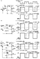
図1は、様々な構成の昇圧回路ブロックおよびその動作特性を示す図であり、スイッチング素子であるFET(電界効果トランジスタ)の動作信号、FETの印加電圧波形および整流ダイオードの印加電圧波形を示している。
図1(a)に示す回路ブロックは、コイルに流れる電流をFETによって断続するものであり、FETがオンしているときにコイルとコアに蓄えた磁気エネルギを、FETをオフにしたときに吐き出す昇圧電源の構成をしている。この回路では、交流の1サイクルの中で電源電圧が低下するタイミングにおいても電力を出力することができ、高い力率で出力電圧の昇圧が可能である。Hereinafter, in order to describe the present invention in more detail, modes for carrying out the present invention will be described with reference to the accompanying drawings.
FIG. 1 is a diagram showing booster circuit blocks of various configurations and their operating characteristics, showing operation signals of FETs (field effect transistors) that are switching elements, applied voltage waveforms of FETs, and applied voltage waveforms of rectifier diodes. Yes.
In the circuit block shown in FIG. 1A, the current flowing through the coil is interrupted by the FET, and when the FET is turned on, the magnetic energy stored in the coil and the core is discharged when the FET is turned off. It has a boost power supply configuration. In this circuit, electric power can be output even at the timing when the power supply voltage drops during one AC cycle, and the output voltage can be boosted with a high power factor.
また、この回路では、FETに印加される電圧は略出力電圧であり、整流ダイオードに印加される電圧も略出力電圧である。つまり、電源電圧を100V、出力電圧を200Vとした場合、図1(a)に示すように、FETおよび整流ダイオードにそれぞれ印加される電圧は概ね200Vとなる。
例えば、交流電源の最大電圧を250Vrms(整流部の出力電圧は350Vdc)、電気自動車用バッテリの最大電圧を400Vdcとした場合、FETと整流ダイオードとに印加される最高電圧は400Vであり、汎用的な400V対応のFETと整流ダイオードを使用することができる。
しかしながら、特許文献3に記載されるように、この回路構成では、交流電源とバッテリ(車載機器)の絶縁ができず、例えば250Vrmsの交流電源から電源電圧よりも低電圧の例えば80Vdcのバッテリを充電することができないため、電気自動車用バッテリの充電装置として使用できない。In this circuit, the voltage applied to the FET is substantially an output voltage, and the voltage applied to the rectifier diode is also an approximate output voltage. That is, when the power supply voltage is 100 V and the output voltage is 200 V, the voltage applied to the FET and the rectifier diode is approximately 200 V, as shown in FIG.
For example, when the maximum voltage of the AC power supply is 250 Vrms (the output voltage of the rectifier is 350 Vdc) and the maximum voltage of the battery for the electric vehicle is 400 Vdc, the maximum voltage applied to the FET and the rectifier diode is 400 V, A 400V compatible FET and rectifier diode can be used.
However, as described in
図1(b)に示す回路ブロックは、トランスの1次巻線に流れる電流をFETによって断続する。つまり、FETがオンしているとき、トランスの1次巻線とコアに蓄えた磁気エネルギを、FETをオフにしたときに、トランスの二次巻線に吐き出させるフライバック式電源を構成している。この回路構成では、交流の1サイクルの中で電源電圧が低下するタイミングにおいても電力を出力することができ、高い力率で、電圧を昇圧あるいは降圧することと、1次側と2次側の絶縁が同時に実現可能である。 In the circuit block shown in FIG. 1B, the current flowing through the primary winding of the transformer is interrupted by the FET. In other words, when the FET is on, a flyback power supply is constructed that discharges the magnetic energy stored in the transformer primary winding and core to the transformer secondary winding when the FET is turned off. Yes. In this circuit configuration, electric power can be output even at the timing when the power supply voltage decreases in one cycle of alternating current, and the voltage is increased or decreased at a high power factor, and the primary side and the secondary side are output. Insulation can be realized simultaneously.
この回路において、トランスの1次と2次の巻数比を1:nとした場合、FETに印加される電圧は、概ね((出力電圧/n)+電源電圧)であり、整流ダイオードに印加される電圧は、概ね(出力電圧+(n×電源電圧))である。つまり、電源電圧を100V、出力電圧を200V、n=1とした場合は、図1(b)に示すように、FETおよび整流ダイオードにそれぞれ印加される電圧は、概ね300Vとなる。 In this circuit, when the primary and secondary turns ratio of the transformer is 1: n, the voltage applied to the FET is approximately ((output voltage / n) + power supply voltage), and is applied to the rectifier diode. Is approximately (output voltage + (n × power supply voltage)). That is, when the power supply voltage is 100 V, the output voltage is 200 V, and n = 1, as shown in FIG. 1B, the voltages applied to the FET and the rectifier diode are approximately 300 V, respectively.
例えば、交流電源の最大電圧を250Vrms(整流部の出力電圧は350Vdc)、電気自動車用バッテリの最大電圧を400Vdc、nを1とした場合には、FETに印加される最高電圧は400V/1+350V=750Vとなり、整流ダイオードに印加される最高電圧は400V+350V/1=750Vとなる。
この場合、750V以上に対応するFETと整流ダイオードを使用せざるを得ないが、当該電圧に対応するFETやダイオード、特に動作速度が速く、大電流を通電することが可能なFETやダイオードは、汎用的なものが少なく、大型化する傾向があるため、製品化したときの装置のサイズやコストの観点から好適なものを選定することがし難い。For example, when the maximum voltage of the AC power supply is 250 Vrms (the output voltage of the rectifying unit is 350 Vdc), the maximum voltage of the battery for the electric vehicle is 400 Vdc, and n is 1, the maximum voltage applied to the FET is 400 V / 1 + 350 V = 750V, and the maximum voltage applied to the rectifier diode is 400V + 350V / 1 = 750V.
In this case, FETs and rectifier diodes corresponding to 750 V or more must be used, but FETs and diodes corresponding to the voltages, particularly FETs and diodes that have a high operating speed and can carry a large current, Since there are few general purpose things and there exists a tendency to enlarge, it is difficult to select a suitable thing from the viewpoint of the size and cost of the apparatus when commercialized.
図1(c)に示す回路は、力率改善用のコイルと絶縁用を兼ねたフライバック式トランスを用いた複数の回路ブロックを、トランスの1次側を並列に接続し、2次側を直列に接続して構成したものである。この構成では、図1(b)に示した回路と比べてそれぞれのトランス、FET、整流ダイオードの電力定格は1/2となる。従って、それぞれのトランス、FET、整流ダイオードには、定格電圧が低く、小型のものを使用することができる。 In the circuit shown in FIG. 1 (c), a plurality of circuit blocks using a flyback transformer that doubles as a power factor improving coil and an insulation are connected in parallel on the primary side of the transformer. It is configured by connecting in series. In this configuration, the power rating of each transformer, FET, and rectifier diode is ½ compared to the circuit shown in FIG. Therefore, each transformer, FET, and rectifier diode can have a low rated voltage and can be small.
この回路では、FETに印加される電圧が、概ね((出力電圧/2n)+電源電圧)であり、整流ダイオードに印加される電圧は、概ね(出力電圧/2+(n×電源電圧))である。つまり、電源電圧を100V、出力電圧を200V、n=1の場合、図1(c)に示すように、FETおよび整流ダイオードにそれぞれ印加される電圧は、概ね200Vとなる。 In this circuit, the voltage applied to the FET is approximately ((output voltage / 2n) + power supply voltage), and the voltage applied to the rectifier diode is approximately (output voltage / 2 + (n × power supply voltage)). is there. That is, when the power supply voltage is 100 V, the output voltage is 200 V, and n = 1, the voltage applied to the FET and the rectifier diode is approximately 200 V as shown in FIG.
例えば、交流電源の最大電圧を250Vrms(整流部の出力電圧は350Vdc)、電気自動車用バッテリの最大電圧を400Vdc、nを1とした場合には、FETに印加される最高電圧は、400V/2+350V=550Vとなり、整流ダイオードに印加される最高電圧は、400V/2+350V/1=550Vとなる。 For example, when the maximum voltage of the AC power supply is 250 Vrms (the output voltage of the rectifying unit is 350 Vdc), the maximum voltage of the battery for the electric vehicle is 400 Vdc, and n is 1, the maximum voltage applied to the FET is 400 V / 2 + 350 V = 550V, and the maximum voltage applied to the rectifier diode is 400V / 2 + 350V / 1 = 550V.
また、上記回路ブロックの数をN個とした場合には、図1(b)に示した回路と比べてそれぞれのトランス、FET、整流ダイオードの電力定格は1/Nとなる。従って、それぞれのトランス、FET、整流ダイオードには、さらに、定格電圧が低く、小型のものを使用することができる。 When the number of circuit blocks is N, the power rating of each transformer, FET, and rectifier diode is 1 / N compared to the circuit shown in FIG. Accordingly, each transformer, FET, and rectifier diode can be further small in rated voltage and small.
この回路では、各トランスの1次と2次の巻数比を1:nとした場合に、FETに印加される電圧は、概ね((出力電圧/(N×n))+電源電圧)であり、整流ダイオードに印加される電圧は、概ね(出力電圧/N+(n×電源電圧))である。
従って、交流電源の最大電圧を250Vrms(整流部の出力電圧は350Vdc)、電気自動車用バッテリの最大電圧を400Vdc、nを1、Nを8とした場合、FETに印加される最高電圧が400V/8+350V=400Vとなり、整流ダイオードに印加される最高電圧が400V/8+350V/1=400Vとなるので、FETおよび整流ダイオードに、図1(a)の構成と略同等の電圧定格のものが使用できる。In this circuit, when the primary and secondary turns ratio of each transformer is 1: n, the voltage applied to the FET is approximately ((output voltage / (N × n)) + power supply voltage). The voltage applied to the rectifier diode is approximately (output voltage / N + (n × power supply voltage)).
Therefore, when the maximum voltage of the AC power supply is 250 Vrms (the output voltage of the rectifying unit is 350 Vdc), the maximum voltage of the battery for the electric vehicle is 400 Vdc, n is 1, and N is 8, the maximum voltage applied to the FET is 400 V / Since 8 + 350V = 400V, and the maximum voltage applied to the rectifier diode is 400V / 8 + 350V / 1 = 400V, a FET and a rectifier diode having a voltage rating substantially equivalent to the configuration of FIG. 1A can be used.
このように、上記回路ブロックの数量を増やして、トランスの1次側を並列に接続し、2次側を直列に接続した回路とすれば、汎用性が高く、定格電圧の低いFETおよび整流ダイオードを使用することができ、製品化したときの装置のサイズやコストの観点から好適な選定が可能となる。 Thus, if the number of the circuit blocks is increased and the primary side of the transformer is connected in parallel and the secondary side is connected in series, the FET and the rectifier diode with high versatility and low rated voltage are provided. Can be used, and suitable selection is possible from the viewpoint of the size and cost of the apparatus when it is commercialized.
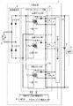
図2は、この発明の実施の形態1に係る充電装置の構成を示す図である。図2において、実施の形態1に係る充電装置1は、交流電源2から電気自動車用バッテリ3を充電する装置であって、電源整流部5、PFC(力率改善)・DC/DCコンバータ部6、平滑コンデンサ電圧入力部8および制御部9を備える。電気自動車用バッテリ3は、電気自動車の動力用モータなどの高電圧の負荷4と接続される。
FIG. 2 is a diagram showing a configuration of the charging apparatus according to
電源整流部5は、全波整流用に接続されたダイオード5−1,5−3、および、5−2,5−4を備えている。また、ダイオード5−1,5−2の各アノード端子は、低電位側出力となり、回路ブロック部7−1〜7−NのそれぞれのFETのソース端子と接続し、ダイオード5−3,5−4の各カソード端子は、高電位側出力となり、回路ブロック部7−1〜7−Nのそれぞれのトランスの1次巻線の一端(FETと接続しない方の端子)と接続している。さらに、交流電源2の一方の出力端子がダイオード5−1,5−3の接続点と接続し、交流電源2の他方の出力端子がダイオード5−2,5−4の接続点に接続している。
The power
PFC・DC/DCコンバータ部6は、100Vrms系または200Vrms系などの各種の交流電源2を電源として、80Vdc程度から400Vdc程度に変動する電気自動車用(動力用)の直流電圧を生成する構成部であり、複数(N個)の回路ブロック部7−1〜7−Nから構成される。
各回路ブロック部7−1〜7−Nは、トランス、FET(電界効果トランジスタ)、整流ダイオードおよび平滑コンデンサから構成されるDC/DCコンバータである。回路ブロック部7−1〜7−Nのトランスは、力率改善用のコイルを兼用する1次巻線および交流電源2と車両の電源とを絶縁する2次巻線を備えたフライバック式のトランスである。FETは、当該トランスの1次巻線への通電電流を断続するスイッチング素子である。整流ダイオードは、当該トランスの2次巻線からの出力電流を整流する。平滑コンデンサは、当該整流ダイオードの出力電流を蓄えて平滑する。
また、回路ブロック部7−1〜7−Nは、図1に示すようにそれぞれのトランスの1次側の構成部材(トランスの1次巻線の一方の端子(FETと接続しない方の端子)と当該FETのソース端子)が並列に接続され、2次側の構成部材(平滑コンデンサを介した2つの出力端子)が直列に接続される。The PFC / DC /
Each of the circuit block units 7-1 to 7-N is a DC / DC converter including a transformer, a FET (field effect transistor), a rectifier diode, and a smoothing capacitor. The transformers of the circuit block units 7-1 to 7-N are of a flyback type having a primary winding that also serves as a power factor improving coil and a secondary winding that insulates the
Further, as shown in FIG. 1, the circuit block units 7-1 to 7-N are composed of primary components of each transformer (one terminal of the transformer primary winding (terminal not connected to the FET)). And the source terminal of the FET) are connected in parallel, and the secondary side component (two output terminals via a smoothing capacitor) are connected in series.
平滑コンデンサ電圧入力部8は、回路ブロック部7−1〜7−Nのそれぞれの平滑コンデンサに印加される電圧を入力し、制御部9へ出力する。
制御部9は、回路ブロック部7−1〜7−Nの動作を制御する構成部であり、回路ブロック部7−1〜7−NのそれぞれのFETのゲート端子へ出力した回路ブロックFET駆動信号によって各FETのオンオフ動作を制御してトランスに磁気エネルギを蓄え、これを放出することで、トランスで発生した電流を整流ダイオードで整流し、平滑コンデンサで平滑して直流電圧を生成する。
また、実施の形態1では、制御部9は、平滑コンデンサ電圧入力部8を介して得られた各平滑コンデンサの電圧が均等になるように、各回路ブロック部7−1〜7−NのそれぞれのFETのオンオフ動作(周期およびDuty)を操作し、それぞれのFETに対して動作を間欠にする制御やPWM制御を行う。The smoothing capacitor voltage input unit 8 inputs a voltage applied to each smoothing capacitor of the circuit block units 7-1 to 7-N, and outputs the voltage to the
The
Further, in the first embodiment, the
図1(c)および図2に示すように、本発明では、力率改善用のコイルを兼用する絶縁用のトランス、FET、整流ダイオードおよび平滑コンデンサから構成される複数の回路ブロック部を用いて一式の充電装置を構成する。このように構成することで、各回路ブロック部7−1〜7−Nにおいて、FETおよび整流ダイオードに汎用的な定格電圧の低いものを使用しながら、力率改善用のコイルを使用することなく、簡素な構成で安価な充電装置を実現できる。なお、充電装置1は、電気自動車用(動力用)のバッテリ3を充電する出力端子は2端子であるため、特許文献5のように個々のバッテリに接続する複数の太い配線を配策する必要がなく、機構的な設計自由度の高い構成となる。
As shown in FIG. 1 (c) and FIG. 2, the present invention uses a plurality of circuit block units composed of an insulating transformer, FET, rectifier diode, and smoothing capacitor that also serve as a power factor improving coil. A set of charging devices is configured. By configuring in this way, in each of the circuit block units 7-1 to 7-N, a FET having a low general-purpose rated voltage is used for the FET and the rectifier diode, and without using a power factor improving coil. An inexpensive charging device can be realized with a simple configuration. In addition, since the
回路ブロック部7−1〜7−Nには、スイッチング速度の速いFETの他に、例えば、IGBT(Insulated Gate Bipolar Transistor)などの各種のトランジスタを使用し、整流ダイオードに、逆回復時間の短いファーストリカバリ型ダイオード(FRD)を使用してもよい。一般的にはスイッチング素子および整流ダイオードを使用する機器の回路電圧が500Vdcを超えると、これに対応する定格電圧のスイッチング素子および整流ダイオードが格段に少なくなり、素子選択の自由度が低下する。また、回路電圧が高くなると、各素子の耐電圧を確保するためにスイッチング速度および逆回復時間などの一部の電気的特性をトレードオフすることもあり、スイッチング素子あるいは整流ダイオードを選択する設計的な自由度も限られる。さらに、流通数量の少ない素子のコストは一般的に割高である。
同様に、平滑コンデンサは、電源の力率を改善しながらリプルの少ない直流電流をバッテリ3へ出力するフィルタ機能を有するため、従来の充電装置では、交流電源2の2倍の周波数のリプルを吸収すべく、高耐電圧で大容量のコンデンサ(例えば、電解コンデンサあるいはスーパーキャパシタ)を使用せざるを得なかった。このように、従来では、平滑コンデンサについても、素子選択の自由度が低く、コストも必然的に割高なものとなっていた。In the circuit block units 7-1 to 7-N, various transistors such as an IGBT (Insulated Gate Bipolar Transistor) are used in addition to an FET having a high switching speed, and the rectifier diode has a fast reverse recovery time. A recovery diode (FRD) may be used. Generally, when the circuit voltage of a device using a switching element and a rectifier diode exceeds 500 Vdc, the switching elements and rectifier diodes having a rated voltage corresponding to the circuit voltage are remarkably reduced, and the degree of freedom in element selection is reduced. In addition, when the circuit voltage increases, some electrical characteristics such as switching speed and reverse recovery time may be traded off to ensure the withstand voltage of each element. The degree of freedom is also limited. Furthermore, the cost of an element with a small distribution quantity is generally high.
Similarly, the smoothing capacitor has a filter function that outputs a DC current with less ripple to the
そこで、本発明では、図1(c)および図2に示すように、DC/DCコンバータとして機能する複数個の回路ブロック部7−1〜7−Nを用いて、それぞれのトランスの1次側の構成部材を並列に接続し、2次側の構成部材を直列に接続して一式の充電装置を構成する。このように構成することで、個々の回路ブロック部には、定格電圧の低い汎用的な素子を利用でき、自ずと高速動作が可能な素子を選択する自由度が向上する。例えば、DC/DCコンバータ構成のスイッチング周波数を高くすることができれば、小型のコイルやトランスを使用できる。 Therefore, in the present invention, as shown in FIG. 1C and FIG. 2, a plurality of circuit block units 7-1 to 7-N functioning as DC / DC converters are used, and the primary side of each transformer. These components are connected in parallel, and the secondary components are connected in series to form a set of charging devices. With this configuration, a general-purpose element having a low rated voltage can be used for each circuit block unit, and the degree of freedom for selecting an element that can naturally operate at high speed is improved. For example, if the switching frequency of the DC / DC converter configuration can be increased, a small coil or transformer can be used.
なお、本発明は、一式の充電装置を構成するトランス、FETおよび平滑コンデンサを複数に分割したものと等価になるが、それぞれのトランス、FETおよび平滑コンデンサを小型にすることができるため、各素子の配置の自由度も向上して、結果的に充電装置1全体を小型化することが可能である。
特に、各素子が小型になると、簡素な固定手段でそれぞれの素子を容易に固定することができ、大きな振動が加わる可能性がある車載用の充電装置に好適である。
さらに、汎用的な定格電圧の低いトランス、FETおよび平滑コンデンサは、低コストであるため、充電装置1を安価に構成できる。The present invention is equivalent to a transformer, FET, and smoothing capacitor that constitute a set of charging devices, but each transformer, FET, and smoothing capacitor can be reduced in size. As a result, the
In particular, when each element is reduced in size, each element can be easily fixed with a simple fixing means, which is suitable for an in-vehicle charging apparatus in which a large vibration may be applied.
Furthermore, since a general-purpose transformer, FET, and smoothing capacitor having a low rated voltage are low in cost, the charging
また、この実施の形態1では、制御部9が、平滑コンデンサ電圧入力部8を介して入力した回路ブロック部7−1〜7−Nのそれぞれの平滑コンデンサの電圧が略同等になるように、回路ブロック部7−1〜7−NのそれぞれのFETのオンオフ動作(周期およびDuty)を制御する。このように制御することで、回路ブロック部7−1〜7−Nの各平滑コンデンサに印加される電圧がばらばらになり、その一部の平滑コンデンサに印加される電圧が過大になって当該平滑コンデンサが劣化、さらには破壊することを防止できる。これにより、平滑コンデンサに負担を掛けない信頼性の高い充電装置を構成できる。
In the first embodiment, the
以上のように、この実施の形態1では、交流電源2で車両に搭載された動作用のバッテリを充電する充電装置1であって、交流電源2を直流出力に整流する電源整流部5と、力率改善用のコイルを兼用する1次巻線および交流電源2と車両とを絶縁する2次巻線を有するトランス、トランスの1次巻線を流れる電流を断続するスイッチング素子であるFET、トランスの2次巻線から出力した電流を整流する整流ダイオードおよび整流ダイオードから出力した電流を蓄えて平滑する平滑コンデンサによって構成され、FETのオンオフ動作により電源整流部5の直流出力から所定の直流電力をそれぞれ出力する複数の回路ブロック部7−1〜7−Nと、複数の回路ブロック部7−1〜7−Nのそれぞれが有するFETのオンオフ動作を制御する制御部とを備え、複数の回路ブロック部7−1〜7−Nの1次側の構成をそれぞれ並列に接続し、複数の回路ブロック部7−1〜7−Nの2次側の構成をそれぞれ直列に接続する。このように構成したので、簡素な構成で安価かつ小型の充電装置1を提供することができる。
As described above, in the first embodiment, the
また、この実施の形態1によれば、制御部9が、回路ブロック部7−1〜7−Nの各平滑コンデンサに印加される電圧が略同等になるようにFETのオンオフ動作(周期およびDuty)を制御する。特に、回路ブロック部7−1〜7−Nのそれぞれが有する平滑コンデンサの電圧を入力する平滑コンデンサ電圧入力部8を備え、制御部9が、平滑コンデンサ電圧入力部8により入力された各平滑コンデンサの電圧が略同等となるように制御する。このようにすることで、回路ブロック部7−1〜7−Nの各平滑コンデンサに印加される電圧がばらばらになり、その一部の平滑コンデンサが過電圧になることによって劣化、さらには破壊することを防止でき、平滑コンデンサに負担を掛けない信頼性の高い充電装置を構成できる。
Further, according to the first embodiment, the
実施の形態2.
図3は、この発明の実施の形態2に係る充電装置の構成を示す図である。図3に示すように、実施の形態2に係る充電装置1Aは、上記実施の形態1の構成における平滑コンデンサ電圧入力部8の代わりに、スイッチング素子印加電圧入力部10を備える。
制御部9Aは、スイッチング素子印加電圧入力部10を介して入力した回路ブロック部7−1〜7−NのそれぞれのFETに印加される電圧(ソース−ドレイン間電圧)が略同等になるように、回路ブロック部7−1〜7−NのそれぞれのFETのオンオフ動作(周期およびDuty)を制御する。
FIG. 3 is a diagram showing a configuration of a charging apparatus according to
The
回路ブロック部7−1〜7−NのそれぞれのFETに印加される電圧(ソース−ドレイン間電圧)を均等にすれば、回路ブロック部7−1〜7−Nの各FETに印加される電圧がばらばらになり、その一部のFETに過電圧が印加されることによって、当該FETが劣化、さらには破壊することを防止できる。
また、FETに印加される上記電圧は、回路ブロック部7−1〜7−Nのそれぞれの平滑コンデンサに印加される電圧と相関がある。従って、回路ブロック部7−1〜7−NのそれぞれのFETに印加される上記電圧を略同等にすれば、各平滑コンデンサに印加される電圧を均等にすることができる。つまり、回路ブロック部7−1〜7−Nの各平滑コンデンサに印加される電圧がばらばらになり、その一部の平滑コンデンサに過電圧が印加されることによって、当該平滑コンデンサが劣化、さらには破壊することも防止できる。If the voltages (source-drain voltages) applied to the FETs of the circuit block units 7-1 to 7-N are equalized, the voltages applied to the FETs of the circuit block units 7-1 to 7-N When the overvoltage is applied to a part of the FETs, the FETs can be prevented from being deteriorated and further destroyed.
The voltage applied to the FET has a correlation with the voltage applied to each smoothing capacitor of the circuit block units 7-1 to 7-N. Therefore, if the voltages applied to the FETs of the circuit block units 7-1 to 7-N are substantially equalized, the voltages applied to the smoothing capacitors can be equalized. In other words, the voltages applied to the smoothing capacitors in the circuit block units 7-1 to 7-N vary, and when an overvoltage is applied to some of the smoothing capacitors, the smoothing capacitors deteriorate and further break down. Can also be prevented.
なお、FETのソース−ドレイン間電圧は、図3に示すようにダイオードにより直流に変換しコンデンサで平滑してから計測してもよいが、FETがオフしているときの電圧をA/Dコンバータ等を用いてサンプリングして計測してもよい。 The source-drain voltage of the FET may be measured after being converted to direct current by a diode and smoothed by a capacitor as shown in FIG. 3, but the voltage when the FET is turned off is an A / D converter. Or the like may be sampled and measured.
以上のように、この実施の形態2によれば、複数の回路ブロック部7−1〜7−Nのそれぞれが有するFETに印加される電圧を入力するスイッチング素子印加電圧入力部10を備え、制御部9Aが、スイッチング素子印加電圧入力部10により入力された各FETに印加される電圧が略同等となるように制御する。このように構成したので、各回路ブロック部7−1〜7−NにおけるFETおよび平滑コンデンサに負担をかけない信頼性の高い充電装置1Aを提供することができる。
As described above, according to the second embodiment, the switching element application
実施の形態3.
図4は、この発明の実施の形態3に係る充電装置の構成を示す図である。図4において、実施の形態3に係る充電装置1Bは、交流電源2から電気自動車用バッテリ3を充電する装置であって、電源整流部5A、PFC(力率改善)・DC/DCコンバータ部6、制御部9Bおよび位相入力部12(制御部9Bの一部)を備える。
電源整流部5Aは、全波整流用に接続されたダイオード5−1,5−3、および5−2,5−4を備え、さらに、各ダイオード5−1〜5−4の両端に、FET11−1〜11−4のソース端子とドレイン端子をそれぞれ接続している。また、上記実施の形態1と同様に、ダイオード5−1,5−2の各アノード端子は、低電位側出力となり、回路ブロック部7−1〜7−NのそれぞれのFETのソース端子と接続し、ダイオード5−3,5−4の各カソード端子は、高電位側出力となり、回路ブロック部7−1〜7−Nのそれぞれのトランスの1次巻線の一端と接続している。さらに、交流電源2の一方の出力端子がダイオード5−1,5−3の接続点と接続し、交流電源2の他方の出力端子がダイオード5−2,5−4の接続点に接続している。
位相入力部12は、交流電源2の位相を入力して制御部9Bへ出力する。
制御部9Bは、位相入力部12を介して入力した交流電源2の位相に合わせて電源整流部5Aの各FET11−1〜11−4のオンオフ動作を制御する。
FIG. 4 is a diagram showing a configuration of a charging apparatus according to
The
The
The
上記実施の形態1,2のように、交流電源2の電源電流の整流にダイオード5−1〜5−4を使用した場合、ダイオード5−1〜5−4には一個あたり0.7〜1V程度の電圧降下が生じる。このため、大電流を通電すると、この電圧降下による損失が大きくなる。
そこで、電源整流部5のダイオード5−1〜5−4のアノード−カソード端子間を短絡するスイッチング素子としてFET11−1〜11−4を設けて、電源電圧の位相に同期してオンオフ動作を制御(同期整流)する。FET11−1〜11−4のそれぞれの電圧降下が各ダイオード5−1〜5−4の電圧降下よりも低いため、このように構成することで、電源整流部5Aにおける損失を軽減できる。When the diodes 5-1 to 5-4 are used for rectification of the power source current of the
Therefore, FETs 11-1 to 11-4 are provided as switching elements for short-circuiting between the anode and cathode terminals of the diodes 5-1 to 5-4 of the
なお、図4では、ダイオード5−1〜5−4のそれぞれのアノード−カソード端子間を短絡するFET11−1〜11−4を設けた場合を示したが、ダイオード5−1〜5−4およびFET11−1〜11−4の代わりに、ダイオード機能(整流機能)を有するスイッチング素子を設けても、同様の効果が得られる。 4 shows the case where the FETs 11-1 to 11-4 for short-circuiting the anodes and the cathode terminals of the diodes 5-1 to 5-4 are provided, the diodes 5-1 to 5-4 and A similar effect can be obtained by providing a switching element having a diode function (rectifying function) instead of the FETs 11-1 to 11-4.
図5は、実施の形態3に係る充電装置の他の構成を示す図である。図5に示す充電装置1Cの電源整流部5Bは、上記実施の形態1,2の電源整流部5のダイオード5−1〜5−4から構成される全波整流用のブリッジ回路のうち、低電位側のダイオード5−1,5−2の代わりに、寄生ダイオードのあるFET13−1,13−2を設ける。制御部9Bは、交流電源2の電源電圧の位相に同期して、FET13−1,13−2のオンオフ動作を制御(同期整流)することにより、低電位側のダイオード5−1,5−2で生じる順方向の電圧降下による損失を低減できる。
なお、寄生ダイオードのあるFET13−1,13−2の代わりに、還流ダイオードとIGBTを設けて、制御部9Bが、交流電源2の電源電圧の位相に同期させて、IGBTのオンオフ動作を制御(同期整流)しても、同様の効果が得られる。FIG. 5 is a diagram illustrating another configuration of the charging apparatus according to
In addition, instead of the FETs 13-1 and 13-2 having the parasitic diode, a free wheeling diode and an IGBT are provided, and the
また、図5に示す例では、制御部9Bにおける電源整流部5Bのスイッチング素子のオンオフ動作を説明するために、制御部9Bの中の位相入力部12を示したものであり、制御部9B(電源整流部5Bのスイッチング素子のオンオフ動作を制御する部分)の位相入力部12は、抵抗R1,R2を介して交流電源2をそれぞれ入力する位相入力部12に相当する部分、および、抵抗R1,R2を介して入力された電源電圧と比較電源12cの比較用直流電圧とをそれぞれ比較する比較器12a,12bから構成する。比較器12aは、抵抗R1を介して入力された電源電圧と比較電源12cの比較用直流電圧との大小比較によって高レベルあるいは低レベルの電圧を出力し、比較器12bは、抵抗R2を介して入力された電源電圧と比較用直流電圧との大小比較によって高レベルあるいは低レベルの電圧を出力する。
例えば、交流電源2の抵抗R1側の電源電圧が比較用直流電圧以上になると、比較器12aの出力が高レベルになりFET13−2をオンし、交流電源2の抵抗R2側の電源電圧が比較用直流電圧以上になると、比較器12bの出力が高レベルになりFET13−1をオンすることで、低電位側出力から交流電源2に電流を流す低電位側のダイオード(ダイオード5−1、5−2に相当)を交流電源2の電源電圧の位相に同期して短絡することができ、損失の少ない同期整流を行うことができる。Further, in the example shown in FIG. 5, the
For example, when the power supply voltage on the resistor R1 side of the
図6は、実施の形態3に係る充電装置のさらに別の構成を示す図である。図6に示す充電装置1Dの電源整流部5Cは、図5に示した電源整流部5Bの高電位側のダイオード5−3,5−4についても、寄生ダイオードのあるFET13−3,13−4で代替し、これらを駆動するドライバとしてパルストランス14a,14bを設けている。パルストランス14a,14bは、比較器12a,12bの出力に応じた制御信号をFET13−3,13−4のゲート端子に出力してオンオフさせる。このように構成することで、高電位側のダイオード(ダイオード5−3,5−4に相当)で生じる順方向の電圧降下による損失をさらに低減できる。
なお、寄生ダイオードのあるFET13−3,13−4の代わりに、還流ダイオードとIGBTを設けて、制御部9Bが、交流電源2の電源電圧の位相に同期させて、IGBTのオンオフ動作を制御(同期整流)しても、同様の効果が得られる。
高電位側のFET13−3,13−4またはIGBTの駆動は、パルストランス以外にレベルシフト回路あるいは絶縁ドライバ回路を使用することも可能である。FIG. 6 is a diagram showing still another configuration of the charging apparatus according to
In addition, instead of the FETs 13-3 and 13-4 having the parasitic diode, a free wheel diode and an IGBT are provided, and the
For driving the FETs 13-3, 13-4 or IGBT on the high potential side, a level shift circuit or an insulated driver circuit can be used in addition to the pulse transformer.
また、図5,6は、制御部9Bの中の位相入力部12を比較器12a,12bを利用した回路で構成した場合を示したが、他の回路構成や、CPUを用いたディジタル回路で構成してもよい。例えば、CPUが、A/Dコンバータを介して交流電源2の交流電圧を取り入れて、交流電圧の位相に同期した適切なタイミングでFET13−1〜13−4などのスイッチング素子のオンオフ動作を制御することもできる。
5 and 6 show the case where the
なお、位相入力部12の比較器12a,12bあるいはCPUを使用する制御部9Bの回路構成は、交流電源2の電源電圧を整流した直流電源の低電位側出力を共通電位として利用できるため、簡素な回路で、上記回路ブロック部のスイッチング素子や同期整流用のスイッチング素子のオンオフ動作を制御することができる。
The circuit configuration of the
以上のように、この実施の形態3によれば、図4〜6に示すように、電源整流部5A〜5Cが、整流機能付きのFET、またはダイオードおよびその両端の導通を開閉するFETを含んで構成され、制御部9Bが、交流電源2の位相を入力して当該FETのオンオフ動作を交流電源2の位相に合わせて制御する。このようにすることにより、交流電源を整流する電源整流部5A,5B,5Cの電力損失を軽減でき、電源効率の高い充電装置を簡素な構成で実現できる。
As described above, according to the third embodiment, as shown in FIGS. 4 to 6, the
実施の形態4.
図7は、この発明の実施の形態4に係る充電装置の構成を示す図である。図7に示す充電装置1EのPFC・DC/DCコンバータ部6Bは、回路ブロック部7B−1〜7B−Nから構成される。回路ブロック部7B−1〜7B−Nの各々は、力率改善用のコイルを兼用する絶縁用のトランス、FETおよび整流ダイオードからなる複数のDC/DCコンバータ回路を並列に接続して一式の回路ブロック部が構成される。また、制御部9Cは、回路ブロックFET駆動信号によって各回路ブロック部における複数のFETのオンオフ動作を制御することにより、個々の回路ブロック部における出力電圧を制御する。
なお、図7において、回路ブロック部7B−2〜7B−Nの各構成は、回路ブロック部7B−1と同様であるので記載を省略している。
FIG. 7 is a diagram showing a configuration of a charging apparatus according to
In FIG. 7, each configuration of the
以上のように、この実施の形態4によれば、図7に示すように、回路ブロック部7B−1〜7B−Nを、力率改善用のコイルを兼用する1次巻線および交流電源2と車両とを絶縁する2次巻線を有するトランス、トランスの1次巻線を流れる電流を断続するFET、およびトランスの2次巻線から出力した電流を整流するダイオードとから構成され、個々の回路ブロック部において、FETのオンオフ動作により電源整流部5の直流出力から所定の直流電力をそれぞれ出力する複数のDC/DCコンバータを並列に接続して、複数の整流ダイオードから出力される電流を統合し、平滑コンデンサで平滑して個々の回路ブロックごとの直流電圧を生成する。このように構成することで、個々の回路ブロックにおけるそれぞれのDC/DCコンバータ回路に使用する素子としてさらに定格電力が低い素子を使用することができる。
As described above, according to the fourth embodiment, as shown in FIG. 7, the
実施の形態5.
上記実施の形態1〜4は、制御部が回路ブロック部のスイッチング素子を一括して制御する構成であるが、回路ブロック部に対して交流電源2側(自装置の入力側)と車載機器側(自装置の出力側)は絶縁されており、それぞれが基準とする電位が異なるため、制御部における電圧や電流の入力回路やフィードバック回路が複雑な構成になる。
そこで、この実施の形態5では、図8に示す充電装置1Fのように、制御部を、PFC・DC/DCコンバータ部6Cの回路ブロック部7C−1〜7C−NのFETのオンオフ動作を制御するFET駆動用の制御部9D−1(第1の制御部)と、回路ブロック部7C−1〜7C−Nによる出力電圧や出力電流をフィードバックする出力電圧や出力電流フィードバック用の制御部9D−2(第2の制御部)に分割して構成している。なお、制御部9D−1,9D−2は、互いに絶縁されている交流電源2側と車載機器側に対応すべく、互いに電気的に絶縁するために、制御部9D−2からのフィードバック信号を、絶縁式の回路構成を介して制御部9D−1へ伝達する。
In the first to fourth embodiments, the control unit collectively controls the switching elements of the circuit block unit. However, the
Therefore, in the fifth embodiment, as in the
出力電圧をフィードバックする例として、自装置の出力端子間に直列に接続した分圧抵抗Ra,Rb、フォトカプラ16、誤差増幅器17および比較電源18を用いる構成を図8に示す。この構成において、自装置の出力電圧を分圧抵抗Ra,Rbで分圧して誤差増幅器17の入力端子の一方に入力する。誤差増幅器17は、出力電圧を分圧抵抗Ra,Rbで分圧した電圧と比較電源18の比較用直流電圧との差を増幅し、両電圧の差に応じた電流をフォトカプラ16の発光素子へ流す。フォトカプラ16の受光素子から両電圧の差に応じた値のフィードバック信号が制御部9D−1の出力F/B入力端子へ出力され、当フィードバック信号の値に応じて各回路ブロック部7C−1〜7C−NのFETのオンオフ動作を制御する。以上のように制御部9D−1,9D−2を動作させることで、出力電圧を任意の値に保つことができる。
上記においては、出力電圧のフィードバックを例に挙げたが、電流センサを用いて出力電流のフィードバックも同様に行うことができ、同様な操作によって、出力電流を任意の値に保つことができる。
なお、図8において、回路ブロック部7C−2〜7C−Nの各構成は、回路ブロック部7C−1と同様であるので記載を省略している。
また、制御部9D−1の電源として、小容量のDC/DCコンバータを用いて交流電源2から生成した電源や、回路ブロック部に備えたトランスに電源用の巻線を追加して構成した電源を使用することができる。As an example of feedback of the output voltage, FIG. 8 shows a configuration using voltage dividing resistors Ra and Rb, a
In the above, feedback of the output voltage is given as an example. However, feedback of the output current can be similarly performed using a current sensor, and the output current can be maintained at an arbitrary value by a similar operation.
In FIG. 8, the configuration of the circuit block units 7C-2 to 7C-N is the same as that of the circuit block unit 7C-1, and thus the description thereof is omitted.
Further, as a power source for the
さらに、図8に示すように、各回路ブロック部7C−1〜7C−Nと電源整流部5との間(電源整流部5の高電位側出力と各回路ブロック部7C−1〜7C−Nのトランスの1次巻線の一方の端子(FETに接続しない方の端子)との間)に、過電流によって溶断するフューズ15をそれぞれ設けてもよい。これにより、回路ブロック部7C−1〜7C−Nのうちの一部の回路ブロック部のFETが短絡する故障が発生しても、当該回路ブロック部のフューズ15が溶断することによって、当該故障した回路ブロック部が他の回路ブロックの動作を妨害することを回避できる。このとき、他の回路ブロック部は、当該故障した回路ブロック部の動作を補って、充電動作を続行することができる。
Further, as shown in FIG. 8, between each circuit block unit 7C-1 to 7C-N and the power supply rectification unit 5 (high potential side output of the power
以上のように、この実施の形態5によれば、制御部を、図8に示すように、互いに絶縁された制御部9D−1と制御部9D−2とに分割することで、制御部9D−2は、自装置からバッテリ3に出力した出力電圧信号や通電した出力電流信号を制御部9D−1へフィードバックし、制御部9D−1は、制御部9D−2からフィードバックされた出力電圧信号や出力電流信号に基づき、複数の回路ブロック部7−1〜7−Nに備えたFETのオンオフ動作を制御することによって、バッテリ3を充電することができ、簡素な構成の充電装置1Fを実現することができる。
As described above, according to the fifth embodiment, the control unit is divided into the
実施の形態6.
図9は、この発明の実施の形態6に係る充電装置の構成を示す図である。図9に示すように、実施の形態6に係る充電装置1Gは、制御部を、交流電源2側の制御部(交流電源側制御部)である制御部9E−1と、車載機器21側の制御部(車載機器側制御部)である制御部9E−2から構成し、制御部9E−1,9E−2を絶縁して設ける。制御部9E−1は、例えば専用のICあるいはマイクロコンピュータを使用して構成され、絶縁式の制御電源19aを使用して車載バッテリ22の出力電圧(12V)を基に電源が供給され、主にPFC・DC/DCコンバータ部6Dの回路ブロック部7D−1〜7D−NのそれぞれのFETのオンオフ動作を制御する。また、制御部9E−2は、例えば専用のICあるいはマイクロコンピュータを使用して構成され、制御電源19bにより車載バッテリ22の出力電圧(12V)を基に電源が供給され、主に出力電圧や出力電流の情報を制御部9E−1に送信する。
なお、図9において、回路ブロック部7D−2〜7D−Nの各構成は、回路ブロック部7D−1と同様であるので記載を省略している。
FIG. 9 is a diagram showing a configuration of a charging apparatus according to
In FIG. 9, each configuration of the
制御部9E−1,9E−2が、絶縁式のインタフェース(I/F)20を共用して相互に車両情報をやり取りすることにより、制御部9E−2から制御部9E−1に伝達される出力電圧や出力電流信号等でPFC・DC/DCコンバータ部6Dを制御して出力電圧や出力電流を適切に操作できることに加え、制御部9E−1から制御部9E−2に伝達される入力電圧や入力電流信号等で車載機器21が行うフェイル動作を含むシステム的な制御を的確に行うことが可能となる。
なお、制御部9E−1は、上記PFC・DC/DCコンバータ部6Dを制御(回路ブロック部のFETの駆動)および交流電源2からの入力電圧や入力電流の情報入力と制御部9E−2への伝達の他に、周期や位相などの入力の交流電源情報の入力および制御部9E−2への伝達、交流電源2の同期整流用FET(実施の形態3参照)の駆動、制御部9E−2からの出力電圧や出力電流信号の入力および車載機器21から制御部9E−2を介して伝達される動作/停止情報やフェイル情報の入力等を行う。また、制御部9E−2は、上記出力電圧や出力電流の入力および入力電圧や入力電流信号の車載機器21への伝達の他に、構成部品の発熱情報の入力、車載バッテリ(12V)22の電圧の入力、制御部9E−1からの入力の交流電源情報の入力を行い、車載機器21へ伝達する。一方、車載機器21からの動作/停止情報および充電電流の要求値の入力、フェイル情報の入力を行い、制御部9E−1へ伝達する。なお、絶縁式のI/F20には、光を使用するフォトカプラあるいは磁気を使用するトランス等を使用する。The
The
上記絶縁式の制御電源19aに関して以下に補足を加える。
制御電源は交流電源2として低電圧の100Vrmsの電源を使用するときにも制御部9E−1用の充分な低電圧電源を確保する能力を備えながら、高電圧の200Vrmsを電源としたときにも同様な電力を供給する必要があるため、電源効率の悪化が避けられない。その上、高電圧電源対応の素子を使用せざるを得ないため、使用する部品には電力的に充分な余裕が必要となる。
しかしながら、図9のように、車載バッテリ22の出力電圧を基にして交流電源2側の制御部9E−1用の電源を生成する絶縁式の制御電源19aを使用することにより、比較的安定している車載バッテリ22の直流電圧12Vを使用して電源効率の高い電源を、定格電圧の低い素子を用いて実現できる。また、制御部9E−1の動作および情報の入出力は、上記実施の形態3と同様に交流電源2を整流した直流の低電位側を共通電位としているため、当低電位側を共通電位とする簡素な回路で絶縁電源が構成できる。ちなみに、交流電源2からの電気自動車への充電動作は、車載機器21が正常に動作しているとき、つまり車載バッテリ22の12V電圧が供給されているときに行うものであり、車載バッテリ22から電源が供給されないときに、自装置を動作してバッテリ3を充電する必要はない。A supplement is added below regarding the said insulation type
When the control power supply uses a low-voltage 100 Vrms power supply as the
However, as shown in FIG. 9, the use of the insulated
以上のように、この実施の形態6によれば、制御部を、図9に示すように、互いに絶縁された制御部9E−1と制御部9E−2に分割して構成し、一方で、制御部9E−2は、自装置の出力電圧や出力電流を含む情報を入力して制御部9E−1へ出力し、制御部9E−1は、制御部9E−2から入力した情報に応じて複数の回路ブロック部7−1〜7−Nの動作を制御する。他方で、制御部9E−1は、交流電源からの入力電圧や入力電流を含む情報を入力して制御部9E−2へ出力し、制御部9E−2は、制御部9E−1から入力した情報を車載機器21に出力し、車載機器21によって充電装置を含むシステム的な制御を行う。このように構成したので、簡素な構成で、柔軟性のある制御ができる充電装置を構成できる。
As described above, according to the sixth embodiment, the control unit is divided into the
また、上記実施の形態1〜6において、制御部は、各回路ブロック部のそれぞれのFETの動作タイミングをずらし、例えばそれぞれのFETが順次動作するように、それぞれの回路ブロックFET駆動信号をそれぞれの回路ブロック部のFETへ出力する。このように、各FET駆動信号を順次出力して、各回路ブロック部を順次動作させることにより、電源電流および出力電流のリプルを少なくすることができ、電源や出力に及ぼすノイズを低減できる。つまり、交流電源2およびバッテリ3に対する高調波やノイズ等の影響が少ない充電装置を実現することができる。
In the first to sixth embodiments, the control unit shifts the operation timing of each FET in each circuit block unit. For example, each circuit block FET drive signal is transmitted so that each FET operates sequentially. Output to the FET in the circuit block. Thus, by sequentially outputting each FET drive signal and sequentially operating each circuit block unit, ripples of the power supply current and output current can be reduced, and noise on the power supply and output can be reduced. That is, it is possible to realize a charging device that is less affected by harmonics, noise, and the like on the
特に、実施の形態4のように、各回路ブロック部の中に複数のFET(スイッチング素子)を有する構成において、それぞれのスイッチング動作をずらせば、平滑コンデンサの充電電流のピーク電流を抑え、リプル電流を減少することができる。これにより、平滑コンデンサの発熱を低減でき、劣化を抑制できる。また、例えば電解コンデンサやスーパーキャパシタのような、許容リプル電流が小さいコンデンサの使用も可能になる。 In particular, in the configuration having a plurality of FETs (switching elements) in each circuit block portion as in the fourth embodiment, if the respective switching operations are shifted, the peak current of the charging current of the smoothing capacitor is suppressed, and the ripple current is reduced. Can be reduced. Thereby, the heat_generation | fever of a smoothing capacitor can be reduced and deterioration can be suppressed. Further, it is possible to use a capacitor having a small allowable ripple current, such as an electrolytic capacitor or a super capacitor.
なお、本発明はその発明の範囲内において、各実施の形態の自由な組み合わせ、あるいは各実施の形態の任意の構成要素の変形、もしくは各実施の形態において任意の構成要素の省略が可能である。 In the present invention, within the scope of the invention, any combination of each embodiment, any component of each embodiment can be modified, or any component can be omitted in each embodiment. .
この発明に係る充電装置は簡素な構成で安価かつ小型な充電装置であるので、電気自動車などの動力用バッテリを充電する車載用の充電装置に好適である。 Since the charging device according to the present invention is a low-cost and small-sized charging device with a simple configuration, it is suitable for an in-vehicle charging device for charging a power battery such as an electric vehicle.
1,1A〜1G 充電装置、2 交流電源、3 バッテリ、4 負荷、5,5A〜5C 電源整流部、5−1〜5−4 ダイオード、6,6A〜6D PFC・DC/DCコンバータ部、7−1〜7−N,7A−1〜7A−N,7B−1〜7B−N,7C−1〜7C−N,7D−1〜7D−N 回路ブロック部、8 平滑コンデンサ電圧入力部、9,9A〜9C,9D−1,9D−2,9E−1,9E−2 制御部、10 スイッチング素子印加電圧入力部、11−1〜11−4 FET、12 位相入力部、12a,12b 比較器、12c,18 比較用電源、13−1〜13−4 寄生ダイオードのあるFET、14a,14b パルストランス、15 フューズ、16 フォトカプラ、17 誤差増幅器、19a,19b 制御電源、20 絶縁式I/F、21 車載機器、22 車載バッテリ。 1, 1A-1G charging device, 2 AC power supply, 3 battery, 4 load, 5, 5A-5C power rectifier, 5-1-5-4 diode, 6, 6A-6D PFC / DC / DC converter, 7 -1 to 7-N, 7A-1 to 7A-N, 7B-1 to 7B-N, 7C-1 to 7C-N, 7D-1 to 7D-N circuit block unit, 8 smoothing capacitor voltage input unit, 9 , 9A to 9C, 9D-1, 9D-2, 9E-1, 9E-2 control unit, 10 switching element applied voltage input unit, 11-1 to 11-4 FET, 12 phase input unit, 12a, 12b comparator , 12c, 18 Comparative power supply, 13-1 to 13-4 FET with parasitic diode, 14a, 14b Pulse transformer, 15 fuse, 16 Photocoupler, 17 Error amplifier, 19a, 19b Control power supply, 20 Insulation type / F, 21-vehicle equipment, 22-vehicle battery.
Claims (5)
前記交流電源を直流出力に整流する整流部と、
力率改善用のコイルを兼用する1次巻線および前記交流電源と前記車両とを絶縁する2次巻線を有するトランス、前記トランスの1次巻線を流れる電流を断続するスイッチング素子、前記トランスの2次巻線から出力した電流を整流するダイオードおよび前記ダイオードから出力した電流を蓄えて平滑する平滑コンデンサによって構成され、前記スイッチング素子のオンオフ動作により前記整流部の直流出力から所定の直流電力をそれぞれ出力する複数の回路ブロック部と、
前記複数の回路ブロック部のそれぞれが有するスイッチング素子のオンオフ動作を制御する制御部とを備え、
前記複数の回路ブロック部の1次側の構成をそれぞれ並列に接続し、
前記複数の回路ブロック部の2次側の構成をそれぞれ直列に接続して構成され、
前記複数の回路ブロック部のそれぞれが有する平滑コンデンサの電圧を入力する平滑コンデンサ電圧入力部を備え、
前記制御部は、前記平滑コンデンサ電圧入力部により入力された前記各平滑コンデンサの電圧が同等となるように制御することを特徴とする充電装置。 A charging device for charging a battery for operation mounted on a vehicle with an AC power source,
A rectifier that rectifies the AC power source into a DC output;
A transformer having a primary winding that also serves as a power factor improving coil and a secondary winding that insulates the AC power source from the vehicle, a switching element that intermittently passes a current flowing through the primary winding of the transformer, and the transformer And a smoothing capacitor that stores and smoothes the current output from the diode, and outputs a predetermined direct current power from the direct current output of the rectifier by the on / off operation of the switching element. A plurality of circuit block sections each outputting,
A control unit that controls the on / off operation of the switching element included in each of the plurality of circuit block units,
Connecting the primary side configurations of the plurality of circuit block units in parallel;
Each of the plurality of circuit block units is configured by connecting the secondary side configuration in series ,
A smoothing capacitor voltage input unit for inputting a voltage of a smoothing capacitor included in each of the plurality of circuit block units;
The said control part is controlled so that the voltage of each said smoothing capacitor input by the said smoothing capacitor voltage input part becomes equal, The charging device characterized by the above-mentioned .
前記交流電源を直流出力に整流する整流部と、
力率改善用のコイルを兼用する1次巻線および前記交流電源と前記車両とを絶縁する2次巻線を有するトランス、前記トランスの1次巻線を流れる電流を断続するスイッチング素子、前記トランスの2次巻線から出力した電流を整流するダイオードおよび前記ダイオードから出力した電流を蓄えて平滑する平滑コンデンサによって構成され、前記スイッチング素子のオンオフ動作により前記整流部の直流出力から所定の直流電力をそれぞれ出力する複数の回路ブロック部と、
前記複数の回路ブロック部のそれぞれが有するスイッチング素子のオンオフ動作を制御する制御部とを備え、
前記複数の回路ブロック部の1次側の構成をそれぞれ並列に接続し、
前記複数の回路ブロック部の2次側の構成をそれぞれ直列に接続して構成され、
前記複数の回路ブロック部のそれぞれが有するスイッチング素子に印加される電圧を入力するスイッチング素子印加電圧入力部を備え、
前記制御部は、前記スイッチング素子印加電圧入力部により入力された前記各スイッチング素子に印加される電圧が同等となるように制御することを特徴とする充電装置。 A charging device for charging a battery for operation mounted on a vehicle with an AC power source,
A rectifier that rectifies the AC power source into a DC output;
A transformer having a primary winding that also serves as a power factor improving coil and a secondary winding that insulates the AC power source from the vehicle, a switching element that intermittently passes a current flowing through the primary winding of the transformer, and the transformer And a smoothing capacitor that stores and smoothes the current output from the diode, and outputs a predetermined direct current power from the direct current output of the rectifier by the on / off operation of the switching element. A plurality of circuit block sections each outputting,
A control unit that controls the on / off operation of the switching element included in each of the plurality of circuit block units,
Connecting the primary side configurations of the plurality of circuit block units in parallel;
Each of the plurality of circuit block units is configured by connecting the secondary side configuration in series,
A switching element application voltage input unit for inputting a voltage applied to a switching element included in each of the plurality of circuit block units;
Wherein the control unit, the switching element application voltage input unit charging the inputted voltage applied to each switching element you and controls so that the like by the apparatus.
前記交流電源側制御部は、自装置の入力電圧や入力電流等の情報を前記車載機器側制御部へ出力し、
前記車載機器側制御部は、自装置の出力電圧や出力電流等の情報を前記交流電源側制御部へ出力し、
前記交流電源側制御部と前記車載機器側制御部は、それぞれ入力した情報に応じて、それぞれの動作を行うことを特徴とする請求項1から請求項4のうちのいずれか1項記載の充電装置。 The control unit includes an AC power supply side control unit and an in-vehicle device side control unit that are insulated from each other,
The AC power supply side control unit outputs information such as the input voltage and input current of the device itself to the in-vehicle device side control unit,
The in-vehicle device side control unit outputs information such as the output voltage and output current of the device itself to the AC power source side control unit,
5. The charging according to claim 1, wherein the AC power supply side control unit and the in-vehicle device side control unit perform respective operations according to input information. apparatus.
Applications Claiming Priority (1)
| Application Number | Priority Date | Filing Date | Title |
|---|---|---|---|
| PCT/JP2011/003312 WO2012168983A1 (en) | 2011-06-10 | 2011-06-10 | Charging device |
Publications (2)
| Publication Number | Publication Date |
|---|---|
| JP5546685B2 true JP5546685B2 (en) | 2014-07-09 |
| JPWO2012168983A1 JPWO2012168983A1 (en) | 2015-02-23 |
Family
ID=47295593
Family Applications (1)
| Application Number | Title | Priority Date | Filing Date |
|---|---|---|---|
| JP2013519241A Active JP5546685B2 (en) | 2011-06-10 | 2011-06-10 | Charger |
Country Status (2)
| Country | Link |
|---|---|
| JP (1) | JP5546685B2 (en) |
| WO (1) | WO2012168983A1 (en) |
Cited By (1)
| Publication number | Priority date | Publication date | Assignee | Title |
|---|---|---|---|---|
| US11766952B2 (en) | 2021-09-24 | 2023-09-26 | Toyota Jidosha Kabushiki Kaisha | Power supply circuit, power supply method, and storage medium |
Families Citing this family (11)
| Publication number | Priority date | Publication date | Assignee | Title |
|---|---|---|---|---|
| JP6319544B2 (en) * | 2013-03-06 | 2018-05-09 | パナソニックIpマネジメント株式会社 | Power supply |
| EP2958222A4 (en) * | 2013-02-13 | 2016-05-04 | Panasonic Ip Man Co Ltd | Power supply device, on-board power supply device, and electric automobile |
| JP6182392B2 (en) * | 2013-08-22 | 2017-08-16 | 三菱電機株式会社 | Emergency lighting control device and emergency lighting device |
| WO2015076776A1 (en) * | 2013-11-19 | 2015-05-28 | Richards Corporation | Multi-phase active power factor correction system |
| JP6315664B2 (en) * | 2014-02-18 | 2018-04-25 | Fdk株式会社 | Switching power supply |
| JP6300845B2 (en) * | 2016-03-02 | 2018-03-28 | 株式会社電菱 | Switching power supply circuit |
| JP2019041561A (en) * | 2017-08-23 | 2019-03-14 | 大平電子株式会社 | Interleaved flyback converter |
| KR102010512B1 (en) * | 2017-09-21 | 2019-08-12 | 주식회사 아라 | Charging controller for electric vehicle |
| JP2019097243A (en) * | 2017-11-20 | 2019-06-20 | セイコーエプソン株式会社 | robot |
| US11228252B2 (en) | 2018-03-07 | 2022-01-18 | The Board Of Trustees Of The Leland Stanford Junior University | Apparatuses and methods involving power conversion using multiple rectifier circuits |
| JP6541011B2 (en) * | 2018-03-19 | 2019-07-10 | パナソニックIpマネジメント株式会社 | Power supply |
Citations (5)
| Publication number | Priority date | Publication date | Assignee | Title |
|---|---|---|---|---|
| JPH066975A (en) * | 1992-06-17 | 1994-01-14 | Canon Inc | High voltage power supply circuit |
| JP2003092885A (en) * | 2001-09-19 | 2003-03-28 | Shindengen Electric Mfg Co Ltd | Input rectifying circuit for switching power supply unit |
| JP2003111412A (en) * | 2001-09-28 | 2003-04-11 | Nf Corp | Dc-dc converter |
| JP2010183668A (en) * | 2009-02-03 | 2010-08-19 | Sony Corp | Power supply circuit and information processing apparatus |
| JP2011091898A (en) * | 2009-10-20 | 2011-05-06 | Toyota Auto Body Co Ltd | Battery charger |
Family Cites Families (3)
| Publication number | Priority date | Publication date | Assignee | Title |
|---|---|---|---|---|
| JPH0435400U (en) * | 1990-07-19 | 1992-03-24 | ||
| JP3493303B2 (en) * | 1998-02-13 | 2004-02-03 | 株式会社ケンウッド | Switching power supply |
| JP2010187468A (en) * | 2009-02-12 | 2010-08-26 | Omron Corp | Charging device, charging method and program |
-
2011
- 2011-06-10 JP JP2013519241A patent/JP5546685B2/en active Active
- 2011-06-10 WO PCT/JP2011/003312 patent/WO2012168983A1/en active Application Filing
Patent Citations (5)
| Publication number | Priority date | Publication date | Assignee | Title |
|---|---|---|---|---|
| JPH066975A (en) * | 1992-06-17 | 1994-01-14 | Canon Inc | High voltage power supply circuit |
| JP2003092885A (en) * | 2001-09-19 | 2003-03-28 | Shindengen Electric Mfg Co Ltd | Input rectifying circuit for switching power supply unit |
| JP2003111412A (en) * | 2001-09-28 | 2003-04-11 | Nf Corp | Dc-dc converter |
| JP2010183668A (en) * | 2009-02-03 | 2010-08-19 | Sony Corp | Power supply circuit and information processing apparatus |
| JP2011091898A (en) * | 2009-10-20 | 2011-05-06 | Toyota Auto Body Co Ltd | Battery charger |
Cited By (1)
| Publication number | Priority date | Publication date | Assignee | Title |
|---|---|---|---|---|
| US11766952B2 (en) | 2021-09-24 | 2023-09-26 | Toyota Jidosha Kabushiki Kaisha | Power supply circuit, power supply method, and storage medium |
Also Published As
| Publication number | Publication date |
|---|---|
| WO2012168983A1 (en) | 2012-12-13 |
| JPWO2012168983A1 (en) | 2015-02-23 |
Similar Documents
| Publication | Publication Date | Title |
|---|---|---|
| JP5546685B2 (en) | Charger | |
| JP5855133B2 (en) | Charger | |
| JP5621193B2 (en) | Power converter | |
| US8384236B2 (en) | Vehicle mounted converter | |
| US8884564B2 (en) | Voltage converter and voltage converter system including voltage converter | |
| JP7241467B2 (en) | Three-phase or single-phase charging system for electric or hybrid vehicles | |
| JP6710976B2 (en) | Power converter and control method for power converter | |
| JP5903628B2 (en) | Power converter | |
| JP6742145B2 (en) | Bidirectional DC-DC converter, power supply system using the same, and automobile using the power supply system | |
| CN114944759A (en) | DC-DC converter and vehicle | |
| JP6055486B2 (en) | Power supply | |
| JP2010004728A (en) | Power conversion apparatus | |
| US20230025867A1 (en) | Charger capable of bidirectional power transfer | |
| JP2013090511A (en) | Power control unit | |
| JP2020533945A (en) | Vehicle charger with DC / DC converter | |
| JP6502088B2 (en) | POWER SUPPLY SYSTEM, VEHICLE, AND VOLTAGE CONTROL METHOD | |
| WO2020217721A1 (en) | Power supply device | |
| WO2017051814A1 (en) | Power supply device | |
| JP2012157118A (en) | Power conversion apparatus | |
| KR101471110B1 (en) | Circuit for Recovering Load Current, and Electric Device Equipped Threrewith | |
| JP5881553B2 (en) | Bidirectional DC / DC converter and vehicle power supply device using the same | |
| JPWO2021019608A1 (en) | 3-phase motor drive | |
| KR20200055860A (en) | Controller for charging battery in vehicle and operating method thereof | |
| JP5546052B2 (en) | Power converter | |
| JP2013121290A (en) | Load control system |
Legal Events
| Date | Code | Title | Description |
|---|---|---|---|
| TRDD | Decision of grant or rejection written | ||
| A01 | Written decision to grant a patent or to grant a registration (utility model) |
Free format text: JAPANESE INTERMEDIATE CODE: A01 Effective date: 20140415 |
|
| A61 | First payment of annual fees (during grant procedure) |
Free format text: JAPANESE INTERMEDIATE CODE: A61 Effective date: 20140513 |
|
| R150 | Certificate of patent or registration of utility model |
Ref document number: 5546685 Country of ref document: JP Free format text: JAPANESE INTERMEDIATE CODE: R150 |
|
| R250 | Receipt of annual fees |
Free format text: JAPANESE INTERMEDIATE CODE: R250 |
|
| R250 | Receipt of annual fees |
Free format text: JAPANESE INTERMEDIATE CODE: R250 |
|
| R250 | Receipt of annual fees |
Free format text: JAPANESE INTERMEDIATE CODE: R250 |
|
| R250 | Receipt of annual fees |
Free format text: JAPANESE INTERMEDIATE CODE: R250 |
|
| R250 | Receipt of annual fees |
Free format text: JAPANESE INTERMEDIATE CODE: R250 |
|
| R250 | Receipt of annual fees |
Free format text: JAPANESE INTERMEDIATE CODE: R250 |
|
| R250 | Receipt of annual fees |
Free format text: JAPANESE INTERMEDIATE CODE: R250 |