JP5540732B2 - Light source device, projection device, and projection method - Google Patents
Light source device, projection device, and projection method Download PDFInfo
- Publication number
- JP5540732B2 JP5540732B2 JP2010015827A JP2010015827A JP5540732B2 JP 5540732 B2 JP5540732 B2 JP 5540732B2 JP 2010015827 A JP2010015827 A JP 2010015827A JP 2010015827 A JP2010015827 A JP 2010015827A JP 5540732 B2 JP5540732 B2 JP 5540732B2
- Authority
- JP
- Japan
- Prior art keywords
- light emitting
- temperature
- semiconductor light
- emitting element
- elements
- Prior art date
- Legal status (The legal status is an assumption and is not a legal conclusion. Google has not performed a legal analysis and makes no representation as to the accuracy of the status listed.)
- Active
Links
Images


Description
本発明は、プロジェクタ装置等に好適な光源装置、投影装置及び投影方法に関する。 The present invention relates to a light source device, a projection device, and a projection method suitable for a projector device and the like.
装置が異常状態である旨を使用者に効果的に認識させることが可能なプロジェクタの制御方法の1つとして、以下に示す技術が考えられている。
すなわち、温度センサによる検出温度が第1の所定温度異常の場合には主制御部が画像制御部に対して赤色光用の液晶ライトバルブの画像形成領域に含まれるすべての画素の透過率を最大とするように指示する。画像制御部は、上記指示内容に応じた画像データを自ら生成してライトバルブ駆動部に出力し、ライトバルブ駆動部は、画像制御部が生成した画像データに基づいて赤色光用の液晶ライトバルブを駆動する。さらに、主制御部は、光源駆動部に指示をして、緑色光用及び青色光用のLED(発光ダイオード)光源を消灯させることにより、画像全体が赤色一色からなる警告画像をスクリーンに投射する。(例えば、特許文献1)
As one of projector control methods that enable a user to effectively recognize that the apparatus is in an abnormal state, the following techniques are considered.
That is, when the temperature detected by the temperature sensor is the first predetermined temperature abnormality, the main control unit maximizes the transmittance of all pixels included in the image forming area of the red light liquid crystal light valve with respect to the image control unit. To instruct. The image control unit itself generates image data corresponding to the instruction contents and outputs the image data to the light valve driving unit. The light valve driving unit is a liquid crystal light valve for red light based on the image data generated by the image control unit. Drive. Furthermore, the main control unit instructs the light source driving unit to turn off the LED (light emitting diode) light sources for green light and blue light, thereby projecting a warning image whose entire image is a single red color on the screen. . (For example, Patent Document 1)
プロジェクタ装置の光源として半導体発光素子、例えば半導体レーザを用いる場合、上記特許文献に記載された技術も含め、通常は半導体レーザ近傍のケース部に配設した温度センサにより温度を検出することで、当該温度に応じた最大使用電力を規定する。 When a semiconductor light emitting element, for example, a semiconductor laser is used as a light source of the projector device, including the technique described in the above-mentioned patent document, the temperature is usually detected by a temperature sensor disposed in a case portion near the semiconductor laser. Specifies the maximum power consumption according to temperature.
しかしながら、半導体レーザ近傍のケース部分の温度が一定であっても、入力電流及び効率によっては半導体レーザの発熱量が変動し、半導体素子としてのジャンクション温度も変化する。半導体レーザの使用最大値はジャンクション温度により決定されるため、近傍ケース部分のみの温度に基づいて制御を行なうと、使用最大値を超えて半導体レーザの劣化を招く虞がある。 However, even if the temperature of the case portion near the semiconductor laser is constant, the amount of heat generated by the semiconductor laser varies depending on the input current and efficiency, and the junction temperature as a semiconductor element also changes. Since the maximum use value of the semiconductor laser is determined by the junction temperature, if the control is performed based on the temperature of only the vicinity case portion, the use maximum value may be exceeded and the semiconductor laser may be deteriorated.
本発明は上記のような実情に鑑みてなされたもので、その目的とするところは、半導体発光素子の温度をより正確に把握して、適正な駆動制御を実行することが可能な光源装置、投影装置及び投影方法を提供することにある。 The present invention has been made in view of the above circumstances, and the object of the present invention is to provide a light source device capable of more accurately grasping the temperature of a semiconductor light emitting element and executing appropriate drive control, To provide a projection device and a projection method.
請求項1記載の発明は、半導体発光素子と、上記半導体発光素子に対して異なる距離に配設された複数の温度検出素子と、上記複数の温度検出素子での各検出温度、及び上記複数の温度検出素子と上記半導体発光素子との間の温度特性から上記半導体発光素子の温度を取得する温度取得手段と、上記温度取得手段で得た温度に基づいて上記半導体は度素子の駆動条件を制御する発光制御手段とを具備したことを特徴とする。
The invention according to
本発明によれば、半導体発光素子の温度をより正確に把握し、適正な駆動条件を選定することが可能となる。 According to the present invention, it is possible to grasp the temperature of the semiconductor light emitting element more accurately and select an appropriate driving condition.
以下本発明をDLP(Digital Light Processing)(登録商標)方式のデータプロジェクタ装置に適用した場合の一実施形態について図面を参照して説明する。 An embodiment in which the present invention is applied to a data projector apparatus of DLP (Digital Light Processing) (registered trademark) system will be described below with reference to the drawings.
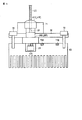
図1は、本実施形態に係るデータプロジェクタ装置10が備える電子回路の概略機能構成を示すブロック図である。
11は入出力コネクタ部であり、例えばピンジャック(RCA)タイプのビデオ入力端子、D−sub15タイプのRGB入力端子、及びUSB(Universal Serial Bus)コネクタを含む。
FIG. 1 is a block diagram illustrating a schematic functional configuration of an electronic circuit included in the
An input /
入出力コネクタ部11より入力される各種規格の画像信号は、入出力インタフェース(I/F)12、システムバスSBを介し、一般にスケーラとも称される画像変換部13に入力される。
Image signals of various standards input from the input /
画像変換部13は、入力された画像信号を投影に適した所定のフォーマットの画像信号に統一し、適宜表示用のバッファメモリであるビデオRAM14に書込んだ後に、書込んだ画像信号を読出して投影画像処理部15へ送る。
The
この際、OSD(On Screen Display)用の各種動作状態を示すシンボル等のデータも必要に応じてビデオRAM14で画像信号に重畳加工され、加工後の画像信号が読出されて投影画像処理部15へ送られる。
At this time, data such as symbols indicating various operation states for OSD (On Screen Display) is also superimposed on the image signal by the
投影画像処理部15は、送られてきた画像信号に応じて、所定のフォーマットに従ったフレームレート、例えば120[フレーム/秒]と色成分の分割数、及び表示階調数を乗算した、より高速な時分割駆動により、空間的光変調素子(SLM)であるマイクロミラー素子16を表示駆動する。
The projection
このマイクロミラー素子16は、アレイ状に配列された複数、例えばXGA(横1024画素×縦768画素)分の微小ミラーの各傾斜角度を個々に高速でオン/オフ動作することでその反射光により光像を形成する。
The
一方で、光源部17から時分割でR,G,Bの原色光が循環的に出射される。この光源部17からの原色光が、ミラー18で全反射して上記マイクロミラー素子16に照射される。
On the other hand, R, G, B primary color lights are emitted cyclically from the
そして、マイクロミラー素子16での反射光で光像が形成され、形成された光像が投影レンズユニット19を介して、投影対象となる図示しないスクリーンに投影表示される。
Then, an optical image is formed by the reflected light from the
光源部17は、具体的な光学構成については後述するが、2種類の光源、すなわち青色のレーザ光を発する半導体レーザ20と、赤色光を発するLED21とを有する。
Although the specific optical configuration will be described later, the
半導体レーザ20の発する青色のレーザ光は、ミラー22で全反射された後、ダイクロイックミラー23を透過して、カラーホイール24の周上の1点に照射される。このカラーホイール24は、モータ25により回転される。レーザ光が照射されるカラーホイール24の周上には、緑色蛍光反射板24Gと青色用拡散板24Bとが合わせてリング状となるように形成されている。
The blue laser light emitted from the
カラーホイール24の緑色蛍光反射板24Gがレーザ光の照射位置にある場合、レーザ光の照射により緑色光が励起され、励起された緑色光がカラーホイール24で反射された後、上記ダイクロイックミラー23でも反射される。その後、この緑色光は、さらにダイクロイックミラー28で反射され、インテグレータ29で輝度分布が略均一な光束とされた後にミラー30で全反射されて、上記ミラー18へ送られる。
When the green fluorescent reflector 24G of the
また、図1に示すようにカラーホイール24の青色用拡散板24Bがレーザ光の照射位置にある場合、レーザ光は該拡散板24Bで拡散されながらカラーホイール24を透過した後、ミラー26,27でそれぞれ全反射される。その後、この青色光は、上記ダイクロイックミラー28を透過し、インテグレータ29で輝度分布が略均一な光束とされた後にミラー30で全反射されて、上記ミラー18へ送られる。
Further, as shown in FIG. 1, when the
さらに、上記LED21の発した赤色光は、上記ダイクロイックミラー23を透過した後にダイクロイックミラー28で反射され、インテグレータ29で輝度分布が略均一な光束とされた後にミラー30で全反射されて、上記ミラー18へ送られる。
Further, the red light emitted from the
以上の如く、ダイクロイックミラー23は、青色光、及び赤色光を透過する一方で、緑色光を反射する分光特性を有する。
As described above, the
また、ダイクロイックミラー28は、青色光を透過する一方で、赤色光、及び緑色光を反射する分光特性を有する。
The
また、半導体レーザ20とLED21の近傍には、それぞれ2個、計4個の温度検出素子としてのサーミスタTH1〜TH4が配設される。
サーミスタTH1,TH2は、半導体レーザ20に対してその温度を検出するべく配設されたもので、サーミスタTH1が半導体レーザ20のより近位に、サーミスタTH2がサーミスタTH1よりは遠位に配置される。
Further, in the vicinity of the
The thermistors TH1 and TH2 are disposed to detect the temperature of the
同様に、サーミスタTH3,TH4は、LED21に対してその温度を検出するべく配設されたもので、サーミスタTH3がLED21のより近位に、サーミスタTH4がサーミスタTH3よりは遠位に配置される。
Similarly, the thermistors TH3 and TH4 are disposed to detect the temperature of the
なお、この図1上では、サーミスタTH3,TH4が半導体レーザ20とLED21とに挟まれた位置にあり、サーミスタTH3,TH4が本来の温度検出対象ではない半導体レーザ20の発熱の影響を受ける可能性があるようにも見える。しかしながら、詳細は後述するが、実装上は半導体レーザ20とLED21とがそれぞれ独立したヒートシンクを設けた別体のブロックとして構成されるため、温度検出手段であるサーミスタ(TH1〜TH4)が検出対象ではない熱源による影響を受ける可能性は無視できるものとする。
In FIG. 1, the thermistors TH3 and TH4 are located between the
上記光源部17の半導体レーザ20とLED21の各発光タイミング、モータ25によるカラーホイール24の回転、及びサーミスタTH1〜TH4からの温度情報の検出を投影光処理部31が統括して制御する。投影光処理部31は、投影画像処理部15から与えられる画像データのタイミングに応じて半導体レーザ20、LED21の各発光タイミング、発光輝度とカラーホイール24の回転を制御する。
The projection
上記各回路の動作すべてをCPU32が統括して制御する。このCPU32は、メインメモリ33及びプログラムメモリ34と接続される。メインメモリ33は、DRAMで構成され、CPU32のワークメモリとして機能する。プログラムメモリ34は、電気的書換可能な不揮発性メモリで構成され、動作プログラムや各種定型データ等を記憶する。
The
また上記CPU32は、操作部35からのキー操作信号に応じて各種投影動作を実行する。
この操作部35は、データプロジェクタ装置10の本体に設けられるキー操作部と、このデータプロジェクタ装置10専用の図示しないリモートコントローラの間で赤外光を受光するレーザ受光部とを含む。操作部35は、ユーザが本体のキー操作部またはリモートコントローラで操作したキーに基づくキー操作信号をCPU32へ直接出力する。
In addition, the
The
操作部35は、上記本体筐体のキー操作部、及び別体のリモートコントローラ共に、例えばフォーカス調整キー、ズーム調整キー、入力切換キー、メニューキー、カーソル(←,→,↑,↓)キー、セットキー、キャンセルキー等を備える。
The
上記CPU32はさらに、上記システムバスSBを介して音声処理部36とも接続される。音声処理部36は、PCM音源等の音源回路を備える。音声処理部36は、投影動作時に与えられる音声データをアナログ化し、スピーカ部37を駆動して拡声放音させ、あるいは必要によりビープ音等を発生させる。
The
次に、図2により主として光源部17の具体的な光学系の構成例を示す。同図は、上記光源部17周辺の構成を平面的なレイアウトで表現したものである。
Next, FIG. 2 mainly shows a specific optical system configuration example of the
ここでは、同一の発光特性を有する複数、例えば6個の半導体レーザ20A〜20Fを設け、これら半導体レーザ20A〜20Fはいずれも青色、例えば波長約450[nm]のレーザ光を発振する。
Here, a plurality of, for example, six
なお、半導体レーザ20A〜20Fは2行×3列の行列構成で配置され、本図では紙面に直交する方向が列方向であるものとして、3列の半導体レーザ20A,20B、半導体レーザ20C,20D、半導体レーザ20E,20Fを示す。
The
これら半導体レーザ20A〜20Fの発振した青色光は、レンズ41A〜41Fを介してミラー22A〜22Cで全反射され、さらにレンズ42,43を介した後に上記ダイクロイックミラー23を透過し、レンズ群44を介してカラーホイール24に照射される。
The blue light oscillated by the
カラーホイール24上では、上述した如く青色用拡散板24Bと緑色蛍光体反射板24Gとが同一円周上でリングを構成するように位置する。
On the
カラーホイール24の緑色蛍光体反射板24Gが青色光の照射位置にある場合、その照射により例えば波長約530[nm]を中心とした波長帯の緑色光が励起され、励起された緑色光がカラーホイール24で反射された後、再度レンズ群44を介してダイクロイックミラー23でも反射される。
When the green phosphor reflector 24G of the
ダイクロイックミラー23で反射した緑色光は、レンズ45を介してさらにダイクロイックミラー28で反射され、レンズ46を介してインテグレータ29で輝度分布が略均一な光束とされた後にレンズ47を介し、ミラー30で全反射されて、レンズ48を介して上記ミラー18へ送られる。
The green light reflected by the
ミラー18で全反射した緑色光は、レンズ49を介してマイクロミラー素子16に照射される。そして、その緑色光の反射光で緑色成分の光像が形成され、レンズ49、上記投影レンズユニット19を介して外部へ投射される。
The green light totally reflected by the
また、カラーホイール24の青色用拡散板24Bが青色光の照射位置にある場合、青色光は該拡散板24Bで拡散されながらカラーホイール24を透過し、背面側にあるレンズ50を介してミラー26で全反射される。
Further, when the
さらに青色光は、レンズ51を介してミラー27で全反射され、レンズ52を介した後に上記ダイクロイックミラー28を透過し、レンズ46を介してインテグレータ29で輝度分布が略均一な光束とされた後にレンズ47を介し、ミラー30で全反射されて、レンズ48を介して上記ミラー18へ送られる。
Further, the blue light is totally reflected by the
ミラー18で全反射した青色光は、レンズ49を介してマイクロミラー素子16に照射される。そして、その青色光の反射光で青色成分の光像が形成され、レンズ49、上記投影レンズユニット19を介して外部へ投射される。
The blue light totally reflected by the
一方、上記LED21は、例えば波長620[nm]の赤色光を発光する。LED21の発した赤色光は、レンズ群53を介し、上記ダイクロイックミラー23を透過した後にレンズ45を介して上記ダイクロイックミラー28で反射され、さらにレンズ46を介してインテグレータ29で輝度分布が略均一な光束とされた後にレンズ47を介し、ミラー30で全反射されて、レンズ48を介して上記ミラー18へ送られる。
On the other hand, the
ミラー18で全反射した赤色光は、レンズ49を介してマイクロミラー素子16に照射される。そして、その赤色光の反射光で赤色成分の光像が形成され、レンズ49、上記投影レンズユニット19を介して外部へ投射される。
The red light totally reflected by the
さらに本実施形態では、6個の半導体レーザ20A〜20F中で最も熱的負荷が大きいと考えられる位置にある、例えば半導体レーザ20Eまたは20Fの近傍に2個のサーミスタTH1,TH2を配設するものとする。
Furthermore, in the present embodiment, two thermistors TH1 and TH2 are disposed in the vicinity of the
図3は、データプロジェクタ装置10の筐体内に実装される構造を示す図である。同図は、データプロジェクタ装置10の筐体ケースからケース上面部を取り去った状態を示す。
図示する如く、データプロジェクタ装置10の正面に向かって、左側が主要熱源となる光源系、中央が光学系、右側が上記投影レンズユニット19を含む投影系となる。さらに、投影系と筐体ケース右側面との間の、熱的負荷が最も小さいと考えられる空間内に、各種電子回路を設けた回路基板61が設けられる。
FIG. 3 is a diagram showing a structure mounted in the housing of the
As shown in the drawing, when facing the front of the
光源系では、上記半導体レーザ20A〜20F及びレンズ41A〜41Fを設けたLD基板62に対してヒートシンク63が接続される。同様に、上記LED21を設けたLED基板64に対してヒートシンク65が接続される。これらヒートシンク63,63が隣接すると共に、ヒートシンク63を挟んでヒートシンク65とは反対側すなわちデータプロジェクタ装置10筐体の背面側には2基の冷却ファン66A,66Bが配設される。
In the light source system, a
これと合わせて、データプロジェクタ装置10筐体の正面向かって左端側、同左側側面、及び背面の同左端側には多数の開口67,68(,69(図示せず))が設けられる。
In addition to this, a large number of
冷却ファン66A,66Bにより冷却風を排出するものとする。データプロジェクタ装置10筐体の前面側及び側面から開口67,68を介して吸入された部位部の空気は、ヒートシンク65,63を通過する。
It is assumed that cooling air is discharged by the cooling
この過程で、通過する空気が上記LED基板64、LD基板62を介してLED21、半導体レーザ20A〜20Fでの発熱の一部を吸熱する。熱せられた空気は、冷却ファン66A,66Bより開口69を介してデータプロジェクタ装置10外部に排出される。
In this process, the passing air absorbs part of the heat generated by the
こうした一連の熱交換により、LED21、半導体レーザ20A〜20Fの冷却が実行され、外部に熱が排出される。
Through such a series of heat exchanges, the
なお、上記図3中で、符号70はメインフレームである。このメインフレーム70は、上記レンズ48、ミラー18、マイクロミラー素子16、レンズ49を一体に構成したボックス構造を採り、図示する如く投影レンズユニット19と連結される。
In FIG. 3,
図4は、上記LD基板62及びヒートシンク63とミラー22A〜22C周辺の構造を抽出して示す。上述した通りLD基板62とヒートシンク63とが接続され、LD基板62で生じた発熱がヒートシンク63を通過する冷却風に放射される。半導体レーザ20A〜20F自体は、LD基板62内に封入された状態となり、外部に露出しないが、各半導体レーザ20A〜20Fの出射光を位置するレンズ41A〜41Fが図示するようにLD基板62外に突出し、ミラー22に対向する。
FIG. 4 shows an extracted structure around the
図5は、LD基板62とヒートシンク63間に封入された半導体レーザ20A〜20F中の、特に半導体レーザ20E,20FとサーミスタTH1,TH2との位置関係について示す。
FIG. 5 shows a positional relationship among the
同図で、半導体レーザ20E(,20F)の発するレーザ光LBは、コリメータレンズで構成されるレンズ41E(,41F)で平行光に調整された後に、ここでは図示しないミラー22Cに向けて出射される。
In the figure, a laser beam LB emitted from a
レンズ41E(,41F)は、LD基板62上に円筒状のレンズ保持部材71により固定される。LD基板62は、ボルト72,72,‥‥により半導体レーザ20E(,20F)を挟持する状態でヒートシンク63に接続される。ヒートシンク63の半導体レーザ20E(,20F)を設けた部位には溝DTが形成される。この溝DTには、半導体レーザ20E(,20F)下面のリード配線を介してコネクタCNが収容される。
The
ヒートシンク63を通過する冷却風の方向により、下流側に位置する半導体レーザ20E,20Fは半導体レーザ20A〜20F中でも熱的負荷が最も高くなる。したがって、この半導体レーザ20E(または20F)に対して、冷却風の方向で下流側に位置するべく、半導体レーザ20E(または20F)からの距離を異ならせるようにしてサーミスタTH1,TH2を配設する。
なお、図示は省略するが、LED21に対しても、LED21からの距離を異ならせるようにしてサーミスタTH3,TH4を配設する。
Depending on the direction of the cooling air passing through the
Although illustration is omitted, the thermistors TH3 and TH4 are arranged so that the distance from the
次に上記実施形態の動作について説明する。
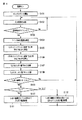
図6は、データプロジェクタ装置10の電源投入状態での処理内容を示す。この図6の処理は、プログラムメモリ34に記録された動作プログラムや固定データ等をCPU32が読出し、読出した内容をプログラムメモリ34に展開して記憶させた上でCPU32が実行する。投影光処理部31は、CPU32の制御の下に上記サーミスタTH1〜TH4を用いた温度検出やその検出結果に基づく半導体レーザ20A〜20F、LED21の駆動制御を実行する。
Next, the operation of the above embodiment will be described.
FIG. 6 shows the processing contents when the
電源投入当初、CPU32内部に設定するリングカウンタでの循環カウントを開始させる(ステップS101)。このリングカウンタは、データプロジェクタ装置10の電源が投入されている間、光源となる半導体レーザ20A〜20F、及びLED21の温度検出を行なう一定時間間隔、例えば5[秒]を循環的にカウントし続ける。
At the beginning of power-on, circulation counting is started with a ring counter set in the CPU 32 (step S101). While the
次いで入出力コネクタ部11より入力される画像に対応した光像をマイクロミラー素子16で形成し、投影レンズユニット19より投影する投影動作を実行する(ステップS102)。
Next, a projection operation is performed in which a light image corresponding to an image input from the input /
これと合わせて、上記リングカウンタのカウント値により半導体レーザ20A〜20F、及びLED21の温度検出を行なうタイミングとなったか否かを判断する(ステップS103)。
Together with this, it is determined whether or not it is time to detect the temperatures of the
ここで温度検出を行なうタイミングとはなっていないと判断した場合は、再び上記ステップS102の処理に戻り、投影動作を実行しながら温度検出を行なうタイミングとなるのを待機する。 If it is determined that it is not time to perform temperature detection, the process returns to step S102 again, and waits for the timing to perform temperature detection while performing the projection operation.
そして、リングカウンタのカウント値により温度検出を行なうタイミングとなると、ステップS103でそれを判断し、その時点で投影光処理部31がサーミスタTH1〜TH4での温度を検出する(ステップS104)。
Then, when it is time to perform temperature detection based on the count value of the ring counter, it is determined in step S103, and at that time, the projection
投影光処理部31から検出温度を取得したCPU32は、サーミスタTH1,TH2での検出温度を用いて半導体レーザ20E(,20F)のジャンクション温度TjLDを算出する(ステップS105)。
The
このとき、サーミスタTH1とサーミスタTH2の2点間の冷却能力をR11、該2点間の温度差をΔT1、半導体レーザ20E(,20F)の発熱量をQ1とすると、
R11=ΔT1/Q1 …(1)
なる式が成立する。すなわち、2点間の冷却能力R11が既知であれば、光源である半導体レーザ20E(,20F)の発熱量Q1を求めることができる。言うまでもなく該冷却能力R11は構造上容易に計算及び測定のいずれも可能であり、既知である。
At this time, assuming that the cooling capacity between two points of the thermistor TH1 and the thermistor TH2 is R11, the temperature difference between the two points is ΔT1, and the heat generation amount of the
R11 = ΔT1 / Q1 (1)
The following formula is established. That is, if the cooling capacity R11 between the two points is known, the calorific value Q1 of the
また、半導体レーザ20E(,20F)のジャンクション温度TjLDは、以下の式
TjLD=TH1+R12*Q1 …(2)
で与えられる。ここでR12は、サーミスタTH1から半導体レーザ20E(,20F)内のジャンクション(半導体接合部)までの熱抵抗値であり、上記R11と同様に既知である。
Further, the junction temperature TjLD of the
TjLD = TH1 + R12 * Q1 (2)
Given in. Here, R12 is a thermal resistance value from the thermistor TH1 to a junction (semiconductor junction) in the
したがって、CPU32はサーミスタTH1,TH2の検出結果からΔT1を求め、上記式(1)を式(2)に代入した次式
TjLD=TH1+R12*(ΔT1/R11) …(3)
により半導体レーザ20E(,20F)のジャンクション温度TjLDを取得する。
Therefore, the
TjLD = TH1 + R12 * (ΔT1 / R11) (3)
Thus, the junction temperature TjLD of the
同様にCPU32は、投影光処理部31を介して得たサーミスタTH3,TH4での検出温度を用いてLED21のジャンクション温度TjLEDを算出する(ステップS106)。
Similarly, the
このとき、サーミスタTH3とサーミスタTH4の2点間の冷却能力をR21、該2点間の温度差をΔT2、LED21の発熱量をQ2とすると、
R21=ΔT2/Q2 …(4)
なる式が成立する。すなわち、2点間の冷却能力R21が既知であれば、光源であるLED21の発熱量Q2を求めることができる。言うまでもなく該冷却能力R21も構造上容易に計算及び測定のいずれも可能であり、既知である。
At this time, assuming that the cooling capacity between two points of the thermistor TH3 and the thermistor TH4 is R21, the temperature difference between the two points is ΔT2, and the heat generation amount of the
R21 = ΔT2 / Q2 (4)
The following formula is established. That is, if the cooling capacity R21 between two points is known, the calorific value Q2 of the
また、LED21のジャンクション温度TjLEDは、以下の式
TjLED=TH3+R22*Q2 …(5)
で与えられる。ここでR22は、サーミスタTH3からLED21内のジャンクション(半導体接合部)までの熱抵抗値であり、上記R21と同様に既知である。
Further, the junction temperature TjLED of the
TjLED = TH3 + R22 * Q2 (5)
Given in. Here, R22 is the thermal resistance value from the thermistor TH3 to the junction (semiconductor junction) in the
したがって、CPU32は投影光処理部31を介して得たサーミスタTH3,TH4の検出結果からΔT2を求め、上記式(4)を式(5)に代入した次式
TjLED=TH3+R22*(ΔT2/R21) …(6)
によりLED21のジャンクション温度TjLEDを取得する。
Therefore, the
TjLED = TH3 + R22 * (ΔT2 / R21) (6)
Thus, the junction temperature TjLED of the
次いでCPU32は、上記ステップS105で得た半導体レーザ20E(,20F)のジャンクション温度TjLDを、予め用意したしきい値温度Tth1と比較参照する(ステップS107)。
Next, the
さらにCPU32は、上記ステップS106で得たLED21のジャンクション温度TjLEDを、予め用意したしきい値温度Tth2と比較参照する(ステップS108)。
Further, the
上記ステップS107,S108での各比較の結果、少なくとも一方で予め用意したしきい値を超えたジャンクション温度があるか否かにより、光源に温度異常が生じているか否かを判断する(ステップS109)。 As a result of each comparison in steps S107 and S108, it is determined whether or not a temperature abnormality has occurred in the light source based on whether or not there is a junction temperature that exceeds a threshold value prepared in advance on at least one side (step S109). .
ここでいずれのジャンクション温度TjLD,TjLEDも各しきい値を超えていない場合は、光源に温度異常は生じていないものとして、次のタイミングとなるのを待機するべく、再び上記ステップS102からの処理に戻る。 If none of the junction temperatures TjLD and TjLED exceed the threshold values, it is assumed that no temperature abnormality has occurred in the light source, and the processing from step S102 is repeated again to wait for the next timing. Return to.
また、上記ステップS109でジャンクション温度TjLD,TjLEDの少なくとも一方が予め用意したしきい値を超えていると判断した場合には、次いでしきい値を超えたジャンクション温度が1つであるか否かを判断する(ステップS110)。 If it is determined in step S109 that at least one of the junction temperatures TjLD and TjLED exceeds a threshold value prepared in advance, whether or not there is one junction temperature exceeding the threshold value is determined next. Judgment is made (step S110).
ここでしきい値を超えたジャンクション温度が1つであると判断した場合には、ジャンクション温度がしきい値を超えた側の光源、半導体レーザ20A〜20FまたはLED21の超えた度合いに合わせて、半導体レーザ20A〜20F及びLED21の双方の駆動電流を輝度バランスが崩れないように抑制させるべく調整した上で(ステップS111)、再び上記ステップS102からの処理に戻る。
If it is determined that there is one junction temperature that exceeds the threshold, the light source on the side where the junction temperature exceeds the threshold, the
また、上記ステップS110でしきい値を超えたジャンクション温度が1つではないと判断した場合には、2つのジャンクション温度が共にしきい値を超えていることとなる。したがって、2つのジャンクション温度のうち、より大きくしきい値を超えている方を選択し、その選択した側のジャンクション温度を超えている度合いに合わせて、半導体レーザ20A〜20F及びLED21の双方の駆動電流を輝度バランスが崩れないように抑制させるべく調整した上で(ステップS112)、再び上記ステップS102からの処理に戻る。
If it is determined in step S110 that the number of junction temperatures exceeding the threshold is not one, both the junction temperatures exceed the threshold. Accordingly, the higher one of the two junction temperatures that exceeds the threshold value is selected, and both the
以上詳記した如く本実施形態によれば、半導体発光素子である半導体レーザ20A〜20F及びLED21の温度をより正確に把握して、性能の劣化が生じないように適正な駆動制御を実行することが可能となる。
As described above in detail, according to the present embodiment, the temperature of the
また、上記実施形態では、特に半導体発光素子のジャンクション温度を算出して得た上で輝度を抑制するように調整を行なうようにしたため、半導体発光素子の温度異常をより正確に判断して、性能劣化を確実に阻止できる。 In the above embodiment, since the adjustment is performed so as to suppress the luminance after calculating the junction temperature of the semiconductor light emitting element in particular, it is possible to more accurately determine the temperature abnormality of the semiconductor light emitting element and perform the performance. Deterioration can be reliably prevented.
さらに上記実施形態では、半導体レーザ20A〜20FとLED21の2種類の半導体発光素子を設け、それぞれのジャンクション温度を取得した上で、より大きく適正な範囲を外れている側に基づいて双方の駆動電流を抑制するものとしたので、半導体発光素子の性能劣化を確実に防ぎながら、且つ色バランスが崩れないように制御可能となる。
Furthermore, in the said embodiment, after providing two types of semiconductor light-emitting devices,
なお、上記実施形態では、光源となる半導体発光素子として半導体レーザとLEDとを併用する場合について説明したが、本発明はこれに限らず、単独電圧子をする場合、及び複数併用して使用する場合のいずれでも適用可能である。 In the above-described embodiment, the case where the semiconductor laser and the LED are used in combination as the semiconductor light-emitting element serving as the light source has been described. Any case is applicable.
その他、本発明は上述した実施形態に限定されるものではなく、実施段階ではその要旨を逸脱しない範囲で種々に変形することが可能である。また、上述した実施形態で実行される機能は可能な限り適宜組み合わせて実施しても良い。上述した実施形態には種々の段階が含まれており、開示される複数の構成要件による適宜の組み合せにより種々の発明が抽出され得る。例えば、実施形態に示される全構成要件からいくつかの構成要件が削除されても、効果が得られるのであれば、この構成要件が削除された構成が発明として抽出され得る。 In addition, the present invention is not limited to the above-described embodiments, and various modifications can be made without departing from the scope of the invention in the implementation stage. Further, the functions executed in the above-described embodiments may be combined as appropriate as possible. The above-described embodiment includes various stages, and various inventions can be extracted by an appropriate combination of a plurality of disclosed constituent elements. For example, even if some constituent requirements are deleted from all the constituent requirements shown in the embodiment, if the effect is obtained, a configuration from which the constituent requirements are deleted can be extracted as an invention.
10…データプロジェクタ装置、11…入出力コネクタ部、12…入出力インタフェース(I/F)、13…画像変換部(スケーラ)、14…ビデオRAM、15…投影画像処理部、16…マイクロミラー素子(SLM)、17…光源部、18…ミラー、19…投影レンズユニット、20…(B発光)半導体レーザ、21…(R発光)LED、22…ミラー、23…ダイクロイックミラー、24…カラーホイール、24B…青色用拡散板、24G…緑色蛍光体反射板、25…モータ(M)、26,27…ミラー、28…ダイクロイックミラー、29…インテグレータ、30…ミラー、31…投影光処理部、32…CPU、33…メインメモリ、34…プログラムメモリ、35…操作部、36…音声処理部、37…スピーカ部、41A〜41C,42,43…レンズ、44…レンズ群、45〜52…レンズ、53…レンズ群、61…回路基板、62…LD基板、63…ヒートシンク、64…LED基板、65…ヒートシンク、66A,66B…冷却ファン、67〜69…開口、70…メインフレーム、71…レンズ保持部材、72…ボルト、CN…コネクタ、DT…溝、LB…レーザ光、SB…システムバス、TH1〜TH4…サーミスタ。
DESCRIPTION OF
Claims (9)
上記半導体発光素子に対して異なる距離に配設された複数の温度検出素子と、
上記複数の温度検出素子での各検出温度、及び上記複数の温度検出素子と上記半導体発光素子との間の温度特性から上記半導体発光素子の温度を取得する温度取得手段と、
上記温度取得手段で得た温度に基づいて上記半導体発光素子の駆動条件を制御する発光制御手段と
を具備したことを特徴とする光源装置。 A semiconductor light emitting device;
A plurality of temperature detection elements disposed at different distances from the semiconductor light emitting element;
Temperature acquisition means for acquiring the temperature of each of the plurality of temperature detection elements, and the temperature characteristics of the semiconductor light emitting element from the temperature characteristics between the plurality of temperature detection elements and the semiconductor light emitting element;
A light source device comprising light emission control means for controlling a driving condition of the semiconductor light emitting element based on the temperature obtained by the temperature acquisition means.
上記複数の半導体発光素子を冷却する冷却手段をさらに備え、
上記複数の温度検出素子は、上記複数の半導体発光素子のうち最も熱的負荷が高い半導体発光素子に対して配設されることを特徴とする請求項1又は2に記載の光源装置。 The semiconductor light emitting element is plural,
A cooling means for cooling the plurality of semiconductor light emitting elements;
3. The light source device according to claim 1, wherein the plurality of temperature detecting elements are arranged with respect to a semiconductor light emitting element having the highest thermal load among the plurality of semiconductor light emitting elements.
上記温度取得手段は、上記複数の半導体発光素子それぞれの温度を取得し、
上記発光制御手段は、上記複数の半導体発光素子それぞれの温度に応じて、各制御範囲を最も高い割合で超えている半導体発光素子に合わせて上記複数の半導体発光素子の各駆動条件を制御する
ことを特徴とする請求項3記載の光源装置。 The plurality of temperature detection elements are provided with a plurality of temperature detection elements in each of the plurality of semiconductor light emitting elements,
The temperature acquisition means acquires the temperature of each of the plurality of semiconductor light emitting elements,
The light emission control means controls each driving condition of the plurality of semiconductor light emitting elements according to the temperature of each of the plurality of semiconductor light emitting elements, in accordance with the semiconductor light emitting element exceeding the respective control range at the highest rate. The light source device according to claim 3.
上記半導体発光素子に対して異なる距離に配設された複数の温度検出素子と、
上記複数の温度検出素子での各検出温度、及び上記複数の温度検出素子と上記半導体発光素子との間の温度特性から上記半導体発光素子の温度を取得する温度取得手段と、
上記温度取得手段で得た温度に基づいて上記半導体発光素子の駆動条件を制御する発光制御手段と、
画像信号を入力する入力手段と、
上記発光制御手段での制御に基づいて上記半導体発光素子から出射される光を用い、上記入力手段で入力する画像信号に対応したカラーの光像を形成して投影する投影手段と
を具備したことを特徴とする投影装置。 A semiconductor light emitting device;
A plurality of temperature detection elements disposed at different distances from the semiconductor light emitting element;
Temperature acquisition means for acquiring the temperature of each of the plurality of temperature detection elements, and the temperature characteristics of the semiconductor light emitting element from the temperature characteristics between the plurality of temperature detection elements and the semiconductor light emitting element;
Light emission control means for controlling the driving conditions of the semiconductor light emitting element based on the temperature obtained by the temperature acquisition means;
An input means for inputting an image signal;
Projection means for forming and projecting a color light image corresponding to an image signal input by the input means, using light emitted from the semiconductor light emitting element based on the control by the light emission control means; A projection apparatus characterized by the above.
上記複数の半導体発光素子を冷却する冷却手段をさらに備え、
上記複数の温度検出素子は、上記複数の半導体発光素子のうち最も熱的負荷が高い半導体発光素子に対して配設されることを特徴とする請求項5又は6に記載の投影装置。 The semiconductor light emitting element is plural,
A cooling means for cooling the plurality of semiconductor light emitting elements;
The projection apparatus according to claim 5, wherein the plurality of temperature detection elements are arranged with respect to a semiconductor light emitting element having the highest thermal load among the plurality of semiconductor light emitting elements.
上記温度取得手段は、上記複数の半導体発光素子それぞれの温度を取得し、
上記発光制御手段は、上記複数の半導体発光素子それぞれの温度に応じて、各制御範囲を最も高い割合で超えている半導体発光素子に合わせて上記複数の半導体発光素子の各駆動条件を制御する
ことを特徴とする請求項7記載の投影装置。 The plurality of temperature detection elements are provided with a plurality of temperature detection elements in each of the plurality of semiconductor light emitting elements,
The temperature acquisition means acquires the temperature of each of the plurality of semiconductor light emitting elements,
The light emission control means controls each driving condition of the plurality of semiconductor light emitting elements according to the temperature of each of the plurality of semiconductor light emitting elements, in accordance with the semiconductor light emitting element exceeding the respective control range at the highest rate. The projection apparatus according to claim 7.
上記複数の温度検出素子での各検出温度、及び上記複数の温度検出素子と上記半導体発光素子との間の温度特性から上記半導体発光素子の温度を取得する温度取得工程と、
上記温度取得工程で得た温度に基づいて上記半導体発光素子の駆動条件を制御する発光制御工程と
を有したことを特徴とする投影方法。 A semiconductor light emitting element, a plurality of temperature detecting elements disposed at different distances from the semiconductor light emitting element, an input unit for inputting an image signal, and an image signal input by the input unit using light of the semiconductor light emitting element A projection method with a projection device including a projection unit that forms and projects a corresponding color light image,
A temperature acquisition step of acquiring the temperature of each of the plurality of temperature detection elements, and the temperature of the semiconductor light emitting element from the temperature characteristics between the plurality of temperature detection elements and the semiconductor light emitting element;
And a light emission control step of controlling a driving condition of the semiconductor light emitting element based on the temperature obtained in the temperature acquisition step.
Priority Applications (1)
| Application Number | Priority Date | Filing Date | Title |
|---|---|---|---|
| JP2010015827A JP5540732B2 (en) | 2010-01-27 | 2010-01-27 | Light source device, projection device, and projection method |
Applications Claiming Priority (1)
| Application Number | Priority Date | Filing Date | Title |
|---|---|---|---|
| JP2010015827A JP5540732B2 (en) | 2010-01-27 | 2010-01-27 | Light source device, projection device, and projection method |
Publications (3)
| Publication Number | Publication Date |
|---|---|
| JP2011154206A JP2011154206A (en) | 2011-08-11 |
| JP2011154206A5 JP2011154206A5 (en) | 2013-03-14 |
| JP5540732B2 true JP5540732B2 (en) | 2014-07-02 |
Family
ID=44540226
Family Applications (1)
| Application Number | Title | Priority Date | Filing Date |
|---|---|---|---|
| JP2010015827A Active JP5540732B2 (en) | 2010-01-27 | 2010-01-27 | Light source device, projection device, and projection method |
Country Status (1)
| Country | Link |
|---|---|
| JP (1) | JP5540732B2 (en) |
Families Citing this family (4)
| Publication number | Priority date | Publication date | Assignee | Title |
|---|---|---|---|---|
| JP6195193B2 (en) * | 2012-12-19 | 2017-09-13 | パナソニックIpマネジメント株式会社 | Light source device and projection display device |
| CN103529625B (en) * | 2013-09-18 | 2015-07-08 | 苏州佳世达光电有限公司 | Projector |
| JP2021156997A (en) * | 2020-03-26 | 2021-10-07 | セイコーエプソン株式会社 | projector |
| JP7127662B2 (en) * | 2020-03-26 | 2022-08-30 | セイコーエプソン株式会社 | Light source device and projector |
Family Cites Families (5)
| Publication number | Priority date | Publication date | Assignee | Title |
|---|---|---|---|---|
| JP4604448B2 (en) * | 2003-01-22 | 2011-01-05 | セイコーエプソン株式会社 | projector |
| JP2005121890A (en) * | 2003-10-16 | 2005-05-12 | Seiko Epson Corp | Image display device, and method for controlling temperature of light source |
| JP2006162653A (en) * | 2004-12-02 | 2006-06-22 | Olympus Corp | Light source apparatus and projector |
| JP2008124303A (en) * | 2006-11-14 | 2008-05-29 | Seiko Epson Corp | Drive controller of semiconductor light-emitting element, projection display device having drive controller, and method of them |
| JP4525767B2 (en) * | 2008-02-14 | 2010-08-18 | ソニー株式会社 | Lighting device and display device |
-
2010
- 2010-01-27 JP JP2010015827A patent/JP5540732B2/en active Active
Also Published As
| Publication number | Publication date |
|---|---|
| JP2011154206A (en) | 2011-08-11 |
Similar Documents
| Publication | Publication Date | Title |
|---|---|---|
| TWI420225B (en) | Light source unit and projector | |
| JP5713168B2 (en) | Light source unit and projector | |
| JP4936091B2 (en) | Light source unit and projector | |
| JP5488908B2 (en) | projector | |
| JP5500339B2 (en) | Light source device and projector | |
| JP5206814B2 (en) | Cooling device, cooling control method and program | |
| JP6172538B2 (en) | Electronic device, projection device, and method of manufacturing electronic device | |
| KR101490015B1 (en) | Light source unit and projector | |
| JP6202346B2 (en) | Heat dissipation device, light source device and projection device | |
| JP2010217566A (en) | Light emitting device, light source device, and projector using the light source device | |
| JP2012199453A (en) | Cooling device and projector | |
| JP5862951B2 (en) | Light source device and projector | |
| JP2015185551A (en) | Cooling device, light source device and projector | |
| JP5804316B2 (en) | projector | |
| JP6260819B2 (en) | Light source device and projector | |
| JP5540732B2 (en) | Light source device, projection device, and projection method | |
| JP7049574B2 (en) | Cooling device, light source device and projection device | |
| JP2021122138A (en) | Abnormality detection device, projection device, abnormality detection method and program | |
| JP5787133B2 (en) | Light source unit and projector | |
| JP2011133789A (en) | Light source apparatus and projector | |
| JP2015052791A (en) | Light source device and projector | |
| JP6820703B2 (en) | Light source device and projection device | |
| JP2012053279A (en) | Color image forming apparatus, color image forming method, and projector including the color image forming apparatus | |
| JP5408494B2 (en) | Projector, projector light source initial drive voltage setting method, and projector light source drive voltage setting method | |
| JP5811112B2 (en) | Cooling device, projector, cooling control method and program |
Legal Events
| Date | Code | Title | Description |
|---|---|---|---|
| A521 | Written amendment |
Free format text: JAPANESE INTERMEDIATE CODE: A523 Effective date: 20130124 |
|
| A621 | Written request for application examination |
Free format text: JAPANESE INTERMEDIATE CODE: A621 Effective date: 20130124 |
|
| A977 | Report on retrieval |
Free format text: JAPANESE INTERMEDIATE CODE: A971007 Effective date: 20131021 |
|
| A131 | Notification of reasons for refusal |
Free format text: JAPANESE INTERMEDIATE CODE: A131 Effective date: 20131029 |
|
| A521 | Written amendment |
Free format text: JAPANESE INTERMEDIATE CODE: A523 Effective date: 20131219 |
|
| A131 | Notification of reasons for refusal |
Free format text: JAPANESE INTERMEDIATE CODE: A131 Effective date: 20140121 |
|
| A521 | Written amendment |
Free format text: JAPANESE INTERMEDIATE CODE: A523 Effective date: 20140317 |
|
| TRDD | Decision of grant or rejection written | ||
| A01 | Written decision to grant a patent or to grant a registration (utility model) |
Free format text: JAPANESE INTERMEDIATE CODE: A01 Effective date: 20140408 |
|
| A61 | First payment of annual fees (during grant procedure) |
Free format text: JAPANESE INTERMEDIATE CODE: A61 Effective date: 20140421 |
|
| R150 | Certificate of patent or registration of utility model |
Ref document number: 5540732 Country of ref document: JP Free format text: JAPANESE INTERMEDIATE CODE: R150 |