JP5529577B2 - Electromechanical transducer and method for manufacturing the same - Google Patents
Electromechanical transducer and method for manufacturing the same Download PDFInfo
- Publication number
- JP5529577B2 JP5529577B2 JP2010029599A JP2010029599A JP5529577B2 JP 5529577 B2 JP5529577 B2 JP 5529577B2 JP 2010029599 A JP2010029599 A JP 2010029599A JP 2010029599 A JP2010029599 A JP 2010029599A JP 5529577 B2 JP5529577 B2 JP 5529577B2
- Authority
- JP
- Japan
- Prior art keywords
- elements
- electromechanical transducer
- electrode
- substrate
- manufacturing
- Prior art date
- Legal status (The legal status is an assumption and is not a legal conclusion. Google has not performed a legal analysis and makes no representation as to the accuracy of the status listed.)
- Active
Links
Images


Description
本発明は、超音波などの弾性波の受信及び送信のうちの少なくとも一方を行う容量型超音波変換装置などの電気機械変換装置及びその作製方法に関するものであり、高感度な二次元センサデバイスなどの実現に適用可能な技術に関する。 The present invention relates to an electromechanical transducer such as a capacitive ultrasonic transducer that performs at least one of reception and transmission of elastic waves such as ultrasonic waves, and a method for manufacturing the electromechanical transducer, such as a highly sensitive two-dimensional sensor device. It is related with the technology applicable to realization.
近年、マイクロマシンニング工程を用いて作製される容量型電気機械変換装置が盛んに研究されている。通常の容量型電気機械変換装置は、下部電極と間隔を隔てて支持された振動膜と、振動膜の表面に配設される上部電極とを含むセルを有する。これは、例えば、容量型超音波変換装置(CMUT:Capacitive-Micromachined-Ultrasonic-Transducer)などとして用いられる。一般的に、CMUTは、複数(通常100〜3000個程度)のセルを1エレメント(1素子)として、200〜4000程度のエレメントから構成され、CMUT自体は数mm程度のサイズである。CMUTは、軽量の振動膜を用いて超音波の送信や受信を行い、液中や空気中でも優れた広帯域特性を持つものが容易に得られる。このCMUTを利用すると、従来の医療診断より高精度な診断が可能となるため、有望な技術として注目されつつある。 In recent years, a capacitive electromechanical transducer manufactured using a micromachining process has been actively studied. A typical capacitive electromechanical transducer has a cell including a vibrating membrane supported with a distance from a lower electrode, and an upper electrode disposed on the surface of the vibrating membrane. This is used as, for example, a capacitive ultrasonic transducer (CMUT: Capacitive-Micromachined-Ultrasonic-Transducer). In general, a CMUT is composed of about 200 to 4000 elements, with a plurality of (usually about 100 to 3000) cells as one element (one element), and the CMUT itself is about several mm in size. The CMUT transmits and receives ultrasonic waves using a lightweight vibrating membrane, and can easily obtain a broadband characteristic having excellent broadband characteristics even in liquid or air. When this CMUT is used, diagnosis with higher accuracy than conventional medical diagnosis is possible, and therefore, it is attracting attention as a promising technology.
容量型電気機械変換装置の動作原理について説明する。超音波などの弾性波を送信する際には、下部電極と上部電極との間に、DC電圧に微小なAC電圧を重畳して印加する。これにより、振動膜が振動し弾性波が発生する。弾性波を受信する際には、振動膜が弾性波により変形するので、変形に伴う下部電極と上部電極との間の容量変化により弾性波の信号を検出する。一般に、超音波、音波などの送信や受信を行う為には、複数のエレメントをアレイ化した電気機械変換装置が使用されている。 The operation principle of the capacitive electromechanical transducer will be described. When transmitting an elastic wave such as an ultrasonic wave, a minute AC voltage is superimposed on the DC voltage and applied between the lower electrode and the upper electrode. Thereby, the vibration film vibrates and an elastic wave is generated. When the elastic wave is received, the vibration film is deformed by the elastic wave, and the elastic wave signal is detected by the change in capacitance between the lower electrode and the upper electrode accompanying the deformation. In general, an electromechanical transducer in which a plurality of elements are arrayed is used to transmit and receive ultrasonic waves and sound waves.
電気機械変換装置のアレイ化に係わる技術として、圧電体と回路基板を結合させたものが提案されている(特許文献1参照)また、センサアレイと集積回路モジュールを備えた電子素子アレイのアセンブリの提案がある(特許文献2参照)。 As a technique related to arraying of electromechanical transducers, a technique in which a piezoelectric body and a circuit board are combined is proposed (see Patent Document 1). Also, an assembly of an electronic element array including a sensor array and an integrated circuit module is proposed. There is a proposal (see Patent Document 2).
しかしながら、所望の周波数帯域で所望の感度を持つ二次元容量型電気機械変換装置を歩留まり良く作製する為には、上述のアレイ化技術では充分とは言い難い。 However, in order to manufacture a two-dimensional capacitive electromechanical transducer having a desired sensitivity in a desired frequency band with a high yield, the above-described array technology is not sufficient.
上記課題に鑑み、第1の電極と、前記第1の電極と間隙を挟んで設けられた第2の電極と、から少なくとも構成されるセルを含むエレメントを複数個有する本発明の電気機械変換装置は次の特徴を有する。すなわち、前記複数のエレメントは、複数の処理回路が形成された集積回路基板上のそれぞれ対応する処理回路に対して、互いに分離して独立的に配置される。また、各エレメント毎に信号の入出力ができる様に、対応する前記複数の処理回路とそれぞれ機械的及び電気的に結合される。 In view of the above problems, the electromechanical transducer according to the present invention has a plurality of elements each including a cell composed of at least a first electrode and a second electrode provided with a gap between the first electrode and the first electrode. Has the following characteristics. That is, the plurality of elements are arranged separately from each other and independently with respect to the corresponding processing circuits on the integrated circuit substrate on which the plurality of processing circuits are formed. In addition, it is mechanically and electrically coupled to the corresponding processing circuits so that signals can be input and output for each element.
また、上記課題に鑑み、第1の電極と、前記第1の電極と間隙を挟んで設けられた第2の電極と、から少なくとも構成されるセルを含むエレメントを複数個有する本発明の電気機械変換装置の作製方法は次の工程を含むことを特徴とする。基板に複数のエレメントを多面配置して作製する作製工程。前記基板に作製された複数のエレメントのうちから良好なエレメントを選択して切り出し、複数の処理回路が形成された集積回路基板上のそれぞれ対応する処理回路に対して、互いに分離して独立的に配置する配置工程。前記複数のエレメントを、各エレメント毎に信号の入出力ができる様に、対応する前記複数の処理回路とそれぞれ機械的及び電気的に結合する結合工程。 Further, in view of the above problems, the electric machine of the present invention has a plurality of elements including at least a cell composed of the first electrode and the second electrode provided with a gap between the first electrode and the first electrode. The method for manufacturing the conversion device includes the following steps. A production process in which a plurality of elements are arranged on a substrate in multiple faces. A good element is selected and cut out from the plurality of elements fabricated on the substrate, and the corresponding processing circuits on the integrated circuit board on which the plurality of processing circuits are formed are separated from each other independently. Arrangement process to arrange. A coupling step of mechanically and electrically coupling the plurality of elements to the corresponding processing circuits so that signals can be input and output for each element.
本発明によれば、基板に作製された複数のチップ(エレメント)のうちから、予め検査された良品チップを選択して切り出し、集積回路基板上の対応する処理回路に接続することができる。従って、所望の周波数帯域で良好な感度を有する二次元容量型電気機械変換装置などを無欠陥ないし歩留まり良く作製することが可能となる。 According to the present invention, a non-defective chip that has been inspected in advance can be selected from a plurality of chips (elements) fabricated on a substrate and connected to a corresponding processing circuit on an integrated circuit substrate. Accordingly, it is possible to manufacture a two-dimensional capacitive electromechanical transducer having good sensitivity in a desired frequency band with no defect or high yield.
以下、本発明の実施形態について説明する。本発明では、基板に作製された複数のチップ(エレメント)のうちから良好なチップを選択して切り出し、集積回路基板上の対応する処理回路に接続して電気機械変換装置を構成しようとするものである。この考え方に基づき、本発明の電気機械変換装置及びその作製方法の基本的な形態は、上述した様な構成を有する。この基本的な形態を基に、次に述べる様な実施形態が可能である。 Hereinafter, embodiments of the present invention will be described. In the present invention, a good chip is selected from a plurality of chips (elements) fabricated on a substrate, cut out, and connected to a corresponding processing circuit on an integrated circuit substrate to constitute an electromechanical converter. It is. Based on this concept, the basic form of the electromechanical transducer of the present invention and the manufacturing method thereof has the configuration as described above. On the basis of this basic form, the following embodiments are possible.
前記複数のエレメント(素子)は、互いに異なった共振周波数特性を持つ複数のエレメントを含むことができる。一般に、超音波画像診断では、対象とする被検体物により検出する周波数が異なり、より広帯域が要求される。共振周波数を決定するのは、CMUTなどを構成するキャビティの大きさ、電極間のギャップ、メンブレン膜材料の物性値(ヤング率、ポアソン比)や膜厚である。このことから、同一基板上の構成に、異なる共振周波数を持たせる為にはキャビティ径を変える方法が簡易的である。しかしながら、この方法では、一定の面積内において、それぞれのキャビティ径による送受信構造の総合面積を異ならせて配置するか、非効率的な配置を取らざるを得ない。上記の如く異なった共振周波数特性を持つ複数のエレメントを含む構成は、こうした課題を解決して上記要求に答えるものである。この構成によれば、異なった周波数帯域に感度特性を持つ複数種のセンサチップを同じキャビティ径でメンブレン膜(振動膜)の硬さ(物性値におけるヤング率に相当する)などを変えて作製できる。こうして、所望の周波数帯域でより高感度な二次元容量型電気機械変換装置などを無欠陥ないし歩留まり良く作製することが可能となる。 The plurality of elements (elements) may include a plurality of elements having different resonance frequency characteristics. In general, in ultrasonic image diagnosis, a frequency to be detected differs depending on a target object, and a wider band is required. The resonance frequency is determined by the size of the cavity constituting the CMUT or the like, the gap between the electrodes, the physical property values (Young's modulus, Poisson's ratio) and the film thickness of the membrane film material. For this reason, a method of changing the cavity diameter is simple in order to have different resonance frequencies on the same substrate. However, in this method, it is unavoidable to arrange the transmission / reception structures depending on the respective cavity diameters within a certain area, or to arrange them inefficiently. The configuration including a plurality of elements having different resonance frequency characteristics as described above solves these problems and meets the above requirements. According to this configuration, it is possible to produce a plurality of types of sensor chips having sensitivity characteristics in different frequency bands by changing the hardness of the membrane film (vibrating film) (corresponding to the Young's modulus in physical properties) with the same cavity diameter. . In this way, it is possible to manufacture a two-dimensional capacitive electromechanical transducer having higher sensitivity in a desired frequency band with no defect or high yield.
また、複数のエレメントを、集積回路基板上のそれぞれ対応する処理回路に直結させて接続することができる。一般に、二次元化に伴ない電気実装の負荷が増大し、ワイヤーボンディングなどの手段では高密度化ができない。更に、CMUTなどにおいては超音波による振動信号を容量値の変化に変換する為、デバイスが持つ寄生容量が大きいと、それだけ感度特性を悪化させることになり、寄生容量の低減は大きな課題である。上記集積回路基板上にて直結させる構造は、こうした課題を解決するものである。 In addition, the plurality of elements can be directly connected to the corresponding processing circuits on the integrated circuit substrate. In general, the load of electrical mounting increases with the two-dimensionalization, and the density cannot be increased by means such as wire bonding. Further, in CMUT and the like, vibration signals generated by ultrasonic waves are converted into changes in capacitance value. Therefore, if the parasitic capacitance of the device is large, the sensitivity characteristic is deteriorated accordingly, and the reduction of parasitic capacitance is a big problem. The structure directly connected on the integrated circuit board solves such a problem.
以下、本発明の実施形態を図を参照しながら説明する。
(実施形態1)
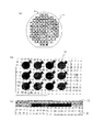
本発明の実施形態1を説明する。図1に示す本実施形態の電気機械変換装置は、少なくとも1つのセルを含むエレメントであるセンサチップを複数個有する。各セルは、第1の電極である下部電極とキャビティ(間隙)を隔てて対向して設けられた第2の電極である上部電極とを含む。エレメントは、1つ以上の前記セルからなり、複数のセルを有する場合は、エレメント内の各セルは電気的に並列に接続されている。センサチップは、共振周波数が1MHzを持つセンサチップ1、共振周波数が5MHzを持つセンサチップ2、共振周波数が10MHzを持つセンサチップ3を含む。これらのセンサチップは、バンプ4により電気実装されて集積回路基板5と電気的に接続されている。また、絶縁材料のアンダーフィル6により、センサチップ1〜3と集積回路基板5との間の隙間及びセンサチップ1〜3間の隙間が充填されており、その上層に共通上配線7がインクジェット描画機により直接描画されてセルの上部電極を共通電極としている。複数のセンサチップ1〜3は互いに分離して独立的に配置されて、それぞれ、集積回路基板5上の対応するエレメント単位の処理回路にバンプ4で直結されているので、電気機械変換装置は寄生容量を殆ど持たない。
Embodiments of the present invention will be described below with reference to the drawings.
(Embodiment 1)
本実施形態の電気機械変換装置作製方法を説明する。図2(a)は、本実施形態の作製に用いるセンサチップ9のシリコン基板8上での配置を示す上面図、図2(b)は、センサチップ9の各セルのキャビティ11形成用の犠牲層の形成工程を示す上面図である。また、図2(c)は、図2(b)のセルとなる部分のA−A’断面図である。図2(a)に示す様に、比抵抗値0.02Ω・cmの4インチシリコン基板8に、2mm角のエレメント単位のセンサチップ9を多面配置して作製する。この作製は、以下のサーフェイス型MEMS工法に従って行われる。図2(b)と図2(c)のキャビティ11となる犠牲層の形成工程では、クロム膜10を200nm厚シリコン基板8上に成膜し、フォトリソにて、25μmΦのキャビティ11となる様に犠牲層のパターニングを行う。そして、図2(c)に示す様に、シリコン基板8にプラズマCVD装置にて、メンブレン膜(振動膜)となるSiN膜12を400nm厚成膜する。この時、成膜パラメータとして、SiH4ガス流量、NH3ガス流量、N2ガス流量、高周波(RF)電源の周波数、RFパワー、基板温度によりSiN膜12の物性値が制御可能である。ヤング率は、SiとNの成分比率においてSiが多くなると低下する。従って、SiH4ガスとNH3ガスの流量比によりヤング率の制御が可能となる。本実施形態では、シリコン基板8自体を下部電極として用いる。また、メンブレン膜となるSiN膜12のヤング率を100GPa、170GPa、240GPaとして、センサチップの各共振周波数を1MHz、5MHz、10MHzとなる様にした。すなわち、図3に示すレシピA、B、Cで、3枚のウェーハ基板8にそれぞれ異なるSiN膜12の成膜を行った。
A method for manufacturing the electromechanical transducer according to this embodiment will be described. 2A is a top view showing the arrangement of the sensor chip 9 used for the fabrication of this embodiment on the
図4(a)、(b)はキャビティ形成工程を示す。ここでは、キャビティ11形成用の犠牲層であるパターニングされたクロム膜10上に成膜されたSiN膜12の一部に、ドライエッチングにて、各クロム膜10に通じる微細なエッチング孔13を開ける。そして、エッチャントとしての硝酸セリウムアンモニウム液に基板を浸漬してクロム犠牲層10をエッチング除去し、水洗と乾燥を経てキャビティ(空洞部)14を形成する。次に、図5(a)、(b)は上部電極形成工程を示す。ここでは、基板上にスパッタにてアルミ膜を400nm厚成膜し、エッチング孔13の封止16と上部電極パターン17を形成する。
4A and 4B show the cavity forming process. Here, fine etching holes 13 communicating with each
図6(a)は電気実装を行う為のUBM(Under Bump Metal)層形成工程を示す。ここでは、ウェーハ(基板)8の裏面に、ステンシルマスク18に形成された孔を各センサチップ9と対応させて該ステンシルマスク18をアライメントセットする。そして、センサチップ9と対応したウェーハ裏面の各部分に、チタン/ニッケル/金(=UBM層)19を連続成膜で形成する。こうして、基板8に複数のエレメント9を多面配置して作製する作製工程が実行される。
FIG. 6A shows a UBM (Under Bump Metal) layer forming process for electrical mounting. Here, the
その後、ウェーハ上に複数配置されたセンサチップ9について、上部電極と下電極間の短絡不良やクロム除去の不良などを検査する。そして、全てのセルが良品であるセンサチップ9をダイシングで切り出し選別した。ここでは、約80%の良品のセンサチップ(エレメント)9が選別された。図6(b)は電気実装終了時の形態を示す。この電気実装工程では、良品のチップ9のUBM層19にクリーム半田を印刷で転写し、リフロー炉に通してバンプ4を形成する。一方、エレメント単位に処理回路20が複数配置された集積回路基板5側のUBM層21に、クリーム半田を印刷する。そして、フリップチップボンダーにて、対応する処理回路20のUBM層21にセンサチップ9をアライメント実装した後に、リフロー炉に通して電気的接続を完了させる。更に、毛細管現象を利用して、センサチップ9と集積回路基板5との間及び複数のエレメント間にアンダーフィル材6を充填し、加熱硬化して機械的結合を完了させる。以上の様にして、基板8に作製された複数のエレメント9のうちから良好なエレメントを選択して切り出し、複数の処理回路20が形成された集積回路基板5上のそれぞれ対応する処理回路に対して、互いに分離して独立的に配置する配置工程が実行される。また、複数のエレメント9を、エレメント毎に信号の入出力ができる様に、対応する複数の処理回路20とそれぞれ機械的及び電気的に結合する結合工程が実行される。
Thereafter, a plurality of sensor chips 9 arranged on the wafer are inspected for a short circuit failure between the upper electrode and the lower electrode, a chromium removal failure, and the like. And the sensor chip 9 in which all the cells are non-defective was cut out and selected by dicing. Here, about 80% of non-defective sensor chips (elements) 9 were selected. FIG. 6B shows a form at the end of electrical mounting. In this electrical mounting step, the cream solder is transferred to the
図6(c)は最終工程を示す。ここでは、電気機械変換装置の各セルの上部電極を共通電極とする為に、インクジェット描画機22にて導電ペースト23を吐出し、各センサチップ9の上部電極パターン17と電気的接続が取れる様に共通上配線7を描画する。そして、共通上配線7を加熱硬化して電気実装工程を完了させる。こうして、前記充填された絶縁材料6の表面に、複数のエレメント9の各セルの一方の電極を共通電極とする配線をインクジェット描画により形成することができる。こうして作製された本実施形態の二次元容量型電気機械変換装置の受信特性を、校正されたハイドロフォンにより、ひまし油の満たされた中で計測した。その結果、図7(a)に示す個別の周波数帯域を持つセンサチップ9を含む容量型電気機械変換装置の周波数帯域として図7(b)に示す広帯域化された周波数帯域が計測された。
FIG. 6C shows the final process. Here, in order to use the upper electrode of each cell of the electromechanical conversion device as a common electrode, the
(実施形態2)
次に、本発明の実施形態2を説明する。本実施形態は、共振周波数特性を更に近接させて制御する形態である。本実施形態の電気機械変換装置では、それぞれのセンサチップの共振周波数が1MHz、2MHz、3MHzである。こうした共振周波数の実現には、ヤング率が同じメンブレン膜(振動膜)の膜厚を変化させる手法が有効である。本実施形態では、ヤング率が130GPaの<100>単結晶シリコンを各セルのメンブレン膜とする為に、シリコン直接接合型MEMS工法に従って電気機械変換装置を作製する。
(Embodiment 2)
Next,
本実施形態の作製方法を説明する。図8(a)は、本実施形態の作製に用いるセンサチップ(エレメント)25のシリコン基板24上での多面配置を示す上面図、図8(b)は、センサチップ25の酸化膜26の形成工程を示す断面図である。また、図8(c)は、センサチップ25の酸化膜26のエッチング工程を示す断面図、図8(d)は、センサチップ25におけるウェーハ接合工程を示す断面図、図8(e)は、センサチップ25のメンブレン膜31の形成工程を示す断面図である。ここでは、図8(a)に示す様に、比抵抗値0.02Ω・cmの4インチシリコン基板24に、2mm角のエレメント単位のセンサチップ25を多面配置して作製を行う。この作製は、以下の接合型MEMS工法に従って行われる。図8(b)の酸化膜形成工程では、熱酸化炉におけるパイロジェニック酸化(1000℃、90分)で200nm厚の酸化膜26をシリコン基板24に形成する。図8(c)の酸化膜エッチング工程では、キャビティとなる部分27の酸化膜26をCF4ガスによるRIEエッチングで除去する。図8(d)のウェーハ接合工程は、結晶方位<100>のシリコン活性層を有するSOI基板28との接合工程であり、事前にそれぞれの基板24、28を洗浄し、N2プラズマに10分曝して活性化した面を真空接合装置にて約0.4Paの雰囲気で貼り合わせる。その後、1100℃で2時間の加熱を行い2枚のシリコン基板24、28の接合を完了させる。ここで、シリコン活性層29の膜厚が400nm、800nm、1100nmと異なる3種類のSOI基板28を使用して接合を行った。
A manufacturing method of this embodiment will be described. FIG. 8A is a top view showing a multi-face arrangement on the
図8(e)の形成工程では、その後、SOI基板28の裏面から、バックグラインダーとKOH液を用いてBOX(埋め込み酸化膜)層30まで除去し、最後にフッ酸にてBOX層30を除去して単結晶シリコンのメンブレン膜(振動膜)31を形成する。更に、実施形態1と同様に、電気実装の為のUBM層を形成し、検査を行い、3種類の共振周波数を持つ約60%の良品チップを用いて二次元容量型電気機械変換装置を作製した。同じく、受信特性として、図9に示す様な5MHz以下の帯域で高感度な受信特性を確認した。この様に比較的低周波の帯域に高感度な共振周波数特性を有する電気機械変換装置は、乳がん等の早期発見のために使用されるセンサデバイスとして有効とされている。本実施形態によれば、目的に適合したセンサデバイスをエレメント欠陥無くないし歩留まり良く作製することができる。
8E, after that, from the back surface of the
尚、上記実施形態ではシリコン基板を用いてセンサチップを作製したが、これに限ることなく他の材料(ガラス基板など)を用いたチップでも構わない。また、電気実装においてバンプ接続を用いたが、導電性接着剤、異方性導電フィルムなどを用いる実装技術でも採用可能である。更に、インクジェット描画装置による上配線形成法は、比較的段差のある面においても断切れすることなく配線を容易に形成でき、成膜装置やフォトリソなどの大型装置を用いることなく配線形成が可能であるので、非常に有効な手法である。 In the above embodiment, the sensor chip is manufactured using the silicon substrate. However, the present invention is not limited to this, and a chip using another material (such as a glass substrate) may be used. Moreover, although bump connection was used in electrical mounting, it is also possible to employ mounting technology using a conductive adhesive, an anisotropic conductive film, or the like. Furthermore, the upper wiring forming method using an ink jet drawing apparatus can easily form wiring without breaking even on a relatively stepped surface, and wiring can be formed without using a large-scale apparatus such as a film forming apparatus or photolithography. This is a very effective method.
1、2、3、9、25…エレメント(センサチップ)、5…集積回路基板、8、24…基板(シリコン基板)、12、31…メンブレン膜(振動膜)、14、27…キャビティ(空洞部)、17…上部電極、20…処理回路 1, 2, 3, 9, 25 ... element (sensor chip), 5 ... integrated circuit substrate, 8, 24 ... substrate (silicon substrate), 12, 31 ... membrane membrane (vibrating membrane), 14, 27 ... cavity (cavity) Part), 17 ... upper electrode, 20 ... processing circuit
Claims (6)
前記複数のエレメントは、エレメント毎に互いに分離され、それぞれ独立して集積回路基板上に配置されているとともに、前記エレメント間には絶縁材料が充填されており、
前記複数のエレメント間の前記第2の電極同士は、前記絶縁材料上に設けられた配線により電気的に接続されており、
前記複数のエレメントのそれぞれと、前記集積回路基板に設けられた複数の処理回路のそれぞれと、は機械的及び電気的に結合されていることを特徴とする電気機械変換装置。 An electromechanical transducer having a plurality of elements including at least a cell composed of a first electrode and a vibrating membrane including a second electrode provided with a gap between the first electrode,
The plurality of elements are separated from one another for each element, and are arranged independently on an integrated circuit board , and an insulating material is filled between the elements ,
The second electrodes between the plurality of elements are electrically connected by wiring provided on the insulating material,
Respectively, respectively, the electromechanical transducer, characterized in that it is mechanically and electrically coupled a plurality of processing circuits provided in the integrated circuit board of the plurality of elements.
前記複数のエレメントを基板上に作製する作製工程と、
前記基板に作製された複数のエレメントのうちから所望のエレメントを切り出す工程と、
複数の処理回路が形成された集積回路基板上に、切り出されたエレメントのそれぞれを互いに分離して独立的に配置する配置工程と、
前記エレメント間に絶縁材料を充填する工程と、
前記絶縁材料上に、前記エレメント間の前記第2の電極同士を電気的に接続する配線を形成する工程と、
を備え、
前記複数のエレメントのそれぞれと、前記複数の処理回路のそれぞれと、は機械的及び電気的に結合することを特徴とする電気機械変換装置の作製方法。 A method of manufacturing an electromechanical transducer having a plurality of elements including at least a cell composed of a first electrode and a vibrating membrane including a second electrode provided with a gap between the first electrode and the first electrode. There,
A producing step of producing a plurality of elements on a substrate,
A switching Ride to process a desired element from among a plurality of elements made in said substrate,
An arrangement step of independently disposing each of the cut out elements on an integrated circuit substrate on which a plurality of processing circuits are formed;
Filling an insulating material between the elements;
Forming a wiring electrically connecting the second electrodes between the elements on the insulating material;
With
Wherein each a plurality of elements, respectively of said plurality of processing circuits, the mechanical and manufacturing method of electromechanical transducer according to claim electrically coupled to Turkey.
Priority Applications (1)
| Application Number | Priority Date | Filing Date | Title |
|---|---|---|---|
| JP2010029599A JP5529577B2 (en) | 2010-02-14 | 2010-02-14 | Electromechanical transducer and method for manufacturing the same |
Applications Claiming Priority (1)
| Application Number | Priority Date | Filing Date | Title |
|---|---|---|---|
| JP2010029599A JP5529577B2 (en) | 2010-02-14 | 2010-02-14 | Electromechanical transducer and method for manufacturing the same |
Publications (2)
| Publication Number | Publication Date |
|---|---|
| JP2011166633A JP2011166633A (en) | 2011-08-25 |
| JP5529577B2 true JP5529577B2 (en) | 2014-06-25 |
Family
ID=44596755
Family Applications (1)
| Application Number | Title | Priority Date | Filing Date |
|---|---|---|---|
| JP2010029599A Active JP5529577B2 (en) | 2010-02-14 | 2010-02-14 | Electromechanical transducer and method for manufacturing the same |
Country Status (1)
| Country | Link |
|---|---|
| JP (1) | JP5529577B2 (en) |
Families Citing this family (4)
| Publication number | Priority date | Publication date | Assignee | Title |
|---|---|---|---|---|
| US10736607B2 (en) | 2013-11-15 | 2020-08-11 | Koninklijke Philips N.V. | Integrated circuit array and method for manufacturing an array of integrated circuits |
| JP6399803B2 (en) * | 2014-05-14 | 2018-10-03 | キヤノン株式会社 | Force sensor and gripping device |
| CN112075090B (en) * | 2018-05-03 | 2022-10-14 | 蝴蝶网络有限公司 | Pressure port for ultrasonic transducer on CMOS sensor |
| EP3680211B1 (en) | 2019-01-10 | 2024-03-06 | TE Connectivity Solutions GmbH | Sensor unit and method of interconnecting a substrate and a carrier |
Family Cites Families (5)
| Publication number | Priority date | Publication date | Assignee | Title |
|---|---|---|---|---|
| JPS56154899A (en) * | 1980-04-30 | 1981-11-30 | Toshiba Corp | Array type ultrasonic probe |
| JP4252441B2 (en) * | 2003-12-25 | 2009-04-08 | パナソニック株式会社 | Ultrasonic probe |
| US7923894B2 (en) * | 2006-12-05 | 2011-04-12 | Panasonic Corporation | Actuator, image projection apparatus and production method for actuator |
| JP5108100B2 (en) * | 2008-06-17 | 2012-12-26 | 株式会社日立製作所 | Manufacturing method of semiconductor device |
| JP5594986B2 (en) * | 2008-06-24 | 2014-09-24 | キヤノン株式会社 | Method of manufacturing electromechanical transducer and electromechanical transducer |
-
2010
- 2010-02-14 JP JP2010029599A patent/JP5529577B2/en active Active
Also Published As
| Publication number | Publication date |
|---|---|
| JP2011166633A (en) | 2011-08-25 |
Similar Documents
| Publication | Publication Date | Title |
|---|---|---|
| US8466522B2 (en) | Element array, electromechanical conversion device, and process for producing the same | |
| JP7026111B2 (en) | Electrical Contact Devices Arrangement for Micromachined Ultrasonic Transducers | |
| KR101206030B1 (en) | RF module, multi RF module, and method of fabricating thereof | |
| US7489593B2 (en) | Electrostatic membranes for sensors, ultrasonic transducers incorporating such membranes, and manufacturing methods therefor | |
| US9511996B2 (en) | Methods of forming semiconductor structures including MEMS devices and integrated circuits on common sides of substrates, and related structures and devices | |
| US8402831B2 (en) | Monolithic integrated CMUTs fabricated by low-temperature wafer bonding | |
| US8371018B2 (en) | Electromechanical transducer and manufacturing method therefor | |
| CN108405291A (en) | Energy converter and transducer array | |
| US9143877B2 (en) | Electromechanical transducer device and method of making the same | |
| US10669152B2 (en) | Device arrangement | |
| US9481566B2 (en) | Methods of forming semiconductor structures including MEMS devices and integrated circuits on opposing sides of substrates, and related structures and devices | |
| KR101761819B1 (en) | Ultrasonic transducer and method of manufacturing the sames | |
| JP5529577B2 (en) | Electromechanical transducer and method for manufacturing the same | |
| KR101526254B1 (en) | Vibration power generation device and method for manufacturing same | |
| JP2010098454A (en) | Mechanoelectric transducer element | |
| US7164222B2 (en) | Film bulk acoustic resonator (FBAR) with high thermal conductivity | |
| WO2020134665A1 (en) | Control circuit, integration method for acoustic wave filter, and integration structure | |
| WO2021184138A1 (en) | Preparation process for thin film bulk acoustic wave resonator provided with flexible insulating substrate and circuit thereof | |
| US20180111824A1 (en) | Semiconductor structure and manufacturing method thereof | |
| JP5807226B2 (en) | Vibration element and method for manufacturing vibration element | |
| KR102359155B1 (en) | Hybrid ultrasound prove array and method of manufacturing the same | |
| US20220280971A1 (en) | Ultrasound transducer manufacturing method | |
| JP5111307B2 (en) | Resonator, filter, duplexer, and method of manufacturing resonator | |
| JP5349141B2 (en) | Ultrasonic probe | |
| JP2011259186A (en) | Capacitance type electromechanical converter and method of manufacturing the same |
Legal Events
| Date | Code | Title | Description |
|---|---|---|---|
| A621 | Written request for application examination |
Free format text: JAPANESE INTERMEDIATE CODE: A621 Effective date: 20130208 |
|
| A977 | Report on retrieval |
Free format text: JAPANESE INTERMEDIATE CODE: A971007 Effective date: 20131023 |
|
| A131 | Notification of reasons for refusal |
Free format text: JAPANESE INTERMEDIATE CODE: A131 Effective date: 20131028 |
|
| A521 | Written amendment |
Free format text: JAPANESE INTERMEDIATE CODE: A523 Effective date: 20131218 |
|
| TRDD | Decision of grant or rejection written | ||
| A01 | Written decision to grant a patent or to grant a registration (utility model) |
Free format text: JAPANESE INTERMEDIATE CODE: A01 Effective date: 20140320 |
|
| A61 | First payment of annual fees (during grant procedure) |
Free format text: JAPANESE INTERMEDIATE CODE: A61 Effective date: 20140417 |
|
| R151 | Written notification of patent or utility model registration |
Ref document number: 5529577 Country of ref document: JP Free format text: JAPANESE INTERMEDIATE CODE: R151 |
|
| RD03 | Notification of appointment of power of attorney |
Free format text: JAPANESE INTERMEDIATE CODE: R3D03 |