JP5524986B2 - Semiconductor device - Google Patents
Semiconductor device Download PDFInfo
- Publication number
- JP5524986B2 JP5524986B2 JP2011552678A JP2011552678A JP5524986B2 JP 5524986 B2 JP5524986 B2 JP 5524986B2 JP 2011552678 A JP2011552678 A JP 2011552678A JP 2011552678 A JP2011552678 A JP 2011552678A JP 5524986 B2 JP5524986 B2 JP 5524986B2
- Authority
- JP
- Japan
- Prior art keywords
- gnd
- pattern
- loop
- sides
- semiconductor device
- Prior art date
- Legal status (The legal status is an assumption and is not a legal conclusion. Google has not performed a legal analysis and makes no representation as to the accuracy of the status listed.)
- Expired - Fee Related
Links
Images


Classifications
-
- H—ELECTRICITY
- H01—ELECTRIC ELEMENTS
- H01L—SEMICONDUCTOR DEVICES NOT COVERED BY CLASS H10
- H01L25/00—Assemblies consisting of a plurality of individual semiconductor or other solid state devices ; Multistep manufacturing processes thereof
- H01L25/16—Assemblies consisting of a plurality of individual semiconductor or other solid state devices ; Multistep manufacturing processes thereof the devices being of types provided for in two or more different main groups of groups H01L27/00 - H01L33/00, or in a single subclass of H10K, H10N, e.g. forming hybrid circuits
- H01L25/162—Assemblies consisting of a plurality of individual semiconductor or other solid state devices ; Multistep manufacturing processes thereof the devices being of types provided for in two or more different main groups of groups H01L27/00 - H01L33/00, or in a single subclass of H10K, H10N, e.g. forming hybrid circuits the devices being mounted on two or more different substrates
-
- H—ELECTRICITY
- H01—ELECTRIC ELEMENTS
- H01L—SEMICONDUCTOR DEVICES NOT COVERED BY CLASS H10
- H01L23/00—Details of semiconductor or other solid state devices
- H01L23/52—Arrangements for conducting electric current within the device in operation from one component to another, i.e. interconnections, e.g. wires, lead frames
- H01L23/522—Arrangements for conducting electric current within the device in operation from one component to another, i.e. interconnections, e.g. wires, lead frames including external interconnections consisting of a multilayer structure of conductive and insulating layers inseparably formed on the semiconductor body
- H01L23/528—Geometry or layout of the interconnection structure
- H01L23/5286—Arrangements of power or ground buses
-
- H—ELECTRICITY
- H05—ELECTRIC TECHNIQUES NOT OTHERWISE PROVIDED FOR
- H05K—PRINTED CIRCUITS; CASINGS OR CONSTRUCTIONAL DETAILS OF ELECTRIC APPARATUS; MANUFACTURE OF ASSEMBLAGES OF ELECTRICAL COMPONENTS
- H05K1/00—Printed circuits
- H05K1/02—Details
- H05K1/0213—Electrical arrangements not otherwise provided for
- H05K1/0254—High voltage adaptations; Electrical insulation details; Overvoltage or electrostatic discharge protection ; Arrangements for regulating voltages or for using plural voltages
- H05K1/0262—Arrangements for regulating voltages or for using plural voltages
-
- H—ELECTRICITY
- H01—ELECTRIC ELEMENTS
- H01L—SEMICONDUCTOR DEVICES NOT COVERED BY CLASS H10
- H01L25/00—Assemblies consisting of a plurality of individual semiconductor or other solid state devices ; Multistep manufacturing processes thereof
- H01L25/18—Assemblies consisting of a plurality of individual semiconductor or other solid state devices ; Multistep manufacturing processes thereof the devices being of types provided for in two or more different subgroups of the same main group of groups H01L27/00 - H01L33/00, or in a single subclass of H10K, H10N
-
- H—ELECTRICITY
- H01—ELECTRIC ELEMENTS
- H01L—SEMICONDUCTOR DEVICES NOT COVERED BY CLASS H10
- H01L2924/00—Indexing scheme for arrangements or methods for connecting or disconnecting semiconductor or solid-state bodies as covered by H01L24/00
- H01L2924/0001—Technical content checked by a classifier
- H01L2924/0002—Not covered by any one of groups H01L24/00, H01L24/00 and H01L2224/00
-
- H—ELECTRICITY
- H05—ELECTRIC TECHNIQUES NOT OTHERWISE PROVIDED FOR
- H05K—PRINTED CIRCUITS; CASINGS OR CONSTRUCTIONAL DETAILS OF ELECTRIC APPARATUS; MANUFACTURE OF ASSEMBLAGES OF ELECTRICAL COMPONENTS
- H05K1/00—Printed circuits
- H05K1/02—Details
- H05K1/0213—Electrical arrangements not otherwise provided for
- H05K1/0216—Reduction of cross-talk, noise or electromagnetic interference
- H05K1/0218—Reduction of cross-talk, noise or electromagnetic interference by printed shielding conductors, ground planes or power plane
- H05K1/0224—Patterned shielding planes, ground planes or power planes
- H05K1/0227—Split or nearly split shielding or ground planes
-
- H—ELECTRICITY
- H05—ELECTRIC TECHNIQUES NOT OTHERWISE PROVIDED FOR
- H05K—PRINTED CIRCUITS; CASINGS OR CONSTRUCTIONAL DETAILS OF ELECTRIC APPARATUS; MANUFACTURE OF ASSEMBLAGES OF ELECTRICAL COMPONENTS
- H05K2201/00—Indexing scheme relating to printed circuits covered by H05K1/00
- H05K2201/10—Details of components or other objects attached to or integrated in a printed circuit board
- H05K2201/10007—Types of components
- H05K2201/10166—Transistor
Description
本発明は、パワースイッチング素子を備えた半導体装置に係り、特に、スイッチング時に発生する磁界による誤動作を防止する技術に関する。 The present invention relates to a semiconductor device provided with a power switching element, and more particularly to a technique for preventing malfunction due to a magnetic field generated during switching.
従来、インバータ等の電力変換に用いられる半導体装置として、MOSFETやIGBT等のパワースイッチング素子と、当該パワースイッチング素子を駆動するICとをモジュール化した半導体装置(パワーモジュールとも言う)が知られている。この種の半導体装置は、一般に、パワースイッチング素子を実装した絶縁基板と、パワースイッチング素子を制御するICを実装した制御基板とを同一の筐体内に配置してモジュール化されている。
近年では、パワースイッチング素子の高性能化により、当該パワースイッチング素子を流れる電流の大電流化、スイッチング速度の高速化が進められているが、一方では、スイッチング時に大きな磁界強度の磁界が発生することとなり、この磁界によって制御基板のICや各種回路が誤動作することが問題となっている。2. Description of the Related Art Conventionally, as a semiconductor device used for power conversion such as an inverter, a semiconductor device (also referred to as a power module) in which a power switching element such as a MOSFET or IGBT and an IC that drives the power switching element are modularized is known. . In general, this type of semiconductor device is modularized by disposing an insulating substrate on which a power switching element is mounted and a control board on which an IC for controlling the power switching element is mounted in the same casing.
In recent years, the power switching element has been improved in performance to increase the current flowing through the power switching element and increase the switching speed. On the other hand, a magnetic field with a large magnetic field strength is generated during switching. This causes a problem that the control board IC and various circuits malfunction due to this magnetic field.
詳述すると、制御基板には、グラウンド電位(以下、GND電位と言う)を確保するためのGND(GND:グラウンド)パターンが設けられ、また、ICの両側にはGNDピンが対向配置され、IC実装時には、各GNDピンがGNDパターンに接続される。ICの両側のGNDピンは、ICの内部回路で電気的に繋がることから、当該ICをGNDパターン上に設けた場合には、ICの内部回路、当該ICの両側のGNDピン、及びGNDパターンを繋ぐGNDループが形成される。このGNDループが、パワースイッチング素子のスイッチング時に発生する磁界に鎖交する場合、GNDループに誘導電流が誘起されるためGND電位が変動し、その結果、ICや各種回路が誤動作する虞が生じる。 More specifically, the control board is provided with a GND (GND: ground) pattern for securing a ground potential (hereinafter referred to as a GND potential), and GND pins are arranged opposite to both sides of the IC. At the time of mounting, each GND pin is connected to the GND pattern. Since the GND pins on both sides of the IC are electrically connected by the internal circuit of the IC, when the IC is provided on the GND pattern, the internal circuit of the IC, the GND pins on both sides of the IC, and the GND pattern are connected. A connecting GND loop is formed. When this GND loop interlinks with a magnetic field generated at the time of switching of the power switching element, an induced current is induced in the GND loop, so that the GND potential fluctuates, and as a result, the IC and various circuits may malfunction.
そこで、従来、制御基板のGNDループを含む平面を、パワースイッチング素子が実装された絶縁基板に流れる主電流の方向に対して略垂直に配置することで、当該主電流により発生する磁界が、該GNDループに誘導電流を発生させないようにした技術が提案されている(例えば、特許文献1参照)。 Therefore, conventionally, by arranging a plane including the GND loop of the control board substantially perpendicular to the direction of the main current flowing through the insulating substrate on which the power switching element is mounted, the magnetic field generated by the main current is A technique has been proposed in which no induced current is generated in the GND loop (see, for example, Patent Document 1).
しかしながら、従来の技術では、絶縁基板に流れる主電流の方向によって制御基板のICの実装方向が制限されてしまい、制御基板における基板パターンレイアウトの自由度が減るという問題がある。
本発明は、上述した事情に鑑みてなされたものであり、制御基板のICの実装方向を制限することなく当該制御基板のGND電位の変動を抑制し、ICの誤動作を防止できる半導体装置を提供することを目的とする。However, the conventional technique has a problem that the mounting direction of the IC on the control board is limited by the direction of the main current flowing through the insulating board, and the degree of freedom of the board pattern layout on the control board is reduced.
The present invention has been made in view of the above-described circumstances, and provides a semiconductor device capable of suppressing the fluctuation of the GND potential of the control board without restricting the mounting direction of the IC of the control board and preventing the malfunction of the IC. The purpose is to do.
上記目的を達成するために、本発明は、パワースイッチング素子が設けられた絶縁基板と、前記パワースイッチング素子を制御するICが設けられた制御基板と、を筐体内に上下に設けた半導体装置において、前記ICの両側にはGNDピンが設けられるとともに、前記制御基板には前記ICのGNDピンが接続されるGNDパターンが設けられ、前記IC、前記ICの両側のGNDピン及び前記GNDパターンが電気的に繋がって形成されるGNDループを断つ断絶部を有することを特徴とする。 In order to achieve the above object, the present invention provides a semiconductor device in which an insulating substrate provided with a power switching element and a control board provided with an IC for controlling the power switching element are provided vertically in a housing. GND pins are provided on both sides of the IC, and a GND pattern to which the GND pins of the IC are connected is provided on the control board, and the GND pins and the GND patterns on both sides of the IC are electrically connected. It has the cut | disconnection part which cut | disconnects the GND loop formed in connection.
本発明によれば、制御基板にGNDループを断つ断絶部が設けられていることから、パワースイッチング素子のスイッチングに伴う磁界に制御基板が晒された場合でも、制御基板には、磁界に鎖交するGNDループがICの実装方向に拘わらず存在することが無い。これにより、GNDパターンに誘導電流が誘起されることがなくGND電位の変動を抑制し、ICの誤動作を防止できる。 According to the present invention, since the control board is provided with the break portion for breaking the GND loop, even when the control board is exposed to the magnetic field accompanying the switching of the power switching element, the control board is linked to the magnetic field. There is no GND loop that exists regardless of the IC mounting direction. As a result, no induced current is induced in the GND pattern, and fluctuations in the GND potential can be suppressed, and malfunction of the IC can be prevented.
また本発明は、上記半導体装置において、前記GNDパターンの前記ICで覆われる領域に、前記ICの両側に設けられたGNDピンの間を横断するように設けたGNDループ断絶スリットにより前記断絶部を構成したことを特徴とする。
本発明によれば、GNDパターンにスリットを設ける構成なので、制御基板に実装されるICや各種回路のパターンに変更を加える必要がなく、簡単に上記断絶部を構成することができる。According to the present invention, in the semiconductor device, the break portion is formed by a GND loop break slit provided in a region covered with the IC of the GND pattern so as to cross between GND pins provided on both sides of the IC. It is characterized by comprising.
According to the present invention, since the slit is provided in the GND pattern, it is not necessary to change the pattern of the IC and various circuits mounted on the control board, and the disconnecting portion can be easily configured.
また本発明は、上記半導体装置において、前記ICの両側のそれぞれに、前記ICを挟んで対向する複数の前記GNDピンを所定長さの範囲内に配置し、前記GNDループ断絶スリットのスリット長を、前記GNDピンを設けた所定長さと等しくしたことを特徴とする。
本発明によれば、GNDループ断絶スリットによるGNDパターンの欠損部分を最小にしつつGNDループを断絶することができる。According to the present invention, in the semiconductor device, a plurality of GND pins facing each other across the IC are arranged within a predetermined length on both sides of the IC, and a slit length of the GND loop break slit is set. The GND pin is equal to a predetermined length provided.
According to the present invention, it is possible to break the GND loop while minimizing the missing portion of the GND pattern due to the GND loop breaking slit.
また本発明は、上記半導体装置において、前記制御基板がスルーホールで層間の回路を接続する多層基板から構成され、前記スルーホールを前記GNDループ断絶スリットの縁部に設けたことを特徴とする。
本発明によれば、スイッチング時の磁界によりGNDループ断絶スリットの両側に電位が誘起された場合でも、当該電位がスルーホールを通じて他の層に導かれるためGND電位安定度の向上を図ることができる。According to the present invention, in the semiconductor device, the control board is formed of a multi-layer board that connects a circuit between layers through holes, and the through holes are provided at an edge of the GND loop breaking slit.
According to the present invention, even when a potential is induced on both sides of the GND loop break slit by a magnetic field at the time of switching, the potential is guided to another layer through the through hole, so that the GND potential stability can be improved. .
また本発明は、上記半導体装置において、前記制御基板には、電源パターンと、当該電源パターン及び前記GNDパターンを接続するバイパスコンデンサとが設けられ、前記ICの両側のGNDピンが前記バイパスコンデンサを起点にスター配線されるように前記GNDループ断絶スリットを設けたことを特徴とする。
本発明によれば、バイパスコンデンサからICの両側の各GNDピンまでの回路インピーダンスが概ね等しくなるため、GNDピンの間の電位差が抑えられる。According to the present invention, in the semiconductor device, the control board is provided with a power supply pattern and a bypass capacitor that connects the power supply pattern and the GND pattern, and GND pins on both sides of the IC start from the bypass capacitor. The GND loop disconnection slit is provided so as to be star-wired to each other.
According to the present invention, since the circuit impedance from the bypass capacitor to each GND pin on both sides of the IC becomes substantially equal, the potential difference between the GND pins can be suppressed.
また本発明は、上記半導体装置において、前記ICの一方側に設けたGNDピンが接続される箇所を避けて前記GNDパターンを形成して前記断絶部を構成したことを特徴とする。
本発明によれば、ICの直下に位置するGNDパターンの領域が削られる事がないため、ICとGNDパターンとの接触面積が減る事が無く放熱効果を期待できる。According to the present invention, in the semiconductor device described above, the disconnection portion is configured by forming the GND pattern so as to avoid a location where a GND pin provided on one side of the IC is connected.
According to the present invention, since the area of the GND pattern located immediately below the IC is not cut, the contact area between the IC and the GND pattern is not reduced, and a heat dissipation effect can be expected.
また本発明は、上記半導体装置において、前記ICの内部に、前記ICの両側のGNDピンを電気的に断絶する開放部を設けて前記断絶部を構成したことを特徴とする。
本発明によれば、ICの直下に位置するGNDパターンの領域が削られる事がないため、ICとGNDパターンとの接触面積が減る事が無く放熱効果を期待できる。また、制御基板のGNDパターンに変更を加える必要がないため、任意のGNDパターンを有した制御基板に実装した場合であっても、確実にGNDループが形成されないようにできる。According to the present invention, in the semiconductor device described above, the disconnection portion is configured by providing an open portion for electrically disconnecting the GND pins on both sides of the IC inside the IC.
According to the present invention, since the area of the GND pattern located immediately below the IC is not cut, the contact area between the IC and the GND pattern is not reduced, and a heat dissipation effect can be expected. In addition, since it is not necessary to change the GND pattern of the control board, even if it is mounted on a control board having an arbitrary GND pattern, the GND loop can be reliably prevented from being formed.
本発明によれば、制御基板にGNDループを断つ断絶部が設けられていることから、パワースイッチング素子のスイッチングに伴う磁界に制御基板が晒された場合でも、制御基板には、磁界に鎖交するGNDループがICの実装方向に拘わらず存在することが無い。これにより、GNDパターンに誘導電流が誘起されることがなくGND電位の変動を抑制し、ICの誤動作を防止できる。
ここで、GNDパターンのICで覆われる領域に、ICの両側に設けられたGNDピンの間を横断するように設けたGNDループ断絶スリットにより前記断絶部を構成することで、制御基板に実装されるICや各種回路のパターンに変更を加える必要がなく、簡単に上記断絶部を構成することができる。
また、ICの両側のそれぞれに前記ICを挟んで対向する複数の前記GNDピンを所定長さの範囲内に配置し、前記GNDループ断絶スリットのスリット長を、前記GNDピンを設けた所定長さと等しくすることで、GNDループ断絶スリットによるGNDパターンの欠損部分を最小にしつつGNDループを断絶することができる。
また、前記制御基板がスルーホールで層間の回路を接続する多層基板から構成され、前記スルーホールを前記GNDループ断絶スリットの縁部に設けることで、スイッチング時の磁界によりGNDループ断絶スリットの両側に電位が誘起された場合でも、当該電位がスルーホールを通じて他の層に導かれるためGND電位安定度の向上を図ることができる。
また、前記制御基板には、電源パターンと、当該電源パターン及び前記GNDパターンを接続するバイパスコンデンサとが設けられ、前記ICの両側のGNDピンが前記バイパスコンデンサを起点にスター配線されるように前記GNDループ断絶スリットを設けることで、バイパスコンデンサからICの両側の各GNDピンまでの回路インピーダンスが概ね等しくなるため、GNDピンの間の電位差が抑えられる。
また、前記ICの一方側に設けたGNDピンが接続される箇所を避けて前記GNDパターンを形成して前記断絶部を構成することで、ICの直下に位置するGNDパターンの領域が削られる事がないため、ICとGNDパターンとの接触面積が減る事が無く放熱効果を期待できる。
また、前記ICの内部に、前記ICの両側のGNDピンを電気的に断絶する開放部を設けて前記断絶部を構成することで、ICの直下に位置するGNDパターンの領域が削られる事がないため、ICとGNDパターンとの接触面積が減る事が無く放熱効果を期待できる。また、制御基板のGNDパターンに変更を加える必要がないため、任意のGNDパターンを有した制御基板に実装した場合であっても、確実にGNDループが形成されないようにできる。According to the present invention, since the control board is provided with the break portion for breaking the GND loop, even when the control board is exposed to the magnetic field accompanying the switching of the power switching element, the control board is linked to the magnetic field. There is no GND loop that exists regardless of the IC mounting direction. As a result, no induced current is induced in the GND pattern, and fluctuations in the GND potential can be suppressed, and malfunction of the IC can be prevented.
Here, in the region covered with the IC of the GND pattern, the disconnection portion is configured by the GND loop disconnection slit provided so as to cross between the GND pins provided on both sides of the IC, so that it is mounted on the control board. There is no need to change the pattern of the IC and various circuits, and the disconnection portion can be configured easily.
Further, a plurality of the GND pins facing each other across the IC on both sides of the IC are arranged within a predetermined length range, and the slit length of the GND loop breaking slit is set to a predetermined length provided with the GND pin. By making them equal, it is possible to break the GND loop while minimizing the missing portion of the GND pattern due to the GND loop breaking slit.
In addition, the control board is composed of a multilayer board that connects circuits between layers through holes, and the through holes are provided at the edges of the GND loop break slits so that both sides of the GND loop break slits are caused by a magnetic field during switching. Even when a potential is induced, the potential is guided to another layer through a through hole, so that the GND potential stability can be improved.
The control board is provided with a power supply pattern and a bypass capacitor for connecting the power supply pattern and the GND pattern, and the GND pins on both sides of the IC are star-wired starting from the bypass capacitor. By providing the GND loop disconnection slit, the circuit impedance from the bypass capacitor to each GND pin on both sides of the IC becomes substantially equal, so that the potential difference between the GND pins is suppressed.
Further, by forming the GND pattern by avoiding the location where the GND pin provided on one side of the IC is connected, and forming the cut-off portion, the area of the GND pattern located immediately below the IC can be cut off. Therefore, the contact area between the IC and the GND pattern is not reduced, and a heat dissipation effect can be expected.
Also, by providing an open portion in the IC for electrically disconnecting the GND pins on both sides of the IC to constitute the disconnect portion, the region of the GND pattern located directly under the IC may be scraped. Therefore, the contact area between the IC and the GND pattern is not reduced, and a heat dissipation effect can be expected. In addition, since it is not necessary to change the GND pattern of the control board, even if it is mounted on a control board having an arbitrary GND pattern, the GND loop can be reliably prevented from being formed.
以下、図面を参照して本発明の実施形態について説明する。
<第1実施形態>
図1は本実施形態に係るパワーモジュール10の分解斜視図である。
パワーモジュール10は、電車や自動車等の車両に搭載された直流電源の直流電流を交流電流に変換し、当該車両に搭載された動力源としての電動機に供給して駆動する電力変換装置などに用いられる半導体装置である。図1には、電動機として三相誘導モータを駆動するためのパワーモジュール10を示している。
パワーモジュール10は、図1に示すように、アッパーカバー16及びロアカバー18から成る箱形の筐体たるケース体19を有し、このケース体19の中に、三相インバータ回路30(図2)を構成する絶縁基板31を含む半導体モジュール20、及び、当該三相インバータ回路を駆動する電気回路が実装された制御基板22を納めてモジュール化されている。ロアカバー18の外側面には、三相分の出力端子23が横並びに設けられており、これら出力端子23に三相誘導モータが接続され、またロアカバー18の反対側の外側面からは後述する直流入力端子40が引き出され、この直流入力端子40には、平滑用コンデンサを介して車両の直流電源が接続される。Hereinafter, embodiments of the present invention will be described with reference to the drawings.
<First Embodiment>
FIG. 1 is an exploded perspective view of a
The
As shown in FIG. 1, the
図2は、半導体モジュール20が含む三相インバータ回路30の回路図である。
三相インバータ回路30は、図2に示すように、互いに直列接続された2つのパワースイッチング素子24と、これらパワースイッチング素子24のそれぞれに逆並列に接続されたフライホイールダイオード25とを含んで構成されている。直列接続された2つのパワースイッチング素子24の一端側のノードN1が入力電源の正側の直流入力端子40に、他端のノードN2が負側の直流入力端子40に接続され、これにより、2つのパワースイッチング素子24の接続点N3が交流出力1相分の交流出力端子41として構成される。かかる交流出力端子41が、ロアカバー18の出力端子23とともに交流出力用の端子部を構成することとなる。FIG. 2 is a circuit diagram of the three-
As shown in FIG. 2, the three-
また三相インバータ回路30には、三相誘導モータを駆動するに必要な3相分の交流出力を得るべく、互いに直列接続された2つのパワースイッチング素子24が並列に3組設けられ、各組の接続点N3により三相分の交流出力端子41が構成される。なお、パワースイッチング素子24には、IGBTやMOSFET等のパワー素子を用いることができる。
The three-
三相インバータ回路30は、図1に示すように、交流出力1相分の回路ごとに分けて3つのパッケージ20Aにパッケージ化され、これらパッケージ20Aを横並びに設けて上記半導体モジュール20が構成されている。各パッケージ20Aは、上記2つのパワースイッチング素子24、及びフライホイールダイオード25を実装した交流出力一相分の絶縁基板31をケース体32に納め、この絶縁基板31を樹脂材33で封止して構成されている。各パッケージ20Aの一側面には、上記ノードN1、N2に対応する一対の直流入力端子40が設けられ、また、反対側の対向する側面には上記接続点N3に対応する交流出力端子41が設けられており、各パッケージ20Aが、直流入力端子40を同じ側に向けて並べて配置されている。
As shown in FIG. 1, the three-
制御基板22は、三相インバータ回路30の各パワースイッチング素子24をスイッチング動作させる駆動回路、及び、車両側に搭載されているモータECU(electronic control unit)が出力する制御信号に基づいて駆動回路を駆動するIC50(図1)が実装されている。
この制御基板22は、図1に示すように、横並びに配置された各パッケージ20Aの略全体を覆うようにロアカバー18にネジ止め固定され、これらパッケージ20Aに設けたピン状の接続部38を通じて電気的に接続される。The
As shown in FIG. 1, the
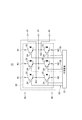
図3は制御基板22の実装状態を模式的に示す図であり、図4は図3のA−A’線における断面を模式的に示す図である。
制御基板22は、図4に示すように、表裏面にGNDパターン51や各種回路が形成された複数層の絶縁層52を積層して成り、図3に示すように、スルーホール55で層間の回路を接続した貫通多層板としての多層基板53で構成されている。この多層基板53には、各種回路として駆動回路など制御回路配線がパターン形成されるとともに、表層には上記GNDパターン51やIC50、電源パターン56、当該電源パターン56とGNDパターン51を接続するバイパスコンデンサ57などが設けられている。バイパスコンデンサ57は、直流電源電圧の変動を抑えて回路の動作安定化を図るために設けられている。FIG. 3 is a diagram schematically showing the mounting state of the
As shown in FIG. 4, the
IC50は、上面視矩形の板状のケーシングにパッケージ化されたチップであり、その両側には多数の接続ピンが設けられている。これらの接続ピンには、電源パターン56に接続される電源ピン60や、GNDパターン51に接続されるGNDピン61が含まれている。GNDピン61は、IC50の両側に複数本ずつ対向して設けられ、放熱フィン63を介してGNDパターン51に接続されている。IC50の両側のGNDピン61は、IC50の内部回路を通じて導通しており、IC50には一方側のGNDピン61か他方側のGNDピン61にかけてIC50を横断するように結ぶGNDライン64が形成されることとなる。
The
制御基板22に設けたGNDパターン51は、IC50の実装時に当該IC50によって覆われる領域に設けられる。本実施形態では、GNDパターン51は、IC50に覆われる領域に設けた主領域51Aと、この主領域51AからIC50のGNDピン61が設けられた両側に向けて延びる接続ピン用領域51Bと、主領域51Aをバイパスコンデンサ57に接続するためのバイパスコンデンサ接続用領域51Cとを含んで形成されている。
The
制御基板22は、上述したように、半導体モジュール20の各パッケージ20Aを覆うように配置されるため、各パッケージ20Aに納めた絶縁基板31と制御基板22とは、図4に示すように、上下に積層配置される。絶縁基板31には、上述のように、パワースイッチング素子24が設けられ、当該パワースイッチング素子24を挟んで直流入力端子40及び交流出力端子41がそれぞれ対向して設けられている。したがって、パワースイッチング素子24のスイッチング動作時には、直流入力端子40から交流出力端子41にかけた向きX(交流/直流変換時は逆向き)に大きな主電流が流れる。
Since the
絶縁基板31に主電流が流れると、当該主電流により磁界が発生するが、絶縁基板31の上に制御基板22が配置されていることから、この制御基板22が磁界に晒されることとなる。このとき、制御基板22に、IC50のGNDライン64、GNDピン61及びGNDパターン51を繋ぐGNDループが形成されていると、このGNDループが磁界に鎖交する場合には、当該GNDループに誘導電流が誘起されるためGND電位が変動し、IC50や制御基板22の各種回路が誤動作する虞が生じる。
そこで、本実施形態では、図3に示すように、制御基板22のGNDパターン51のうちIC50に覆われる上記主領域51Aに、IC50の両側のGNDピン61の間を断絶するように切欠いて成るGNDループ断絶スリット70を設ける構成とし、GNDループが形成されないようにしている。When a main current flows through the insulating
Therefore, in the present embodiment, as shown in FIG. 3, the
図5は、絶縁基板31の主電流に伴う磁界発生と、磁界によって制御基板22に誘起される誘導電流との関係を説明するための等価回路図である。
この図に示すように、絶縁基板31の回路と、制御基板22のGNDパターン51を含む回路との間には相互インダクタンスMが存在している。絶縁基板31の主電流により磁界が発生した場合、制御基板22に、IC50のGNDライン64、GNDピン61及びGNDパターン51から成る磁界に鎖交したGNDループが存在していると、相互インダクタンスMにより当該GNDループに誘導電流が誘起されることとなるが、本実施形態では、上記GNDループ断絶スリット70がGNDループを断絶する断絶部となり当該GNDループが存在しないため、GNDパターン51に誘導電流が誘起されることはない。
これにより、スイッチング時に絶縁基板31に強力な磁界が発生しても、GND電位の変動が抑制されIC50や制御基板22の各種回路の誤動作が防止されることとなる。また、絶縁基板31の主電流の向きXに対するIC50の実装方向(より正確には、GNDライン64の方向)に拘わらず誘導電流の発生を抑制できるため、制御基板22における基板パターンレイアウトの自由度が減ることも無い。FIG. 5 is an equivalent circuit diagram for explaining the relationship between the generation of a magnetic field associated with the main current of the insulating
As shown in this figure, a mutual inductance M exists between the circuit of the insulating
As a result, even if a strong magnetic field is generated in the insulating
上記GNDループ断絶スリット70は、IC50の両側のGNDピン61の間の領域を横断する寸法形状であれば良い。すなわち、GNDループ断絶スリット70は、図3に示すように、その長手方向の一端部である切欠開口端70Aから他端部である底部70Bまでの間に、両側のGNDピン61が全て含まれるような長さ(スリット長)Laに形成されている。この長さLaを、片側の各GNDピン61が配列される範囲である所定の配列長Lbと等しくすることで、GNDループ断絶スリット70によるGNDパターン51の欠損部分を最小にしつつGNDループを断絶することができる。
The GND loop breaking slit 70 may have a dimension and shape that crosses the region between the GND pins 61 on both sides of the
ここで、本実施形態の制御基板22にあっては、GNDパターン51の主領域51Aに設けたGNDループ断絶スリット70の縁部に沿って複数のスルーホール55を配置することとしている。これにより、スイッチング時の磁界によりGNDループ断絶スリット70の両側に電位が誘起された場合でも、当該電位がスルーホール55を通じて他の層のGNDパターン51に導かれるためGND電位安定度の向上を図ることができる。なお、スルーホール55は、GNDループ断絶スリット70を挟んで対向する位置、すなわちGNDループの断絶点に対応した箇所に設けると効果的である。
Here, in the
図6は、GNDパターン51の等価回路を示す図である。
この図に示すように、GNDパターン51は、バイパスコンデンサ57を通じて電源であるVDDに接続され、また、このバイパスコンデンサ57にIC50の両側のGNDピン61がそれぞれ接続されている。また、バイパスコンデンサ57からIC50の両側の各GNDピン61までの間には、バイパスコンデンサ接続用領域51Cの回路インピーダンスZ1と、主領域51Aでの各GNDピン61までの回路インピーダンスZ1、Z2とが含まれる。このとき、主領域51Aには、図3に示すように、GNDループ断絶スリット70の切欠開口端70AがGNDピン61からみてバイパスコンデンサ57とは反対側に設けられているため、バイパスコンデンサ57からみてIC50の両側のGNDピン61がGNDループ断絶スリット70により2手に分岐される形となり、図6に示すように、IC50の両側の各GNDピン61がバイパスコンデンサ57を起点にスター配線形状に接続されることとなる。これにより、主領域51AでのGNDループ断絶スリット70による分岐点Y(図3の底部70Bに相当)からIC50の両側の各GNDピン61までの回路インピーダンスZ2、Z2’が概ね等しくなり、GNDピン61の間の電位差が抑えられる。FIG. 6 is a diagram showing an equivalent circuit of the
As shown in this figure, the
これに対して、図7(A)に示すように、GNDループ断絶スリット70の切欠開口端70Aを、GNDピン61とバイパスコンデンサ57の間に設けた場合には、図7(B)に示すように、バイパスコンデンサ57からみてIC50の両側のGNDピン61がそれぞれ直列に繋がる形となる。この形では、バイパスコンデンサ57からIC50の両側のGNDピン61のそれぞれまでの回路インピーダンスが異なることとなる。したがって、この場合には、GNDパターン51に低インピーダンスの素材を使用するなどして、回路インピーダンスの差異を小さくすることが好ましい。
On the other hand, as shown in FIG. 7 (A), when the
このように、本実施形態によれば、制御基板22にGNDループを断つ断絶部としてのGNDループ断絶スリット70を設ける構成とした。この構成により、パワースイッチング素子24のスイッチングに伴う磁界に制御基板22が晒された場合でも、制御基板22には、磁界に鎖交するGNDループがIC50の実装方向に拘わらず存在することが無い。これにより、GNDパターン51に誘導電流が誘起されることがなくGND電位の変動を抑制し、ICの誤動作を防止できる。
As described above, according to the present embodiment, the
特に、本実施形態によれば、GNDパターン51のIC50で覆われる主領域51Aに、IC50の両側に設けられたGNDピン61の間を横断するように上記断絶部としてのGNDループ断絶スリット70を設ける構成とした。この構成により、制御基板22に実装されるIC50や各種回路のパターンに変更を加える必要がなく、簡単に上記断絶部を構成することができる。
In particular, according to the present embodiment, the GND loop break slit 70 as the break portion is formed in the
また本実施形態によれば、GNDループ断絶スリット70のスリット長Laを、GNDピン61を設けた配列長Lbと等しくする構成としたため、GNDループ断絶スリット70によるGNDパターン51の欠損部分を最小にしつつGNDループを断絶することができる。
In addition, according to the present embodiment, the slit length La of the GND loop break slit 70 is made equal to the arrangement length Lb provided with the GND pins 61, so that the missing portion of the
また本実施形態によれば、制御基板22をスルーホール55で層間の回路を接続する多層基板53で構成し、上記スルーホール55をGNDループ断絶スリット70の縁部に設ける構成とした。この構成により、スイッチング時の磁界によりGNDループ断絶スリット70の両側に電位が誘起された場合でも、当該電位がスルーホール55を通じて他の層に導かれるためGND電位安定度の向上を図ることができる。
In addition, according to the present embodiment, the
また本実施形態によれば、IC50の両側のGNDピン61がバイパスコンデンサ57を起点にスター配線されるようにGNDループ断絶スリット70を設ける構成とした。この構成により、バイパスコンデンサ57からIC50の両側の各GNDピン61までの回路インピーダンスが概ね等しくなるため、GNDピン61の間の電位差が抑えられる。
According to the present embodiment, the GND loop break slit 70 is provided so that the GND pins 61 on both sides of the
なお、本実施形態に対しては、次のような変形が可能である。
例えば、本実施形態では、GNDループ断絶スリット70をGNDパターン51の主領域51Aの範囲内に設ける構成としたが、これに限らず、図8(A)に示すように、GNDループ断絶スリット70をバイパスコンデンサ接続用領域51Cまで延在し、その端部71がバイパスコンデンサ57の近傍に位置するように形成してもよい。この場合においても、GNDループ断絶スリット70がバイパスコンデンサ57からみてIC50の両側のGNDピン61を2手に分岐するように設けられているため、図8(B)に示すように、IC50の両側の各GNDピン61がバイパスコンデンサ57を起点にスター配線形状に接続されることとなる。The following modifications can be made to the present embodiment.
For example, in the present embodiment, the GND loop break slit 70 is provided within the
<第2実施形態>
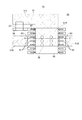
図9は本実施形態に係る制御基板22の実装状態を模式的に示す図であり、図10は図9のA−A’線における断面を示す図である。なお、図9及び図10において、第1実施形態で説明した部材については同一の符号を付し、その説明を省略する。
本実施形態では、次のようにして、IC50のGNDライン64、GNDピン61及びGNDパターン51を繋ぐGNDループが形成されないようにしている。
すなわち、図9に示すように、IC50の一方側に設けたGNDピン61が接続される箇所を避けてGNDパターン51を形成するために、当該GNDパターン51には、IC50の片側にだけ接続ピン用領域51Bを設ける構成としている。この構成により、図10に示すように、IC50とGNDパターン51の間には、IC50の片側にGNDピン61とGNDパターン51の接続を禁止するようにGNDパターン51が欠損したGNDパターン欠損部73が形成される。
このGNDパターン欠損部73により、IC50のGNDライン64、GNDピン61及びGNDパターン51を繋ぐGNDループが断絶されるため、第1実施形態と同様に、スイッチング時に磁界が発生した場合でも、GND電位の変動を抑制でき、IC50や制御基板22の各回路の誤動作を防止することができる。
また、IC50の直下に位置するGNDパターン51の主領域51Aに上記GNDループ断絶スリット70を設ける必要がないため、IC50と主領域51Aとの接触面積が減る事が無く放熱効果を期待できる。Second Embodiment
FIG. 9 is a diagram schematically showing the mounting state of the
In the present embodiment, a GND loop that connects the
That is, as shown in FIG. 9, in order to form the
Since the GND
In addition, since it is not necessary to provide the GND loop break slit 70 in the
<第3実施形態>
図11は本実施形態に係る制御基板22の実装状態を模式的に示す図であり、図12は図11のA−A’線における断面を示す図である。なお、図11及び図12において、第1実施形態で説明した部材については同一の符号を付し、その説明を省略する。
本実施形態では、次のようにして、IC50のGNDライン64、GNDピン61及びGNDパターン51を繋ぐGNDループが形成されないようにしている。
すなわち、本実施形態では、図11に示すように、GNDパターン51にGNDループ断絶スリット70を設けるのではなく、図12に示すように、IC50の内部回路により構成されるGNDライン64に、IC50の両側のGNDピン61同士の導通を断絶する開放部75を設ける構成としている。この開放部75により、IC50のGNDライン64、GNDピン61及びGNDパターン51を繋ぐGNDループが断絶されるため、第1及び第2実施形態と同様に、スイッチング時に磁界が発生した場合でも、GND電位の変動を抑制でき、IC50や制御基板22の各回路の誤動作を防止することができる。<Third Embodiment>
FIG. 11 is a diagram schematically showing a mounting state of the
In the present embodiment, a GND loop that connects the
That is, in the present embodiment, as shown in FIG. 11, the GND pattern break slit 70 is not provided in the
上記開放部75は、IC50の両側のGNDピン61を内部回路で接続せずに、それぞれが電気的に独立するように内部回路を分けることで構成される。この構成によれば、第2実施形態と同様に、IC50の直下に位置するGNDパターン51の主領域51Aに上記GNDループ断絶スリット70を設ける必要がないため、IC50と主領域51Aとの接触面積が減る事が無く放熱効果を期待できる。さらに、制御基板22のGNDパターン51に変更を加える必要がないため、任意のGNDパターン51を有した制御基板22に実装されても、確実に、GNDループが形成されないようにできる。
The
なお、上述した各実施形態は、あくまでも本発明の一態様を示すものであり、本発明の趣旨を逸脱しない範囲で任意に変形及び応用が可能であることは勿論である。 Note that each of the above-described embodiments is merely an aspect of the present invention, and it is needless to say that modifications and applications can be arbitrarily made without departing from the spirit of the present invention.
10 パワーモジュール(半導体装置)
19 ケース体(筐体)
20 半導体モジュール
22 制御基板
24 パワースイッチング素子
30 三相インバータ回路
31 絶縁基板
40 直流入力端子
41 交流出力端子
51 GNDパターン
51A 主領域
51B 接続ピン用領域
51C バイパスコンデンサ接続用領域
53 多層基板
55 スルーホール
57 バイパスコンデンサ
61 GNDピン
64 GNDライン
70 GNDループ断絶スリット(断絶部)
73 GNDパターン欠損部
75 開放部
Z1、Z2、Z2’ 回路インピーダンス10 Power module (semiconductor device)
19 Case body
DESCRIPTION OF
73 GND
Claims (7)
前記ICの両側にはGNDピンが設けられるとともに、前記制御基板には前記ICのGNDピンが接続されるGNDパターンが設けられ、
前記IC、前記ICの両側のGNDピン及び前記GNDパターンが電気的に繋がって形成されるGNDループを断つ断絶部を有することを特徴とする半導体装置。In a semiconductor device in which an insulating substrate provided with a power switching element and a control board provided with an IC for controlling the power switching element are provided vertically in a housing.
A GND pin is provided on both sides of the IC, and a GND pattern to which the GND pin of the IC is connected is provided on the control board,
A semiconductor device comprising: a break portion for breaking a GND loop formed by electrically connecting the IC, GND pins on both sides of the IC, and the GND pattern.
前記ICの両側のGNDピンが前記バイパスコンデンサを起点にスター配線されるように前記GNDループ断絶スリットを設けたことを特徴とする請求項2乃至4のいずれかに記載の半導体装置。The control board is provided with a power supply pattern and a bypass capacitor for connecting the power supply pattern and the GND pattern,
5. The semiconductor device according to claim 2, wherein the GND loop break slit is provided so that the GND pins on both sides of the IC are star-wired starting from the bypass capacitor.
Priority Applications (1)
| Application Number | Priority Date | Filing Date | Title |
|---|---|---|---|
| JP2011552678A JP5524986B2 (en) | 2010-02-03 | 2011-01-20 | Semiconductor device |
Applications Claiming Priority (4)
| Application Number | Priority Date | Filing Date | Title |
|---|---|---|---|
| JP2010022116 | 2010-02-03 | ||
| JP2010022116 | 2010-02-03 | ||
| JP2011552678A JP5524986B2 (en) | 2010-02-03 | 2011-01-20 | Semiconductor device |
| PCT/JP2011/000275 WO2011096164A1 (en) | 2010-02-03 | 2011-01-20 | Semiconductor device |
Publications (2)
| Publication Number | Publication Date |
|---|---|
| JPWO2011096164A1 JPWO2011096164A1 (en) | 2013-06-10 |
| JP5524986B2 true JP5524986B2 (en) | 2014-06-18 |
Family
ID=44355185
Family Applications (1)
| Application Number | Title | Priority Date | Filing Date |
|---|---|---|---|
| JP2011552678A Expired - Fee Related JP5524986B2 (en) | 2010-02-03 | 2011-01-20 | Semiconductor device |
Country Status (4)
| Country | Link |
|---|---|
| US (1) | US8917522B2 (en) |
| JP (1) | JP5524986B2 (en) |
| CN (1) | CN102782843B (en) |
| WO (1) | WO2011096164A1 (en) |
Families Citing this family (5)
| Publication number | Priority date | Publication date | Assignee | Title |
|---|---|---|---|---|
| US9839146B2 (en) * | 2015-10-20 | 2017-12-05 | Cree, Inc. | High voltage power module |
| JP6686663B2 (en) | 2016-04-19 | 2020-04-22 | 株式会社デンソー | Power converter |
| CN105931998B (en) * | 2016-06-17 | 2018-07-20 | 扬州国扬电子有限公司 | A kind of insulating substrate structure and the power module using the substrate |
| JP6549200B2 (en) * | 2017-10-03 | 2019-07-24 | 三菱電機株式会社 | Power conversion circuit |
| JP7081294B2 (en) * | 2018-05-11 | 2022-06-07 | トヨタ自動車株式会社 | Electronic unit |
Citations (5)
| Publication number | Priority date | Publication date | Assignee | Title |
|---|---|---|---|---|
| JPH07169880A (en) * | 1993-03-24 | 1995-07-04 | Intergraph Corp | Multilayer package and packaging method |
| JPH08293578A (en) * | 1995-04-21 | 1996-11-05 | Toshiba Corp | Semiconductor device |
| JP2002184939A (en) * | 2000-12-14 | 2002-06-28 | Mitsubishi Electric Corp | Power module |
| JP2003178895A (en) * | 1997-02-12 | 2003-06-27 | Internatl Rectifier Corp | Integrated circuit for stable control of closed loop/ illumination control |
| JP2005032912A (en) * | 2003-07-10 | 2005-02-03 | Hitachi Industrial Equipment Systems Co Ltd | Power conversion apparatus |
Family Cites Families (2)
| Publication number | Priority date | Publication date | Assignee | Title |
|---|---|---|---|---|
| US6008593A (en) * | 1997-02-12 | 1999-12-28 | International Rectifier Corporation | Closed-loop/dimming ballast controller integrated circuits |
| JP2006165381A (en) * | 2004-12-09 | 2006-06-22 | Toshiba Corp | Semiconductor device |
-
2011
- 2011-01-20 CN CN201180007989.3A patent/CN102782843B/en not_active Expired - Fee Related
- 2011-01-20 JP JP2011552678A patent/JP5524986B2/en not_active Expired - Fee Related
- 2011-01-20 WO PCT/JP2011/000275 patent/WO2011096164A1/en active Application Filing
- 2011-01-20 US US13/576,225 patent/US8917522B2/en active Active
Patent Citations (5)
| Publication number | Priority date | Publication date | Assignee | Title |
|---|---|---|---|---|
| JPH07169880A (en) * | 1993-03-24 | 1995-07-04 | Intergraph Corp | Multilayer package and packaging method |
| JPH08293578A (en) * | 1995-04-21 | 1996-11-05 | Toshiba Corp | Semiconductor device |
| JP2003178895A (en) * | 1997-02-12 | 2003-06-27 | Internatl Rectifier Corp | Integrated circuit for stable control of closed loop/ illumination control |
| JP2002184939A (en) * | 2000-12-14 | 2002-06-28 | Mitsubishi Electric Corp | Power module |
| JP2005032912A (en) * | 2003-07-10 | 2005-02-03 | Hitachi Industrial Equipment Systems Co Ltd | Power conversion apparatus |
Also Published As
| Publication number | Publication date |
|---|---|
| US8917522B2 (en) | 2014-12-23 |
| CN102782843A (en) | 2012-11-14 |
| US20120300418A1 (en) | 2012-11-29 |
| CN102782843B (en) | 2015-05-20 |
| JPWO2011096164A1 (en) | 2013-06-10 |
| WO2011096164A1 (en) | 2011-08-11 |
Similar Documents
| Publication | Publication Date | Title |
|---|---|---|
| US10361609B2 (en) | Electronic device | |
| JP5524986B2 (en) | Semiconductor device | |
| WO2019123818A1 (en) | Power converter | |
| JP2009225612A (en) | Power module | |
| EP2766930B1 (en) | Switching element unit | |
| JP6288769B2 (en) | Semiconductor power module, power conversion device, and moving body using the same | |
| EP2808892B1 (en) | Inverter unit | |
| JP5481104B2 (en) | Semiconductor device | |
| US9748155B2 (en) | Printed circuit board | |
| JP2000133768A (en) | Semiconductor power module | |
| JP6227150B2 (en) | Semiconductor device and multiphase semiconductor device | |
| JP2015207962A (en) | control device | |
| US9866102B2 (en) | Power conversion device | |
| JP2011130626A (en) | Module for semiconductor switch | |
| JP7264855B2 (en) | SUBSTRATE, SEMICONDUCTOR MODULE AND SUBSTRATE MODULE | |
| JP5846929B2 (en) | Power semiconductor module | |
| TWI677172B (en) | Snubber circuit and power semiconductor module and power supply device for induction heating | |
| JP6766965B2 (en) | Power converter | |
| JP6759874B2 (en) | Power converter | |
| JP6676888B2 (en) | Power converter | |
| JP7475925B2 (en) | Electronic substrate | |
| JP2014072344A (en) | Smoothing capacitor | |
| JP6676212B2 (en) | Electronic module and power supply | |
| JP6674398B2 (en) | Wiring structure of power converter and control line | |
| JP2021163817A (en) | Electronic substrate |
Legal Events
| Date | Code | Title | Description |
|---|---|---|---|
| A621 | Written request for application examination |
Free format text: JAPANESE INTERMEDIATE CODE: A621 Effective date: 20130611 |
|
| TRDD | Decision of grant or rejection written | ||
| A01 | Written decision to grant a patent or to grant a registration (utility model) |
Free format text: JAPANESE INTERMEDIATE CODE: A01 Effective date: 20140408 |
|
| A61 | First payment of annual fees (during grant procedure) |
Free format text: JAPANESE INTERMEDIATE CODE: A61 Effective date: 20140410 |
|
| R150 | Certificate of patent or registration of utility model |
Ref document number: 5524986 Country of ref document: JP Free format text: JAPANESE INTERMEDIATE CODE: R150 |
|
| LAPS | Cancellation because of no payment of annual fees |