JP5514407B2 - Display device and driving method thereof - Google Patents
Display device and driving method thereof Download PDFInfo
- Publication number
- JP5514407B2 JP5514407B2 JP2008149201A JP2008149201A JP5514407B2 JP 5514407 B2 JP5514407 B2 JP 5514407B2 JP 2008149201 A JP2008149201 A JP 2008149201A JP 2008149201 A JP2008149201 A JP 2008149201A JP 5514407 B2 JP5514407 B2 JP 5514407B2
- Authority
- JP
- Japan
- Prior art keywords
- signal
- gate
- gate clock
- output enable
- high level
- Prior art date
- Legal status (The legal status is an assumption and is not a legal conclusion. Google has not performed a legal analysis and makes no representation as to the accuracy of the status listed.)
- Active
Links
- 238000000034 method Methods 0.000 title claims description 11
- 239000003990 capacitor Substances 0.000 claims description 41
- 230000004044 response Effects 0.000 claims description 20
- 239000004973 liquid crystal related substance Substances 0.000 claims description 14
- 239000010409 thin film Substances 0.000 claims description 12
- 230000000630 rising effect Effects 0.000 claims description 7
- 238000006243 chemical reaction Methods 0.000 description 14
- 238000010586 diagram Methods 0.000 description 11
- 239000000758 substrate Substances 0.000 description 9
- 229910021417 amorphous silicon Inorganic materials 0.000 description 4
- 230000004048 modification Effects 0.000 description 4
- 238000012986 modification Methods 0.000 description 4
- 238000004519 manufacturing process Methods 0.000 description 3
- 238000002834 transmittance Methods 0.000 description 3
- 230000003111 delayed effect Effects 0.000 description 2
- 230000005684 electric field Effects 0.000 description 2
- 239000011159 matrix material Substances 0.000 description 2
- 230000008859 change Effects 0.000 description 1
- 230000003760 hair shine Effects 0.000 description 1
- 230000008569 process Effects 0.000 description 1
- 230000008054 signal transmission Effects 0.000 description 1
Images


Classifications
-
- G—PHYSICS
- G09—EDUCATION; CRYPTOGRAPHY; DISPLAY; ADVERTISING; SEALS
- G09G—ARRANGEMENTS OR CIRCUITS FOR CONTROL OF INDICATING DEVICES USING STATIC MEANS TO PRESENT VARIABLE INFORMATION
- G09G3/00—Control arrangements or circuits, of interest only in connection with visual indicators other than cathode-ray tubes
- G09G3/20—Control arrangements or circuits, of interest only in connection with visual indicators other than cathode-ray tubes for presentation of an assembly of a number of characters, e.g. a page, by composing the assembly by combination of individual elements arranged in a matrix no fixed position being assigned to or needed to be assigned to the individual characters or partial characters
- G09G3/34—Control arrangements or circuits, of interest only in connection with visual indicators other than cathode-ray tubes for presentation of an assembly of a number of characters, e.g. a page, by composing the assembly by combination of individual elements arranged in a matrix no fixed position being assigned to or needed to be assigned to the individual characters or partial characters by control of light from an independent source
- G09G3/36—Control arrangements or circuits, of interest only in connection with visual indicators other than cathode-ray tubes for presentation of an assembly of a number of characters, e.g. a page, by composing the assembly by combination of individual elements arranged in a matrix no fixed position being assigned to or needed to be assigned to the individual characters or partial characters by control of light from an independent source using liquid crystals
- G09G3/3611—Control of matrices with row and column drivers
- G09G3/3648—Control of matrices with row and column drivers using an active matrix
-
- G—PHYSICS
- G09—EDUCATION; CRYPTOGRAPHY; DISPLAY; ADVERTISING; SEALS
- G09G—ARRANGEMENTS OR CIRCUITS FOR CONTROL OF INDICATING DEVICES USING STATIC MEANS TO PRESENT VARIABLE INFORMATION
- G09G3/00—Control arrangements or circuits, of interest only in connection with visual indicators other than cathode-ray tubes
- G09G3/20—Control arrangements or circuits, of interest only in connection with visual indicators other than cathode-ray tubes for presentation of an assembly of a number of characters, e.g. a page, by composing the assembly by combination of individual elements arranged in a matrix no fixed position being assigned to or needed to be assigned to the individual characters or partial characters
-
- G—PHYSICS
- G02—OPTICS
- G02F—OPTICAL DEVICES OR ARRANGEMENTS FOR THE CONTROL OF LIGHT BY MODIFICATION OF THE OPTICAL PROPERTIES OF THE MEDIA OF THE ELEMENTS INVOLVED THEREIN; NON-LINEAR OPTICS; FREQUENCY-CHANGING OF LIGHT; OPTICAL LOGIC ELEMENTS; OPTICAL ANALOGUE/DIGITAL CONVERTERS
- G02F1/00—Devices or arrangements for the control of the intensity, colour, phase, polarisation or direction of light arriving from an independent light source, e.g. switching, gating or modulating; Non-linear optics
- G02F1/01—Devices or arrangements for the control of the intensity, colour, phase, polarisation or direction of light arriving from an independent light source, e.g. switching, gating or modulating; Non-linear optics for the control of the intensity, phase, polarisation or colour
- G02F1/13—Devices or arrangements for the control of the intensity, colour, phase, polarisation or direction of light arriving from an independent light source, e.g. switching, gating or modulating; Non-linear optics for the control of the intensity, phase, polarisation or colour based on liquid crystals, e.g. single liquid crystal display cells
- G02F1/133—Constructional arrangements; Operation of liquid crystal cells; Circuit arrangements
- G02F1/1333—Constructional arrangements; Manufacturing methods
- G02F1/1345—Conductors connecting electrodes to cell terminals
-
- G—PHYSICS
- G09—EDUCATION; CRYPTOGRAPHY; DISPLAY; ADVERTISING; SEALS
- G09G—ARRANGEMENTS OR CIRCUITS FOR CONTROL OF INDICATING DEVICES USING STATIC MEANS TO PRESENT VARIABLE INFORMATION
- G09G3/00—Control arrangements or circuits, of interest only in connection with visual indicators other than cathode-ray tubes
- G09G3/20—Control arrangements or circuits, of interest only in connection with visual indicators other than cathode-ray tubes for presentation of an assembly of a number of characters, e.g. a page, by composing the assembly by combination of individual elements arranged in a matrix no fixed position being assigned to or needed to be assigned to the individual characters or partial characters
- G09G3/34—Control arrangements or circuits, of interest only in connection with visual indicators other than cathode-ray tubes for presentation of an assembly of a number of characters, e.g. a page, by composing the assembly by combination of individual elements arranged in a matrix no fixed position being assigned to or needed to be assigned to the individual characters or partial characters by control of light from an independent source
- G09G3/36—Control arrangements or circuits, of interest only in connection with visual indicators other than cathode-ray tubes for presentation of an assembly of a number of characters, e.g. a page, by composing the assembly by combination of individual elements arranged in a matrix no fixed position being assigned to or needed to be assigned to the individual characters or partial characters by control of light from an independent source using liquid crystals
- G09G3/3611—Control of matrices with row and column drivers
- G09G3/3674—Details of drivers for scan electrodes
- G09G3/3677—Details of drivers for scan electrodes suitable for active matrices only
-
- G—PHYSICS
- G11—INFORMATION STORAGE
- G11C—STATIC STORES
- G11C19/00—Digital stores in which the information is moved stepwise, e.g. shift registers
- G11C19/18—Digital stores in which the information is moved stepwise, e.g. shift registers using capacitors as main elements of the stages
- G11C19/182—Digital stores in which the information is moved stepwise, e.g. shift registers using capacitors as main elements of the stages in combination with semiconductor elements, e.g. bipolar transistors, diodes
- G11C19/184—Digital stores in which the information is moved stepwise, e.g. shift registers using capacitors as main elements of the stages in combination with semiconductor elements, e.g. bipolar transistors, diodes with field-effect transistors, e.g. MOS-FET
-
- G—PHYSICS
- G09—EDUCATION; CRYPTOGRAPHY; DISPLAY; ADVERTISING; SEALS
- G09G—ARRANGEMENTS OR CIRCUITS FOR CONTROL OF INDICATING DEVICES USING STATIC MEANS TO PRESENT VARIABLE INFORMATION
- G09G2300/00—Aspects of the constitution of display devices
- G09G2300/04—Structural and physical details of display devices
- G09G2300/0404—Matrix technologies
- G09G2300/0417—Special arrangements specific to the use of low carrier mobility technology
-
- G—PHYSICS
- G09—EDUCATION; CRYPTOGRAPHY; DISPLAY; ADVERTISING; SEALS
- G09G—ARRANGEMENTS OR CIRCUITS FOR CONTROL OF INDICATING DEVICES USING STATIC MEANS TO PRESENT VARIABLE INFORMATION
- G09G2310/00—Command of the display device
- G09G2310/08—Details of timing specific for flat panels, other than clock recovery
-
- G—PHYSICS
- G09—EDUCATION; CRYPTOGRAPHY; DISPLAY; ADVERTISING; SEALS
- G09G—ARRANGEMENTS OR CIRCUITS FOR CONTROL OF INDICATING DEVICES USING STATIC MEANS TO PRESENT VARIABLE INFORMATION
- G09G2320/00—Control of display operating conditions
- G09G2320/04—Maintaining the quality of display appearance
- G09G2320/041—Temperature compensation
Description
本発明は表示装置に関し、特にその駆動方法に関する。 The present invention relates to a display device, and more particularly to a driving method thereof.
表示装置は一般に、表示パネル、ゲート駆動部、及びデータ駆動部を備えている。表示パネルには複数の画素が備えられ、それらの間を複数のゲート線と複数のデータ線とが延びている。各画素には一般に、ゲート線とデータ線とが一本ずつ接続されている。ゲート駆動部は複数のゲート線に対してゲートオン信号を順番に印加する。データ駆動部は複数のデータ線に対してデータ信号を印加する。各画素はゲートオン信号に応じてデータ信号を受信し、更にそのデータ信号に応じた階調の輝度で光る。こうして、表示パネルには所望の画像が表示される。 A display device generally includes a display panel, a gate driver, and a data driver. The display panel includes a plurality of pixels, and a plurality of gate lines and a plurality of data lines extend between them. In general, one gate line and one data line are connected to each pixel. The gate driver sequentially applies gate-on signals to the plurality of gate lines. The data driver applies data signals to the plurality of data lines. Each pixel receives a data signal in accordance with the gate-on signal, and further shines with a luminance of gradation corresponding to the data signal. Thus, a desired image is displayed on the display panel.
従来の表示装置ではゲート駆動部がICチップに組み込まれている。このICチップは一般には表示パネルの表示領域の周辺に実装され、各ゲート線に接続されている。この実装方式では一般に、ゲート駆動部とゲート線との間の接続不良を更に低減させることが困難である。また、ゲート駆動部の製作コストを更に削減することが困難である。 In a conventional display device, a gate driving unit is incorporated in an IC chip. This IC chip is generally mounted around the display area of the display panel and connected to each gate line. In this mounting method, it is generally difficult to further reduce the connection failure between the gate driver and the gate line. In addition, it is difficult to further reduce the manufacturing cost of the gate driver.
上記の困難を克服するために、近年では、ゲート駆動部を表示パネルの上に直接集積化し、一体的に製作している。好ましくは、表示パネルの一辺に沿ってゲート駆動部が集積化されている。この場合、ゲート駆動部とゲート線との間の接続不良を更に低減させることが容易であり、ゲート駆動部の製作コストを更に削減できる。
表示パネルには一般にアモルファスシリコンが利用されているので、ゲート駆動部を表示パネルと一体的に製作する場合、ゲート駆動部を構成する回路素子は一般にアモルファスシリコンから製作される。一般に、アモルファスシリコンは温度によって電子の移動度が大幅に変わる。従って、アモルファスシリコンから製作された回路素子は、周りの温度が低すぎる場合、その応答速度が十分には上がらない。特にゲート駆動部は、周りの温度が低すぎる場合、ゲートオン信号の電圧レベルが不十分になりやすい。さらに、ゲート駆動部が各段のゲート線に対するゲートオン信号の印加タイミングを、前段のゲート線から印加されたゲートオン信号に基づいて決定する場合、前段のゲート線でゲートオン信号の電圧レベルが低すぎれば、後段のゲート線でもゲートオン信号の電圧レベルが十分には上がらない。このように、ゲート駆動部を表示パネルと一体的に製作する場合には、周辺温度の過度の低下に伴って表示パネルが画像を正常には表示できなくなる危険性がある。 Since amorphous silicon is generally used for the display panel, when the gate driving unit is manufactured integrally with the display panel, circuit elements constituting the gate driving unit are generally manufactured from amorphous silicon. In general, the mobility of electrons in amorphous silicon varies greatly with temperature. Therefore, the response speed of the circuit element manufactured from amorphous silicon is not sufficiently increased when the ambient temperature is too low. In particular, when the ambient temperature is too low, the gate driving unit tends to have an insufficient voltage level of the gate-on signal. Furthermore, when the gate driver determines the application timing of the gate-on signal to the gate line of each stage based on the gate-on signal applied from the previous-stage gate line, the voltage level of the gate-on signal is too low on the previous-stage gate line. Even in the subsequent gate line, the voltage level of the gate-on signal does not rise sufficiently. Thus, when the gate driving unit is manufactured integrally with the display panel, there is a risk that the display panel cannot normally display an image as the ambient temperature is excessively lowered.
本発明の目的は、表示パネルと一体化されたゲート駆動部に低温下でもゲートオン信号の電圧レベルを十分に高く上昇させることにより、低温下であっても画像表示をスムーズに行うことのできる表示装置を提供することにある。 An object of the present invention is to provide a display that can smoothly display an image even at a low temperature by raising the voltage level of a gate-on signal sufficiently high even at a low temperature in a gate driver integrated with a display panel. To provide an apparatus.
本発明の一つの観点による表示装置は、表示パネル、ゲートクロック生成部、及びゲート駆動部を備えている。表示パネルは複数の画素と、それらに接続された複数のゲート線とを有する。ゲートクロック生成部は、ゲートクロック信号と、その反転信号であるゲートクロックバー信号とを生成し、第1の垂直開始信号を入力し、第1の垂直同期開始信号のレベルを変換して、第2の垂直同期開始信号を出力する。ゲートクロック生成部は特に、各フレームでゲートクロック信号が最初にハイレベルに維持される期間(以下、ハイレベル期間と略す。)を後続のハイレベル期間より狭める。好ましくは、各フレームでゲートクロック信号の最初のハイレベル期間は1水平周期の30〜60%であり、後続のハイレベル期間は1水平周期である。ゲートクロック生成部は更に、各フレームの開始時点からゲートクロック信号の最初のハイレベル期間の開始時点まではゲートクロックバー信号をローレベルに維持する。ゲート駆動部は、ゲートクロック信号及びゲートクロックバー信号に応じて複数のゲート線に対してゲートオン信号を順番に印加する。ゲート駆動部は、表示パネルに集積化されて複数のゲート線のそれぞれに一つずつ接続された複数のステージ部を備える。複数のステージ部は、第1のキャパシタと第1のトランジスタを備える。第1のキャパシタの正極が第1のトランジスタのゲート端子に接続され、第1のキャパシタの負極が、各ステージ部の出力端子に接続される。第1のトランジスタのソース端子は、ゲートクロック信号が印加され、第1のトランジスタのドレイン端子は、各ステージ部の出力端子に接続される。第1のキャパシタは、各フレームの開始時点からゲートクロック信号の最初のハイレベル期間の開始時点まで第2の垂直同期開始信号によって充電され、ゲートクロック信号の最初のハイレベル期間の開始時点から終了時点までゲートクロック信号によって充電される。 A display device according to one aspect of the present invention includes a display panel, a gate clock generation unit, and a gate driving unit. The display panel includes a plurality of pixels and a plurality of gate lines connected to the pixels. The gate clock generation unit generates a gate clock signal and a gate clock bar signal that is an inverted signal thereof , inputs the first vertical start signal, converts the level of the first vertical synchronization start signal, 2 vertical synchronization start signals are output . In particular, the gate clock generator narrows a period during which the gate clock signal is initially maintained at a high level in each frame (hereinafter abbreviated as a high level period) from a subsequent high level period. Preferably, in each frame, the first high level period of the gate clock signal is 30 to 60% of one horizontal period, and the subsequent high level period is one horizontal period. The gate clock generator further maintains the gate clock bar signal at a low level from the start time of each frame to the start time of the first high level period of the gate clock signal. The gate driver sequentially applies gate-on signals to the plurality of gate lines according to the gate clock signal and the gate clock bar signal. The gate driving unit includes a plurality of stage units integrated on the display panel and connected to each of the plurality of gate lines. The plurality of stage units include a first capacitor and a first transistor. The positive electrode of the first capacitor is connected to the gate terminal of the first transistor, and the negative electrode of the first capacitor is connected to the output terminal of each stage unit. A gate clock signal is applied to the source terminal of the first transistor, and the drain terminal of the first transistor is connected to the output terminal of each stage unit. The first capacitor is charged by the second vertical synchronization start signal from the start of each frame to the start of the first high level period of the gate clock signal, and ends from the start of the first high level period of the gate clock signal. It is charged by the gate clock signal until the time.
本発明によるこの表示装置は好ましくは信号制御部と信号変換部とを更に備えている。信号制御部は、第1の出力イネーブル信号、第1の垂直同期開始信号、及び駆動クロック信号を生成する。信号変換部は第1の出力イネーブル信号と第1の垂直同期開始信号とに応じ、各フレームでの最初のハイレベル期間を除いて第1の出力イネーブル信号と等価な第2の出力イネーブル信号を出力する。第2の出力イネーブル信号は好ましくは、第1の垂直同期開始信号のハイレベル期間に第1の出力イネーブル信号をローレベルに維持した信号である。 This display device according to the present invention preferably further comprises a signal controller and a signal converter. The signal control unit generates a first output enable signal, a first vertical synchronization start signal, and a drive clock signal. In response to the first output enable signal and the first vertical synchronization start signal, the signal converter outputs a second output enable signal equivalent to the first output enable signal except for the first high level period in each frame. Output. The second output enable signal is preferably a signal obtained by maintaining the first output enable signal at the low level during the high level period of the first vertical synchronization start signal.
信号変換部は好ましくは、二つの端子とスイッチ部とを備えている。第1の端子に対しては第1の出力イネーブル信号が入力される。第2の端子は第1の端子に接続され、外部に第2の出力イネーブル信号を出力する。スイッチ部は、第1の端子と第2の端子との間の接続点を、第1の垂直同期開始信号がハイレベルのときに接地する。信号変換部はその他に、二つの論理ゲートを備えていても良い。第1の論理ゲートは、第1の垂直同期開始信号と第1の出力イネーブル信号との論理積の否定を求める。第2の論理ゲートは、第1の論理ゲートの出力と第1の出力イネーブル信号との論理積を求める。第2の論理ゲートの出力が第2の出力イネーブル信号として、ゲートクロック生成部によって利用される。 The signal conversion unit preferably includes two terminals and a switch unit. The first output enable signal is input to the first terminal. The second terminal is connected to the first terminal and outputs a second output enable signal to the outside. The switch unit grounds a connection point between the first terminal and the second terminal when the first vertical synchronization start signal is at a high level . In addition, the signal conversion unit may include two logic gates. The first logic gate obtains the negation of the logical product of the first vertical synchronization start signal and the first output enable signal. The second logic gate obtains a logical product of the output of the first logic gate and the first output enable signal. The output of the second logic gate is used as a second output enable signal by the gate clock generator.
ゲートクロック生成部は好ましくは、第2の出力イネーブル信号と駆動クロック信号とに基づいてゲートクロック信号及びゲートクロックバー信号を生成する。ゲートクロック生成部は更に好ましくは、第1の垂直同期開始信号がハイレベルの場合において、第2の出力イネーブル信号と駆動クロック信号との論理和が0であれば、ゲートクロック信号とゲートクロックバー信号とをいずれもローレベルに維持し、第2の出力イネーブル信号と駆動クロック信号との論理和が1であれば、ゲートクロック信号をハイレベルに維持し、ゲートクロックバー信号をローレベルに維持し、第1の垂直同期開始信号がローレベルの場合において、第2の出力イネーブル信号と駆動クロック信号との論理和が0である場合、ゲートクロック信号及びゲートクロックバー信号の各論理レベルを反転させる。 The gate clock generator preferably generates a gate clock signal and a gate clock bar signal based on the second output enable signal and the drive clock signal. More preferably, when the first vertical synchronization start signal is at a high level and the logical sum of the second output enable signal and the drive clock signal is 0, the gate clock generation unit preferably has a gate clock signal and a gate clock bar. If the logical sum of the second output enable signal and the drive clock signal is 1, the gate clock signal is maintained at the high level and the gate clock bar signal is maintained at the low level. If the logical sum of the second output enable signal and the drive clock signal is 0 when the first vertical synchronization start signal is low level, the logic levels of the gate clock signal and the gate clock bar signal are inverted. Let
ゲートクロック生成部は好ましくは、第1の垂直同期開始信号のレベルを変換して第2の垂直同期開始信号として出力する。ゲート駆動部は好ましくは、各フレームで第2の垂直同期開始信号に応じてゲートオン信号の印加動作を開始する。ゲート駆動部は好ましくは複数のステージ部を備えている。各ステージ部は表示パネルに集積化され、ゲート線に一つずつ接続されている。特に、第1のゲート線に接続された第1のステージ部は、第2の垂直同期開始信号と、各フレームでのゲートクロック信号の最初の立ち上がりとに応じてゲートオン信号を第1のゲート線に出力する。一方、他のステージ部はそれぞれ、前段のステージ部から前段のゲート線に出力される信号と、ゲートクロック信号、及びゲートクロックバー信号に応じてゲート線の一つにゲートオン信号を出力する。 The gate clock generator preferably converts the level of the first vertical synchronization start signal and outputs it as the second vertical synchronization start signal. The gate driver preferably starts the gate-on signal application operation in response to the second vertical synchronization start signal in each frame. The gate driving unit preferably includes a plurality of stage units. Each stage unit is integrated on the display panel and connected to the gate line one by one. In particular, the first stage connected to the first gate line sends a gate-on signal to the first gate line in response to the second vertical synchronization start signal and the first rising edge of the gate clock signal in each frame. Output to. On the other hand, each of the other stage units outputs a gate-on signal to one of the gate lines in response to the signal output from the previous stage unit to the previous gate line, the gate clock signal, and the gate clock bar signal.
本発明の他の観点による表示装置は、表示パネル、信号制御部、ゲートクロック生成部、及びゲート駆動部を備えている。表示パネルは複数の画素と、それらに接続された複数のゲート線とを有する。ゲートクロック生成部はゲートクロック信号と、その反転信号であるゲートクロックバー信号とを生成し、第1の垂直開始信号を入力し、第1の垂直同期開始信号のレベルを変換して、第2の垂直同期開始信号を出力する。ゲートクロック生成部は特に、第1の垂直同期開始信号のハイレベル期間では第1の出力イネーブル信号をローレベルに変化させて第2の出力イネーブル信号として出力する。ゲートクロック生成部は更に、第2の出力イネーブル信号と駆動クロック信号とに基づき、各フレームでゲートクロック信号の最初のハイレベル期間を後続のハイレベル期間より狭める。ゲートクロック生成部はその上、各フレームの開始時点からゲートクロック信号の最初のハイレベル期間の開始時点まではゲートクロックバー信号をローレベルに維持する。ゲート駆動部は、第2の垂直同期開始信号、ゲートクロック信号、及びゲートクロックバー信号に応じて複数のゲート線に対してゲートオン信号を順番に印加する。ゲート駆動部は、表示パネルに集積化されて複数のゲート線のそれぞれに一つずつ接続された複数のステージ部を備える。第1のキャパシタの正極が第1のトランジスタのゲート端子に接続され、第1のキャパシタの負極が、各ステージ部の出力端子に接続される。第1のトランジスタのソース端子は、ゲートクロック信号が印加され、第1のトランジスタのドレイン端子は、各ステージ部の出力端子に接続される。第1のキャパシタは、各フレームの開始時点からゲートクロック信号の最初のハイレベル期間の開始時点まで第2の垂直同期開始信号によって充電され、ゲートクロック信号の最初のハイレベル期間の開始時点から終了時点までゲートクロック信号によって充電される。 A display device according to another aspect of the present invention includes a display panel, a signal control unit, a gate clock generation unit, and a gate drive unit. The display panel includes a plurality of pixels and a plurality of gate lines connected to the pixels. Gate clock generator and No. Getokuro' click signal, and generates a gate clock bar signal which is the inverted signal, the first vertical start signal inputted, converts the level of the first vertical sync start signal, the 2 vertical synchronization start signals are output . In particular, the gate clock generation unit changes the first output enable signal to the low level and outputs it as the second output enable signal during the high level period of the first vertical synchronization start signal. The gate clock generator further narrows the first high level period of the gate clock signal in each frame from the subsequent high level period based on the second output enable signal and the drive clock signal. In addition, the gate clock generator maintains the gate clock bar signal at a low level from the start time of each frame to the start time of the first high level period of the gate clock signal. The gate driver sequentially applies gate-on signals to the plurality of gate lines according to the second vertical synchronization start signal, the gate clock signal, and the gate clock bar signal. The gate driving unit includes a plurality of stage units integrated on the display panel and connected to each of the plurality of gate lines. The positive electrode of the first capacitor is connected to the gate terminal of the first transistor, and the negative electrode of the first capacitor is connected to the output terminal of each stage unit. A gate clock signal is applied to the source terminal of the first transistor, and the drain terminal of the first transistor is connected to the output terminal of each stage unit. The first capacitor is charged by the second vertical synchronization start signal from the start of each frame to the start of the first high level period of the gate clock signal, and ends from the start of the first high level period of the gate clock signal. It is charged by the gate clock signal until the time.
本発明による表示装置は、垂直同期開始信号に応じ、各フレームで出力イネーブル信号から最初のハイレベル期間を除去し、ローレベルに維持する。それにより、各フレームでゲートクロック信号の最初のハイレベル期間が後続のハイレベル期間より狭められる。特に、ゲートクロック信号の最初の立ち上がりが垂直同期開始信号の立ち上がりから遅れる。ゲート駆動部はその遅れの間に起動すれば良い。従って、ゲート駆動部が表示パネルに集積化されている場合でも、ゲート駆動部は周辺の温度の低下に伴う応答速度の低下に関わらず、ゲートクロック信号の最初のハイレベル期間に出力されるゲートオン信号を十分に高いレベルまで上昇させることができる。こうして、本発明による表示装置は低温下でも画像表示をスムーズに行うことができる。 In accordance with the vertical synchronization start signal, the display device according to the present invention removes the first high level period from the output enable signal in each frame and maintains the low level. Thus, the first high level period of the gate clock signal is narrowed in each frame from the subsequent high level period. In particular, the first rising edge of the gate clock signal is delayed from the rising edge of the vertical synchronization start signal. The gate driver may be activated during the delay. Therefore, even when the gate driver is integrated in the display panel, the gate driver does not turn on the gate on which is output during the first high level period of the gate clock signal, regardless of the decrease in the response speed due to the decrease in the ambient temperature. The signal can be raised to a sufficiently high level. Thus, the display device according to the present invention can smoothly display an image even at a low temperature.
本発明による表示装置では特に、ゲートクロック生成部の前段に設置されたスイッチまたは論理回路を用い、出力イネーブル信号の論理状態を変化させる。それにより、表示装置の製作コストを低く抑えたまま、表示装置に上記の機能を与えることができる。 In the display device according to the present invention, in particular, the logic state of the output enable signal is changed by using a switch or a logic circuit installed in the previous stage of the gate clock generator. Thereby, the above function can be given to the display device while keeping the manufacturing cost of the display device low.
以下、添付の図面を参照しながら、本発明の好適な実施形態について詳細に説明する。
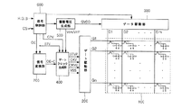
図1は本発明の実施形態による表示装置のブロック図である。図1に示されているように、その表示装置は好ましくは、表示パネル100、ゲート駆動部200、データ駆動部300、ゲートクロック生成部400、駆動電圧生成部500、信号制御部600、及び信号変換部700を備えている。
Hereinafter, preferred embodiments of the present invention will be described in detail with reference to the accompanying drawings.
FIG. 1 is a block diagram of a display device according to an embodiment of the present invention. As shown in FIG. 1, the display device preferably has a
表示パネル100は、一方向に延びている複数のゲート線G1〜Gn、及びゲート線と直交する方向に延びている複数のデータ線D1〜Dmを備えている。表示パネル100は更に、ゲート線G1〜Gnとデータ線D1〜Dmとの間に複数の画素を備えている。複数の画素は好ましくはマトリクス状に配置され、表示パネルの表示領域を構成している。画素はそれぞれ、薄膜トランジスタT1及び液晶キャパシタClcを備えている。各薄膜トランジスタT1には好ましくは、ゲート線G1〜Gnとデータ線D1〜Dmとが一本ずつ接続されている。各画素は維持キャパシタCstをさらに備えていてもよい。
The
図には示されていないが、表示パネル100は好ましくは、透明な上部基板と下部基板とを備えている。下部基板には好ましくは、薄膜トランジスタT、ゲート線G1〜Gn、データ線D1〜Dm、画素電極、及び維持電極が設けられている。ここで、画素電極は液晶キャパシタClc及び維持キャパシタCstの一方の電極であり、維持電極は維持キャパシタCstの他方の電極である。上部基板には好ましくは、遮光パターン、カラーフィルタ、及び共通電極が設けられている。ここで、遮光パターンは好ましくはブラックマトリックスであり、画素間からの光漏れを防ぐ。カラーフィルタは好ましくは赤色、緑色、または青色のいずれかであり、各画素を覆ってその透過光の色を決める。共通電極は、下部基板に面した上部基板の表面全体を覆い、液晶キャパシタClcの他方の電極として機能する。下部基板と上部基板との間には液晶層が挟まれている。液晶層は液晶キャパシタClcの誘電体として機能する。
Although not shown in the figure, the
各画素では、薄膜トランジスタTのゲート端子はゲート線G1〜Gnのいずれかに接続され、ソース端子はデータ線D1〜Dmのいずれかに接続され、ドレイン端子は画素電極に接続されている。薄膜トランジスタTは、ゲート線から制御端子に対して印加されるゲートオン信号に応じてオンオフ動作を行う。オンした薄膜トランジスタT1はデータ線D1〜Dmを画素電極に接続する。それにより、データ信号がそのデータ線から画素電極に供給される。そのとき、液晶キャパシタClcでは両端電圧が変化するので、液晶層内の電界が変化する。その変化に応じて液晶の配列が変化するので液晶層の光透過率が変化する。従って、データ信号の電圧レベルを調節すれば、各画素の光透過率を調節できる。 In each pixel, the gate terminal of the thin film transistor T is connected to one of the gate lines G1 to Gn, the source terminal is connected to one of the data lines D1 to Dm, and the drain terminal is connected to the pixel electrode. The thin film transistor T performs an on / off operation in response to a gate on signal applied from the gate line to the control terminal. The turned-on thin film transistor T1 connects the data lines D1 to Dm to the pixel electrode. Thereby, a data signal is supplied from the data line to the pixel electrode. At that time, since the voltage across the liquid crystal capacitor Clc changes, the electric field in the liquid crystal layer changes. Since the alignment of the liquid crystal changes according to the change, the light transmittance of the liquid crystal layer changes. Therefore, the light transmittance of each pixel can be adjusted by adjusting the voltage level of the data signal.
画素電極には好ましくは多数の切り込みや突起のパターンが設けられている。それにより、液晶層内に生じる電界の方向や強度が調整されるので、液晶の配列方向が調整される。同様に、共通電極に突起や切り込みのパターンが設けられていてもよい。この実施形態では好ましくは、液晶表示方式として垂直配向方式が採用されている。 The pixel electrode is preferably provided with a large number of notches and protrusion patterns. Thereby, the direction and intensity of the electric field generated in the liquid crystal layer are adjusted, so that the alignment direction of the liquid crystal is adjusted. Similarly, the common electrode may be provided with a projection or notch pattern. In this embodiment, the vertical alignment method is preferably employed as the liquid crystal display method.
表示パネル100の外側には、データ駆動部300、ゲートクロック生成部400、駆動電圧生成部500、信号制御部600、及び信号変換部700が設けられている。それらの制御回路は好ましくは一旦ICチップに組み込まれ、その上で表示パネル100に実装されている。各制御回路のチップは別々であっても、それらのいくつかが単一のチップに集積化されていてもよい。更に、それらの一部が表示パネル100と一体的に製作されていてもよい。各チップは表示パネル100の上に直接実装されていても、TCP方式で実装されていても、表示パネル100とは別のプリント回路基板に実装されていても良い。
Outside the
表示パネル100の外側にはゲート駆動部200も設けられている。この実施形態においては、ゲート駆動部200は表示パネル100の下部基板に集積化されている。すなわち、ゲート駆動部200の各回路素子は各画素の薄膜トランジスタTと共に、表示パネル100に一体的に製作されている。
A
信号制御部600は、外部のグラフィックスコントローラ(図示せず)から画像信号R、G、Bと画像制御信号CSとを受信する。画像信号R、G、Bは各画素に対する輝度データ、好ましくは、赤色、緑色、及び青色の各階調値を含む。画像制御信号CSは好ましくは、垂直同期信号、水平同期信号、メインクロック、及びデータイネーブル信号を含む。信号制御部600は、画像信号R、G、Bを表示パネル100の動作条件に合わせて処理する。信号制御部600は更に、画像制御信号CSに基づき、ゲート制御信号及びデータ制御信号を生成する。信号制御部600は、ゲート制御信号を信号変換部700とゲートクロック生成部400とに送り、画像信号R、G、Bとデータ制御信号とをデータ駆動部300に送る。信号制御部600はその他に、所定の電源電圧及び制御信号を駆動電圧生成部500に供給する。
The
ゲート制御信号は好ましくは、第1の出力イネーブル信号OE、第1の垂直同期開始信号STV、及び駆動クロック信号CPVを含む。第1の出力イネーブル信号OEは好ましくは正論理の信号であり、周期が1水平周期(以下、1Hと略す。)に等しい。第1の出力イネーブル信号OEは好ましくは、各1Hの開始時点から少し遅れて立ち上がり、1Hの半分が経過した時点で立ち下がる。第1の垂直同期開始信号STVは、各フレームの開始時期を示す信号であり、好ましくは正論理の信号であり、各フレームの開始時点から所定時間、ハイレベルに維持される。駆動クロック信号CPVは好ましくは正論理の信号であり、周期が1Hに等しい。駆動クロック信号CPVは好ましくは、各1Hの開始時点で立ち下がり、1Hの半分が経過した時点で立ち上がる。好ましくは、駆動クロック信号CPVの立ち上がり期間は第1の出力イネーブル信号OEの立ち下がり期間と重なっている。 The gate control signal preferably includes a first output enable signal OE, a first vertical synchronization start signal STV, and a drive clock signal CPV. The first output enable signal OE is preferably a positive logic signal and has a period equal to one horizontal period (hereinafter abbreviated as 1H). The first output enable signal OE preferably rises slightly after the start time of each 1H and falls when half of 1H has elapsed. The first vertical synchronization start signal STV is a signal indicating the start time of each frame, preferably a positive logic signal, and is maintained at a high level for a predetermined time from the start time of each frame. The drive clock signal CPV is preferably a positive logic signal and has a period equal to 1H. The drive clock signal CPV preferably falls at the start of each 1H and rises when half of 1H has elapsed. Preferably, the rising period of the drive clock signal CPV overlaps with the falling period of the first output enable signal OE.
データ制御信号は、各行の画素に対する画像信号の伝送の開始時期を示す水平同期開始信号、各データ線に対するデータ信号の印加タイミングを示すロード信号、及びデータクロック信号を含む。データ制御信号はその他に、共通電圧に対する階調電圧の極性を反転させるための反転信号をさらに含んでいてもよい。 The data control signal includes a horizontal synchronization start signal indicating the start timing of image signal transmission to the pixels in each row, a load signal indicating the application timing of the data signal to each data line, and a data clock signal. In addition, the data control signal may further include an inversion signal for inverting the polarity of the gradation voltage with respect to the common voltage.
駆動電圧生成部500は、好ましくは信号制御部600から入力される電源電圧に基づき、表示装置の駆動に必要な種々の駆動電圧を生成する。駆動電圧は好ましくは、基準電圧GVDD、ゲートオン電圧Von、ゲートオフ電圧Voff、及び共通電圧を含む。駆動電圧生成部500は更に、信号制御部600からの制御信号に応じ、ゲートオン電圧Von及びゲートオフ電圧Voffをゲートクロック信号生成部400に対して印加し、基準電圧GVDDをデータ駆動部300に対して印加する。
The
データ駆動部300は、信号制御部600からはデータ制御信号及び画像信号を受信し、駆動電圧生成部500からは基準電圧GVDDを受ける。データ駆動部300はまず、複数の階調電圧を基準電圧GVDDから生成する。各階調電圧は画素の調整可能な光透過率の各値に対応している。データ駆動部300は更に、画像信号に基づいて複数の階調電圧の中から一つを目標の画素に対するデータ信号として選択する。データ駆動部300はその後、データ制御信号に応じ、データ信号を目標のデータ線D1〜Dmに対して印加する。
The
信号変換部700は、信号制御部600から第1の出力イネーブル信号OEと第1の垂直同期開始信号STVとを受信し、それらに応じて第2の出力イネーブル信号OE−Cを出力する。信号変換部700は特に、第1の垂直同期開始信号STVがハイレベルに維持される期間(以下、ハイレベル期間という。)では第1の出力イネーブル信号OEのレベルに関わらず、第2の出力イネーブル信号OE−Cをローレベルに維持し、その他の期間では第2の出力イネーブル信号OE−Cを第1の出力イネーブル信号OEと同じ信号に維持する。
The
ゲートクロック生成部400は、信号変換部700からは第2の出力イネーブル信号OE−Cを受信し、信号制御部600からは第1の垂直同期開始信号STV及び駆動クロック信号CPVを受信し、駆動電圧生成部500からはゲートオン電圧Von及びゲートオフ電圧Voffを受ける。ゲートクロック生成部400はそれらの信号等に基づき、第2の垂直同期開始信号STVP、ゲートクロック信号CKV、及びゲートクロックバー信号CKVBを生成し、ゲート駆動部200に与える。ゲートクロック信号CKV、ゲートクロックバー信号CKVB、及び第2の垂直同期開始信号STVPの各電圧レベルは好ましくは、ゲートオン電圧Vonとゲートオフ電圧Voffとのいずれかに等しい。ゲートクロック信号CKV及びゲートクロックバー信号CKVBは好ましくは正論理の信号であり、各フレームの開始時点から所定の期間を除き、互いに他の反転信号である。ゲートクロック信号CKV及びゲートクロックバー信号CKVBの各電圧はハイレベルがゲートオン電圧Vonと等しい。第2の垂直同期開始信号STVPは好ましくは、第1の垂直同期開始信号STVのハイレベルをゲートオン電圧Vonまで高めた信号である。第2の垂直同期開始信号STVPの位相は第1の垂直同期開始信号STVの位相に等しい。ゲートクロック生成部400は更に、接地電圧VSSをゲート駆動部200に与える。尚、接地電圧VSSは駆動電圧生成部500から直接、ゲート駆動部200に送られてもよい。
The
ゲート駆動部200は、第2の垂直同期開始信号STVP、ゲートクロック信号CKV、ゲートクロックバー信号CKVB、及び接地電圧VSSに基づき、複数のゲート線G1〜Gnに対してゲートオン信号及びゲートオフ信号を印加する。好ましくは、ゲートクロック信号CKV又はゲートクロックバー信号CKVBのいずれかのハイレベルがゲートオン信号として利用され、接地電圧VSSがゲートオフ信号として利用される。ゲートオン信号はフレームごとに複数のゲート線G1〜Gnに対して順番に与えられる。ゲートオン信号は好ましくは、一フレーム当たり一個ずつのパルス信号である。ゲートオン信号は更に好ましくは、そのパルス幅が1Hに等しい。ゲートオン信号は好ましくは、ゲートクロック信号CKVまたはゲートクロックバー信号CKVBのいずれかがハイレベルに維持される期間にゲート線G1〜Gnに与えられる。それにより、そのゲート線G1〜Gnに接続されている薄膜トランジスタTがターンオンする。それ以外の期間ではそのゲート線G1〜Gnに対しては接地電圧VSSが印加される。それにより、そのゲート線G1〜Gnに接続されている薄膜トランジスタTがターンオフする。
The
図2に、ゲート駆動部200の詳細を示す。ゲート駆動部200は好ましくは、複数のゲート線G1〜Gnと同数のステージ部200−1〜200−nを備えている。各ステージ部200−1〜200−nはゲート線G1〜Gnに一つずつ接続され、それらにゲートオン信号及びゲートオフ信号を供給する。ゲートオン信号及びゲートオフ信号は更にその前後のステージ部200−1〜200−nにも供給される。各ステージ部200−1〜200−nに対してはゲートクロック生成部400から、ゲートクロック信号CKV、ゲートクロックバー信号CKVB、及び接地電圧VSSが印加される。尚、第1のステージ部200−1より前段には別のステージ部は存在しないので、先頭のステージ部200−1に対してはゲートクロック生成部400から第2の垂直同期開始信号STVPが印加される。
FIG. 2 shows details of the
第1のステージ部200−1は、第2の垂直同期開始信号STVP、ゲートクロック信号CKV、ゲートクロックバー信号CKVB、及び接地電圧Vssに応じて動作し、第1のゲート線G1にゲートオン信号及びゲートオフ信号を与える。第2のステージ部200−2〜第nのステージ部200−nは、前段のステージ部200−1〜200−n−1から出力されるゲートオン信号及びゲートオフ信号、ゲートクロック信号CKV、ゲートクロックバー信号CKVB、並びに接地電圧Vssに応じて動作し、第2のゲート線G2〜第nのゲート線Gnに対してゲートオン信号及びゲートオフ信号を与える。第1のステージ部200−1〜第(n−1)ステージ部200−n−1は、次段のステージ部200−2〜200−nから出力されるゲートオン信号Vonに応じてリセットされる。最終段のステージ部、すなわち第nステージ部200−nは好ましくは、その下部に配置されたダミーステージから出力されるゲートオン信号に応じてリセットされる。その他に、第nステージ部200−nは別の制御信号に応じてリセットされてもよい。 The first stage unit 200-1 operates according to the second vertical synchronization start signal STVP, the gate clock signal CKV, the gate clock bar signal CKVB, and the ground voltage Vss, and applies a gate-on signal to the first gate line G1. Give a gate-off signal. The second stage unit 200-2 to the n-th stage unit 200-n include a gate-on signal and a gate-off signal, a gate clock signal CKV, and a gate clock bar output from the preceding stage units 200-1 to 200-n-1. It operates according to the signal CKVB and the ground voltage Vss, and gives a gate-on signal and a gate-off signal to the second gate line G2 to the n-th gate line Gn. The first stage unit 200-1 to the (n-1) th stage unit 200-n-1 are reset according to the gate-on signal Von output from the next stage units 200-2 to 200-n. The final stage portion, that is, the n-th stage portion 200-n is preferably reset in response to a gate-on signal output from a dummy stage disposed therebelow. In addition, the nth stage unit 200-n may be reset in response to another control signal.
図3に各ステージ部の等価回路を示す。各ステージ部200−1〜200−nは好ましくは、図3に示されているように、7個の薄膜トランジスタTR1〜TR7を含む。各ステージ部の構成は共通であるので、以下、第1のステージ部200−1について説明する。 FIG. 3 shows an equivalent circuit of each stage unit. Each stage unit 200-1 to 200-n preferably includes seven thin film transistors TR1 to TR7, as shown in FIG. Since the configuration of each stage unit is common, only the first stage unit 200-1 will be described below.
第2のトランジスタTR2は好ましくはダイオード接続されたトランジスタであり、第2の垂直同期開始信号STVPに応じてオンオフし、第2の垂直同期開始信号STVPを第1のノードNO1に伝える。第1のトランジスタTR1は第1のノードNO1の電圧に応じてオンオフし、ゲートクロック信号CKVをステージ部の出力端子に伝え、又は遮断する。第3のトランジスタTR3は、第2のステージ部200−2から出力される信号に応じてオンオフし、第1のノードNO1に接地電圧VSSを与え、又はその供給を遮断する。第4のトランジスタTR4は第2のノードNO2の電圧に応じてオンオフし、第1のノードNO1に接地電圧VSSを与え、又はその供給を遮断する。第5のトランジスタTR5は第2のノードNO2の電圧に応じてオンオフし、ステージ部の出力端子に接地電圧VSSを与え、又はその供給を遮断する。第6のトランジスタTR6はゲートクロックバー信号CKVBに応じてオンオフし、ステージ部の出力端子に接地電圧VSSを与え、又はその供給を遮断する。第7のトランジスタTR7は第1のノードNO1の電圧に応じてオンオフし、第2のノードNO2に接地電圧VSSを与え、又はその供給を遮断する。第1のキャパシタC1は第1のノードNO1と、第1のステージ部200−1の出力端子との間に接続されている。第2のキャパシタC2は第2のノードNO2と、ゲートクロック信号CKVが入力される端子との間に接続されている。 The second transistor TR2 is preferably a diode-connected transistor, which is turned on / off in response to the second vertical synchronization start signal STVP, and transmits the second vertical synchronization start signal STVP to the first node NO1. The first transistor TR1 is turned on / off according to the voltage of the first node NO1, and transmits or blocks the gate clock signal CKV to the output terminal of the stage unit. The third transistor TR3 is turned on / off in response to a signal output from the second stage unit 200-2, applies the ground voltage VSS to the first node NO1, or cuts off the supply thereof. The fourth transistor TR4 is turned on / off according to the voltage of the second node NO2, and applies the ground voltage VSS to the first node NO1, or cuts off the supply thereof. The fifth transistor TR5 is turned on / off according to the voltage of the second node NO2, and applies the ground voltage VSS to the output terminal of the stage unit or cuts off the supply thereof. The sixth transistor TR6 is turned on / off in response to the gate clock bar signal CKVB, applies the ground voltage VSS to the output terminal of the stage unit, or cuts off the supply thereof. The seventh transistor TR7 is turned on / off according to the voltage of the first node NO1, and supplies the ground voltage VSS to the second node NO2, or cuts off its supply. The first capacitor C1 is connected between the first node NO1 and the output terminal of the first stage unit 200-1. The second capacitor C2 is connected between the second node NO2 and a terminal to which the gate clock signal CKV is input.
ここで、ゲートクロック信号CKVが第6のトランジスタTR6に入力され、ゲートクロックバー信号CKVBが第1のトランジスタTR1に入力されても良い。また、第2のステージ部200−2〜第nのステージ部200−nでは第1のトランジスタT1に対し、第2の垂直同期開始信号STVPに代え、前段のステージ部200−1〜200−n−1から出力されたゲートオン信号及びゲートオフ信号が印加される。
なお、図3はステージ部の構成を簡略に示したものであるので、各ステージ部には必要に応じ、他の回路素子がさらに追加されていてもよい。
Here, the gate clock signal CKV may be input to the sixth transistor TR6, and the gate clock bar signal CKVB may be input to the first transistor TR1. Further, in the second stage unit 200-2 to the nth stage unit 200-n, the first stage unit 200-1 to 200-n is substituted for the first transistor T1 instead of the second vertical synchronization start signal STVP. The gate-on signal and the gate-off signal output from −1 are applied.
Since FIG. 3 shows the configuration of the stage unit in a simplified manner, other circuit elements may be further added to each stage unit as necessary.
図6に、第1のステージ部200−1の入出力信号の波形図を示す。図6に示されているように、各フレームの開始時点ではまず、第1の垂直同期開始信号STVに同期して第2の垂直同期開始信号STVPが立ち上がる。そのとき、第1のステージ部200−1では、第2の垂直同期開始信号STVPの立ち上がりに応じて第1のトランジスタTR1がターンオンするので、第2の垂直同期開始信号STVPが第1のノードNO1に対して印加される。それにより、第7のトランジスタTR7がターンオンし、第2のノードNO2に接地電圧VSSを与えるので、第2のキャパシタC2が放電し、第4のトランジスタTR4と第5のトランジスタTR5とがターンオフする。更に、第3のトランジスタTR3に対しては次段のステージ部200−2から、第2のゲート線G2に対して出力されたゲートオフ信号が印加されるので、第3のトランジスタTR3はオフ状態を維持する。一方、第6のトランジスタTR6に対してはローレベルのゲートクロックバー信号CKVBが印加されるので、第6のトランジスタTR6はオフ状態を維持する。その結果、第1のノードNO1の電圧が上昇するので、第1のトランジスタTR1がターンオンする。更に、その時点でのゲートクロック信号CKVの電圧レベルと第1のノードNO1の電圧との間の差によって第1のキャパシタC1が充電されるので、図6の曲線Aに示されているように、第1のノードの電圧が上昇する。 FIG. 6 shows a waveform diagram of input / output signals of the first stage unit 200-1. As shown in FIG. 6, at the start of each frame, first, the second vertical synchronization start signal STVP rises in synchronization with the first vertical synchronization start signal STV. At that time, in the first stage unit 200-1, the first transistor TR1 is turned on in response to the rising edge of the second vertical synchronization start signal STVP, so that the second vertical synchronization start signal STVP is supplied to the first node NO1. To be applied. As a result, the seventh transistor TR7 is turned on, and the ground voltage VSS is applied to the second node NO2, so that the second capacitor C2 is discharged, and the fourth transistor TR4 and the fifth transistor TR5 are turned off. Further, since the gate-off signal output to the second gate line G2 is applied from the next stage unit 200-2 to the third transistor TR3, the third transistor TR3 is turned off. maintain. On the other hand, since the low level gate clock bar signal CKVB is applied to the sixth transistor TR6, the sixth transistor TR6 maintains the off state. As a result, the voltage at the first node NO1 rises, so that the first transistor TR1 is turned on. Furthermore, since the first capacitor C1 is charged by the difference between the voltage level of the gate clock signal CKV at that time and the voltage of the first node NO1, as shown by the curve A in FIG. The voltage at the first node rises.
この実施形態においては特に、図6に示されているように、各フレームでゲートクロック信号CKVの最初のハイレベル期間が後続のハイレベル期間より狭い。従って、第1のステージ部200−1では第1のキャパシタC1の充電時間が特に長く確保されている。好ましくは、各フレームの開始時点から1Hの30〜60%程度、更に好ましくは半分程度の期間T1にゲートクロック信号CKVの電圧レベルをローレベルに維持する。第1のステージ部200−1ではその期間T1の長さだけ、第1のキャパシタC1の充電時間が延長される。 Particularly in this embodiment, as shown in FIG. 6, the first high level period of the gate clock signal CKV is narrower than the subsequent high level period in each frame. Therefore, in the first stage unit 200-1, the charging time of the first capacitor C1 is secured particularly long. Preferably, the voltage level of the gate clock signal CKV is maintained at a low level for a period T1 of about 30 to 60% of 1H from the start time of each frame, more preferably about half. In the first stage unit 200-1, the charging time of the first capacitor C1 is extended by the length of the period T1.
ゲートクロック信号CKVは、オンしている第1のトランジスタTR1を通して出力端子に対して印加される。ゲートクロック信号CKVの電圧レベルがハイレベルに切り換えられるとき、出力端子の電圧が上昇するので、第1のキャパシタC1を通して第1のノードNO1の電圧レベルが、図6に示されている曲線Bのように更に上昇する。こうして、第1のノードNO1の電圧が十分な高さのレベルまで速やかに上昇するので、第1のトランジスタTR1が周辺の温度に関わらず、完全にターンオンする。従って、第1のトランジスタTR1がゲートクロック信号CKVを元の電圧レベルのまま、第1のステージ部200−1の出力端子に伝える。こうして、その出力端子からゲートクロック信号CKVがゲートオン信号として第1のゲート線G1に対して印加される。 The gate clock signal CKV is applied to the output terminal through the first transistor TR1 that is turned on. When the voltage level of the gate clock signal CKV is switched to the high level, the voltage at the output terminal rises, so that the voltage level of the first node NO1 through the first capacitor C1 is the curve B shown in FIG. So as to rise further. In this way, the voltage at the first node NO1 rises rapidly to a sufficiently high level, so that the first transistor TR1 is completely turned on regardless of the ambient temperature. Accordingly, the first transistor TR1 transmits the gate clock signal CKV to the output terminal of the first stage unit 200-1 while maintaining the original voltage level. Thus, the gate clock signal CKV is applied from the output terminal to the first gate line G1 as a gate-on signal.
第2の垂直同期開始信号STVPがハイレベルに維持されている期間では第1のノードNO1の電圧が十分に高いので、第7のトランジスタTR7がオン状態を維持し、第2のノードNO2の電圧を接地電圧VSSに維持する。それにより、第2のキャパシタC2がゲートクロック信号CKVの電圧レベルと接地電圧VSSとの間の差で充電される。 Since the voltage of the first node NO1 is sufficiently high during the period in which the second vertical synchronization start signal STVP is maintained at the high level, the seventh transistor TR7 maintains the on state, and the voltage of the second node NO2 Is maintained at the ground voltage VSS. As a result, the second capacitor C2 is charged with the difference between the voltage level of the gate clock signal CKV and the ground voltage VSS.
各フレームの開始時点から1Hが経過した時、第2の垂直同期開始信号STVPが立ち下がり、第2のトランジスタTR2がターンオフする。更に、ゲートクロック信号CKVが立ち下がるので、第1のステージ部200−1の出力端子からはゲートクロック信号CKVがゲートオフ信号として第1のゲート線G1に対して印加される。一方、ゲートクロックバー信号CKVBが立ち上がるので、第6のトランジスタTR6がターンオンし、第1のステージ部200−1の出力端子に接地電圧VSSを与える。こうして、第1のステージ部200−1の出力端子から第1のゲート線G1に対して印加されるゲートオフ信号の電圧レベルが接地電圧VSSに安定に固定される。 When 1H elapses from the start time of each frame, the second vertical synchronization start signal STVP falls, and the second transistor TR2 is turned off. Furthermore, since the gate clock signal CKV falls, the gate clock signal CKV is applied to the first gate line G1 from the output terminal of the first stage unit 200-1 as a gate-off signal. On the other hand, since the gate clock bar signal CKVB rises, the sixth transistor TR6 is turned on, and the ground voltage VSS is applied to the output terminal of the first stage section 200-1. Thus, the voltage level of the gate-off signal applied from the output terminal of the first stage unit 200-1 to the first gate line G1 is stably fixed to the ground voltage VSS.
続いて、次段のステージ部200−2から第2のゲート線G2に対して印加されたゲートオン信号に応じて第3のトランジスタTR3がターンオンするので、第1のノードNO1に接地電圧VSSが与えられる。それにより、第1のキャパシタC1が放電するので、第1のトランジスタTR1がターンオフする。更に、第7のトランジスタTR7がターンオフするので、第2のノードNO2がフローティング状態になり、その電圧が第2のキャパシタC2の両端電圧だけ、ゲートクロック信号CKVの電圧レベルを下回る。それにより、第4のトランジスタTR4と第5のトランジスタTR5とがターンオンするので、第1のノードNO1と第1のステージ部200−1の出力端子との各電圧が接地電圧VSSに安定に固定される。こうして、第1のステージ部200−1がリセットされる。以後、第2の垂直同期開始信号STVPが再び立ち上がるまで、第1のステージ部200−1はそのリセット状態を維持する。 Subsequently, since the third transistor TR3 is turned on in response to the gate-on signal applied to the second gate line G2 from the next stage unit 200-2, the ground voltage VSS is applied to the first node NO1. It is done. As a result, the first capacitor C1 is discharged, so that the first transistor TR1 is turned off. Further, since the seventh transistor TR7 is turned off, the second node NO2 is in a floating state, and the voltage is lower than the voltage level of the gate clock signal CKV by the voltage across the second capacitor C2. As a result, the fourth transistor TR4 and the fifth transistor TR5 are turned on, so that the voltages at the first node NO1 and the output terminal of the first stage unit 200-1 are stably fixed to the ground voltage VSS. The Thus, the first stage unit 200-1 is reset. Thereafter, the first stage unit 200-1 maintains its reset state until the second vertical synchronization start signal STVP rises again.
図6では、周辺の温度が十分に高く、第1のトランジスタTR1と第2のトランジスタTR2とが十分に高い速度で応答する場合が想定されている。一方、周辺の温度が過度に低い場合、例えば約10℃以下である場合、第1のトランジスタTR1及び第2のトランジスタTR2の応答速度が低下する。従って、第2の垂直同期開始信号STVPの立ち上がり直後では第1のトランジスタTR1のターンオンが遅れるので、第1のノードNO1の電圧が速やかには上昇しない。すなわち、図6に示されている曲線Aの傾きが緩やかになる。この傾向は特に、前段のステージ部によって加熱されることのない第1のステージ部200−1で顕著である。しかし、この実施形態においては上記のとおり、第2の垂直同期開始信号STVPが印加されてから一定の期間T1が経過した後にゲートクロック信号CKVが第1のトランジスタT1に対して印加される。従って、その期間T1では曲線Aの傾きが緩やかでも第1のキャパシタC1が十分に充電され、第1のノードNO1の電圧が十分に高いレベルまで上昇する。その結果、ゲートクロック信号CKVの立ち上がり直後には第1のノードNO1の電圧が既に十分に高いので、第1のトランジスタTR1が、応答速度の低下に関わらず、速やかに完全にターンオンする。こうして、第1のステージ部200−1は周辺の温度の低下に関わらず、ゲートオン信号の電圧を十分に高いレベルまで上昇させることができる。 In FIG. 6, it is assumed that the ambient temperature is sufficiently high and the first transistor TR1 and the second transistor TR2 respond at a sufficiently high speed. On the other hand, when the ambient temperature is excessively low, for example, about 10 ° C. or less, the response speed of the first transistor TR1 and the second transistor TR2 is lowered. Therefore, immediately after the second vertical synchronization start signal STVP rises, the turn-on of the first transistor TR1 is delayed, so that the voltage at the first node NO1 does not rise rapidly. That is, the slope of the curve A shown in FIG. This tendency is particularly remarkable in the first stage portion 200-1 that is not heated by the preceding stage portion. However, in this embodiment, as described above, the gate clock signal CKV is applied to the first transistor T1 after a certain period T1 has elapsed since the application of the second vertical synchronization start signal STVP. Therefore, during the period T1, even if the slope of the curve A is gentle, the first capacitor C1 is sufficiently charged, and the voltage at the first node NO1 rises to a sufficiently high level. As a result, the voltage of the first node NO1 is already sufficiently high immediately after the rise of the gate clock signal CKV, so that the first transistor TR1 is turned on quickly and completely regardless of the decrease in response speed. In this way, the first stage unit 200-1 can raise the voltage of the gate-on signal to a sufficiently high level regardless of the decrease in the ambient temperature.
図4にゲートクロック生成部400のブロック図を示す。図4に示されているように、ゲートクロック生成部400は好ましくはクロック生成部410と垂直同期開始信号可変部420とを含む。
FIG. 4 shows a block diagram of the
垂直同期開始信号可変部420は、第1の垂直同期開始信号STVを増幅して、同じ位相を保つ第2の垂直同期開始信号STVPに変換する。すなわち、垂直同期開始信号可変部420は第1の垂直同期開始信号STVのハイレベルをゲートオン電圧Vonまで高めて第2の垂直同期開始信号STVPのハイレベルに設定し、第1の垂直同期開始信号STVのローレベルをゲートオフ電圧Voffに維持して第2の垂直同期開始信号STVPのローレベルとして設定する。
The vertical synchronization start signal
クロック生成部410は、信号変換部700からは第2の出力イネーブル信号OE−Cを受信し、信号制御部600からは第1の垂直同期開始信号STV及び駆動クロック信号CPVを受信し、駆動電圧生成部500からはゲートオン電圧Von及びゲートオフ電圧Voffを受ける。クロック生成部410はそれらの信号及び電圧に基づき、ゲートクロック信号CKVとゲートクロックバー信号CKVBとの対を以下のように生成する。クロック生成部410は特に、第1のステージ部200−1に対して印加されるゲートクロック信号CKVのハイレベル期間を、他のステージ部に対して印加されるゲートクロック信号CKVのハイレベル期間より短縮する。
The
クロック生成部410はまず、第2の出力イネーブル信号OE−Cと駆動クロック信号CPVとの論理和を求める。図6に示されているように、各フレームの最初の1Hでは第1の垂直同期開始信号STVがハイレベルに維持されている。その場合、クロック生成部410は、第2の出力イネーブル信号OE−Cと駆動クロック信号CPVとの論理和が0であれば、すなわち、第2の出力イネーブル信号OE−Cと駆動クロック信号CPVとの両方がローレベルであれば、ゲートクロック信号CKVとゲートクロックバー信号CKVBとをいずれもローレベル、好ましくはゲートオフ電圧Voffに維持する。一方、クロック生成部410は、第2の出力イネーブル信号OE−Cと駆動クロック信号CPVとの論理和が1であれば、すなわち、第2の出力イネーブル信号OE−Cと駆動クロック信号CPVとのどちらか一方がハイレベルであれば、ゲートクロック信号CKVをハイレベル、好ましくはゲートオン電圧Vonに維持し、ゲートクロックバー信号CKVBをローレベル、好ましくはゲートオフ電圧Voffに維持する。図6に示されているように、各フレームの開始時点から駆動クロック信号CPVの最初の立ち上がりまでの期間T1では第2の出力イネーブル信号OE−Cと駆動クロック信号CPVとの論理和が0であるので、ゲートクロック信号CKVはローレベル、好ましくはゲートオフ電圧Voffに維持される。その期間T1の終了から最初の1Hが終了するまでは第2の出力イネーブル信号OE−Cと駆動クロック信号CPVとの論理和が1であるので、ゲートクロック信号CKVはハイレベル、好ましくはゲートオン電圧Vonに維持される。
First, the
図6に示されているように、各フレームの最初の1H以外の期間では第1の垂直同期開始信号STVがローレベルに維持されている。その場合、クロック生成部410は、第2の出力イネーブル信号OE−Cと駆動クロック信号CPVとの論理和が0になるごとにゲートクロック信号CKV及びゲートクロックバー信号CKVBの間で電圧レベルを反転させ、第2の出力イネーブル信号OE−Cと駆動クロック信号CPVとの論理和が1に維持される間、各電圧レベルを維持する。ここで、図6に示されているように、各フレームの2番目以降の各1Hでは、駆動クロック信号CPVの立ち下がりから第2の出力イネーブル信号OE−Cの次の立ち上がりまでの間に微小期間ΔTが設定されている。従って、新たな1Hが開始されるごとに、第2の出力イネーブル信号OE−Cと駆動クロック信号CPVとの論理和が一旦0になってから1に戻る。それ故、クロック生成部410は、新たな1Hが開始されるごとにゲートクロック信号CKV及びゲートクロックバー信号CKVBの間で電圧レベルを反転させ、次の1Hが開始されるまで各電圧レベルを維持する。ここで、ゲートクロック信号CKV及びゲートクロックバー信号CKVBの各ハイレベルはゲートオン電圧Vonに等しく、ローレベルはゲートオフ電圧Voffに等しい。
As shown in FIG. 6, the first vertical synchronization start signal STV is maintained at a low level in a period other than the first 1H of each frame. In that case, the
こうして、クロック生成部410は、各フレームでゲートクロック信号CKVの最初のハイレベル期間だけを後続のハイレベル期間より短縮する。その結果、第1のステージ部200−1では他のステージ部とは異なり、印加されるゲートクロック信号CKVのハイレベル期間が短縮される。
Thus, the
信号変換部700は好ましくは、図4に示されているスイッチ部710を含む。スイッチ部710は好ましくは、エミッタ接地されたnpn型バイポーラトランジスタであり、そのコレクタ端子が、第1の出力イネーブル信号OEを受信する第1の端子、及び第2の出力イネーブル信号OE−Cを出力する第2の端子の両方に接続され、ベース端子が第1の垂直同期開始信号STVを受信する第3の端子に接続されている。スイッチ部710は第1の垂直同期開始信号STVに応じてオンオフし、コレクタ端子を接地されたエミッタ端子に接続し、又はそのエミッタ端子から分離する。
The
第1の垂直同期開始信号STVがローレベルに維持されている期間ではスイッチ部710がオフ状態を維持するので、第1の出力イネーブル信号OEがそのまま第2の出力イネーブル信号OE−Cとして出力される。一方、第1の垂直同期開始信号STVがハイレベルに維持されている期間ではスイッチ部710がオン状態を維持するので、第1の出力イネーブル信号OEに代え、接地電圧が第2の出力イネーブル信号OE−Cとして出力される。すなわち、第1の垂直同期開始信号STVのハイレベル期間中は、第1の出力イネーブル信号OEの電圧レベルとは無関係に、第2の出力イネーブル信号OE−Cがローレベルを維持する。こうして、信号変換部700は第1の出力イネーブル信号OEを第2の出力イネーブル信号OE−Cに変換できる。
During the period in which the first vertical synchronization start signal STV is maintained at the low level, the
信号変換部700としては図4に示されている回路構成の他に、種々の回路構成が採用可能である。例えば、図5に示されている変形例が可能である。図5では、信号変換部700は二つの論理ゲートを備えている。第1の論理ゲートは好ましくはナンドゲートNANDであり、第1の垂直同期開始信号STVと第1の出力イネーブル信号OEとの論理積の否定(論理積の結果を反転したもの)を求める。第2の論理ゲートは好ましくはアンドゲートANDであり、第1の論理ゲートNANDの出力と第1の出力イネーブル信号OEとの論理積を求める。その論理積の結果が第2の出力イネーブル信号OE−Cとして出力される。第1の出力イネーブル信号OEと第1の垂直同期開始信号STVとが両方ともハイレベルであるときのみ、第1の論理ゲートNANDはローレベルの信号を出力する。更に、その場合にのみ、第2の論理ゲートANDは、第1の出力イネーブル信号OEの電圧レベルとは無関係に第2の出力イネーブル信号OE−Cをローレベルに維持する。こうして、信号変換部700は、第1の垂直同期開始信号STVのハイレベル期間中では、第1の出力イネーブル信号OEの電圧レベルに関わらず、第2の出力イネーブル信号OE−Cをローレベルに維持できる。
As the
上記の実施形態においては、信号変換部700が好ましくは、信号制御部600とゲートクロック生成部400とのいずれからも別の回路として分離されている。その他に、信号変換部700と同じ役割を果たす別のモジュールが信号制御部600またはゲートクロック生成部400のいずれかと一体化されていても良い。
In the above embodiment, the
以上、本発明の好ましい実施形態を詳細に説明した。しかし、本発明の実施形態は上記のものには限定されない。実際、当業者であれば、特許請求の範囲において請求されている本発明の技術的範囲から逸脱しないように、上記の実施形態を種々に変形し及び修正できるであろう。従って、それらの変形や修正も当然に、本発明の技術的範囲に属すると解されるべきである。 The preferred embodiments of the present invention have been described in detail above. However, the embodiment of the present invention is not limited to the above. Indeed, one of ordinary skill in the art appreciates that various changes and modifications can be made to the above embodiments without departing from the scope of the present invention as claimed in the claims. Accordingly, it should be understood that such variations and modifications belong to the technical scope of the present invention.
100:表示パネル
200:ゲート駆動部
300:データ駆動部
400:ゲートクロック生成部
500:駆動電圧生成部
600:信号制御部
700:信号変換部
100: Display panel
200: Gate drive unit
300: Data driver
400: Gate clock generator
500: Drive voltage generator
600: Signal control unit
700: Signal converter
Claims (15)
ゲートクロック信号と、その反転信号であるゲートクロックバー信号とを生成し、第1の垂直開始信号を入力し、前記第1の垂直同期開始信号のレベルを変換して、第2の垂直同期開始信号を出力するゲートクロック生成部、及び、
前記ゲートクロック信号と前記ゲートクロックバー信号とに応じて複数のゲート線に対してゲートオン信号を順番に印加するゲート駆動部、
を備え、
前記ゲートクロック生成部は、各フレームでゲートクロック信号の最初のハイレベル期間を後続のハイレベル期間より狭め、各フレームの開始時点から前記最初のハイレベル期間の開始時点まではゲートクロックバー信号をローレベルに維持し、
前記ゲート駆動部は、前記表示パネルに集積化されて複数のゲート線のそれぞれに一つずつ接続された複数のステージ部を備え、
前記複数のステージ部は、第1のキャパシタと第1のトランジスタを備え、
前記第1のキャパシタの正極が前記第1のトランジスタのゲート端子に接続され、前記第1のキャパシタの負極が、各ステージ部の出力端子に接続され、
前記第1のトランジスタのソース端子は、前記ゲートクロック信号が印加され、前記第1のトランジスタのドレイン端子は、各ステージ部の出力端子に接続され、
前記第1のキャパシタは、各フレームの開始時点から前記ゲートクロック信号の最初のハイレベル期間の開始時点まで前記第2の垂直同期開始信号によって充電され、前記ゲートクロック信号の最初のハイレベル期間の開始時点から終了時点まで前記ゲートクロック信号によって充電される、表示装置。 A display panel having a plurality of pixels and a plurality of gate lines connected to the pixels;
Generate a gate clock signal and a gate clock bar signal that is an inverted signal thereof , input a first vertical start signal, convert the level of the first vertical synchronization start signal, and start a second vertical synchronization A gate clock generator for outputting a signal ; and
A gate driver for applying a gate-on signals sequentially to the plurality of gate lines according to the gate clock signal and the gate clock bar signal,
Equipped with a,
The gate clock generator narrows the first high level period of the gate clock signal in each frame from the subsequent high level period, and outputs the gate clock bar signal from the start time of each frame to the start time of the first high level period. Keep it at a low level,
The gate driving unit includes a plurality of stage units integrated on the display panel and connected to each of a plurality of gate lines.
The plurality of stage portions include a first capacitor and a first transistor,
A positive electrode of the first capacitor is connected to a gate terminal of the first transistor; a negative electrode of the first capacitor is connected to an output terminal of each stage;
The gate signal is applied to the source terminal of the first transistor, the drain terminal of the first transistor is connected to the output terminal of each stage unit,
The first capacitor is charged by the second vertical synchronization start signal from the start of each frame to the start of the first high level period of the gate clock signal, and the first capacitor of the first high level period of the gate clock signal A display device charged by the gate clock signal from a start time to an end time .
第1の出力イネーブル信号、前記第1の垂直同期開始信号、及び駆動クロック信号を生成する信号制御部、並びに、
前記第1の出力イネーブル信号と前記第1の垂直同期開始信号とに応じ、各フレームでの最初のハイレベル期間を除いて前記第1の出力イネーブル信号と等価な第2の出力イネーブル信号を出力する信号変換部、
をさらに備え、
前記ゲートクロック生成部は、前記第2の出力イネーブル信号と前記駆動クロック信号とに基づいて前記ゲートクロック信号と前記ゲートクロックバー信号とを生成する、
請求項1に記載の表示装置。 The display device
The first output enable signal, the first vertical sync start signal, and a signal control unit for generating a driving clock signal, and,
Wherein the first output enable signal according to the first vertical sync start signal, the first of said except high-level period first output enable signal equivalent to the second output of the output enable signals of each frame Signal converter,
Further comprising
The gate clock generator, that the raw form and the gate clock bar signal and the gate clock signal based on the second output enable signal and the driving clock signal,
The display device according to claim 1.
前記第1の出力イネーブル信号を入力する第1の端子、
前記第1の端子に接続する抵抗、
前記抵抗に接続され、前記第2の出力イネーブル信号を出力する第2の端子、及び、
前記抵抗と前記第2の端子との間の接続点を、前記第1の垂直同期開始信号がハイレベルのときに接地するスイッチ部、
を備えている、請求項2に記載の表示装置。 The signal converter is
A first terminal for inputting the first output enable signal;
A resistor connected to the first terminal;
Connected to said resistor, a second terminal for outputting the second output enable signal and,,
The connection point between the front Symbol resistor second terminal, the switch portion to which the first vertical sync start signal is grounded at a high level,
The display device according to claim 2, comprising:
前記第1の垂直同期開始信号と前記第1の出力イネーブル信号との論理積の否定を求める第1の論理ゲート、及び、
前記第1の論理ゲートの出力と前記第1の出力イネーブル信号との論理積を求め、前記論理積を前記第2の出力イネーブル信号として出力する第2の論理ゲート、
を備えている、請求項2に記載の表示装置。 The signal converter is
First logic gate for obtaining the negative logical product of the first vertical sync start signal and the first output enable signal and,,
Wherein an output of the first logic gate logically ANDed with the first output enable signal, a second logic gate outputting the logical product as the second output enable signal,
The display device according to claim 2, comprising:
他のステージ部はそれぞれ、前段のステージ部から前段のゲート線に出力される信号、前記ゲートクロック信号、及び前記ゲートクロックバー信号に応じてゲート線の一つにゲートオン信号を出力する、
請求項2に記載の表示装置。 Among the plurality of the stage, the first stage portion connected to the first gate line, depending on the second vertical sync start signal and the first rising of the gate clock signal in each frame Outputting a gate-on signal to the first gate line;
Each of the other of the stage unit, a signal output from the preceding stage portion in front of the gate line, and outputs the gate-on signal to one gate line in response to the gate clock signal, and the gate clock bar signal,
The display device according to claim 2.
前記第1の垂直同期開始信号がハイレベルの場合において、前記第2の出力イネーブル信号と前記駆動クロック信号との論理和が0であれば、前記ゲートクロック信号と前記ゲートクロックバー信号とをいずれもローレベルに維持し、前記第2の出力イネーブル信号と前記駆動クロック信号との論理和が1であれば、前記ゲートクロック信号をハイレベルに維持し、前記ゲートクロックバー信号をローレベルに維持し、
前記第1の垂直同期開始信号がローレベルの場合において、第2の出力イネーブル信号と駆動クロック信号との論理和が0である場合、前記ゲートクロック信号及び前記ゲートクロックバー信号の各論理レベルを反転させる、請求項2に記載の表示装置。 The gate clock generator is
If the logical sum of the second output enable signal and the drive clock signal is 0 when the first vertical synchronization start signal is at a high level, the gate clock signal and the gate clock bar signal are either Is maintained at a low level, and if the logical sum of the second output enable signal and the drive clock signal is 1, the gate clock signal is maintained at a high level and the gate clock bar signal is maintained at a low level. And
In the case where the first vertical sync start signal is low level, if the logical sum of the second output enable signal and the driving clock signal is zero, each logic level of the gate clock signal and the gate clock bar signal The display device according to claim 2, wherein the display device is inverted.
第1の出力イネーブル信号、第1の垂直同期開始信号、及び駆動クロック信号を生成する信号制御部、
ゲートクロック信号と、その反転信号であるゲートクロックバー信号とを生成し、第1の垂直開始信号を入力し、前記第1の垂直同期開始信号のレベルを変換して、第2の垂直同期開始信号を出力するゲートクロック生成部、及び、
前記第2の垂直同期開始信号、前記ゲートクロック信号、及び前記ゲートクロックバー信号に応じて複数のゲート線に対してゲートオン信号を順番に印加するゲート駆動部、
を備え、
前記ゲートクロック生成部は、第1の垂直同期開始信号のハイレベル期間では第1の出力イネーブル信号をローレベルに変化させて第2の出力イネーブル信号として出力し、第2の出力イネーブル信号と駆動クロック信号とに基づき、各フレームでゲートクロック信号の最初のハイレベル期間を後続のハイレベル期間より狭め、各フレームの開始時点から前記最初のハイレベル期間の開始時点まではゲートクロックバー信号をローレベルに維持し、
前記ゲート駆動部は、前記表示パネルに集積化されて複数のゲート線のそれぞれに一つずつ接続された複数のステージ部を備え、
前記複数のステージ部は、第1のキャパシタと第1のトランジスタを備え、
前記第1のキャパシタの正極が前記第1のトランジスタのゲート端子に接続され、前記第1のキャパシタの負極が、各ステージ部の出力端子に接続され、
前記第1のトランジスタのソース端子は、前記ゲートクロック信号が印加され、前記第1のトランジスタのドレイン端子は、各ステージ部の出力端子に接続され、
前記第1のキャパシタは、各フレームの開始時点から前記ゲートクロック信号の最初のハイレベル期間の開始時点まで前記第2の垂直同期開始信号によって充電され、前記ゲートクロック信号の最初のハイレベル期間の開始時点から終了時点まで前記ゲートクロック信号によって充電される、表示装置。 A display panel having a plurality of pixels and a plurality of gate lines connected to the pixels;
A signal control unit for generating a first output enable signal, a first vertical synchronization start signal, and a drive clock signal;
Generate a gate clock signal and a gate clock bar signal that is an inverted signal thereof , input a first vertical start signal, convert the level of the first vertical synchronization start signal, and start a second vertical synchronization A gate clock generator for outputting a signal ; and
The second vertical sync start signal, the gate clock signal, and a gate driver for applying a gate-on signals sequentially to the plurality of gate lines according to the gate clock bar signal,
Equipped with a,
The gate clock generation unit changes the first output enable signal to a low level and outputs the second output enable signal as a second output enable signal during the high level period of the first vertical synchronization start signal, and drives the second output enable signal. Based on the clock signal, the first high level period of the gate clock signal in each frame is narrower than the subsequent high level period, and the gate clock bar signal is low from the start of each frame to the start of the first high level period. To maintain the level
The gate driving unit includes a plurality of stage units integrated on the display panel and connected to each of a plurality of gate lines.
The plurality of stage portions include a first capacitor and a first transistor,
A positive electrode of the first capacitor is connected to a gate terminal of the first transistor; a negative electrode of the first capacitor is connected to an output terminal of each stage;
The gate signal is applied to the source terminal of the first transistor, the drain terminal of the first transistor is connected to the output terminal of each stage unit,
The first capacitor is charged by the second vertical synchronization start signal from the start of each frame to the start of the first high level period of the gate clock signal, and the first capacitor of the first high level period of the gate clock signal A display device charged by the gate clock signal from a start time to an end time .
ゲートオン電圧及びゲートオフ電圧に基づいて第1の垂直同期開始信号のレベルを変換して第2の垂直同期開始信号を生成するステップ、
前記第2の出力イネーブル信号、駆動クロック信号、ゲートオン電圧、及びゲートオフ電圧に基づいてゲートクロック信号と、その反転信号であるゲートクロックバー信号とを生成するステップであり、前記第1の垂直同期開始信号のハイレベル期間では他の期間より前記ゲートクロック信号のハイレベル期間を狭めるステップ、
各フレームの開始時点から前記ゲートクロック信号の最初のハイレベル期間の開始時点まで前記第2の垂直同期開始信号によって第1のキャパシタが充電されるステップ、
前記ゲートクロック信号の最初のハイレベル期間の開始時点から終了時点まで前記ゲートクロック信号によって第1のキャパシタが充電されるステップ、及び、
複数のゲート線に対してゲートオン電圧を順番に印加するステップ、
を含み、
前記第1のキャパシタの正極が第1のトランジスタのゲート端子に接続され、前記第1のキャパシタの負極が、前記複数のゲート線の各々に接続され、
前記第1のトランジスタのソース端子は、前記ゲートクロック信号が印加され、前記第1のトランジスタのドレイン端子は、前記複数のゲート線の各々に接続されることを特徴とする、表示装置の駆動方法。 Maintaining the first output enable signal at a low level during the high level period of the first vertical synchronization start signal and outputting it as a second output enable signal;
Converting the level of the first vertical synchronization start signal based on the gate-on voltage and the gate-off voltage to generate a second vertical synchronization start signal;
The second output enable signal, drive clock signal, a gate-on voltage, and a gate clock signal based on the gate-off voltage, a step of generating a gate clock bar signal which is the inverted signal, the first vertical sync start a high-level period of the signal step to narrow the high level period of the gate clock signal from the other periods,
Charging the first capacitor by the second vertical synchronization start signal from the start of each frame to the start of the first high level period of the gate clock signal;
Charging a first capacitor with the gate clock signal from the start to the end of the first high level period of the gate clock signal; and
Applying a gate-on voltage in sequence on the multiple gate lines,
Only including,
A positive electrode of the first capacitor is connected to a gate terminal of a first transistor; a negative electrode of the first capacitor is connected to each of the plurality of gate lines;
The display device driving method , wherein the gate clock signal is applied to a source terminal of the first transistor, and a drain terminal of the first transistor is connected to each of the plurality of gate lines. .
前記第1の垂直同期開始信号がハイレベルの場合において、前記第2の出力イネーブル信号と前記駆動クロック信号との論理和が0であれば、前記ゲートクロック信号と前記ゲートクロックバー信号とをいずれもローレベルに維持し、前記第2の出力イネーブル信号と前記駆動クロック信号との論理和が1であれば、前記ゲートクロック信号をハイレベルに維持し、前記ゲートクロックバー信号をローレベルに維持し、
前記第1の垂直同期開始信号がローレベルの場合において、前記第2の出力イネーブル信号と前記駆動クロック信号との論理和が0であるときに前記ゲートクロック信号及び前記ゲートクロックバー信号の間で論理レベルを反転させる、請求項12に記載の表示装置の駆動方法。 Generating the gate clock signal and the gate clock bar signal;
If the logical sum of the second output enable signal and the drive clock signal is 0 when the first vertical synchronization start signal is at a high level, the gate clock signal and the gate clock bar signal are either Is maintained at a low level, and if the logical sum of the second output enable signal and the drive clock signal is 1, the gate clock signal is maintained at a high level and the gate clock bar signal is maintained at a low level. And
In the case where the first vertical sync start signal is at the low level, between the gate clock signal and the gate clock bar signal when the logic sum of the second output enable signal and the driving clock signal is zero The method for driving a display device according to claim 12, wherein the logic level is inverted.
Applications Claiming Priority (2)
| Application Number | Priority Date | Filing Date | Title |
|---|---|---|---|
| KR1020070073000A KR101432717B1 (en) | 2007-07-20 | 2007-07-20 | Display apparaturs and method for driving the same |
| KR10-2007-0073000 | 2007-07-20 |
Publications (2)
| Publication Number | Publication Date |
|---|---|
| JP2009025804A JP2009025804A (en) | 2009-02-05 |
| JP5514407B2 true JP5514407B2 (en) | 2014-06-04 |
Family
ID=39868556
Family Applications (1)
| Application Number | Title | Priority Date | Filing Date |
|---|---|---|---|
| JP2008149201A Active JP5514407B2 (en) | 2007-07-20 | 2008-06-06 | Display device and driving method thereof |
Country Status (6)
| Country | Link |
|---|---|
| US (1) | US20090021502A1 (en) |
| EP (1) | EP2017818B1 (en) |
| JP (1) | JP5514407B2 (en) |
| KR (1) | KR101432717B1 (en) |
| CN (1) | CN101350167B (en) |
| TW (1) | TWI451391B (en) |
Families Citing this family (14)
| Publication number | Priority date | Publication date | Assignee | Title |
|---|---|---|---|---|
| JP2009271531A (en) | 2008-04-30 | 2009-11-19 | Samsung Corning Precision Glass Co Ltd | Display filter and display device with the same |
| KR101478667B1 (en) * | 2008-10-16 | 2015-01-02 | 삼성디스플레이 주식회사 | Display and driving method of the same |
| TWI406222B (en) * | 2009-05-26 | 2013-08-21 | Chunghwa Picture Tubes Ltd | Gate driver having an output enable control circuit |
| CN102024431B (en) | 2009-09-16 | 2013-04-03 | 北京京东方光电科技有限公司 | TFT-LCD driving circuit |
| TWI417861B (en) * | 2009-11-12 | 2013-12-01 | Himax Tech Ltd | Gate driver and driving method thereof |
| WO2012077620A1 (en) * | 2010-12-10 | 2012-06-14 | シャープ株式会社 | Timing control circuit for display device, display device, and timing control method for display device |
| CN202008813U (en) * | 2010-12-23 | 2011-10-12 | 北京京东方光电科技有限公司 | Grid driver of TFT LCD, drive circuit, and LCD |
| CN102855838B (en) * | 2011-06-30 | 2015-07-08 | 上海天马微电子有限公司 | Time schedule controller for display |
| US9030399B2 (en) * | 2012-02-23 | 2015-05-12 | Au Optronics Corporation | Gate driver stage outputting multiple, partially overlapping gate-line signals to a liquid crystal display |
| KR102114155B1 (en) * | 2013-10-01 | 2020-05-25 | 삼성디스플레이 주식회사 | Display device and driving method thereof |
| KR102314071B1 (en) * | 2014-12-26 | 2021-10-19 | 삼성디스플레이 주식회사 | Gate driver and display apparatus including the same |
| KR102549431B1 (en) * | 2015-11-27 | 2023-06-30 | 삼성디스플레이 주식회사 | Display apparatus |
| CN107331339B (en) * | 2016-04-29 | 2020-10-27 | 上海和辉光电股份有限公司 | Display device and control method thereof |
| KR102439583B1 (en) * | 2018-04-30 | 2022-09-05 | 에스케이하이닉스 주식회사 | Memory device and signal transmitting circuit for the same |
Family Cites Families (14)
| Publication number | Priority date | Publication date | Assignee | Title |
|---|---|---|---|---|
| TW552573B (en) * | 2001-08-21 | 2003-09-11 | Samsung Electronics Co Ltd | Liquid crystal display and driving method thereof |
| KR100796298B1 (en) * | 2002-08-30 | 2008-01-21 | 삼성전자주식회사 | Liquid crystal display |
| KR20040029724A (en) * | 2002-10-02 | 2004-04-08 | 삼성전자주식회사 | Liquid crystal display |
| KR100945581B1 (en) * | 2003-06-23 | 2010-03-08 | 삼성전자주식회사 | Liquid crystal display and driving method thereof |
| KR100951901B1 (en) * | 2003-08-14 | 2010-04-09 | 삼성전자주식회사 | Apparatus for transforming a signal, and display device having the same |
| US6870401B1 (en) * | 2003-08-29 | 2005-03-22 | Matsushita Electric Industrial Co., Ltd. | Signal transmission circuit |
| JP3958306B2 (en) * | 2003-09-02 | 2007-08-15 | シャープ株式会社 | Liquid crystal display |
| KR100995637B1 (en) * | 2003-12-29 | 2010-11-19 | 엘지디스플레이 주식회사 | Shift register |
| JP2005285168A (en) * | 2004-03-29 | 2005-10-13 | Alps Electric Co Ltd | Shift register and liquid crystal driving circuit using the same |
| KR20060089829A (en) * | 2005-02-04 | 2006-08-09 | 삼성전자주식회사 | Display device and driving method thereof |
| US7586476B2 (en) * | 2005-06-15 | 2009-09-08 | Lg. Display Co., Ltd. | Apparatus and method for driving liquid crystal display device |
| JP4822406B2 (en) * | 2005-09-26 | 2011-11-24 | ルネサスエレクトロニクス株式会社 | Display control drive device and display system |
| JP4777050B2 (en) * | 2005-11-21 | 2011-09-21 | 東芝モバイルディスプレイ株式会社 | Display panel control circuit |
| TWI319556B (en) * | 2005-12-23 | 2010-01-11 | Chi Mei Optoelectronics Corp | Compensation circuit and method for compensate distortion of data signals of liquid crystal display device |
-
2007
- 2007-07-20 KR KR1020070073000A patent/KR101432717B1/en active IP Right Grant
-
2008
- 2008-06-06 JP JP2008149201A patent/JP5514407B2/en active Active
- 2008-06-26 US US12/147,131 patent/US20090021502A1/en not_active Abandoned
- 2008-07-15 EP EP08012743.4A patent/EP2017818B1/en active Active
- 2008-07-18 TW TW097127388A patent/TWI451391B/en active
- 2008-07-21 CN CN2008102147486A patent/CN101350167B/en active Active
Also Published As
| Publication number | Publication date |
|---|---|
| EP2017818A3 (en) | 2009-08-26 |
| CN101350167A (en) | 2009-01-21 |
| EP2017818A2 (en) | 2009-01-21 |
| TWI451391B (en) | 2014-09-01 |
| EP2017818B1 (en) | 2017-04-05 |
| JP2009025804A (en) | 2009-02-05 |
| KR101432717B1 (en) | 2014-08-21 |
| TW200915289A (en) | 2009-04-01 |
| US20090021502A1 (en) | 2009-01-22 |
| KR20090009586A (en) | 2009-01-23 |
| CN101350167B (en) | 2012-09-05 |
Similar Documents
| Publication | Publication Date | Title |
|---|---|---|
| JP5514407B2 (en) | Display device and driving method thereof | |
| JP5232956B2 (en) | Liquid crystal display | |
| US9123310B2 (en) | Liquid crystal display device for improving the characteristics of gate drive voltage | |
| US8704748B2 (en) | Gate driving circuit having improved tolerance to gate voltage ripple and display device having the same | |
| JP4758332B2 (en) | Liquid crystal display | |
| JP5225612B2 (en) | Display device | |
| JP2008176269A (en) | Display device and driving method thereof | |
| KR102371896B1 (en) | Method of driving display panel and display apparatus for performing the same | |
| JP2008058939A (en) | Display device, its driving method, and transformation method of screen display mode | |
| KR20100083370A (en) | Gate driving circuit and display device having the same | |
| KR20090031052A (en) | Gate diriver and method for driving display apparatus having the smae | |
| JP2007034305A (en) | Display device | |
| US20120120044A1 (en) | Liquid crystal display device and method for driving the same | |
| KR20090075517A (en) | Pixel driving circuit and display apparatus having the same | |
| JP2010072618A (en) | Display device and method for driving the same | |
| JP4700315B2 (en) | Display panel driving device, display device having the same, and driving method thereof | |
| KR101297241B1 (en) | Driving device of Liquid crystal display device | |
| US8354985B2 (en) | Driving apparatus, liquid crystal display having the same and driving method thereof | |
| KR102015848B1 (en) | Liquid crystal display device | |
| JP4640951B2 (en) | Liquid crystal display device | |
| JP2009294306A (en) | Display device and driving method of display device | |
| KR102420545B1 (en) | Display device having gate driving circuit | |
| JP2002099256A (en) | Planar display device | |
| JP6413610B2 (en) | Active matrix display device | |
| JP2009069626A (en) | Liquid crystal display apparatus and driving method thereof |
Legal Events
| Date | Code | Title | Description |
|---|---|---|---|
| A621 | Written request for application examination |
Free format text: JAPANESE INTERMEDIATE CODE: A621 Effective date: 20110606 |
|
| RD02 | Notification of acceptance of power of attorney |
Free format text: JAPANESE INTERMEDIATE CODE: A7422 Effective date: 20110606 |
|
| A521 | Request for written amendment filed |
Free format text: JAPANESE INTERMEDIATE CODE: A523 Effective date: 20120507 |
|
| A977 | Report on retrieval |
Free format text: JAPANESE INTERMEDIATE CODE: A971007 Effective date: 20120926 |
|
| A711 | Notification of change in applicant |
Free format text: JAPANESE INTERMEDIATE CODE: A712 Effective date: 20121213 |
|
| A521 | Request for written amendment filed |
Free format text: JAPANESE INTERMEDIATE CODE: A523 Effective date: 20130322 |
|
| A131 | Notification of reasons for refusal |
Free format text: JAPANESE INTERMEDIATE CODE: A131 Effective date: 20130409 |
|
| TRDD | Decision of grant or rejection written | ||
| A01 | Written decision to grant a patent or to grant a registration (utility model) |
Free format text: JAPANESE INTERMEDIATE CODE: A01 Effective date: 20140318 |
|
| A61 | First payment of annual fees (during grant procedure) |
Free format text: JAPANESE INTERMEDIATE CODE: A61 Effective date: 20140331 |
|
| R150 | Certificate of patent or registration of utility model |
Ref document number: 5514407 Country of ref document: JP Free format text: JAPANESE INTERMEDIATE CODE: R150 |
|
| R250 | Receipt of annual fees |
Free format text: JAPANESE INTERMEDIATE CODE: R250 |
|
| R250 | Receipt of annual fees |
Free format text: JAPANESE INTERMEDIATE CODE: R250 |
|
| R250 | Receipt of annual fees |
Free format text: JAPANESE INTERMEDIATE CODE: R250 |
|
| R250 | Receipt of annual fees |
Free format text: JAPANESE INTERMEDIATE CODE: R250 |
|
| R250 | Receipt of annual fees |
Free format text: JAPANESE INTERMEDIATE CODE: R250 |
|
| R250 | Receipt of annual fees |
Free format text: JAPANESE INTERMEDIATE CODE: R250 |
|
| R250 | Receipt of annual fees |
Free format text: JAPANESE INTERMEDIATE CODE: R250 |
|
| R250 | Receipt of annual fees |
Free format text: JAPANESE INTERMEDIATE CODE: R250 |