JP5499534B2 - Non-contact power receiving apparatus, power receiving method in non-contact power receiving apparatus, and non-contact power feeding system - Google Patents
Non-contact power receiving apparatus, power receiving method in non-contact power receiving apparatus, and non-contact power feeding system Download PDFInfo
- Publication number
- JP5499534B2 JP5499534B2 JP2009160360A JP2009160360A JP5499534B2 JP 5499534 B2 JP5499534 B2 JP 5499534B2 JP 2009160360 A JP2009160360 A JP 2009160360A JP 2009160360 A JP2009160360 A JP 2009160360A JP 5499534 B2 JP5499534 B2 JP 5499534B2
- Authority
- JP
- Japan
- Prior art keywords
- power
- power supply
- resonance
- supply destination
- contact
- Prior art date
- Legal status (The legal status is an assumption and is not a legal conclusion. Google has not performed a legal analysis and makes no representation as to the accuracy of the status listed.)
- Active
Links
Images


Classifications
-
- H—ELECTRICITY
- H02—GENERATION; CONVERSION OR DISTRIBUTION OF ELECTRIC POWER
- H02J—CIRCUIT ARRANGEMENTS OR SYSTEMS FOR SUPPLYING OR DISTRIBUTING ELECTRIC POWER; SYSTEMS FOR STORING ELECTRIC ENERGY
- H02J7/00—Circuit arrangements for charging or depolarising batteries or for supplying loads from batteries
- H02J7/00032—Circuit arrangements for charging or depolarising batteries or for supplying loads from batteries characterised by data exchange
- H02J7/00034—Charger exchanging data with an electronic device, i.e. telephone, whose internal battery is under charge
-
- H—ELECTRICITY
- H02—GENERATION; CONVERSION OR DISTRIBUTION OF ELECTRIC POWER
- H02J—CIRCUIT ARRANGEMENTS OR SYSTEMS FOR SUPPLYING OR DISTRIBUTING ELECTRIC POWER; SYSTEMS FOR STORING ELECTRIC ENERGY
- H02J50/00—Circuit arrangements or systems for wireless supply or distribution of electric power
- H02J50/10—Circuit arrangements or systems for wireless supply or distribution of electric power using inductive coupling
- H02J50/12—Circuit arrangements or systems for wireless supply or distribution of electric power using inductive coupling of the resonant type
-
- H—ELECTRICITY
- H02—GENERATION; CONVERSION OR DISTRIBUTION OF ELECTRIC POWER
- H02J—CIRCUIT ARRANGEMENTS OR SYSTEMS FOR SUPPLYING OR DISTRIBUTING ELECTRIC POWER; SYSTEMS FOR STORING ELECTRIC ENERGY
- H02J50/00—Circuit arrangements or systems for wireless supply or distribution of electric power
- H02J50/40—Circuit arrangements or systems for wireless supply or distribution of electric power using two or more transmitting or receiving devices
-
- H—ELECTRICITY
- H02—GENERATION; CONVERSION OR DISTRIBUTION OF ELECTRIC POWER
- H02J—CIRCUIT ARRANGEMENTS OR SYSTEMS FOR SUPPLYING OR DISTRIBUTING ELECTRIC POWER; SYSTEMS FOR STORING ELECTRIC ENERGY
- H02J50/00—Circuit arrangements or systems for wireless supply or distribution of electric power
- H02J50/80—Circuit arrangements or systems for wireless supply or distribution of electric power involving the exchange of data, concerning supply or distribution of electric power, between transmitting devices and receiving devices
-
- H—ELECTRICITY
- H02—GENERATION; CONVERSION OR DISTRIBUTION OF ELECTRIC POWER
- H02J—CIRCUIT ARRANGEMENTS OR SYSTEMS FOR SUPPLYING OR DISTRIBUTING ELECTRIC POWER; SYSTEMS FOR STORING ELECTRIC ENERGY
- H02J1/00—Circuit arrangements for dc mains or dc distribution networks
- H02J1/14—Balancing the load in a network
-
- H—ELECTRICITY
- H02—GENERATION; CONVERSION OR DISTRIBUTION OF ELECTRIC POWER
- H02J—CIRCUIT ARRANGEMENTS OR SYSTEMS FOR SUPPLYING OR DISTRIBUTING ELECTRIC POWER; SYSTEMS FOR STORING ELECTRIC ENERGY
- H02J2310/00—The network for supplying or distributing electric power characterised by its spatial reach or by the load
- H02J2310/50—The network for supplying or distributing electric power characterised by its spatial reach or by the load for selectively controlling the operation of the loads
- H02J2310/56—The network for supplying or distributing electric power characterised by its spatial reach or by the load for selectively controlling the operation of the loads characterised by the condition upon which the selective controlling is based
- H02J2310/58—The condition being electrical
- H02J2310/60—Limiting power consumption in the network or in one section of the network, e.g. load shedding or peak shaving
Landscapes
- Engineering & Computer Science (AREA)
- Power Engineering (AREA)
- Computer Networks & Wireless Communication (AREA)
- Charge And Discharge Circuits For Batteries Or The Like (AREA)
- Current-Collector Devices For Electrically Propelled Vehicles (AREA)
Description
この発明は、磁界共鳴を用いて電力の供給を受ける非接触受電装置、非接触受電装置における受電方法、これらが用いられる非接触給電システムに関する。 The present invention relates to a non-contact power receiving apparatus that receives power supply using magnetic field resonance, a power receiving method in the non-contact power receiving apparatus, and a non-contact power feeding system using these.
非接触で電気エネルギーを伝送可能にする技術として、電磁誘導方式と、磁界共鳴方式とが存在する。そして、電磁誘導方式と磁界共鳴方式とでは、以下に説明するような種々の違いがあり、近年においては、磁界共鳴方式を用いたエネルギー伝送が注目されている。 There are an electromagnetic induction method and a magnetic field resonance method as technologies capable of transmitting electric energy without contact. There are various differences as described below between the electromagnetic induction method and the magnetic field resonance method, and in recent years, energy transmission using the magnetic field resonance method has attracted attention.
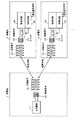
図9は、給電元と給電先が1対1で対応する磁界共鳴方式の非接触給電システムの構成例を示すブロック図である。図9に示した磁界共鳴方式の非接触給電システムは、給電元100と、給電先200とからなっている。 FIG. 9 is a block diagram illustrating a configuration example of a magnetic resonance type non-contact power feeding system in which a power feeding source and a power feeding destination correspond one-to-one. The magnetic resonance type non-contact power supply system shown in FIG. 9 includes a power supply source 100 and a power supply destination 200.
図9に示したように、例えば充電台である給電元100は、交流電源101、励振素子102、共鳴素子103を備えている。また、例えば、携帯電話端末などである給電先200は、共鳴素子201、励振素子202、整流回路203を備えている。
As shown in FIG. 9, for example, a power supply source 100 that is a charging stand includes an AC power source 10 1 , an excitation element 102, and a resonance element 103. In addition, for example, a power supply destination 200 such as a mobile phone terminal includes a resonance element 201, an excitation element 202, and a
給電元の励振素子102と共鳴素子103、及び、給電先の共鳴素子201と励振素子202とは、いずれも空芯コイルで構成されている。そして、給電元100の内部では、励振素子102と共鳴素子103とが電磁誘導により強く結合する構成となっている。同様に、給電先200の内部では、共鳴素子201と励振素子202とが電磁誘導により強く結合する構成となっている。 The feeding source excitation element 102 and the resonance element 103, and the feeding destination resonance element 201 and the excitation element 202 are all formed of air-core coils. In the power supply source 100, the excitation element 102 and the resonance element 103 are strongly coupled by electromagnetic induction. Similarly, in the power supply destination 200, the resonance element 201 and the excitation element 202 are strongly coupled by electromagnetic induction.
そして、給電元100の共鳴素子(空芯コイル)103と、給電先200の共鳴素子(空芯コイル)201の自己共鳴周波数(自己共振周波数)が一致したときに磁界共鳴関係になり、結合量が最大で、損失が最小となる。 When the resonance element (air-core coil) 201 of the power supply source 100 and the resonance element (air-core coil) 201 of the power supply destination 200 coincide with each other, the magnetic resonance relationship is established, and the coupling amount Is the largest and the loss is the smallest.
すなわち、図9に示した非接触給電システムにおいては、まず、給電元において、交流電源101からの所定周波数の交流電力(交流電流)が励振素子102に供給され、これが電磁誘導によって共鳴素子103へ交流電力を誘起させる。ここで、交流電源101において発生させる交流電力の周波数は、供給元の共鳴素子103と供給先の共鳴素子201との自己共鳴周波数と同一になるようにしている。
That is, in the non-contact power feeding system shown in FIG. 9, first, alternating current power (alternating current) of a predetermined frequency is supplied from the
そして、上述したように、給電元の共鳴素子103と給電先の共鳴素子201とは互いに磁界共鳴の関係に配置されており、共鳴周波数(共振周波数)において共鳴素子103から共鳴素子201へと非接触で交流電力が供給される。 As described above, the resonance element 103 that is the power supply source and the resonance element 201 that is the power supply destination are arranged in a magnetic resonance relationship with each other, and the resonance element 103 does not move from the resonance element 103 to the resonance element 201 at the resonance frequency (resonance frequency). AC power is supplied by contact.
給電先200において、給電元の共鳴素子103からの交流電力は、共鳴素子201により受け付けられる。共鳴素子201からの交流電力は、電磁誘導により励振素子2を通じて整流回路に供給され、ここで直流電力(直流電流)に変換されて出力される。 In the power supply destination 200, the AC power from the resonance element 103 as the power supply source is received by the resonance element 201. The AC power from the resonance element 201 is supplied to the rectifier circuit through the excitation element 2 by electromagnetic induction, and is converted into DC power (DC current) and output.
このようにして、給電元から給電先に対して、非接触で交流電力が供給するようにされる。なお、整流回路203から出力された直流電力は、例えば、バッテリが接続された充電回路に供給され、当該バッテリの充電に用いられるようにされる。
In this way, AC power is supplied from the power supply source to the power supply destination in a contactless manner. Note that the DC power output from the
そして、図9に示したように構成される給電元と給電先とが1対1に対応する非接触給電システムにおいては、以下のような特徴がある。 And in the non-contact electric power feeding system with which the electric power feeding source and electric power feeding destination comprised as shown in FIG. 9 respond | correspond one-to-one, there exist the following characteristics.
当該非接触給電システムにおいては、図10(A)に示すような交流電源の周波数と結合量の関係を有する。図10(A)を見ると分るように、交流電源の周波数が低かったり、逆に高かったりしても結合量は大きくならず、磁界共鳴現象を発生させる特定の周波数においてのみ、結合量が最大となる。すなわち、磁界共鳴により周波数選択性を示すことが分る。 The contactless power supply system has a relationship between the frequency of the AC power supply and the coupling amount as shown in FIG. As can be seen from FIG. 10A, even if the frequency of the AC power supply is low or conversely high, the amount of coupling does not increase, and the amount of coupling is only at a specific frequency that causes the magnetic resonance phenomenon. Maximum. That is, it can be seen that the magnetic field resonance exhibits frequency selectivity.
また、当該非接触給電システムにおいては、図10(B)に示すような共鳴素子103、201間の距離と結合量の関係を有する。図10(B)を見ると分かるように、共鳴素子間の距離が遠くなれば結合量は落ちる。 Further, the non-contact power feeding system has a relationship between the distance between the resonance elements 103 and 201 and the coupling amount as shown in FIG. As can be seen from FIG. 10B, the amount of coupling decreases as the distance between the resonant elements increases.
しかし、共鳴素子間の距離が近いからといって結合量が大きくなるわけではなく、ある共鳴周波数に於いて、結合量が最大となる距離が存在する。また、図10(B)から、共鳴素子間の距離がある程度の範囲であれば、一定以上の結合量を確保できることも分かる。 However, the amount of coupling does not increase just because the distance between the resonant elements is short, and there is a distance at which the amount of coupling is maximum at a certain resonance frequency. FIG. 10B also shows that a certain amount of coupling can be secured if the distance between the resonant elements is within a certain range.
また、当該非接触給電システムにおいては、図10(C)に示すような共鳴周波数と最大結合量が得られる共鳴素子間距離との関係を有する。すなわち、共鳴周波数が低いと共鳴素子間隔は広いことが分かる。また、共鳴周波数が高いと共鳴素子間隔を狭くすることによって最大結合量が得られることが分かる。 Further, the non-contact power supply system has a relationship between the resonance frequency and the distance between the resonance elements that provides the maximum coupling amount as shown in FIG. That is, it can be seen that the resonance element interval is wide when the resonance frequency is low. It can also be seen that when the resonance frequency is high, the maximum amount of coupling can be obtained by narrowing the interval between the resonance elements.
現在、既に広く用いられている電磁誘導方式の非接触給電システムでは、給電元と給電先とで磁束を共有する必要があり、効率良く電力を送るには給電元と給電先とを極近接して配置する必要があり、結合の軸合わせも重要である。 In the electromagnetic contact type non-contact power supply system that is already widely used, it is necessary to share the magnetic flux between the power supply source and the power supply destination, and in order to send power efficiently, the power supply source and the power supply destination are in close proximity. The alignment of the coupling is also important.
一方、磁界共鳴現象を用いた非接触給電システムでは、上述のように、磁界共鳴現象という原理から、電磁誘導方式よりも距離を離して電力伝送することができ、かつ、多少軸合わせが悪くても伝送効率があまり落ちないという利点がある。 On the other hand, in the non-contact power feeding system using the magnetic field resonance phenomenon, as described above, it is possible to transmit electric power at a greater distance than the electromagnetic induction method due to the principle of the magnetic field resonance phenomenon. However, there is an advantage that the transmission efficiency does not decrease so much.
以上のことをまとめると、図11に示すように、磁界共鳴型の非接触給電システムと、電磁誘導方式の非接触給電システムとでは、違いが存在する。そして、図11に示したように、磁界共鳴型の非接触給電システムの場合には、送受コイル(共鳴素子)間のずれにも強く、伝送距離を長くすることができる。 To summarize the above, as shown in FIG. 11, there is a difference between a magnetic resonance type non-contact power feeding system and an electromagnetic induction type non-contact power feeding system. As shown in FIG. 11, in the case of a magnetic resonance type non-contact power feeding system, the transmission distance can be increased and the transmission distance (resonance element) is strong.
このため、磁界共鳴型の非接触給電システムの場合には、図12に示すように、1台の給電元(充電台)に対して、複数の給電先(携帯端末)を載置して充電を行うようにすることができる。 For this reason, in the case of a magnetic resonance type non-contact power supply system, as shown in FIG. 12, a plurality of power supply destinations (mobile terminals) are placed and charged with respect to one power supply source (charging base). Can be done.
しかし、給電元(充電台)に載置される複数の給電先(携帯端末)の中には、他の給電先に優先して充電を迅速に行うようにしたいものもあれば、例えば、翌日の使用開始時までに充電が終わっていればよいというものもある。 However, some of the plurality of power supply destinations (portable terminals) placed on the power supply source (charging stand) want to be charged quickly in preference to other power supply destinations. In some cases, it is only necessary to finish charging before the start of use.
このように、複数の給電先に対して優先順位を付けて充電できるようにする従来の方式として、特許文献1には、いわゆる接触型の電池パック充電アダプタの発明が開示されている。
As described above,
この特許文献1に記載の電池パック充電アダプタは、1度に複数の電池パックに対して充電が可能なものであり、具体的構成の開示はないが、優先切替手段を備え、接続された電池パック毎に充電の優先順位がつけられる機能を有することが示唆されたものである。
The battery pack charging adapter described in
また、給電先に優先順位を付与するものではないが、非接触型の給電システムに関し、特許文献2には、いわゆる電磁誘導型の非接触携帯通信機器用充電装置に関する発明が開示されている。 Further, although priority is not given to a power supply destination, Patent Document 2 discloses an invention related to a so-called electromagnetic induction type charging device for a non-contact portable communication device.
この特許文献2に記載の携帯通信機器用充電装置は、充電中の携帯通信機器の通信動作に悪影響を及ぼすのを回避するため、携帯通信機器からの通信を行うタイミングを示す情報に基づいて、充電装置からの電力の供給のオン/オフを行う発明が開示されている。 In order to avoid adversely affecting the communication operation of the mobile communication device being charged, the charging device for mobile communication device described in Patent Document 2 is based on information indicating the timing of performing communication from the mobile communication device. An invention for turning on / off the supply of electric power from a charging device is disclosed.
この特許文献2に記載の発明の場合には、上述もしたように、給電先に優先順位を付与するものではないが、結果として充電装置が携帯通信機器の充電状態を制御することができるようになっている。 In the case of the invention described in Patent Document 2, as described above, priority is not given to the power supply destination, but as a result, the charging device can control the charging state of the portable communication device. It has become.
ところで、上述した特許文献1に記載の発明は、複数の電池パックが接続端子を通じて物理的に接続されて用いられる充電アダプタ側において、これに接続された電池パックに対する充電の優先順位を制御するというものである。
By the way, the invention described in
図9に示した構成を有する給電側(充電台)においては、これに載置される携帯電子機器毎に共鳴素子が設けられるわけではない。このため図9に示した構成の磁界共鳴型の非接触給電システムには、給電元100側において、給電先毎に給電を制御できる構成を設けることはできないので、特許文献1に記載の発明を適用することはできない。 In the power feeding side (charging stand) having the configuration shown in FIG. 9, a resonance element is not provided for each portable electronic device placed on the power feeding side (charging stand). For this reason, the magnetic resonance type non-contact power supply system having the configuration shown in FIG. 9 cannot be provided with a configuration that can control power supply for each power supply destination on the power supply source 100 side. It cannot be applied.
また、上述した特許文献2に記載の発明の場合にも、携帯通信端末側からの情報に基づいて、充電装置側で、給電のオン/オフを制御するようにしている。すなわち、特許文献2に記載の技術もまた、充電装置側で給電のオン/オフを制御しているので、結局、特許文献1に記載の技術と同様に、磁界共鳴型の非接触給電システムに適用することはできない。
In the case of the invention described in Patent Document 2 described above, on / off of power feeding is controlled on the charging device side based on information from the mobile communication terminal side. That is, since the technique described in Patent Document 2 also controls on / off of power feeding on the side of the charging device, the magnetic resonance type non-contact power feeding system is eventually the same as the technique described in
このように、給電元が図9に示したように1つの共鳴素子しか備えない磁界共鳴型の非接触給電システムの場合には、特許文献1や特許文献2に開示された従来の技術を用いては、給電元から給電先の給電状態を制御することができない。このため、磁界共鳴型の非接触給電システムの場合には、給電先毎に充電の優先順位を付すことができないという問題がある。
As described above, in the case of a magnetic resonance type non-contact power supply system in which the power supply source has only one resonance element as shown in FIG. 9, the conventional techniques disclosed in
以上のことに鑑み、この発明は、共鳴方式の非接触給電システムにおいて、1つの給電元から給電を受ける複数の給電先(非接触受電装置)毎に優先度を付し、この優先度に応じて給電元からの電力を受電することができるようにすることを目的する。 In view of the above, the present invention assigns a priority to each of a plurality of power supply destinations (non-contact power receiving devices) that receive power from one power supply source in a resonance-type non-contact power supply system, and according to this priority. It is intended to be able to receive power from a power supply source.
上記課題を解決するため、請求項1に記載の発明の非接触受電装置は、
給電元の共鳴素子から共鳴により非接触で交流電力の供給を受ける共鳴素子と、
前記共鳴素子から電磁誘導により交流電力の供給を受ける励振素子と、
前記励振素子からの交流電力から直流電力を生成して出力する整流回路と、
前記整流回路への交流電力の供給/非供給を切り換える切り換え回路と
を備える。
In order to solve the above-mentioned problem, a non-contact power receiving device according to
A resonance element that is supplied with AC power in a non-contact manner by resonance from a resonance element of a power supply source;
An excitation element that is supplied with AC power by electromagnetic induction from the resonance element;
A rectifier circuit that generates and outputs DC power from AC power from the excitation element;
A switching circuit for switching supply / non-supply of AC power to the rectifier circuit.
この請求項1に記載の発明の非接触受電装置によれば、共鳴現象を利用し、給電元の共鳴素子を通じて供給される交流電力を受電側の共鳴素子を通じて受け付け、これを当該共鳴素子と電磁結合される励振素子を介して整流回路に供給されるようになっている。 According to the contactless power receiving device of the first aspect of the present invention, using the resonance phenomenon, AC power supplied through the resonance element of the power supply source is received through the resonance element on the power receiving side, and this is received between the resonance element and the electromagnetic wave. It is supplied to the rectifier circuit via a coupled excitation element.
そして、切り換え回路が整流回路への交流電力の供給/非供給を切り換えることによって、非接触受電装置毎に、受電のタイミングを制御し、非接触受電装置毎に受電の態様を変えることができるようにされる。 The switching circuit switches between supply / non-supply of AC power to the rectifier circuit, so that the timing of power reception can be controlled for each non-contact power receiving device, and the mode of power reception can be changed for each non-contact power receiving device. To be.
これにより、非接触受電装置毎に、目的とする優先順位で、給電元から供給される電力を受電し、これを利用することができるようにされる。 As a result, for each non-contact power receiving device, the power supplied from the power supply source can be received and used in the target priority order.
共鳴方式の非接触受電システムの給電先となる各受電装置において、自機が目的とする優先順位に応じて、給電元から電力の供給を受けることができる。 Each power receiving device that is a power supply destination of the resonance-type non-contact power receiving system can receive power supply from the power supply source according to the target priority order.
以下、図を参照しながら、この発明による装置、方法の一実施の形態について説明する。この発明は、磁界共鳴方式、電界共鳴方式、電磁共鳴方式等の種々の共鳴方式に適用可能なものであるが、以下においては磁界共鳴方式を用いる場合を例にして説明する。 Hereinafter, an embodiment of an apparatus and a method according to the present invention will be described with reference to the drawings. The present invention can be applied to various resonance methods such as a magnetic field resonance method, an electric field resonance method, an electromagnetic resonance method, and the like. In the following, the case where the magnetic field resonance method is used will be described as an example.
[第1の実施の形態]
[磁界共鳴方式の非接触給電システム]
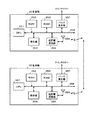
図1は、第1の実施の形態の磁界共鳴方式の非接触給電システムの構成例を説明するための図である。図1に示すように、この実施の形態の非接触給電システムは、給電元1と、複数の給電先2、3、…とからなっている。
[First Embodiment]
[Magnetic resonance type non-contact power feeding system]
FIG. 1 is a diagram for explaining a configuration example of a magnetic resonance type non-contact power feeding system according to a first embodiment. As shown in FIG. 1, the non-contact power feeding system of this embodiment includes a
給電元1は、いわゆる充電台の構成とされたものであり、例えば、図12に示したように、携帯電話端末などの給電先となる複数の非接触受電装置が載置可能な大きさを有するものである。
The
そして、給電先2、3、…のそれぞれは、上述のように、携帯電話端末などの給電先となる非接触受電装置であり、この発明による装置、方法の一実施の形態が適用されたものである。 Each of the power supply destinations 2, 3,... Is a non-contact power receiving device that is a power supply destination such as a mobile phone terminal, as described above, and to which an embodiment of the apparatus and method according to the present invention is applied. It is.
給電元1は、図1に示すように、交流電源11、励振素子12、共鳴素子13を備えたものである。一方、給電先2は、図1に示すように、共鳴素子21、励振素子22、スイッチ回路23、整流回路24、制御回路25を備えたものである。同様に、給電先3は、図1に示すように、共鳴素子31、励振素子32、スイッチ回路33、整流回路34、制御回路35を備えたものである。
As shown in FIG. 1, the
給電元1の励振素子12、共鳴素子13は、いずれも空芯コイルで構成されている。給電先2の共鳴素子21、励振素子22、及び、給電先3の共鳴素子31、励振素子32もまた、空芯コイルで構成されている。
Both the excitation element 12 and the
そして、供給元1の交流電源11は、供給元1の共鳴素子13、供給先2の共鳴素子21、供給先3の共鳴素子31の自己共鳴周波数(自己共振周波数)と同一、あるいは、略同一の周波数の交流電力(交流電流)を発生させて、これを励振素子12に供給する。
The
すなわち、図1に示した磁界共鳴型の非接触給電システムにおいて、供給元1の共鳴素子13、供給先2の共鳴素子21、供給先3の共鳴素子31のそれぞれは、同一、あるいは、略同一の共鳴周波数(共振周波数)を有するものである。
That is, in the magnetic field resonance type non-contact power feeding system shown in FIG. 1, the
また、供給元1の交流電源11は、目的とする周波数の交流電力を発生させるため、例えば、コルピッツ型発振回路やハートレ型発振回路などを含むものである。
Further, the
励振素子12は、交流電源11からの交流電力により励振されることにより、共鳴素子13に交流電力を供給する素子である。交流電源11からの交流電力の供給を受ける励振素子12と共鳴素子13とは電磁誘導により強く結合するようにされている。
The excitation element 12 is an element that supplies AC power to the
このため、交流電源11からの交流電力は、励振素子12を介して、共鳴素子13に供給される。なお、励振素子12は、交流電源11と共鳴素子13との間のインピーダンスの整合を取ることによって、電気信号の反射を防止する役割も果たす。
For this reason, AC power from the
共鳴素子13は、励振素子12から供給される交流電力により磁界を発生させるものである。共鳴素子13は、インダクタンス及びキャパシタンスを有する。共鳴素子13は、共鳴周波数において磁界強度が最も高くなる。
The
図8は、共鳴素子13の共鳴周波数frを求めるための式を示す図である。図8に示した式(1)において、文字Lは共鳴素子13の有するインダクタンスであり、文字Cは共鳴素子13の有するキャパシタンスである。
FIG. 8 is a diagram showing an equation for obtaining the resonance frequency fr of the
したがって、共鳴素子13の共鳴周波数は、共鳴素子13の有するインダクタンスLとキャパシタンスCとにより定まる。上述したように、共鳴素子13は、空芯コイルにより構成されるので、共鳴素子13の線間容量がキャパシタンスとしての役割を果たすことになる。そして、共鳴素子13は、コイルの軸方向に磁界を発生させる。
Therefore, the resonance frequency of the
供給先2の共鳴素子21と供給先3の共鳴素子31とは、磁界共鳴による磁界結合によって、供給元1からの交流電力の供給を受けるための素子である。供給先2の共鳴素子21と供給先3の共鳴素子31とは、図8の式(1)を用いて説明した給電元の共鳴素子13と同様に、インダクタンスLとキャパシタンスCを有し、給電元の共鳴素子13と同一、あるいは、略同一の共鳴周波数を有するものである。
The resonance element 21 of the supply destination 2 and the resonance element 31 of the supply destination 3 are elements for receiving supply of AC power from the
そして、上述したように、供給先2の共鳴素子21と供給先3の共鳴素子31とは、空芯コイルの構成とされているので、線間容量がキャパシタンスとしての役割を果たす。そして、図1に示したように、供給元1の共鳴素子13に対して、供給先2の共鳴素子21と供給先3の共鳴素子31とは磁界共鳴により接続される。
As described above, since the resonance element 21 of the supply destination 2 and the resonance element 31 of the supply destination 3 are configured as air-core coils, the capacitance between the lines plays a role as capacitance. As shown in FIG. 1, the resonance element 21 of the supply destination 2 and the resonance element 31 of the supply destination 3 are connected to the
これにより、共鳴周波数(共振周波数)において、給電元1の共鳴素子13から給電先2の共鳴素子21と給電先3の共鳴素子31とに対して、磁界共鳴により非接触で交流電力が供給される。
As a result, at the resonance frequency (resonance frequency), AC power is supplied from the
そして、上述したように、供給先2においては共鳴素子21と励振素子22とが電磁誘導により結合され、共鳴素子21から励振素子22を通じて交流電力が整流回路24に供給するようにされる。同様に、供給先3においては共鳴素子31と励振素子32とが電磁誘導により結合され、共鳴素子31から励振素子32を通じて交流電力が整流回路34に供給される。
As described above, at the supply destination 2, the resonance element 21 and the excitation element 22 are coupled by electromagnetic induction, and AC power is supplied from the resonance element 21 to the
なお、供給先2の励振素子22は、共鳴素子21と整流回路24との間のインピーダンスの整合を取ることによって、電気信号の反射を防止する役割も果たす。同様に、供給先3の励振素子32は、共鳴素子31と整流回路34との間のインピーダンスの整合を取ることによって、電気信号の反射を防止する役割も果たす。
The excitation element 22 of the supply destination 2 also plays a role of preventing reflection of the electric signal by matching the impedance between the resonance element 21 and the
そして、整流回路24、整流回路34からの直流電力は、図示しないが、バッテリが接続された充電回路に供給されて、バッテリの充電に用いられるようにされる。
The DC power from the
このように、この実施の形態の磁界共鳴方式の非接触給電システムにおいては、給電先2と給電先3とのそれぞれは、給電元1から非接触で電力の供給を受けて、これをバッテリの充電に用いるなどのことができるようにされる。
As described above, in the magnetic resonance type contactless power supply system of this embodiment, each of the power supply destination 2 and the power supply destination 3 receives power supply from the
そして、この実施の形態の磁界共鳴方式の非接触給電システムの給電先2は、励振素子22と整流回路24との間にスイッチ回路23を備えると共に、スイッチ回路23のオン/オフを制御する機能を有する制御回路25を備えている。
The power supply destination 2 of the magnetic field resonance type non-contact power supply system of this embodiment includes a
同様に、この実施の形態の磁界共鳴方式の非接触給電システムの給電先3は、励振素子32と整流回路34との間にスイッチ回路33を備えると共に、スイッチ回路33のオン/オフを制御する機能を有する制御回路35を備えている。
Similarly, the power supply destination 3 of the magnetic field resonance type non-contact power supply system of this embodiment includes a
そして、給電先2、給電先3のそれぞれは、充電処理に関し、優先モードと非優先モードとを備えている。ここで、優先モードは、スイッチ回路23、スイッチ回路33を常時オンにして、給電元1から電力の供給を常時受けるようにするものである。
Each of the power supply destination 2 and the power supply destination 3 has a priority mode and a non-priority mode regarding the charging process. Here, in the priority mode, the
また、非優先モードは、例えば、1秒間で300ミリ秒だけスイッチ回路23、スイッチ回路33をオンにするというように、所定の単位時間において、その単位時間よりも短い予め決められた一定時間分だけ、給電元1から電力の供給を受けるものである。
In the non-priority mode, for example, the
そして、給電先2、給電先3のユーザーは、充電に先立ち、給電先2、給電先3のそれぞれに対し、図示しない操作部を通じて優先モードとするか、非優先モードとするかの設定入力を行う。 Then, before charging, the users of the power supply destination 2 and the power supply destination 3 enter a setting input for setting the priority mode or the non-priority mode for each of the power supply destination 2 and the power supply destination 3 through an operation unit (not shown). Do.
当該設定入力は、制御部25、制御部35により受け付けられる。そして、制御部25、制御部35は、設定されたモードに従って、スイッチ回路23、スイッチ回路33のオン/オフを制御する。
The setting input is accepted by the
例えば、給電先2が優先モードに設定され、給電先3が非優先モードに設定されたとする。この場合、給電先2の制御部25は、スイッチ回路23を常時オンにするように制御する。一方、給電先3の制御部35は、例えば、1秒間毎に300ミリ秒間だけ、スイッチ回路33をオンにし、それ以外のときには、スイッチ回路33をオフにするように制御する。
For example, assume that the power supply destination 2 is set to the priority mode and the power supply destination 3 is set to the non-priority mode. In this case, the
これにより、供給先2は、自機のスイッチ回路23がオンであり、供給先3のスイッチ回路33がオフのときには、自機だけが供給元1からの電力の供給を受けて、優先的に充電を行うようにすることができる。
As a result, when the
また、給電先2は、自機のスイッチ回路23がオンであり、供給先3のスイッチ回路33もまたオンである場合にも、給電元1から電力の供給を受ける。この場合、給電先2だけでなく、給電先3もまた給電元1から電力の供給を受けることにより、給電先2における給電元1からの電力の受電量は減る。しかし、給電先2は、給電元1からの電力の供給は継続して受けることができる。
In addition, the power supply destination 2 receives power supply from the
これに対して、供給先3は、自機のスイッチ回路33がオフのときには、供給元1からの電力の供給を受けることはない。しかし、供給先3は、自機のスイッチ回路33がオンのときには、供給元1から電力の供給を受けることができるようにされる。
On the other hand, the supply destination 3 does not receive power supply from the
なお、上述したように、給電先2のスイッチ回路23は常時オンにされている。このため、給電先3のスイッチ回路33がオンのときには、供給先2のスイッチ回路23もオンとなっており、給電先2、給電先3とも電力の供給を受けるので、給電先2、給電先3のそれぞれの受電量は減る。しかし、上述もしたように、給電先2、給電先3のそれぞれは、電力の供給は継続して受けることができる。
As described above, the
このように、充電処理に関し、優先モードとされた供給先2においては、スイッチ回路23が常時オンにされる。そして、給電先2においては、自機のスイッチ回路23のみがオンになっている期間においては、優先的に供給元1からの給電を受けることができるようにされ、充電も迅速になされる。
In this way, with respect to the charging process, the
また、充電処理に関し、非優先モードとされた供給先3においては、スイッチ回路33が単位時間当たりにおいて、所定の時間しかオンにされないので、優先モードとされた給電先2よりは、給電元1から給電を受ける時間が短くなる。
Regarding the charging process, in the supply destination 3 set in the non-priority mode, the
しかし、スイッチ回路33がオンにされている間においては、給電元1から給電を受けることができるようにされるので、優先モードの給電先2よりは、充電に時間がかかるものの、給電元1から給電を受けて充電を行うことができるようにされる。
However, while the
なお、上述した例においては、給電先2を優先モードとし、給電先3を非優先モードとしたが、これに限るものではない。給電先3を優先モードとし、給電先2を非優先モードとすることもできる。 In the example described above, the power supply destination 2 is set to the priority mode and the power supply destination 3 is set to the non-priority mode. However, the present invention is not limited to this. The power supply destination 3 can be set to the priority mode, and the power supply destination 2 can be set to the non-priority mode.
また、給電先2と給電先3のいずれをも優先モードとすることもできる。この場合には、給電先2のスイッチ回路23も、給電先3のスイッチ回路33もオンとなるようにされるので、給電先2と給電先3とに給電が行うようにされる。
Further, both the power supply destination 2 and the power supply destination 3 can be set to the priority mode. In this case, since both the
しかし、給電先が増えた場合、上述もしたように、各給電先における給電元1からの電力の受電量は減ることになり、充電の効率は落ちることになる。しかし、給電先2、給電先3においては、常時供給元1から給電を受けることにより、双方が常時充電を行うことができるようにされる。
However, when the number of power supply destinations increases, as described above, the amount of power received from the
また、給電先2と給電先3のいずれをも非優先モードとすることもできる。この場合には、給電先2は自機のスイッチ回路23がオンにされたときにおいてのみ、また、給電先3は自機のスイッチ回路33がオンされたときにおいてのみ、給電元1からの給電を受けることができる。したがって、双方とも、優先モード時よりも充電に長時間を要することになる。
Further, both the power supply destination 2 and the power supply destination 3 can be set to the non-priority mode. In this case, the power supply destination 2 is supplied from the
このように、給電元1に特別な回路を設けることなく、給電先2のスイッチ回路23と、給電先3のスイッチ回路33とを、優先モードとされたか、非優先モードとされたかにおじて、オン/オフを制御できるようにする。これにより、給電先において、充電処理に関し、優先/非優先の区別を設けて、充電を行うようにすることができる。
Thus, without providing a special circuit at the
なお、この第1の実施の形態においては、給電先は、給電先2と給電先3との2つである場合を例にして説明したが、これに限るものではない。給電先は、2つ以上の複数であってもよい。 In the first embodiment, the case where there are two power supply destinations, ie, the power supply destination 2 and the power supply destination 3, has been described as an example. However, the present invention is not limited to this. The power supply destination may be two or more.
また、充電処理に関するモードも、優先モードと非優先モードとの2つではなく、さらに複数のモードを用いるようにしてもよい。例えば、最優先モード、優先モード、非優先モードなどのように複数のモードを設ける。 Also, the modes related to the charging process are not limited to the priority mode and the non-priority mode, and a plurality of modes may be used. For example, a plurality of modes such as a highest priority mode, a priority mode, and a non-priority mode are provided.
そして、最優先モード、優先モード、非優先モードの順に、整流回路に交流電力を供給するか否かを切り換えるスイッチ回路がオンとなる時間が短くなるように制御する。逆に言えば、整流回路に交流電力を供給するか否かを切り換えるスイッチ回路をオンにする時間が、最優先モードが一番長く、次に、優先モードが長く、非優先モードが一番短いと言うようにする。 Then, in order of the highest priority mode, the priority mode, and the non-priority mode, control is performed so that the time during which the switch circuit for switching whether or not to supply AC power to the rectifier circuit is turned on becomes shorter. In other words, the time to turn on the switch circuit that switches whether or not to supply AC power to the rectifier circuit is the longest in the highest priority mode, next the longest priority mode, and the shortest non-priority mode To say.
これにより、給電先において、充電処理に関し、各給電先に優先度を付与することができるようにされる。 Thereby, in the power supply destination, priority can be given to each power supply destination regarding the charging process.
[第2の実施の形態]
ところで、上述した第1の実施の形態の場合、複数の給電先において、整流回路に交流電力を供給するか否かを切り換えるスイッチ回路がいずれもオンになった場合には、各給電先における受電量が低下する。このため、優先度に応じて想定した充電時間よりも、実際の充電時間の方が長くかかってしまうといったことも発生する可能性がある。
[Second Embodiment]
By the way, in the case of 1st Embodiment mentioned above, when all the switch circuits which switch whether alternating current power is supplied to a rectifier circuit in a some electric power feeding destination are turned on, the electric power receiving in each electric power feeding destination The amount is reduced. For this reason, the actual charging time may take longer than the charging time assumed according to the priority.
そこで、この第2の実施の形態においては、各給電先において、自機が給電元から給電を受けている場合には、他の給電先においては給電を受けないようにして、給電元からの受電量が低下しないように制御できるようにしたものである。換言すれば、各給電先において、排他的に給電を受けることができるようにするものである。 Therefore, in the second embodiment, when the power supply receives power from the power supply source at each power supply destination, the power supply is not received from other power supply destinations. The control is made so that the amount of power received does not decrease. In other words, each power supply destination can receive power exclusively.
なお、この第2の実施の形態の装置、方法もまた、図1に示した磁界共鳴方式の非接触給電システムと同様の構成を有する非接触給電システムの給電先に適用されるものである。このため、この第2の実施の形態の磁界共鳴方式の非接触給電システムは、図1に示した磁界共鳴方式の非接触給電システムと同様の構成を有するものとして、図1をも参照しながら説明する。 The apparatus and method of the second embodiment are also applied to the power supply destination of the non-contact power supply system having the same configuration as the magnetic resonance type non-contact power supply system shown in FIG. For this reason, the magnetic resonance type non-contact power feeding system of the second embodiment has the same configuration as the magnetic field resonance type non-contact power feeding system shown in FIG. explain.
この第2の実施の形態の磁界共鳴方式の非接触給電システムにおいても、給電元1から給電先2と給電先3とが給電を受けるが、一方が給電を受けている場合には他方は給電を受けないように、排他的に給電期間を制御することができるものである。
Also in the magnetic resonance type non-contact power feeding system of the second embodiment, the
図2は、この第2の実施の形態の磁界共鳴方式の非接触給電システムにおいて、給電先2と給電先3とが給電元1から給電を受ける場合の具体的な態様の一例について説明するための図である。
FIG. 2 is a diagram for explaining an example of a specific mode in the case where the power supply destination 2 and the power supply destination 3 receive power supply from the
この第2の実施の形態の非接触給電システムでは、各給電先において、充電に関する優先度を、例えばパーセンテージや割合により設定することができるようにされているとする。 In the non-contact power feeding system of the second embodiment, it is assumed that the priority related to charging can be set by, for example, a percentage or a ratio at each power feeding destination.
そして、給電先2と給電先3とにおいて、充電に関する優先度が、例えば共に50%であるとする。この場合、図2(A)に示すように、デューティ比が50%となり、相互にオンになる期間が重ならないように、給電先2と給電先3とのそれぞれにおいて、スイッチ回路23、スイッチ回路33のオン/オフを制御するためのパルス信号を生成する。
In the power supply destination 2 and the power supply destination 3, it is assumed that the priorities for charging are both 50%, for example. In this case, as shown in FIG. 2A, the
また、給電先2の充電に関する優先度が60%であり、給電先3の充電に関する優先度が40%であるとする。この場合、図2(B)に示すように、デューティ比が60%となるスイッチ回路23用のパルス信号と、デューティ比が40%となるスイッチ回路33用のパルス信号とを、相互にオンになる期間が重ならないように生成する。
Further, it is assumed that the priority regarding charging of the power supply destination 2 is 60% and the priority regarding charging of the power supply destination 3 is 40%. In this case, as shown in FIG. 2B, the pulse signal for the
また、給電先2の充電に関する優先度が90%であり、給電先3の充電に関する優先度が10%であるとする。この場合、図2(C)に示すように、デューティ比が90%となるスイッチ回路23用のパルス信号と、デューティ比が10%となるスイッチ回路33用のパルス信号とを、相互にオンになる期間が重ならないように生成する。
Further, it is assumed that the priority regarding charging of the power supply destination 2 is 90% and the priority regarding charging of the power supply destination 3 is 10%. In this case, as shown in FIG. 2C, the pulse signal for the
このように、この第2の実施の形態の非接触給電システムにおいては、スイッチ回路23、33のオンになる期間が重複することがないようにする。これにより、それぞれの給電先において自機が給電を受ける場合に、その受電量が減少するのを防止し、想定通りに効率よく給電元1からの電力を受電して、充電を行うことができるようにしている。
As described above, in the non-contact power feeding system according to the second embodiment, the periods during which the
そして、図2に示したように、各給電先において、給電期間(受電期間)が重複することがないようにするために、この第2の実施の形態の非接触給電システムにおいては、各給電先間において通信を行って、給電期間を排他的に設定できるようにしている。 As shown in FIG. 2, in the non-contact power feeding system according to the second embodiment, the power feeding periods (power receiving periods) do not overlap at each power feeding destination. Communication is performed between the destinations so that the power supply period can be set exclusively.
図3は、図1に示した給電先2のスイッチ回路23を制御する制御部25と給電先3のスイッチ回路33を制御する制御部35の構成例を説明するためのブロック図である。
FIG. 3 is a block diagram for explaining a configuration example of the
図3に示すように、給電先2の制御部25は、CPU251、ROM252、RAM253、操作部254、近距離通信部255、パルス発生器257がCPUバス258を通じて接続されて構成されたものである。また、近距離通信部255には、送受信用のアンテナ256が接続されている。
As shown in FIG. 3, the
CPU251は、後述するROM252に記憶保持されているプログラムを読み出して実行し、後述する操作部254や近距離通信部255からの情報を処理したり、後述する近距離通信部255やパルス発生器257を制御したりする。
CPU251 reads out and executes a program stored and held in the ROM252 to be described later, or to process the information from the
また、ROM252は、上述したように、CPU251によって実行されるプログラムや処理に必要になるデータなどが記憶されたものである。RAM253は、CPU251によって実行される処理の途中結果を一時記憶するなど、主に作業領域として用いられるものである。
Further, as described above, the
そして、操作部254は、この第2の実施の形態においては、主に、充電処理に関し、充電の優先度を示すユーザーからの情報の入力を受け付けて、これをCPU251に通知する機能を有する。
And in this 2nd Embodiment, the
近距離通信部255は、数十センチ程度の近距離通信が可能なものであり、送受信アンテナ256を通じて、近隣の給電先との間で通信を行うことができるものである。したがって、近距離通信部255は、近隣の給電先からの情報を受信してCPU251に通知したり、CPU251の制御に応じて、自機から近隣の給電先に情報を送信したりする。
The short-
なお、近距離通信部255は、例えば、IEEE802.15、Bluetooth、ISO/IEC18092等の規格のものである。もちろん、これらの規格のものに限るものではなく、種々の規格のものを用いることができる。
Note that the short-
パルス発生器257は、CPU251の制御に応じて、図1に示したスイッチ回路23のオン/オフを制御するためのパルス信号を発生させる。すなわち、パルス発生器257が、CPU251の制御に応じて、図2を用いて説明したようなスイッチ回路23を制御するためのパルス信号を発生させる。
The
そして、図3に示したように、給電先3の制御部35もまた、給電先2の制御部25と同様の構成を有する。すなわち、給電先3の制御部35のCPU351、ROM352、RAM353は、給電先2の制御部25のCPU251、ROM252、RAM253と同様に構成されたものである。
As shown in FIG. 3, the
また、給電先3の制御部35の操作部354、近距離通信部355及び送受信アンテナ356、パルス発生器357は、給電先2の制御部25の近距離通信部255及び送受信アンテナ256、パルス発生器257と同様に構成されたものである。また、給電先3の制御部35のCPUバス358は、給電先2の制御部25のCPUバス258と同様に各部を接続するバスである。
The
そして、給電先2は、操作部254を通じて充電処理に関する優先度を例えばパーセンテージで入力し、充電モードにした後に、給電元1に載置する。同様に、給電先3は、操作部354を通じて充電処理に関する優先度を例えばパーセンテージで入力し、充電モードにした後に、給電元1に載置する。
Then, the power supply destination 2 inputs the priority related to the charging process, for example, as a percentage through the
すると、給電先2のCPU251と給電先3のCPU351とのそれぞれは、後述する充電処理プログラムを実行する。そして、詳しくは後述するが、いずれかがホスト装置として機能して、他機の優先度を収集する。
Then, each of the
この後、ホスト装置として機能する給電先が、自機及び他機の優先度に応じて、自機及び他機においてどのようなパルス信号を生成するかを決定して、自機と他機に通知すると共に、自機と他機とにパルスの発生タイミングをも指示する。 After that, the power supply destination functioning as the host device determines what kind of pulse signal is to be generated in the own device and the other device according to the priority of the own device and the other device. In addition to informing, the own machine and the other machine are also instructed the pulse generation timing.
このようにして、給電先2、給電先3のそれぞれが、自機だけが給電を受けることができる期間を相互に設けて、適切に充電を行うことができるようにされる。 In this way, each of the power supply destination 2 and the power supply destination 3 can be appropriately charged by providing a period in which only the own device can receive power supply.
次に、この第2の実施の形態の給電先2、給電先3において、充電時に行われる処理の詳細を図4、図5のフローチャートを参照しながら説明する。すなわち、図4、図5は、給電先2、給電先3において、充電時に実行される処理(充電処理プログラム)の詳細を説明するためのフローチャートである。 Next, details of processing performed at the time of charging in the power supply destination 2 and the power supply destination 3 of the second embodiment will be described with reference to the flowcharts of FIGS. 4 and 5. That is, FIG. 4 and FIG. 5 are flowcharts for explaining details of processing (charging processing program) executed at the time of charging at the power supply destination 2 and the power supply destination 3.
なお、図4、図5に示す処理は、給電先2、給電先3で共通に行われる処理であるので、ここでは説明を簡単にするため、給電先2において実行される場合を例にして説明する。 The processes shown in FIGS. 4 and 5 are processes performed in common by the power supply destination 2 and the power supply destination 3, and here, in order to simplify the description, the case where the processes are executed in the power supply destination 2 is taken as an example. explain.
給電先2において、操作部254を通じて充電処理に関する優先度を示す情報の入力を受け付けた後、充電モードにする操作を受け付けると、CPU251は、ROM252から図4、図5に示す充電処理プログラムを読み出して、これを実行する。
When the power supply destination 2 receives an input of information indicating the priority related to the charging process through the
まず、CPU251は、近距離通信部255を制御し、他機から送信されてくる優先度情報送信要求を受信する処理を行う(ステップS1)。
First, the
そして、CPU251は、近距離通信部255からの情報を参照するようにして、優先度情報送信要求を受信したか否かを判断する(ステップS2)。このステップS2の判断処理は、自機よりも先にホスト機器となった給電先が存在するか否かを判断する処理である。
Then, the
ステップS2の判断処理において、優先度情報送信要求を受信していないと判断したときには、まだホスト機器になった給電先は存在していないので、CPU251は自機をホスト機器として特定する(ステップS3)。
If it is determined in step S2 that the priority information transmission request has not been received, the power supply destination that has become the host device does not yet exist, and therefore the
この後、CPU251は、例えば自機の識別情報を含む優先度情報送信要求を形成し、これを近距離通信部255及び送受信アンテナ256を通じて近隣に存在する可能性のある他の給電先に対して送信する(ステップS4)。
Thereafter, the
そして、CPU251は、近距離通信部255を制御して、ステップS4で送信した優先度情報送信要求に応じて他の給電先から送信されてくる優先度情報の受信処理を行う(ステップS5)。
Then, the
この後、CPU251は、他の給電先からの優先度情報を受信したか否かを判断する(ステップS6)。なお、他の給電先からの優先度情報には、送信元の給電先の識別情報等を含むものである。
Thereafter, the
ステップS6において、他の給電先からの優先度情報を受信したと判断したときには、CPU251は、自機と他の給電先とのそれぞれのパルス情報を生成し、自機に設定すると共に、近距離通信部255を通じて他の給電先に送信する(ステップS7)。
When it is determined in step S6 that priority information from another power supply destination has been received, the
すなわち、ステップS7では、新たな給電先からの優先度情報を受信するたびに、自機の優先度情報と、既に受信している他の給電先からの優先度情報と、新たに受信した他の給電先の優先度情報とに基づいて、自機及び他の給電先に対するパルス情報を生成する。 That is, in step S7, every time priority information from a new power supply destination is received, the priority information of the own device, priority information from other power supply destinations already received, and newly received other information Based on the priority information of the power supply destination, pulse information for the own device and other power supply destinations is generated.
そして、ステップS7では、自機用のパルス情報は自機に設定し、他の給電先に対するパルス情報は、近距離通信部255及び送受信アンテナ256を通じて、給電先毎に対応するパルス情報を送信する。
In step S7, the pulse information for the own device is set in the own device, and the pulse information for the other power supply destination is transmitted as the pulse information corresponding to each power supply destination through the short-
換言すれば、CPU251は、自機、及び、給電先毎のパルス情報を生成し、自機用のパルス情報は自機に設定し、他の給電先のパルス情報は、対応する給電先に送信することになる。
In other words, the
なお、パルス情報は、どのようなパルス信号を生成するかを示す情報であり、例えば、図2を用いて説明したように、デューティ比50%の(最初の5クロック分の期間をオンにし、次の5クロック分の期間はオフにする)パルス信号を生成するなどの情報である。 The pulse information is information indicating what kind of pulse signal is generated. For example, as described with reference to FIG. 2, the duty ratio is 50% (the period for the first five clocks is turned on, This is information such as generating a pulse signal).
この後、CPU251は、近距離無線通信部255を制御して、パルス信号の発生タイミングを示す情報を送信する(ステップS8)。そして、CPU251は、当該タイミングで自機においても、パルス信号発生部257を制御し、自機用のパルス情報に応じたパルス信号を生成して、これをスイッチ回路23に供給する。
Thereafter, the
これにより、CPU251は、自機のパルス情報に応じて適切なパルス信号を生成して、スイッチ回路23のオン/オフを制御し、排他的に給電元1から給電を受けて充電を開始する(ステップS9)。
Thereby, CPU251 produces | generates a suitable pulse signal according to the pulse information of an own machine, controls on / off of the
一方、ステップS6判断処理において、他の給電先からの優先度情報を受信していないと判断したときには、自機以外に給電先は存在しないと判断し、自機は既に充電を開始しているか否かを判断する(ステップS10)。 On the other hand, if it is determined in step S6 that the priority information from another power supply destination has not been received, it is determined that there is no power supply destination other than the own device, and has the device already started charging? It is determined whether or not (step S10).
ステップS10の判断処理において、充電未開始と判断した場合、CPU251は、パルス発生部257により常時オンとなる信号を発生させ、これをスイッチ回路23に供給し、自機が常時給電元1からの給電を受けて充電を行うようにする(ステップS11)。
If it is determined in step S10 that charging has not started, the
そして、ステップS9とステップS11の処理の後、及びステップS10の判断処理において、既に充電開始済みであると判断したときには、CPU251は、ステップS4からの処理を繰り返す。これにより、新たな給電先が給電元1に載置された場合にも対応できるようにする。
Then, after determining that charging has already started after the processing of step S9 and step S11 and in the determination processing of step S10, the
すなわち、ステップS4からの処理が繰り返し行われることにより、新たな給電先が給電元1に載置された場合にも、その新たな給電先の優先度情報をも考慮して、自機及び他の給電先に対するパルス情報を生成し直して配布することができる。
That is, by repeatedly performing the processing from step S4, even when a new power supply destination is placed on the
これにより、給電先が増えても、各給電先の優先度に応じて、各給電先のスイッチ回路を適切に制御し、各給電先が排他的に給電元1からの給電を受ける期間を設けることができるようにされる。
Thereby, even if the number of power supply destinations increases, according to the priority of each power supply destination, the switch circuit of each power supply destination is appropriately controlled, and each power supply destination is provided with a period for receiving power from the
一方、ステップS2の判断処理において、優先度情報送信要求を受信したと判断したときには、既にホスト機器となり優先度情報送信要求を送信している給電先が存在しているので、図5の処理に進む。 On the other hand, when it is determined in step S2 that the priority information transmission request has been received, there is already a power supply destination that has become the host device and transmits the priority information transmission request. move on.
そして、CPU251は、ホスト機器となっている要求元に対して既に自機の優先度情報を、送信済みか否かを判断する(ステップS12)。このステップS12の判断は、自機が優先度情報を送信した相手先と送信時間などの優先度情報の送信先履歴を保持しておくことにより判断することができる。
Then, the
ステップS12の判断処理において、当該要求元に対して、自機の優先度情報を送信していないと判断したときには、CPU251は、近距離通信部255を制御し、例えば、RAM253に設定されている自機の優先度情報を要求元に送信する(ステップS13)。なお、ステップS13において送信した優先度情報は、送信元の識別情報等の必要な情報が付加したものである。
In the determination process of step S12, when determining that the priority information of the own device is not transmitted to the request source, the
この後、図4のステップS7において説明したように、ホスト機器から送信されてくる自機宛のパルス情報を受信して自機のRAM253に設定する(ステップS14)。そして、図4のステップS8において説明したように、ホスト機器から送信されてくるパルス発生タイミングを受信するまで待ち状態となる(ステップS15)。
Thereafter, as described in step S7 of FIG. 4, pulse information addressed to the own device transmitted from the host device is received and set in the
ステップS15の判断処理において、パルス発生タイミングを受信したと判断したときには、CPU251は、ステップS14において設定したパルス情報に応じて、パルス発生器257を制御してパルスを発生させ、充電を開始させる(ステップS16)。
If it is determined in step S15 that the pulse generation timing has been received, the
すなわち、ステップS16においては、自機宛のパルス情報に応じたパルス信号がパルス発生器257により生成され、これがスイッチ回路23に供給されて、そのオン/オフが制御され、オン時において給電を受けて充電を行うことができるようにされる。
That is, in step S16, a pulse signal corresponding to the pulse information addressed to itself is generated by the
このステップS16の処理の後、CPU251は、図4のステップS1からの処理を繰り返し、ホスト機器が充電を完了して給電元1からはずされた場合も想定し、各給電先の優先度に応じた充電を常時適正に行うことができるようにされる。
After the process of step S16, the
また、ステップS12の判断処理において、当該要求元に対して、自機の優先度情報を送信済みであると判断したときには、CPU251は、自機宛の新たなパルス情報を、近距離通信部255を通じて受信したか否かを判断する(ステップS17)。
If it is determined in step S12 that the priority information of the own device has already been transmitted to the request source, the
ステップS17の判断処理において、自機宛の新たなパルス情報を受信したと判断したときには、当該新たなパルス情報をRAM253に設定し直し(ステップS18)、ステップS15からの処理を繰り返す。 If it is determined in step S17 that new pulse information addressed to the own device has been received, the new pulse information is reset in the RAM 253 (step S18), and the processing from step S15 is repeated.
また、ステップS17の判断処理において、自機宛の新たなパルス情報を受信していない判断したときには、ホスト装置の変更はないので、図4のステップS1からの処理を繰り返す。 If it is determined in step S17 that new pulse information addressed to the own device has not been received, the host device is not changed, and the processing from step S1 in FIG. 4 is repeated.
このように、図4、図5を用いて説明した処理を、各給電先の制御部において実行されることにより、各給電先の充電処理に関する優先度に応じパルス情報をホスト機器が生成して各給電先に配布することができる。 In this way, the processing described with reference to FIGS. 4 and 5 is executed by the control unit of each power supply destination, so that the host device generates pulse information according to the priority regarding the charging process of each power supply destination. It can be distributed to each power supply destination.
また、ホスト機器が、パルス発生タイミングをも供給するので、各給電先においてパルス信号の発生タイミングを統一することもできるので、各給電先において、自機だけが排他的に給電を受けることができる期間を設けて、給電を受け充電を行うことができる。 In addition, since the host device also supplies the pulse generation timing, it is possible to unify the generation timing of the pulse signal at each power supply destination, so that only the own device can receive power exclusively at each power supply destination. A period can be provided to receive power and perform charging.
なお、通常、給電元1に載置する各給電先のユーザーは単独のユーザーである場合が多いので、各機器の優先度の設定を間違えることは少ないと考えられる。しかし、例えば、複数の給電先がいずれも優先度100%であったり、各給電先の優先度を合わせると100%を超えたりした場合には、ホスト機器となった給電先が警告音と警告メッセージを出力し、ユーザーに優先度の設定の修正を促すようにすることができる。
Normally, each power supply destination user placed on the
また、警告を発することなく、ホスト機器となった給電先が、各給電先の優先度にもとづいて、優先度を自動修正するようにしてもよい。例えば、複数の給電先がいずれも優先度100%であった場合には、いずれの機器も均等にオン/オフ期間を有するが、その発生タイミングを異なるようにすることができる。 In addition, the power supply destination that has become the host device may automatically correct the priority based on the priority of each power supply destination without issuing a warning. For example, when all of the plurality of power supply destinations have a priority of 100%, all the devices have equal on / off periods, but the generation timing can be made different.
また、各給電先の優先度を合わせると100%を超えた場合には、各給電先の優先度に応じて、100%を超えないように、各給電先の優先度を自動調整することも可能である。 In addition, when the priority of each power supply destination exceeds 100%, the priority of each power supply destination may be automatically adjusted according to the priority of each power supply destination so that it does not exceed 100%. Is possible.
また、図4、図5に示した処理においては、ホスト装置が給電元1から外されてホスト装置が変わったり、新たな給電先が給電元1に載置されたりする点については考慮した。しかし、ホスト装置以外の給電先が、例えば、充電途中で給電元1から外される場合もある。
In the processing shown in FIGS. 4 and 5, the host device is removed from the
そこで、ホスト機器以外の給電先は、ホスト機器からの要求に応じて定期的に自機の優先度情報を送信し、ホスト機器はこれを受信して、給電元1に載置されている給電先に変更があったことを検出した場合に、パルス情報を生成し直すようにすることもできる。
Accordingly, a power supply destination other than the host device periodically transmits priority information of the own device in response to a request from the host device, and the host device receives this information and supplies power to the
このように、この第2の実施の形態の非接触給電システムに場合には、給電先間で通信を行うことにより、各給電先において、給電を受ける期間が重複することがないようにして、各給電先の優先度に応じて給電元1から給電を受けて充電を行うようにする事ができる。
Thus, in the case of the contactless power supply system of the second embodiment, by performing communication between the power supply destinations, in each power supply destination, the period of receiving power supply does not overlap, Charging can be performed by receiving power from the
なお、図4、図5を用いて説明した処理は、各給電先が排他的に給電期間を設けるようにする場合の一例であり、他の種々の方法を用いるようにすることももちろんできる。要は、複数の給電先が一度に給電元1に載置された場合に、充電量の減少を招くことなく、優先度に応じた適切な期間分ずつ給電を受けて、適切に充電を行えるようにする種々の方法を用いることが可能である。
Note that the processing described with reference to FIGS. 4 and 5 is an example in which each power supply destination is exclusively provided with a power supply period, and other various methods can be used as a matter of course. In short, when a plurality of power supply destinations are mounted on the
[第3の実施の形態]
上述した第1、第2の実施の形態の非接触給電システムにおいては、例えば、携帯電話端末などの給電先自体が、共鳴素子、励振素子、スイッチ回路、整流回路、制御回路を備えていた。
[Third Embodiment]
In the contactless power supply systems of the first and second embodiments described above, for example, a power supply destination such as a mobile phone terminal includes a resonance element, an excitation element, a switch circuit, a rectifier circuit, and a control circuit.
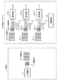
しかし、非接触で給電を受ける上述した構成を有していない従来からの種々の携帯機器も存在する。そこで、この第3の実施の形態の非接触給電システムは、給電元1と、アダプタの構成とされた給電先4とから構成され、給電先4から各携帯機器に対して電力を供給できる構成としたものである。
However, there are various conventional portable devices that do not have the above-described configuration for receiving power without contact. Therefore, the non-contact power supply system according to the third embodiment is configured by a
そして、アダプタの構成とされた給電先4を通じて、後述もするように、複数の携帯機器等に電力を供給することができるようにされる。また、この第3の実施の形態の給電先4は、第2の実施の形態の場合と同様に、携帯機器毎に充電処理に関して優先度を設定し、当該優先度に応じて、これに接続された携帯機器等に電力の供給ができるものである。 Then, as will be described later, power can be supplied to a plurality of portable devices and the like through the power supply destination 4 configured as an adapter. Moreover, the power supply destination 4 of this 3rd Embodiment sets the priority regarding a charge process for every portable apparatus similarly to the case of 2nd Embodiment, and connects to this according to the said priority It is possible to supply power to a portable device or the like.
図6は、この第3の実施の形態の非接触給電システムを説明するための図である。図6に示すように、給電元1は、図1に示した第1、第2の実施の形態の給電元1と同様に構成されたものである。
FIG. 6 is a diagram for explaining the non-contact power feeding system according to the third embodiment. As shown in FIG. 6, the
このため、図6において、図1に示した非接触給電システムと同様に構成される給電元1の各分には、図1と同じ参照符号を付し、その部分の説明については省略する。
For this reason, in FIG. 6, the same reference numerals as those in FIG. 1 are assigned to the parts of the
そして、この第3の実施の形態の給電先4は、3つの給電系を備えたものである。すなわち、第1の給電系は、共鳴素子41(a)、励振素子42(a)、スイッチ回路43(a)、整流回路44(a)からなる部分である。 The power supply destination 4 of the third embodiment is provided with three power supply systems. That is, the first power feeding system is a part including the resonance element 41 (a), the excitation element 42 (a), the switch circuit 43 (a), and the rectification circuit 44 (a).
また、第2の給電系は、共鳴素子41(b)、励振素子42(b)、スイッチ回路43(b)、整流回路44(b)からなる部分であり、第3の給電系は、共鳴素子41(c)、励振素子42(c)、スイッチ回路43(c)、整流回路44(c)からなる部分である。 The second power supply system is a part including the resonance element 41 (b), the excitation element 42 (b), the switch circuit 43 (b), and the rectifier circuit 44 (b), and the third power supply system is a resonance element. This is a portion composed of an element 41 (c), an excitation element 42 (c), a switch circuit 43 (c), and a rectifier circuit 44 (c).
そして、図6に示したように、スイッチ回路43(a)は、励振素子42(a)と整流回路44(a)との間に設けられたものである。同様に、スイッチ回路43(b)は、励振素子42(b)と整流回路44(b)との間に設けられたものであり、スイッチ回路43(c)は、励振素子42(c)と整流回路44(c)との間に設けられたものである。 As shown in FIG. 6, the switch circuit 43 (a) is provided between the excitation element 42 (a) and the rectifier circuit 44 (a). Similarly, the switch circuit 43 (b) is provided between the excitation element 42 (b) and the rectifier circuit 44 (b), and the switch circuit 43 (c) is connected to the excitation element 42 (c). It is provided between the rectifier circuit 44 (c).
これらスイッチ回路43(a)、43(b)、43(c)のそれぞれは、制御部45によって個別に制御することができるようにされている。制御部45は、図示しないが、図3に示した制御部25や制御部35と同様に、CPU、ROM、RAM、操作部、パルス信号発生器などを備えたものである。
Each of these switch circuits 43 (a), 43 (b), and 43 (c) can be individually controlled by the
そして、給電先4の共鳴素子41(a)、41(b)、41(c)のそれぞれは、図1に示した給電先2の共鳴素子21や、給電先3の共鳴素子31と同様の機能を実現するものである。 Each of the resonance elements 41 (a), 41 (b), and 41 (c) of the power supply destination 4 is the same as the resonance element 21 of the power supply destination 2 and the resonance element 31 of the power supply destination 3 shown in FIG. The function is realized.
また、給電先4の励振素子42(a)、42(b)、42(c)のそれぞれは、図1に示した給電先2の励振素子22や、給電先3の励振素子32と同様の機能を実現するものである。 Each of the excitation elements 42 (a), 42 (b), and 42 (c) of the power supply destination 4 is the same as the excitation element 22 of the power supply destination 2 and the excitation element 32 of the power supply destination 3 shown in FIG. The function is realized.
また、給電先4のスイッチ回路43(a)、43(b)、43(c)のそれぞれは、図1に示した給電先2のスイッチ回路23や、給電先3のスイッチ回路33と同様の機能を実現するものである。
Each of the switch circuits 43 (a), 43 (b), and 43 (c) of the power supply destination 4 is the same as the
また、給電先4の整流回路44(a)、44(b)、44(c)のそれぞれは、図1に示した給電先2の整流回路24や、給電先3の整流回路34と同様の機能を実現するものである。
The rectifier circuits 44 (a), 44 (b), and 44 (c) of the power supply destination 4 are the same as the
そして、給電先4の整流回路44(a)、44(b)、44(c)のそれぞれには、携帯電話端末、携帯型音楽再生機、あるいは、携帯型ゲーム機などのバッテリへの充電が必要な種々の電子機器が接続されることになる。 Each of the rectifier circuits 44 (a), 44 (b), 44 (c) of the power supply destination 4 is charged with a battery such as a mobile phone terminal, a portable music player, or a portable game machine. Various necessary electronic devices are connected.
そして、制御部45に対しては、各整流回路に接続される電子機器毎に、図示しないが操作部を通じて充電処理に関する優先度を設定することができるようにされている。例えば、整流回路44(a)に接続される電子機器の優先度は60%、整流回路44(b)に接続される電子機器の優先度は30%、整流回路44(c)に接続される電子機器の優先度は10%などといように設定することができるようにされる。
For the
この場合、制御部45は、設定された優先度に応じて、図示しないがパルス発生器が、各スイッチ回路43(a)、43(b)、43(c)に供給するパルス信号を生成する。そして、生成されるパルス信号は、制御部45のCPUの制御に応じたタイミングで、各スイッチ回路43(a)、43(b)、43(c)に供給される。
In this case, the
これにより、各スイッチ回路43(a)、43(b)、43(c)のそれぞれは、ユーザーによって設定された優先度に応じたパルス信号によってオン/オフが制御される。これにより、各整流回路44(a)、44(b)、44(c)へは、優先度に応じた期間であって、それぞれ重複することがないように、給電元1からの電力を供給することができるようにされる。
As a result, each of the switch circuits 43 (a), 43 (b), and 43 (c) is controlled to be turned on / off by the pulse signal corresponding to the priority set by the user. Thus, power from the
したがって、各整流回路44(a)、44(b)、44(c)のそれぞれに接続される電子機器に対しては、第2の実施の形態の場合と同様に、給電期間を排他的に設けて、電力を供給し、想定した優先度に応じた態様で充電を行うようにすることができる。 Therefore, for the electronic devices connected to each of the rectifier circuits 44 (a), 44 (b), and 44 (c), the power feeding period is exclusively used as in the second embodiment. It is possible to provide power and perform charging in a manner corresponding to the assumed priority.
しかも、給電先4は、アダプタの構成とされているので、第2の実施の形態の場合のように、充電態様の電子機器間で通信を行い、優先度に応じた給電期間の調整をおこなったりする必要もない。また、給電タイミングを制御するパルス信号の発生タイミングを、通信により統一するようにするなど必要もない。 Moreover, since the power supply destination 4 is configured as an adapter, communication is performed between the electronic devices in the charging mode as in the case of the second embodiment, and the power supply period is adjusted according to the priority. You do n’t have to. Further, it is not necessary to unify the generation timing of the pulse signal for controlling the power feeding timing by communication.
また、アダプタの構成とされた給電先4を用いることにより、磁界共鳴方式の非接触給電を実現するための構成を備えない電子機器に対しても、給電を行うことができる。また、磁界共鳴方式の非接触受電装置を実現するための構成を備えた電子機器については、図1に示した第1、第2の実施の形態の態様で、給電元1から直接に給電を受けることができるようにされる。
In addition, by using the power supply destination 4 configured as an adapter, power can be supplied to an electronic device that does not have a configuration for realizing magnetic resonance type non-contact power supply. In addition, for an electronic device having a configuration for realizing a magnetic resonance type non-contact power receiving device, power is directly supplied from the
なお、図6に示した給電先4は、3つの給電系を有するものとして説明したが、これに限るものではない。給電元1の載置台の形状や大きさに応じて、さらに多くの給電系を設けるようにすることももちろんできる。
Note that although the power supply destination 4 illustrated in FIG. 6 has been described as having three power supply systems, the present invention is not limited to this. Of course, more power feeding systems can be provided according to the shape and size of the mounting table of the
[変形例]
なお、上述した第1〜第3の実施の形態においては、図1や図6に示したように、給電先において、励振素子と整流回路との間にスイッチ回路を設け、このスイッチ回路を制御することにより、給電元1からの給電を受ける期間と受けないようにする期間を設けた。しかし、これに限るものではない。
[Modification]
In the first to third embodiments described above, as shown in FIGS. 1 and 6, a switch circuit is provided between the excitation element and the rectifier circuit at the power supply destination, and this switch circuit is controlled. Thus, a period for receiving power from the
図7は、給電先において、給電元からの給電を受ける期間と受けない期間を設けるための他の構成例(変形例)を説明するための図である。例えば、図7に示すように、例えば、給電先2の共鳴素子21に、コンデンサ26とスイッチ回路27を設け、このスイッチ回路27のオン/オフを制御する。
FIG. 7 is a diagram for explaining another configuration example (modification) for providing a period during which power is supplied from the power supply source and a period during which it is not received at the power supply destination. For example, as shown in FIG. 7, for example, a
この場合、スイッチ回路27をオンにすると、共鳴周波数(共振周波数)が変化し、給電元1からの給電を受けないようにすることができる。逆に、スイッチ回路27をオフにすると、給電元1との共鳴関係が成立し、給電元1からの給電を受けるようにすることができる。
In this case, when the switch circuit 27 is turned on, the resonance frequency (resonance frequency) changes, so that the power supply from the
このように、給電先において、給電元1からの給電を受ける期間と受けない期間を設ける手法として、図7に示したように、共鳴素子の共鳴周波数を変化させることを利用した方式を用いるようにすることもできる。
As described above, as a method of providing a period for receiving power from the
[この発明の方法と、プログラムへの適用]
図1〜図8を用いて説明した給電先における給電元からの給電を制御する方法(受電方法)が、この発明による受電方法が適用されたものである。
[Method of the present invention and application to a program]
The power receiving method according to the present invention is applied to the method (power receiving method) for controlling the power feeding from the power feeding source at the power feeding destination described with reference to FIGS.
すなわち、給電元の共鳴素子との間において磁界共鳴の関係を有する共鳴素子を通じて、給電元の共鳴素子から磁界共鳴により非接触で交流電力の供給を受け、共鳴素子から電磁誘導により励振素子が交流電力の供給を受けて、整流回路に供給し、直流電力を生成する過程に、前記整流回路への交流電力の供給/非供給を切り換える切り換え回路を設け、制御回路が、切り換え回路の切り換えタイミングを制御することにより、給電元からの給電を制御する方法が、この発明による非接触受電装置における受電方法である。 That is, AC power is supplied in a non-contact manner by magnetic resonance from a resonance element having a magnetic field resonance relationship with the resonance element of the power supply source, and the excitation element is AC driven by electromagnetic induction from the resonance element. A switching circuit for switching supply / non-supply of AC power to the rectifier circuit is provided in the process of receiving power supply, supplying to the rectifier circuit, and generating DC power, and the control circuit sets the switching timing of the switch circuit. A method of controlling power feeding from the power source by controlling is a power receiving method in the non-contact power receiving device according to the present invention.
また、図4、図5のフローチャートを用いて説明した方法も、この発明による方法の1つである。 The method described with reference to the flowcharts of FIGS. 4 and 5 is one of the methods according to the present invention.
また、制御部25、35は、マイクロコンピュータの構成とされたものであり、これらで実行される図4、図5に示した処理をおこなうプログラムは、この発明によるプログラムの1つである。
Moreover, the
[その他]
なお、上述した実施の形態において、給電先は、例えば、携帯電話端末、携帯型の音楽再生機、携帯型ゲーム機などであるものとして説明したが、これに限るものではない。例えば、デジタルスチルカメラやデジタルビデオカメラ、電子手帳など、充電を必要とする種々の電子機器がこの発明における電力の供給先となり得る。
[Others]
In the above-described embodiment, the power supply destination is described as being, for example, a mobile phone terminal, a portable music player, a portable game machine, or the like, but is not limited thereto. For example, various electronic devices that require charging, such as a digital still camera, a digital video camera, and an electronic notebook, can be the power supply destination in the present invention.
また、上述した実施の形態においては、磁界共鳴方式により非接触で電力を供給する場合を例にして説明したが、磁界共鳴方式だけでなく、電界共鳴方式、電磁共鳴方式を用いて非接触で電力の供給する場合であっても、この発明を同様に適用することができる。 In the above-described embodiment, the case where power is supplied in a non-contact manner by the magnetic field resonance method has been described as an example. However, not only the magnetic field resonance method but also the electric field resonance method and the electromagnetic resonance method are used in a non-contact manner. The present invention can be similarly applied even when power is supplied.
1…給電元、11…交流電源、12…励振素子、13…共鳴素子、2、3、4…給電先、21、31…共鳴素子、22、32…励振素子、23、33…スイッチ回路、24、34…整流回路、25、35…制御回路、251、351…CPU、252、352…ROM、253、353…RAM、254、354…操作部、255、355…近距離通信部、256、356…送受信アンテナ、257、357…パルス発生器、258、358…CPUバス、41(a)、41(b)、41(c)…共鳴素子、42(a)、42(b)、42(c)…励振素子、43(a)、43(b)、43(c)…スイッチ回路、44(a)、44(b)、44(c)…整流回路、45…制御回路、26…コンデンサ、27…スイッチ回路
DESCRIPTION OF
Claims (8)
交流電力から直流電力を生成して出力する整流回路と、
前記整流回路への交流電力の供給/非供給を切り換える切り換え回路と
を具備し、
前記切り替え回路は、交流電力の供給を受ける前記共鳴素子に対して接続されるコンデンサとスイッチ回路とを備える非接触受電装置。 A resonance element that is supplied with AC power in a non-contact manner by resonance from a resonance element of a power supply source;
A rectifier circuit that generates and outputs DC power from AC power;
A switching circuit for switching supply / non-supply of AC power to the rectifier circuit ,
The non-contact power receiving device , wherein the switching circuit includes a capacitor and a switch circuit connected to the resonant element that is supplied with AC power .
前記整流回路は、前記励振素子からの交流電力から前記直流電力を生成する
請求項1記載の非接触受電装置。 An excitation element that receives supply of AC power from the resonance element by electromagnetic induction;
The non-contact power receiving apparatus according to claim 1, wherein the rectifier circuit generates the DC power from AC power from the excitation element.
請求項2記載の非接触受電装置。 The non-contact power receiving apparatus according to claim 2, wherein the switching circuit is provided between the excitation element and the rectifier circuit.
近距離無線通信部と、
前記近距離無線通信部を通じて他の非接触受電装置と通信し、各非接触受電装置の受電に関する優先度を考慮して、各非接触受電装置が同時に受電しないように、前記切り替え回路を制御する制御部と
を具備する請求項1記載の非接触受電装置。 A reception unit that accepts a priority setting input related to power reception from a user;
A near field communication unit;
Communicating with other non-contact power receiving devices through the short-range wireless communication unit , and controlling the switching circuit so that each non-contact power receiving device does not receive power at the same time in consideration of the priority of each non-contact power receiving device The contactless power receiving device according to claim 1, further comprising a control unit.
交流電力から直流電力を生成して出力する整流回路と、
前記整流回路への交流電力の供給/非供給を切り換える切り換え回路と
を備える複数の非接触受電装置部と、
前記複数の非接触受電装置部のそれぞれ毎に、受電の優先度を受け付ける受付部と、
前記受付部を通じて受け付けた前記複数の非接触受電装置部毎の受電の優先度に応じて、前記複数の非接触受電装置部の前記切り換え回路の切り換えタイミングを制御する制御部と
を具備し、
前記切り替え回路は、交流電力の供給を受ける前記共鳴素子に対して接続されるコンデンサとスイッチ回路とを備える非接触受電装置。 A resonance element that is supplied with AC power in a non-contact manner by resonance from a resonance element of a power supply source;
A rectifier circuit that generates and outputs DC power from AC power;
A plurality of contactless power receiving device units comprising: a switching circuit for switching supply / non-supply of AC power to the rectifier circuit;
For each of the plurality of non-contact power receiving device units, a receiving unit that receives power receiving priority,
Depending on the priority of the power reception of the reception unit of the plurality of non-contact power receiving apparatus unit each accepted through, and a control unit for controlling the switching timing of the switching circuit of the plurality of non-contact power receiving apparatus unit,
The non-contact power receiving device , wherein the switching circuit includes a capacitor and a switch circuit connected to the resonant element that is supplied with AC power .
素子とは、磁界共鳴により接続される請求項5記載の非接触受電装置。 The contactless power receiving device according to claim 5 , wherein the resonance element that is the power supply source and the resonance element that is supplied with AC power from the resonance element that is the supply source are connected by magnetic field resonance.
交流電力の供給を受けて、整流回路に供給し、直流電力を生成する過程に、
前記整流回路への交流電力の供給/非供給を切り換える切り換え回路を設け、前記切り替え回路に、交流電力の供給を受ける前記共鳴素子に対して接続されるコンデンサとスイッチ回路とを設け、前記切り換え回路の切り換えを制御する非接触受電装置における受電方法。 Through the resonance element having a resonance relationship with the resonance element of the power supply source, AC power is supplied in a non-contact manner by resonance from the resonance element of the power supply source,
In the process of receiving AC power supply and supplying it to the rectifier circuit to generate DC power,
A switching circuit for switching supply / non-supply of AC power to the rectifier circuit is provided, and the switching circuit is provided with a capacitor and a switch circuit connected to the resonance element that receives supply of AC power, and the switching circuit Power receiving method in a non-contact power receiving apparatus for controlling switching of the power.
前記非接触給電装置の前記共鳴素子から共鳴により非接触で交流電力の供給を受ける共鳴素子と、交流電力から直流電力を生成して出力する整流回路と、前記整流回路への交流電力の供給/非供給を切り換える切り換え回路とを備える非接触受電装置と
を具備し、
前記切り替え回路は、交流電力の供給を受ける前記共鳴素子に対して接続されるコンデンサとスイッチ回路とを備える非接触給電システム。 A non-contact power supply apparatus comprising: a resonance element that supplies AC power in a contactless manner by resonance; and an AC power supply unit that generates and supplies AC power having a frequency corresponding to the resonance frequency of the resonance element;
A resonance element that receives contactless AC power from the resonance element of the contactless power supply device by resonance, a rectifier circuit that generates and outputs DC power from the AC power, and supply of AC power to the rectifier circuit / A non-contact power receiving device comprising a switching circuit for switching non-supply ,
The switching circuit is a non-contact power feeding system including a capacitor and a switch circuit connected to the resonance element that receives supply of AC power .
Priority Applications (6)
| Application Number | Priority Date | Filing Date | Title |
|---|---|---|---|
| JP2009160360A JP5499534B2 (en) | 2009-07-07 | 2009-07-07 | Non-contact power receiving apparatus, power receiving method in non-contact power receiving apparatus, and non-contact power feeding system |
| US12/788,868 US8872383B2 (en) | 2009-07-07 | 2010-05-27 | Contactless power receiving apparatus, power receiving method for contactless power receiving apparatus and contactless power supplying system |
| TW099117992A TWI400851B (en) | 2009-07-07 | 2010-06-03 | Contactless power receiving apparatus, power receiving method for contactless power receiving apparatus and contactless power supplying system |
| EP10006433.6A EP2273650B1 (en) | 2009-07-07 | 2010-06-21 | Contactless power receiving apparatus, power receiving method for contactless power receiving apparatus and contactless power supplying system |
| EP19171011.0A EP3537569B1 (en) | 2009-07-07 | 2010-06-21 | Contactless power receiving apparatus, power receiving method for contactless power receiving apparatus and contactless power supplying system |
| CN2010102221689A CN101944780B (en) | 2009-07-07 | 2010-06-30 | Contactless power receiving apparatus, power receiving method for contactless power receiving apparatus and contactless power supplying system |
Applications Claiming Priority (1)
| Application Number | Priority Date | Filing Date | Title |
|---|---|---|---|
| JP2009160360A JP5499534B2 (en) | 2009-07-07 | 2009-07-07 | Non-contact power receiving apparatus, power receiving method in non-contact power receiving apparatus, and non-contact power feeding system |
Publications (3)
| Publication Number | Publication Date |
|---|---|
| JP2011019291A JP2011019291A (en) | 2011-01-27 |
| JP2011019291A5 JP2011019291A5 (en) | 2012-07-19 |
| JP5499534B2 true JP5499534B2 (en) | 2014-05-21 |
Family
ID=43006247
Family Applications (1)
| Application Number | Title | Priority Date | Filing Date |
|---|---|---|---|
| JP2009160360A Active JP5499534B2 (en) | 2009-07-07 | 2009-07-07 | Non-contact power receiving apparatus, power receiving method in non-contact power receiving apparatus, and non-contact power feeding system |
Country Status (5)
| Country | Link |
|---|---|
| US (1) | US8872383B2 (en) |
| EP (2) | EP2273650B1 (en) |
| JP (1) | JP5499534B2 (en) |
| CN (1) | CN101944780B (en) |
| TW (1) | TWI400851B (en) |
Families Citing this family (52)
| Publication number | Priority date | Publication date | Assignee | Title |
|---|---|---|---|---|
| US9473209B2 (en) * | 2008-08-20 | 2016-10-18 | Intel Corporation | Wireless power transfer apparatus and method thereof |
| JP5434330B2 (en) * | 2009-07-22 | 2014-03-05 | ソニー株式会社 | Power receiving device, power transmission system, charging device, and power transmission method |
| US9899882B2 (en) * | 2010-12-20 | 2018-02-20 | Qualcomm Incorporated | Wireless power peer to peer communication |
| US20120193994A1 (en) * | 2011-01-28 | 2012-08-02 | Semiconductor Energy Laboratory Co., Ltd. | Power receiving device, power supply system, and method for supplying power |
| KR101779344B1 (en) * | 2011-02-07 | 2017-09-19 | 삼성전자주식회사 | Method and Apparatus for controlling wireless power transmission and reception, and wireless power transmission system |
| US9035500B2 (en) | 2011-03-01 | 2015-05-19 | Tdk Corporation | Wireless power feeder, wireless power receiver, and wireless power transmission system, and coil |
| US8922064B2 (en) | 2011-03-01 | 2014-12-30 | Tdk Corporation | Wireless power feeder, wireless power receiver, and wireless power transmission system, and coil |
| US9006935B2 (en) | 2011-03-30 | 2015-04-14 | Tdk Corporation | Wireless power feeder/receiver and wireless power transmission system |
| JP5058350B1 (en) * | 2011-03-30 | 2012-10-24 | 株式会社東芝 | Power transmission device and power transmission system |
| US9000620B2 (en) | 2011-05-31 | 2015-04-07 | Samsung Electronics Co., Ltd. | Apparatus and method of dividing wireless power in wireless resonant power transmission system |
| US9162581B2 (en) | 2011-06-03 | 2015-10-20 | Toyota Jidosha Kabushiki Kaisha | Vehicle, electric device, and power transmission/reception system |
| US10523276B2 (en) * | 2011-08-16 | 2019-12-31 | Qualcomm Incorporated | Wireless power receiver with multiple receiver coils |
| JP5681594B2 (en) * | 2011-09-01 | 2015-03-11 | アズビル株式会社 | Wireless power operation type equipment |
| JP2013062903A (en) * | 2011-09-12 | 2013-04-04 | Furukawa Electric Co Ltd:The | Vehicular power transmission apparatus and vehicular power supply system |
| JPWO2013038694A1 (en) * | 2011-09-14 | 2015-03-23 | パナソニックIpマネジメント株式会社 | Contactless power receiving device and contactless power transmission device |
| KR101317360B1 (en) * | 2011-10-04 | 2013-10-11 | 주식회사 한림포스텍 | Wireless power transfer apparatus and method the same |
| JP6088234B2 (en) * | 2011-12-23 | 2017-03-01 | 株式会社半導体エネルギー研究所 | Power receiving device, wireless power feeding system |
| US9018898B2 (en) * | 2012-02-10 | 2015-04-28 | Sandisk Technologies Inc. | Regulation of wirelessly charging multiple devices from the same source |
| KR101902795B1 (en) * | 2012-02-21 | 2018-11-14 | 삼성전자주식회사 | Method for wireless charging and apparatus for the same |
| KR101988009B1 (en) | 2012-03-23 | 2019-06-11 | 삼성전자주식회사 | Wireless power transmission system and method that controls resonance frequency and increases coupling efficiency |
| JP5362073B2 (en) * | 2012-05-28 | 2013-12-11 | 株式会社東芝 | Charger |
| US20130328407A1 (en) * | 2012-06-08 | 2013-12-12 | Canon Kabushiki Kaisha | Wireless power transmission apparatus, wireless power transmission system, and wireless communication apparatus |
| US9444270B2 (en) * | 2012-08-02 | 2016-09-13 | Sandisk Technologies Llc | Wireless power transfer |
| US20150244199A1 (en) * | 2012-09-11 | 2015-08-27 | Yulong Computer Telecommunication Technologies (Shenzhen) Co., Ltd. | Wireless charger and multi-terminal wireless charging method |
| US10404075B2 (en) * | 2012-09-28 | 2019-09-03 | Avago Technologies International Sales Pte. Limited | Power receiving device having device discovery and power transfer capabilities |
| JP6207152B2 (en) * | 2012-12-27 | 2017-10-04 | キヤノン株式会社 | Power supply apparatus, control method, and computer program |
| JP2014222963A (en) * | 2013-05-13 | 2014-11-27 | キヤノン株式会社 | Radio power supply device, power supply method, program, and recording medium |
| EP3388711B1 (en) | 2013-05-13 | 2020-08-05 | Toyota Jidosha Kabushiki Kaisha | Endless metal ring manufacturing method |
| JP6195351B2 (en) * | 2013-05-14 | 2017-09-13 | キヤノン株式会社 | Power transmission device, power transmission method and program |
| JP2014241668A (en) * | 2013-06-11 | 2014-12-25 | 日東電工株式会社 | Wireless power transmission device and power supply method for wireless power transmission device |
| CN104348220A (en) * | 2013-07-23 | 2015-02-11 | 日立-Lg数据存储韩国公司 | Charging device |
| JP6491433B2 (en) | 2013-10-09 | 2019-03-27 | キヤノン株式会社 | Power transmission device, control method therefor, and program |
| JP6521992B2 (en) * | 2013-11-11 | 2019-05-29 | ティーシー1 エルエルシー | Resonance power transmission system having communication |
| WO2015115334A1 (en) * | 2014-01-31 | 2015-08-06 | アルプス電気株式会社 | Wireless power transmission system |
| JP6302300B2 (en) | 2014-03-13 | 2018-03-28 | キヤノン株式会社 | Information processing apparatus and method |
| WO2016046933A1 (en) * | 2014-09-25 | 2016-03-31 | 富士通株式会社 | Power receiving device and power transmission system |
| CN107078555A (en) | 2014-10-31 | 2017-08-18 | 富士通株式会社 | Current collector and power transmission system |
| WO2016071995A1 (en) | 2014-11-06 | 2016-05-12 | 富士通株式会社 | Power receiver and power transmission system |
| WO2016108149A1 (en) * | 2014-12-29 | 2016-07-07 | Koninklijke Philips N.V. | Airfloss docking station charge detection |
| WO2016132559A1 (en) | 2015-02-20 | 2016-08-25 | 富士通株式会社 | Power receiver and power transmission system |
| CN107343386A (en) | 2015-02-20 | 2017-11-10 | 富士通株式会社 | current collector and power transmission system |
| WO2016194202A1 (en) | 2015-06-04 | 2016-12-08 | 富士通株式会社 | Power receiver and power transmission system |
| JP6627877B2 (en) | 2015-07-09 | 2020-01-08 | 富士通株式会社 | Magnetic resonance type power supply |
| WO2017141641A1 (en) * | 2016-02-15 | 2017-08-24 | シャープ株式会社 | Power transmission device, power supply system and power reception device |
| JP6569799B2 (en) * | 2016-03-08 | 2019-09-04 | 富士通株式会社 | Power receiver and power transmission system |
| CN107276238B (en) * | 2016-04-08 | 2020-12-22 | 泰科电子(上海)有限公司 | Wireless power supply device and electrical equipment |
| JP6855878B2 (en) | 2017-03-29 | 2021-04-07 | 富士通株式会社 | Power receiver, power transmission system, and power receiver control method |
| JP6939301B2 (en) * | 2017-09-14 | 2021-09-22 | オムロン株式会社 | RF tag circuit |
| CN109104000B (en) * | 2018-10-10 | 2021-07-30 | 上海交通大学 | Single-input multi-output control system and method based on magnetic coupling resonance |
| JP2020065389A (en) * | 2018-10-18 | 2020-04-23 | セイコーエプソン株式会社 | Control unit, power transmission device, non-contact power transmission system, and electronic apparatus |
| JP7399673B2 (en) * | 2019-10-18 | 2023-12-18 | 京セラ株式会社 | Fiber optic power supply system |
| FR3105888B1 (en) * | 2019-12-31 | 2023-07-14 | Smart Packaging Solutions | Multifunction management system for electrical strips and electrical appliances |
Family Cites Families (29)
| Publication number | Priority date | Publication date | Assignee | Title |
|---|---|---|---|---|
| US5293308A (en) * | 1991-03-26 | 1994-03-08 | Auckland Uniservices Limited | Inductive power distribution system |
| JP3174213B2 (en) * | 1994-03-11 | 2001-06-11 | 株式会社カージオペーシングリサーチ・ラボラトリー | Percutaneous charging device for biological implantable devices |
| JPH10257681A (en) * | 1997-03-13 | 1998-09-25 | Sony Corp | Charging device and method and secondary battery device |
| JPH11168837A (en) | 1997-10-01 | 1999-06-22 | Casio Comput Co Ltd | Charging device for portable communication equipment |
| JP3279262B2 (en) * | 1998-09-01 | 2002-04-30 | 株式会社豊田自動織機 | Non-contact power supply |
| JP2000184606A (en) * | 1998-12-11 | 2000-06-30 | Sanyo Electric Co Ltd | Charging current control method and device of noncontact charger |
| EP1061630B1 (en) * | 1999-06-11 | 2009-10-21 | Asulab S.A. | Method and apparatus for controlling the charge of an accumulator |
| US7522878B2 (en) * | 1999-06-21 | 2009-04-21 | Access Business Group International Llc | Adaptive inductive power supply with communication |
| NZ337716A (en) * | 1999-09-09 | 2002-10-25 | Auckland Uniservices Ltd | Series resonant inductive pickup where power can be regulated by time-regulated opening and closing a switch |
| JP3900822B2 (en) * | 2000-11-16 | 2007-04-04 | 株式会社豊田自動織機 | A power supply circuit for a mobile unit that is powered without contact |
| JP2004207137A (en) | 2002-12-26 | 2004-07-22 | Matsushita Electric Ind Co Ltd | Portable electronic equipment and battery pack charging adapter fixed on it |
| JP4036813B2 (en) * | 2003-09-30 | 2008-01-23 | シャープ株式会社 | Non-contact power supply system |
| US7408270B2 (en) * | 2003-11-04 | 2008-08-05 | Nxp B.V. | Forward converter |
| JP2007538478A (en) * | 2004-05-04 | 2007-12-27 | コーニンクレッカ フィリップス エレクトロニクス エヌ ヴィ | Wireless resonant power supply device, wireless inductive power supply device, excitable load, wireless system, wireless energy transmission method |
| KR20080041858A (en) * | 2006-11-08 | 2008-05-14 | 주식회사 아이디콤 | Wireless power source supply providing data transmission and reception |
| US8805530B2 (en) * | 2007-06-01 | 2014-08-12 | Witricity Corporation | Power generation for implantable devices |
| CN103187629B (en) * | 2007-08-09 | 2016-08-24 | 高通股份有限公司 | Increase the Q factor of resonator |
| GB0716679D0 (en) * | 2007-08-28 | 2007-10-03 | Fells J | Inductive power supply |
| US7960944B2 (en) * | 2007-09-05 | 2011-06-14 | Eveready Battery Company, Inc. | Power supply that supplies power to and communicates with an electrical appliance |
| JP4453741B2 (en) * | 2007-10-25 | 2010-04-21 | トヨタ自動車株式会社 | Electric vehicle and vehicle power supply device |
| NZ563188A (en) * | 2007-11-05 | 2010-03-26 | Auckland Uniservices Ltd | Power control |
| JP2009160360A (en) | 2008-01-09 | 2009-07-23 | F & F:Kk | Adhesive tape pad |
| US8629650B2 (en) * | 2008-05-13 | 2014-01-14 | Qualcomm Incorporated | Wireless power transfer using multiple transmit antennas |
| US7893564B2 (en) * | 2008-08-05 | 2011-02-22 | Broadcom Corporation | Phased array wireless resonant power delivery system |
| JP4911148B2 (en) * | 2008-09-02 | 2012-04-04 | ソニー株式会社 | Contactless power supply |
| US8264101B2 (en) * | 2008-09-30 | 2012-09-11 | The Invention Science Fund I, Llc | Beam power with multiple power zones |
| JP5390827B2 (en) * | 2008-10-17 | 2014-01-15 | 旭光電機株式会社 | Power supply system |
| EP2416470B1 (en) * | 2009-03-30 | 2019-11-13 | Fujitsu Limited | Wireless power supply system, wireless power transmission device, and wireless power receiving device |
| US8970180B2 (en) * | 2009-04-07 | 2015-03-03 | Qualcomm Incorporated | Wireless power transmission scheduling |
-
2009
- 2009-07-07 JP JP2009160360A patent/JP5499534B2/en active Active
-
2010
- 2010-05-27 US US12/788,868 patent/US8872383B2/en active Active
- 2010-06-03 TW TW099117992A patent/TWI400851B/en not_active IP Right Cessation
- 2010-06-21 EP EP10006433.6A patent/EP2273650B1/en active Active
- 2010-06-21 EP EP19171011.0A patent/EP3537569B1/en active Active
- 2010-06-30 CN CN2010102221689A patent/CN101944780B/en active Active
Also Published As
| Publication number | Publication date |
|---|---|
| CN101944780A (en) | 2011-01-12 |
| EP2273650A3 (en) | 2016-10-26 |
| EP2273650B1 (en) | 2019-05-29 |
| CN101944780B (en) | 2013-12-18 |
| TW201108552A (en) | 2011-03-01 |
| JP2011019291A (en) | 2011-01-27 |
| EP3537569A1 (en) | 2019-09-11 |
| EP3537569B1 (en) | 2024-02-14 |
| TWI400851B (en) | 2013-07-01 |
| US8872383B2 (en) | 2014-10-28 |
| US20110006612A1 (en) | 2011-01-13 |
| EP2273650A2 (en) | 2011-01-12 |
Similar Documents
| Publication | Publication Date | Title |
|---|---|---|
| JP5499534B2 (en) | Non-contact power receiving apparatus, power receiving method in non-contact power receiving apparatus, and non-contact power feeding system | |
| US8274254B2 (en) | Power transmission control device, power transmission device, power receiving control device, power receiving device, electronic apparatus, method for controlling power transmission, and method for controlling power receiving | |
| US8222860B2 (en) | Power transmission control device, power transmission device, power receiving control device, power receiving device, and electronic apparatus | |
| US8406823B2 (en) | Power transmission control device, power transmission device, power reception control device, power reception device, and electronic apparatus | |
| CN101232189B (en) | Adaptive inductive power supply with communication | |
| US8369905B2 (en) | Power transmission control device, power transmission device, power receiving control device, power receiving device, and electronic apparatus | |
| JP5560609B2 (en) | Power transmission control device, power transmission device, power reception control device, power reception device, and electronic device | |
| CN107681717B (en) | Electronic device | |
| JP2015180177A (en) | Power supply device and power supply method | |
| JP2010011650A (en) | Power transmission controller, power transmitting device, electronic equipment, and method for controlling power transmission | |
| WO2017064968A1 (en) | Power reception device, electronic apparatus, and power supply system | |
| JP2013252001A (en) | Power supply system, power supply device, and power reception device | |
| KR101659183B1 (en) | Wireless power transmitter and wireless power transmitting system | |
| JP2012085426A (en) | Power supply device and power supply system | |
| JP6632282B2 (en) | Power receiving device, power receiving device control method, and program | |
| JP2020092514A (en) | Power supply device | |
| KR101460996B1 (en) | Method of exciting primary coils in contactless power supplying device and contactless power supplying device |
Legal Events
| Date | Code | Title | Description |
|---|---|---|---|
| A521 | Request for written amendment filed |
Free format text: JAPANESE INTERMEDIATE CODE: A523 Effective date: 20120601 |
|
| A621 | Written request for application examination |
Free format text: JAPANESE INTERMEDIATE CODE: A621 Effective date: 20120601 |
|
| A977 | Report on retrieval |
Free format text: JAPANESE INTERMEDIATE CODE: A971007 Effective date: 20130830 |
|
| A131 | Notification of reasons for refusal |
Free format text: JAPANESE INTERMEDIATE CODE: A131 Effective date: 20130910 |
|
| A521 | Request for written amendment filed |
Free format text: JAPANESE INTERMEDIATE CODE: A523 Effective date: 20131101 |
|
| TRDD | Decision of grant or rejection written | ||
| A01 | Written decision to grant a patent or to grant a registration (utility model) |
Free format text: JAPANESE INTERMEDIATE CODE: A01 Effective date: 20140212 |
|
| A61 | First payment of annual fees (during grant procedure) |
Free format text: JAPANESE INTERMEDIATE CODE: A61 Effective date: 20140225 |
|
| R151 | Written notification of patent or utility model registration |
Ref document number: 5499534 Country of ref document: JP Free format text: JAPANESE INTERMEDIATE CODE: R151 |
|
| R250 | Receipt of annual fees |
Free format text: JAPANESE INTERMEDIATE CODE: R250 |
|
| R250 | Receipt of annual fees |
Free format text: JAPANESE INTERMEDIATE CODE: R250 |
|
| R250 | Receipt of annual fees |
Free format text: JAPANESE INTERMEDIATE CODE: R250 |
|
| R250 | Receipt of annual fees |
Free format text: JAPANESE INTERMEDIATE CODE: R250 |