JP5497744B2 - Read only memory having EEPROM structure - Google Patents
Read only memory having EEPROM structure Download PDFInfo
- Publication number
- JP5497744B2 JP5497744B2 JP2011508982A JP2011508982A JP5497744B2 JP 5497744 B2 JP5497744 B2 JP 5497744B2 JP 2011508982 A JP2011508982 A JP 2011508982A JP 2011508982 A JP2011508982 A JP 2011508982A JP 5497744 B2 JP5497744 B2 JP 5497744B2
- Authority
- JP
- Japan
- Prior art keywords
- memory
- insulating layer
- gate
- memorise
- storage transistor
- Prior art date
- Legal status (The legal status is an assumption and is not a legal conclusion. Google has not performed a legal analysis and makes no representation as to the accuracy of the status listed.)
- Active
Links
- 238000000034 method Methods 0.000 claims description 36
- VYPSYNLAJGMNEJ-UHFFFAOYSA-N Silicium dioxide Chemical compound O=[Si]=O VYPSYNLAJGMNEJ-UHFFFAOYSA-N 0.000 claims description 20
- 229910052814 silicon oxide Inorganic materials 0.000 claims description 20
- 239000000758 substrate Substances 0.000 claims description 13
- 239000004065 semiconductor Substances 0.000 claims description 8
- 229910052581 Si3N4 Inorganic materials 0.000 claims description 7
- HQVNEWCFYHHQES-UHFFFAOYSA-N silicon nitride Chemical compound N12[Si]34N5[Si]62N3[Si]51N64 HQVNEWCFYHHQES-UHFFFAOYSA-N 0.000 claims description 7
- 239000012212 insulator Substances 0.000 claims description 6
- 238000009825 accumulation Methods 0.000 claims description 2
- 239000000463 material Substances 0.000 claims description 2
- 239000003990 capacitor Substances 0.000 claims 6
- 230000003796 beauty Effects 0.000 claims 3
- 238000007599 discharging Methods 0.000 claims 1
- 238000009413 insulation Methods 0.000 abstract description 6
- 230000009977 dual effect Effects 0.000 abstract description 3
- 238000004519 manufacturing process Methods 0.000 description 24
- 229910021420 polycrystalline silicon Inorganic materials 0.000 description 11
- 229920005591 polysilicon Polymers 0.000 description 11
- 238000010586 diagram Methods 0.000 description 8
- CIWBSHSKHKDKBQ-JLAZNSOCSA-N Ascorbic acid Chemical compound OC[C@H](O)[C@H]1OC(=O)C(O)=C1O CIWBSHSKHKDKBQ-JLAZNSOCSA-N 0.000 description 5
- 238000005530 etching Methods 0.000 description 5
- 238000012217 deletion Methods 0.000 description 3
- 230000037430 deletion Effects 0.000 description 3
- 238000001465 metallisation Methods 0.000 description 3
- 238000001312 dry etching Methods 0.000 description 2
- 238000002513 implantation Methods 0.000 description 2
- 229910021421 monocrystalline silicon Inorganic materials 0.000 description 2
- 230000003647 oxidation Effects 0.000 description 2
- 238000007254 oxidation reaction Methods 0.000 description 2
- 125000006850 spacer group Chemical group 0.000 description 2
- 238000001039 wet etching Methods 0.000 description 2
- 229910004298 SiO 2 Inorganic materials 0.000 description 1
- 230000015572 biosynthetic process Effects 0.000 description 1
- 239000000969 carrier Substances 0.000 description 1
- 239000004020 conductor Substances 0.000 description 1
- 238000007796 conventional method Methods 0.000 description 1
- 230000003247 decreasing effect Effects 0.000 description 1
- 230000000694 effects Effects 0.000 description 1
- 238000002347 injection Methods 0.000 description 1
- 239000007924 injection Substances 0.000 description 1
- 239000011810 insulating material Substances 0.000 description 1
- 230000014759 maintenance of location Effects 0.000 description 1
- 239000011159 matrix material Substances 0.000 description 1
- 150000004767 nitrides Chemical class 0.000 description 1
- 230000003071 parasitic effect Effects 0.000 description 1
Images


Classifications
-
- H—ELECTRICITY
- H10—SEMICONDUCTOR DEVICES; ELECTRIC SOLID-STATE DEVICES NOT OTHERWISE PROVIDED FOR
- H10B—ELECTRONIC MEMORY DEVICES
- H10B99/00—Subject matter not provided for in other groups of this subclass
-
- H—ELECTRICITY
- H10—SEMICONDUCTOR DEVICES; ELECTRIC SOLID-STATE DEVICES NOT OTHERWISE PROVIDED FOR
- H10B—ELECTRONIC MEMORY DEVICES
- H10B20/00—Read-only memory [ROM] devices
-
- H—ELECTRICITY
- H10—SEMICONDUCTOR DEVICES; ELECTRIC SOLID-STATE DEVICES NOT OTHERWISE PROVIDED FOR
- H10B—ELECTRONIC MEMORY DEVICES
- H10B20/00—Read-only memory [ROM] devices
- H10B20/27—ROM only
-
- H—ELECTRICITY
- H10—SEMICONDUCTOR DEVICES; ELECTRIC SOLID-STATE DEVICES NOT OTHERWISE PROVIDED FOR
- H10B—ELECTRONIC MEMORY DEVICES
- H10B41/00—Electrically erasable-and-programmable ROM [EEPROM] devices comprising floating gates
- H10B41/10—Electrically erasable-and-programmable ROM [EEPROM] devices comprising floating gates characterised by the top-view layout
-
- H—ELECTRICITY
- H10—SEMICONDUCTOR DEVICES; ELECTRIC SOLID-STATE DEVICES NOT OTHERWISE PROVIDED FOR
- H10B—ELECTRONIC MEMORY DEVICES
- H10B41/00—Electrically erasable-and-programmable ROM [EEPROM] devices comprising floating gates
- H10B41/30—Electrically erasable-and-programmable ROM [EEPROM] devices comprising floating gates characterised by the memory core region
Abstract
Description
本発明は、一般的に集積回路に関し、特には集積回路を製造する際のコードセットのための集積回路内の不揮発性メモリに関する。 The present invention relates generally to integrated circuits, and more particularly to non-volatile memory in integrated circuits for code sets in the manufacture of integrated circuits.
電気的に消去可能且つプログラム可能な読出し専用メモリ、すなわちEEPROMは、集積回路に使用されることが多い。市販されているEEPROMは、標準的な記憶容量を有する。特定の用途のために所与の記憶容量を必要とするユーザは、所望の記憶容量より大きな記憶容量を有する標準的なEEPROMを一般的に使用する。そのため、EEPROMの一部が動作中に未使用である可能性がある。 Electrically erasable and programmable read-only memory, or EEPROM, is often used in integrated circuits. Commercially available EEPROM has a standard storage capacity. Users who require a given storage capacity for a particular application typically use a standard EEPROM that has a storage capacity greater than the desired storage capacity. Therefore, a part of the EEPROM may be unused during operation.
更に多くの場合、集積回路を製造する際に、デジタルワードをメモリに確実にコード化したり、回路動作を調整する論理状態を確実にコード化したりする必要がある。このために、読出し専用不揮発性メモリ又はROM タイプのメモリが一般的に使用されている。 In many cases, when manufacturing integrated circuits, it is necessary to reliably code digital words into memory and to reliably code logic states that regulate circuit operation. For this purpose, a read-only nonvolatile memory or a ROM type memory is generally used.
読出し専用メモリとしてEEPROMを使用するためにEEPROMの一部を簡単且つ低コストで変更可能であることが望ましい。これによって、電気的に消去可能且つプログラム可能な不揮発性メモリとして従来通り動作する部分と、読出し専用メモリとして動作する別の部分とを有するEEPROMを得ることが可能になる。このようにしてメモリ負荷が最適化される。 In order to use an EEPROM as a read-only memory, it is desirable that a part of the EEPROM can be changed easily and at low cost. This makes it possible to obtain an EEPROM having a portion that operates conventionally as an electrically erasable and programmable non-volatile memory and another portion that operates as a read-only memory. In this way, the memory load is optimized.
従来の読出し専用メモリでは、コーディングが、メモリセルを形成するトランジスタのドレイン及びソースを相互に接続することにより行われて、メモリセルから読み出された状態がこのドレイン及びソースの接続に応じて決められる。このような構造の第1メタライゼーションレベルが、プログラミングを行なうために一般的に使用されている。 In a conventional read-only memory, coding is performed by interconnecting the drain and source of a transistor forming a memory cell, and the state read from the memory cell is determined according to the connection between the drain and source. It is done. A first metallization level of such a structure is commonly used for programming.
このようなプログラミングの欠点は、相互接続レベルを形成すべく使用されるマスクの分析によって、例えば回路からのこのマスクの再構築(リバースエンジニアリング)によって明らかになるということである。 The disadvantage of such programming is that it becomes apparent by analysis of the mask used to form the interconnect level, for example by reconstructing this mask from the circuit (reverse engineering).
本発明は、論理状態のプログラミングが、このような構造の相互接続レベルを確定するためのマスクの分析によって明らかにならないように、EEPROMの構造に近い構造を有する読出し専用メモリの形成を目的とする。 The present invention is directed to the formation of a read-only memory having a structure close to that of an EEPROM, such that logic state programming is not revealed by analysis of masks to determine the interconnect level of such structures. .
従って、本発明の実施形態は、少なくとも第1及び第2のメモリセルを備えており、該第1及び第2のメモリセルは、2つのゲートと該2つのゲート間に設けられた絶縁層とを有する蓄積トランジスタを夫々含んでいる不揮発性のメモリを提供する。前記第2のメモリセルの蓄積トランジスタの絶縁層は、前記第1のメモリセルの蓄積トランジスタの絶縁層より絶縁性が低い少なくとも1つの部分を有しており、前記第1のメモリセルの蓄積トランジスタの絶縁層は、100nm より大きい第1の厚さを有しており、前記第2のメモリセルの蓄積トランジスタの絶縁層の前記部分は、5nmより小さい第2の厚さを有する。 Therefore, an embodiment of the present invention includes at least first and second memory cells, and the first and second memory cells include two gates and an insulating layer provided between the two gates. providing non-volatile memory containing respectively the蓄Sekito transistor having. The insulating layer of the storage transistor of the second memory cell, the storage transistor of the first and have at least one portion is less insulating than the insulating layer of the storage transistor of the memory cell, the first memory cell The insulating layer has a first thickness greater than 100 nm, and the portion of the insulating layer of the storage transistor of the second memory cell has a second thickness less than 5 nm .
本発明の実施形態によれば、前記第2のメモリセルの蓄積トランジスタの絶縁層は、前記第2の厚さを有する前記部分を完全に囲む前記第1の厚さを有する追加の部分を有する。 According to an embodiment of the present invention, the insulating layer of the storage transistor of the second memory cell has an additional portion having the first thickness that completely surrounds the portion having the second thickness. .
本発明の実施形態によれば、前記第1のメモリセルの蓄積トランジスタの第1の厚さを有する絶縁層は、第1の酸化シリコン層、窒化シリコン層及び第2の酸化シリコン層の積層体から形成されており、前記第2のメモリセルの蓄積トランジスタの絶縁層の第2の厚さを有する前記部分は、第3の酸化シリコン層から形成されている。 According to an embodiment of the present invention, the insulating layer having the first thickness of the storage transistor of the first memory cell is a stacked body of a first silicon oxide layer, a silicon nitride layer, and a second silicon oxide layer. The portion having the second thickness of the insulating layer of the storage transistor of the second memory cell is formed of a third silicon oxide layer.
本発明の実施形態によれば、前記第1及び第2のメモリセルの蓄積トランジスタは、第1の絶縁層、第1のゲート、第2の絶縁層及び第2のゲートの積層体を備えており、前記第2のメモリセルの蓄積トランジスタの第2の絶縁層は、前記少なくとも1つの部分を有する。前記メモリは、半導体材料から形成された基板を更に備えており、前記第1の絶縁層は、前記基板を覆い、第2の絶縁部分より薄い第1の絶縁部分を有する。 According to an embodiment of the present invention, the storage transistor of the first and second memory cells includes a stacked body of a first insulating layer, a first gate, a second insulating layer, and a second gate. The second insulating layer of the storage transistor of the second memory cell has the at least one portion. The memory further includes a substrate formed of a semiconductor material, and the first insulating layer has a first insulating portion that covers the substrate and is thinner than a second insulating portion.
本発明の実施形態は、上述したようなメモリと、該メモリから離れて前記メモリに接続された集積回路とを備えていることを特徴とする電子システムを対象とする。 Embodiments of the invention are directed to an electronic system comprising a memory as described above and an integrated circuit connected to the memory away from the memory.
本発明の実施形態は、少なくとも第1及び第2のメモリセルを備えており、該第1及び第2のメモリセルは、2つのゲートと該2つのゲート間に設けられた絶縁層とを有する蓄積トランジスタを夫々有するメモリを形成するための方法を対象とする。該方法は、前記第2のメモリセルの蓄積トランジスタの絶縁層に、前記第1のメモリセルの蓄積トランジスタの絶縁層より絶縁性が低い少なくとも1つの部分を形成するステップを有し、前記第1のメモリセルの蓄積トランジスタの絶縁層は、100nm より大きい第1の厚さを有しており、前記第2のメモリセルの蓄積トランジスタの絶縁層の前記部分は、5nmより小さい第2の厚さを有する。 Embodiments of the present invention, have a at least a first and includes a second memory cell, said first and second memory cells, disposed between the two gates and the two gate insulating layer the method for forming a memory having people accumulation preparative transistor you husband to target. The method wherein the insulating layer of the storage transistor of the second memory cell, have a step of forming said at least one portion is less insulating than the insulating layer of the storage transistor of the first memory cell, said first The insulating layer of the storage transistor of the memory cell has a first thickness greater than 100 nm, and the portion of the insulating layer of the storage transistor of the second memory cell has a second thickness of less than 5 nm. Have
本発明の実施形態によれば、前記方法は、前記第1及び第2のメモリセル毎に、前記蓄積トランジスタの第1のゲートを形成するステップの後であって、前記蓄積トランジスタの第2のゲートを形成するステップの前に、前記第1及び第2のメモリセル毎に、前記第1のゲートに第1の絶縁層を形成するステップと、前記第2のメモリセルのみに、前記第1の絶縁層に開口部を形成するステップと、前記開口部に、前記第1の絶縁層より絶縁性が低い第2の絶縁層を形成するステップとを連続的に行う。 In accordance with an embodiment of the present invention, the method includes after forming the first gate of the storage transistor for each of the first and second memory cells, the second of the storage transistor. Before the step of forming a gate, a step of forming a first insulating layer on the first gate for each of the first and second memory cells; and The step of forming an opening in the insulating layer and the step of forming a second insulating layer having a lower insulating property than the first insulating layer in the opening are continuously performed.
本発明の実施形態によれば、前記第1の絶縁層は、第1の酸化シリコン層、窒化シリコン層及び第2の酸化シリコン層の積層体から形成されており、前記第2の絶縁層は第3の酸化シリコン層から形成されている。 According to an embodiment of the present invention, the first insulating layer is formed of a stacked body of a first silicon oxide layer, a silicon nitride layer, and a second silicon oxide layer, and the second insulating layer is The third silicon oxide layer is formed.
本発明の実施形態は、既に定義されているようなメモリからの読出し方法であって、前記第1及び第2のメモリセル毎に、蓄積トランジスタの2つのゲートの内の第1のゲートに電荷を注入して、前記第1のメモリセルでは第1のゲートに電荷を蓄え、前記第2のメモリセルでは2つのゲートの内の第1のゲートから他方のゲートに電荷を排出するステップと、前記第1及び第2のメモリセル毎に前記第1のゲートに蓄えられた電荷を表すデータを測定するステップとを連続的に行う。 An embodiment of the present invention is a method for reading from a memory as defined above, wherein a charge is applied to a first gate of two gates of a storage transistor for each of the first and second memory cells. In the first memory cell, the electric charge is stored in the first gate, and in the second memory cell, the electric charge is discharged from the first gate of the two gates to the other gate; Continuously measuring data representing the charge stored in the first gate for each of the first and second memory cells.
本発明の前述の目的、特徴及び利点を、添付図面を参照して本発明を限定するものではない特定の実施形態について以下に詳細に説明する。 The foregoing objects, features and advantages of the present invention will be described in detail below with reference to the accompanying drawings and specific embodiments which are not intended to limit the present invention.
同一の要素は異なる図面において同一の参照番号で示されている。明瞭化のために、本発明の理解に有用な要素及びステップのみが示されて説明されている。 The same elements are denoted by the same reference numerals in different drawings. For clarity, only those elements and steps useful for understanding the present invention are shown and described.
図1は、EEPROMを構成するメモリセルCellA の電気回路図である。メモリセルCellA は、選択トランジスタTAと蓄積トランジスタTA' すなわちメモリポイントとを備えている。選択トランジスタTAは、ドレインDA、ソースSA及び絶縁ゲートGAを有するMOS トランジスタである。メモリポイントTA' は、デュアルゲートタイプのMOS トランジスタである。メモリポイントTA' は、ドレインDA' 、ソースSA' 及び2つの絶縁ゲート、すなわち浮遊ゲートFA及び制御ゲートGA' を有している。少なくとも絶縁性が十分低い部分を有する浮遊ゲートFAの絶縁体を有するメモリポイントTA' が、ここで検討されており、前記部分は、例えば、下にある通路と浮遊ゲートFAとの間のキャリアのトンネル効果による通過を可能とすべく十分薄い。浮遊ゲートFAの絶縁体の薄い部分を、「トンネル絶縁体」、「トンネル酸化物」又は「トンネル窓」と呼ぶ。選択トランジスタTAのソースSAは、メモリポイントTA' のドレインDA' に接続されている。 FIG. 1 is an electric circuit diagram of the memory cell Cell A constituting the EEPROM. The memory cell Cell A includes a selection transistor T A and a storage transistor T A ′, that is, a memory point. Select transistor T A is a MOS transistor having a drain D A, the source S A and the insulated gate G A. The memory point T A ′ is a dual gate type MOS transistor. The memory point T A ′ has a drain D A ′, a source S A ′, and two insulated gates, namely a floating gate F A and a control gate G A ′. A memory point T A ′ having an insulator of a floating gate F A that has at least a sufficiently low part of insulation is considered here, for example, between the underlying passage and the floating gate F A. Thin enough to allow the carriers to pass through the tunnel effect. The thin part of the insulator of the floating gate F A is called “tunnel insulator”, “tunnel oxide” or “tunnel window”. Source S A of the selection transistor T A is connected to the 'drain D A' of the memory point T A.
メモリセルCellA の動作は、以下の通りである。削除動作は、選択トランジスタTAをオンし、ドレインDA' 及びソースSA' をゼロボルトに設定し、制御ゲートGA' を削除電位に設定することによりメモリセルで実行される。これにより、電荷(例えば、ゲートGA' が正の削除電位に設定されたときの電子)がドレインDA' からトンネル窓を介して浮遊ゲートFAを通り、浮遊ゲートFAで電荷が蓄えられる。メモリセルCellAへの書込み動作は、選択トランジスタTAをオンし、ドレインDA' とソースSA' との間に書込み電圧を印加して、制御ゲートGA' をゼロボルトに維持することにより実行される。これにより、浮遊ゲートFAに蓄えられた電荷がトンネル窓を介して排出される。読出し動作は、選択トランジスタTAをオンし、ドレインDA' とソースSA' との間に書込み電圧より小さな読出し電圧を印加して、制御ゲートGA' を所与の読出し電位に設定することにより実行される。蓄積トランジスタTA' の閾値電圧は、電荷が浮遊ゲートFAに蓄えられているときより高い。従って、メモリポイントTA' を流れる電流の強度は、浮遊ゲートFAにおける電荷の有無を表す。一例として、電荷がメモリポイントTA' の浮遊ゲートFAに蓄えられているとき論理値「0」がメモリセルCellAに記憶されて、電荷がメモリポイントTA' の浮遊ゲートFAに蓄えられていないとき論理値「1」がメモリセルCellAに記憶されているとみなされる。 The operation of the memory cell Cell A is as follows. The delete operation is performed in the memory cell by turning on the select transistor T A , setting the drain D A ′ and the source S A ′ to zero volts, and setting the control gate G A ′ to the delete potential. As a result, charges (for example, electrons when the gate G A ′ is set to a positive deletion potential) pass from the drain D A ′ through the floating gate F A through the tunnel window, and the charge is stored in the floating gate F A. It is done. The write operation to the memory cell Cell A is performed by turning on the selection transistor T A , applying a write voltage between the drain D A ′ and the source S A ′, and maintaining the control gate G A ′ at zero volts. Executed. As a result, the electric charge stored in the floating gate F A is discharged through the tunnel window. In the read operation, the selection transistor T A is turned on, a read voltage smaller than the write voltage is applied between the drain D A ′ and the source S A ′, and the control gate G A ′ is set to a given read potential. Is executed. The threshold voltage of the storage transistor T A ′ is higher than when charge is stored in the floating gate F A. Accordingly, the intensity of the current flowing through the memory point T A ′ represents the presence or absence of charge at the floating gate F A. As an example, when charge is stored in the floating gate F A at the memory point T A ′, a logical value “0” is stored in the memory cell Cell A , and charge is stored in the floating gate F A at the memory point T A ′. If not, it is considered that the logical value “1” is stored in the memory cell Cell A.
本発明は、EEPROMがROM として全体的に又は部分的に使用され得るようにEEPROMのあるセルを変更することを目的とする。 The present invention aims to modify certain cells of the EEPROM so that the EEPROM can be used in whole or in part as a ROM.
図2は、変更されたEEPROMセルCellB の一例を概略的に示している。メモリセルCellB は、メモリポイント、すなわち蓄積トランジスタTB' の浮遊ゲートFBと制御ゲートGB' との間に設けられた絶縁層が、浮遊ゲートFBに蓄えられた電荷の制御ゲートGB' への漏出を可能にすべく変更されている点以外は、図1に示されたEEPROMセルCellA の構造と同一の構造を有している。一例として、以下に更に詳細に説明するように、絶縁層の残りの部分より絶縁性が低い部分が、浮遊ゲートFBに蓄えられた電荷の制御ゲートGB' への通過を可能にすべく、制御ゲートGB' から浮遊ゲートFBを分離する絶縁層に設けられている。絶縁性が低い部分は、絶縁材料の薄い部分であってもよい。絶縁性が低い部分は、浮遊ゲートFBを制御ゲートGB' に接続する導電性材料の一部であってもよい。また、絶縁性が低い部分の大きさは、浮遊ゲートFBに蓄えられた電荷の制御ゲートGB' への漏出が可能な限り速く行われるように選択されている。浮遊ゲートFBと制御ゲートGB' との間の電荷の通過は、参照符号L で示された線によって表されている。
FIG. 2 schematically shows an example of a modified EEPROM cell Cell B. The memory cell Cell B has a memory point, that is, an insulating layer provided between the floating gate F B and the control gate G B ′ of the storage transistor T B ′, and the control gate G of the charge stored in the floating gate F B. It has the same structure as that of the EEPROM cell Cell A shown in FIG. 1 except that it is changed to allow leakage to B ′. As an example, as will be described in more detail below, the portion of the insulating layer that is less insulating than the rest of the insulating layer should allow the charge stored in the floating gate F B to pass to the control gate G B ′. , Provided in an insulating layer that separates the floating gate F B from the control gate G B ′. The portion with low insulation may be a thin portion of an insulating material. The portion with low insulation may be part of a conductive material that connects the floating gate F B to the control gate G B ′. In addition, the size of the low insulating portion is selected so that the charge stored in the floating gate F B leaks to the control gate G B ′ as quickly as possible. The passage of charge between the floating gate F B and the control gate G B ′ is represented by the line indicated by the
図3は、ROM として動作可能なメモリM の簡略化された実施形態を示している。メモリM は、従来のEEPROMの構造を更に有する不図示のより大きなメモリの一部に相当する。メモリM は、行列構成で配置されたメモリセルCi,jを備えており、ここで本実施形態では、i 及びj は1乃至4の間で変わる整数である。メモリセル内の一部は、変更されていないEEPROMセル、例えば図1に示されたセルCellA に相当し、他の部分は、変更されたEEPROMセル、例えば図2に示されたセルCellB に相当する。より具体的には、変更されていないメモリセルは、論理値「0」の記憶が望まれるメモリM の位置に設けられて、変更されたメモリセルは、論理値「1」の記憶が望まれるメモリM の位置に設けられている。一例として、クロス記号が示されているセルC1,1、セルC2,2、セルC3,1、セルC3,4及びセルC4,3が変更されたEEPROMセルであり、メモリM の他のメモリセルが変更されていないEEPROMセルである。
FIG. 3 shows a simplified embodiment of the memory M operable as a ROM. The memory M corresponds to a part of a larger memory (not shown) further having a conventional EEPROM structure. The memory M comprises memory cells C i , j arranged in a matrix configuration, where i and j are integers that vary between 1 and 4 in this embodiment. A part in the memory cell corresponds to an unmodified EEPROM cell, for example, the cell Cell A shown in FIG. 1, and the other part is a modified EEPROM cell, for example, the cell Cell B shown in FIG. It corresponds to. More specifically, the memory cell that has not been changed is provided at the position of the
2つのトラックDi,Si が、メモリM の各行に関連付けられている。トラックDiは、各行のメモリセルの選択トランジスタTA,TB のドレインDA,DB に接続されており、トラックSiは、各行のメモリセルのメモリポイントTA',TB' のソースSA',SB' に接続されている。2つのトラックGi,G'iが各列に関連付けられている。トラックGiは、各列のメモリセルの選択トランジスタTA,TB のゲートGA,GB に接続されており、トラックG'iは、各列のメモリセルのメモリポイントTA',TB' のゲートGA',GB' に接続されている。
Two tracks D i , S i are associated with each row of the
図4は、図3に示されたメモリM における読出しサイクルの一例をブロック形式で示している。 FIG. 4 shows an example of a read cycle in the memory M shown in FIG. 3 in a block format.
本方法は、メモリM のメモリセルを全て削除するステップ1から開始する。このために、トラックGiは、メモリセルの選択トランジスタをオンすべく所与の削除電位(例えば正の削除電位)に設定されて、トラックDi及びトラックSiはゼロボルトに設定されて、トラックG'i は所与の電位に設定される。これにより、変更されたEEPROMセル及び変更されていないEEPROMセル毎に、各メモリセルのメモリポイントTA',TB' のドレインDA',DB' からトンネル窓を介して浮遊ゲートFA,FB に電子が通り、メモリポイントTA',TB' の浮遊ゲートFA,FB に電子が蓄えられる。変更されていないEEPROMセルでは、電子はメモリポイントTA' の浮遊ゲートFAに蓄えられたままである。変更されたEEPROMセルでは、削除ステップの直後、電荷がほとんど浮遊ゲートFBに維持されていないように、電荷は、メモリポイントTB' の制御ゲートGB' から浮遊ゲートFBを分離する薄い絶縁層部分を介してメモリポイントTB' の浮遊ゲートFBから非常に速く排出される。トランジスタTB' の閾値電圧は、電荷が浮遊ゲートFBに蓄えられている場合より高い。
The method starts at
本方法は、メモリセルからの実際の読出し動作を行うステップ2に続く。一例として、同一行のメモリセルの状態は同時に読み出され得る。メモリセルCi,jからの読出しは、対応するメモリセルの選択トランジスタTA,TB をオンすべくトラックGiに所与の読出し電位を設定し、トラックDi及びトラックSi間に所与の読出し電圧を印加して、トラックG'i に所与の電位を設定することにより行われる。蓄積トランジスタTA',TB' を流れる電流の強度は、浮遊ゲートFA,FB に蓄えられた電荷の有無によって決まる。全ての変更されていないEEPROMセルでは、メモリセルのメモリポイントTA' の浮遊ゲートFAに電子が蓄えられているので、読出しステップは論理値「0」を示す。変更されたEEPROMセルでは、メモリセルのメモリポイントTB' の浮遊ゲートFBに電子が蓄えられていないので、読出しステップは論理値「1」を示す。 The method continues at step 2 where an actual read operation from the memory cell is performed. As an example, the states of memory cells in the same row can be read simultaneously. Reading from the memory cells C i , j is performed by setting a given read potential to the track G i to turn on the selection transistors T A and T B of the corresponding memory cell, and between the tracks D i and S i. This is done by applying a given read voltage and setting a given potential on track G ′ i . The intensity of the current flowing through the storage transistors T A ′ and T B ′ is determined by the presence or absence of charges stored in the floating gates F A and F B. In all unmodified EEPROM cells, electrons are stored in the floating gate F A at the memory point T A ′ of the memory cell, so the read step shows a logical value “0”. In the modified EEPROM cell, since no electrons are stored in the floating gate F B of the memory point T B ′ of the memory cell, the reading step shows a logical value “1”.
それにより、削除ステップ1及び読出しステップ2を連続的に行う各読出しサイクルの後、メモリM に蓄えられた値は以下の通りである。
Thereby, after each read cycle in which the

従って、既に説明された読出しサイクルによって、メモリM の構造によって単に決まる同一の論理値を常に得ることができるので、メモリM は読出し専用メモリとしてみなされ得る。更に、読出しサイクルが全てのメモリセルで削除動作から開始するので、メモリM の動作は、「不完全な」変更されていないEEPROMセルの存在によって妨げられず、すなわち、(複数の読出しサイクルで測定される)浮遊ゲートの電荷保持容量は、従来のEEPROMセルで通常必要な容量より小さい。実際、削除ステップの後に実際の読出しステップが続くので、従来のEEPROMセルに削除ステップで蓄えられる全体的な電荷は、セルが「不完全」である場合であっても、次の読出しステップが実行されるとき変更時間が必要ではない。従って、メモリM の動作は、経時的に信頼できる。
Thus, the memory M can be regarded as a read-only memory, since the read cycle already described can always obtain the same logical value, which is simply determined by the structure of the
従来のEEPROMのEEPROMセルに書き込むステップでは、トランジスタTA' の浮遊ゲートFAの電子のトンネル窓を介した排出が、トンネル窓を介した浮遊ゲートFAへのホールの注入と共に行われる。印加電圧が同一であるとき、書込み動作後、メモリセルのトランジスタTA' の閾値電圧が、変更されたEEPROMセルのトランジスタTB' の閾値電圧より大きく減少し、トランジスタTB' の電子が浮遊ゲートFBから制御ゲートGB' まで排出されたことが観察され得る。そのため、メモリM の読出しサイクル中に、トランジスタの制御ゲートに印加される削除電位は、従来のEEPROMで削除ステップ中に印加される削除電位より大きくてもよい。これによって、メモリM のトランジスタの浮遊ゲートにより多くの電荷を蓄えることが可能になり、電荷が蓄えられるメモリM のセルと、電荷が制御ゲートを介して排出されたメモリM のセルとの閾値電圧の差を増大させることが可能になる。 In the step of writing to the EEPROM cell of the conventional EEPROM, the discharge of electrons from the floating gate F A of the transistor T A ′ through the tunnel window is performed together with the injection of holes into the floating gate F A through the tunnel window. When the applied voltage is the same, after the write operation, the threshold voltage of the transistor T A ′ of the memory cell is greatly reduced below the threshold voltage of the transistor T B ′ of the changed EEPROM cell, and the electrons of the transistor T B ′ are floating. It can be observed that the discharge from the gate F B to the control gate G B ′. Therefore, the delete potential applied to the control gate of the transistor during the read cycle of the memory M may be greater than the delete potential applied during the delete step in a conventional EEPROM. This makes it possible to store more charge in the floating gate of the transistor in the memory M, and the threshold voltage between the memory M cell in which the charge is stored and the memory M cell in which the charge is discharged through the control gate. It is possible to increase the difference.
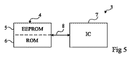
図5は、EEPROMに相当する部分5 (EEPROM)と、読出し専用メモリ、例えば図3と関連して既に説明したメモリに相当する部分6 (ROM)とを有するメモリ4 を備えた電子回路3 を概略的に示している。電子回路3 は、別の集積回路7(IC) を更に備えており、該集積回路7 は、メモリ4 の部分5 へのデータの書込み、及びメモリ4 の部分5 又は部分6 に記憶されたデータの読出しのために、接続部8 、例えばデータ交換バスによってメモリ4 に接続された例えばインターフェース回路である。
FIG. 5 shows an
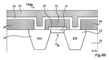
図6Aは、図2に示されたメモリセルのタイプのメモリセルCellB の側断面図である。図6Bは、図6Aの線A-A に沿った断面図であり、図6Cは、図6Aの線B-B に沿った断面図である。 FIG. 6A is a cross-sectional side view of a memory cell Cell B of the type of memory cell shown in FIG. 6B is a cross-sectional view taken along line AA in FIG. 6A, and FIG. 6C is a cross-sectional view taken along line BB in FIG. 6A.
セルCellB は、半導体基板10の活性領域に形成されており、半導体基板10は、典型的には単結晶シリコンから形成されており、絶縁領域12(STI 、図6B)によって横方向に画定されている。トランジスタTB及びメモリポイントTB' のゲート構造は半導体基板10上に形成されている。トランジスタTBのゲートは、第1の絶縁部分13、第1の導電性部分14、第2の絶縁部分15及び第2の導電性部分16の積層体から形成されている。また、トランジスタTBのゲートは、トランジスタTBの動作のために、従来のシングルゲートMOS トランジスタのゲートと同様であることが望ましい。このために、第1の導電性部分14及び第2の導電性部分16は、不図示の金属性のトラック及びバイアによって短絡されてもよい。
The cell Cell B is formed in the active region of the
メモリポイントTB' のゲートは、第1の絶縁部分20、第1の導電性部分21、第2の絶縁部分22及び第2の導電性部分23の積層体から形成されている。図6Bでは、半導体基板10上に延びてメモリセルCellBに属さない他の導電性部分24が示されている。第1の導電性部分21は、メモリポイントTB' の浮遊ゲートを形成している。第2の導電性部分23は、メモリポイントTB' の制御ゲートを形成している。第2の導電性部分23は、導電性ストリップに相当し、他のメモリポイントの制御ゲートを更に形成してもよい。第1の絶縁部分20は、浮遊ゲート21の絶縁体の非トンネル部分を形成する比較的厚い部分25と、トンネル酸化物領域を形成する比較的薄い部分26とを有する。比較的厚い部分25より薄い比較的薄い部分26は、絶縁領域12の上面で活性領域の全幅に亘って延びている。スペーサ27が、トランジスタTB及びメモリポイントTB' の両側に形成されている。
The gate of the memory point T B ′ is formed from a stacked body of the first insulating
変更されたEEPROMセルCellB では、第2の絶縁部分22は比較的厚い部分28と比較的薄い部分29とを有している。変更されていないEEPROMセルCellAは、第2の絶縁部分22が略一定の厚さを有している点を除いて、図6A乃至6Cに示された構造と同一の構造を有してもよい。
In the modified EEPROM cell Cell B , the second insulating
第1の導電性部分21及び第2の導電性部分23は、例えばポリシリコンから形成されており、第1の導電性部分21は約100nm の厚さを有しており、第2の導電性部分23は約200nm の厚さを有している。第1の絶縁部分20は、酸化物から形成されており、例えば酸化シリコン(SiO2)から形成されている。第2の絶縁部分22の比較的厚い部分28は、例えば全体の厚さが約180nm である酸化物−窒化物−酸化物積層体(「ONO 」積層体)を備えている。一例として、ONO 積層体では、酸化物は酸化シリコンであってもよく、窒化物は窒化シリコンであってもよい。第2の絶縁部分22の比較的薄い部分29は、例えば、数ナノメートル例えば2乃至3nmの厚さを有する酸化シリコン部分に相当する。一般的に、比較的厚い部分28は100nm より大きい厚さを有しており、比較的薄い部分29は5nm より小さい厚さを有している。
The first
トランジスタTB及びメモリポイントTB' の両側では、トランジスタTBのドレイン及びソースと、メモリポイントTB' のドレイン及びソースとの注入領域30が、半導体基板10に形成されている(トランジスタTBのソース領域及びメモリポイントTB' のドレイン領域が結合されている)。他の2つの注入領域31が、半導体基板10の表面に形成されて、メモリポイントTB' の絶縁部分25の下に部分的に延びている。
'In both sides of the drain and source of the transistor T B, the memory points T B' transistor T B and the memory point T B implanted
一例として、メモリポイントTB' は、断面B-B に、長辺L1が840nm であり短辺l1が640nm である略矩形状の断面を有している。薄い部分29は、例えば、メモリポイントTB' に関して中心部に設けられている。薄い部分29は、例えば断面B-B に、長辺L2が400nm であり短辺l2が320nm である略矩形状の断面を有している。
As an example, the memory point T B ′ has a substantially rectangular cross section having a long side L 1 of 840 nm and a short side l 1 of 640 nm in the cross section BB. The
薄い部分29は、EEPROMセルのメモリポイントTA' の2つのゲート間に通常設けられる厚い部分28より絶縁性が低く、薄い部分29の存在により、浮遊ゲート21に蓄えられた電荷の漏出が可能になる。薄い部分29の大きさは、電荷の排出が可能な限り速く行われるように選択されている。本出願人は、一例として既に述べられた薄い部分29の大きさについて、削除ステップ後の浮遊ゲート21に蓄えられた電荷の数が数ミリ秒以内に略90%減少していることを示している。
The
図7A乃至7Jは、図6Aに示されたセルCellB のような変更されたEEPROMセルを製造するための方法の連続的なステップで得られた構造の側断面図である。図8A乃至8Jは、図7A乃至7Jの(図7Aに示された)線C-C に沿った断面図である。 FIGS. 7A-7J are cross-sectional side views of structures obtained in successive steps of a method for manufacturing a modified EEPROM cell, such as cell Cell B shown in FIG. 6A. 8A-8J are cross-sectional views along line CC (shown in FIG. 7A) of FIGS. 7A-7J.
図7A及び8Aは、
P 型ドープ処理された単結晶シリコン基板80に、メモリセルの絶縁ウェル81(STI) を形成するステップ、
基板80に、図6Aに示された注入領域31に相当するN 型ドープ領域82を形成するステップ、及び、
選択トランジスタ及びメモリポイントの組立体を覆う酸化物層83を形成するステップの後に得られた構造を示している。一例として、酸化物層83は酸化シリコンから形成されてもよい。
7A and 8A are
Forming an insulating well 81 (STI) of a memory cell on a P-doped single
Forming an N-type doped
It shows the structure obtained after the step of forming an
図7B及び8Bは、メモリポイントのトンネル窓の位置で酸化物層83の一部(開口部85)を除去すべく酸化物層83をエッチングした後に得られた構造を示している。一例として、開口部85はウェットエッチングによって形成されてもよい。
FIGS. 7B and 8B show the structure obtained after etching the
図7C及び8Cは、図7B及び8Bに示された構造上に絶縁層を形成した後に得られた構造を示している。従って、この最後に形成された絶縁層及び下にある酸化物層83から形成された絶縁層86が、開口部85の位置に厚さがより薄い部分を有している。メモリポイントの浮遊ゲートの絶縁層及び選択トランジスタの第1の絶縁層は、このようにして形成される。
7C and 8C show the structure obtained after forming an insulating layer on the structure shown in FIGS. 7B and 8B. Therefore, the insulating
図7D及び8Dは、構造全体に第1のポリシリコン層87を形成した後に得られた構造を示している。
7D and 8D show the structure obtained after forming the
図7E及び8Eは、隣接したセルからEEPROMセルを分離する開口部88を形成すべく第1のポリシリコン層87をエッチングした後に得られた構造を示している。開口部88は、絶縁ウェル81(STI) 上に形成されている。
FIGS. 7E and 8E show the structure obtained after etching the
図7F及び8Fは、第1のポリシリコン層87及び開口部88の壁及び底に絶縁層89を形成した後に得られた構造を示している。一例として、絶縁層89は、例えば、第1の酸化シリコン層90、窒化シリコン層91及び第2の酸化シリコン層92から形成された酸化物−窒化物−酸化物(ONO) 積層体から形成されてもよい。
7F and 8F show the structure obtained after forming the insulating
図7G及び8Gは、ONO 積層体(90,91,92)に開口部94を形成し、開口部94の位置で第1のポリシリコン層87に絶縁層96を形成した後に得られた構造を示している。一例として、開口部94は、第2の酸化シリコン層92及び窒化シリコン層91をエッチングするためのドライエッチングと、ドライエッチング後の第1の酸化シリコン層90を除去するためのウェットエッチングとの2つの連続したエッチング動作によって得られてもよい。絶縁層96は、第1のポリシリコン層87の酸化によって得られてもよい。絶縁層96の部分は、図6Aに示されたメモリセルCellB の薄い部分29に相当する。
7G and 8G show the structure obtained after the
図7H及び8Hは、図7G及び8Gに示された構造上に第2のポリシリコン層98を形成した後に得られた構造を示している。
FIGS. 7H and 8H show the structure obtained after forming the
図7I及び8Iは、選択トランジスタ及びメモリポイントのゲートを画定し、選択トランジスタ及びメモリポイントのソース及びドレイン領域を形成した後に得られた構造を示している。このために、第2のポリシリコン層98、ONO 積層体(90,91,92)、第1のポリシリコン層87及び絶縁層86の組立体がエッチングされて開口部100 が形成される。その後、N 型ドープ領域102 が開口部100 の位置で基板80に形成されて、選択トランジスタ及びメモリポイントのソース及びドレインが形成される。
FIGS. 7I and 8I show the structure obtained after defining the gates of the select transistors and memory points and forming the source and drain regions of the select transistors and memory points. For this purpose, the assembly of the
図7J及び8Jは、選択トランジスタ及びメモリポイントの上部及び両側に薄い絶縁層104 を形成した後に得られた構造を示している。絶縁層104 は熱酸化によって得られてもよい。その後、スペーサが、選択トランジスタ及びメモリポイントの両側に任意の通常の方法によって形成され得る。
7J and 8J show the structure obtained after forming a thin
メモリセルを形成するための上記の方法により、変更されたEEPROMセルと変更されていないEEPROMセルとを同時に形成することが可能になる。実際には、図7G及び8Gに関連して既に説明されたステップで、変更されたEEPROMセルのための薄い部分96を形成するだけで十分であり、変更されていないEEPROMセルのために絶縁層89をエッチングする必要がない。従って、既に説明した方法は、EEPROMに相当する第1の部分と、読出し専用メモリに相当する第2の部分とを備えたメモリを形成するために実施され得る。
The above method for forming a memory cell allows a modified EEPROM cell and an unmodified EEPROM cell to be formed simultaneously. In practice, it is sufficient to form the
更に、通常のEEPROMセルを形成する方法と比較すると、本方法は、追加のステップを必要としないという利点を有する。実際には通常、EEPROMセルが形成されるとき、低電圧シングルゲートMOS トランジスタが同一の基板に更に形成される。低電圧トランジスタは、第1のポリシリコン層87が除去される位置で基板の領域上及び領域中に形成される。低電圧トランジスタのゲート絶縁体及びゲートは、絶縁層96及び第2のポリシリコン層98によって夫々形成される。従って、図6A乃至6Cに示された構造を得るために、開口部94の位置で構造に開口部を追加することにより、低電圧トランジスタの位置でONO 積層体を除去するために通常使用されるマスクを変更するだけで十分である。更に、図6A乃至6Cに示された構造は、プログラミング、読出し及び書込みの点で他のセルと完全に互換性を有するという利点を有する。
Furthermore, compared to the method of forming a normal EEPROM cell, the method has the advantage that no additional steps are required. In practice, when an EEPROM cell is typically formed, a low voltage single gate MOS transistor is further formed on the same substrate. The low voltage transistor is formed on and in the region of the substrate at the location where the
好ましくは、比較的薄い部分96が比較的厚い部分89に完全に囲まれるように薄い部分96の大きさ及び位置が選択されている。これにより、図7I及び8Iと関連して既に説明されたステップで、全てのメモリセルのために積層状の厚い部分89のみをエッチングすることが可能になる。これによって、このステップのための従来のEEPROM製造工程を変更しないことが可能になる。実際には、変更されていないEEPROMセルのために絶縁性の厚い部分89をエッチングする必要がある場合、及び変更されたEEPROMセルのために絶縁性の薄い部分96をエッチングする必要がある場合、絶縁性の厚い部分89及び絶縁性の薄い部分96の厚さ及び構造が異なると仮定すると、2回の別個のエッチングステップを設ける必要がある。
Preferably, the size and position of the
従来のROM と比較すると、本実施形態に係るメモリと関連した相互接続トラックは、プログラミングのために変更されない。従って、本実施形態に係るメモリのプログラミングは、メタライゼーションを上から見ても、このメタライゼーションに使用されるマスクを分析しても、又はこのマスクを再構築すべく連続的な断面を検査しても(ディレイアリング)明らかにならない。 Compared to a conventional ROM, the interconnect track associated with the memory according to this embodiment is not changed for programming. Therefore, the programming of the memory according to this embodiment can be performed by looking at the metallization from above, analyzing the mask used for this metallization, or inspecting a continuous cross-section to reconstruct this mask. But (delaying) does not become clear.
更に、例えば、絶縁トレンチ(STI) の位置に開口部94を設けることにより、開口部94を形成すべく使用されるマスクの可能な分析を防ぐために寄生パターンを追加してもよい。
Further, a parasitic pattern may be added to prevent possible analysis of the mask used to form the
本発明の特定の実施形態が説明されている。様々な変更及び調整が当業者に想起される。特に、本発明はメモリポイント及び選択トランジスタを備えたメモリセルに関して説明されているが、本発明は、浮遊ゲートを有するデュアルゲートトランジスタを備えた任意のタイプのEEPROMセルに関して実施され得ることは明らかである。これは、図1に示されたセルと比較すると、メモリセルがメモリポイントTA' のみを備えてもよいフラッシュメモリの場合である。 Particular embodiments of the present invention have been described. Various changes and adjustments will occur to those skilled in the art. In particular, although the present invention has been described with respect to a memory cell with a memory point and a select transistor, it should be apparent that the present invention can be implemented with any type of EEPROM cell with a dual gate transistor having a floating gate. is there. This is the case for a flash memory in which the memory cell may comprise only the memory point T A ′ compared to the cell shown in FIG.
Claims (9)
前記第2のメモリセルの蓄積トランジスタの絶縁層は、前記第1のメモリセルの蓄積トランジスタの絶縁層より絶縁性が低い少なくとも1つの部分を有しており、
前記第1のメモリセルの蓄積トランジスタの絶縁層は、100nm より大きい第1の厚さを有しており、前記第2のメモリセルの蓄積トランジスタの絶縁層の前記部分は、5nmより小さい第2の厚さを有することを特徴とするメモリ。 At least first and includes a second Memorise le, the first and second memory cells,蓄Sekito Rungis data and a provided between the two gates and the two gate insulating layer the a non-volatile memory that contains respectively,
The insulating layer of the storage transistor capacitor of the second Memorise Le has to have at least one part component is less insulating than the insulating layer of the storage transistor capacitor of the first Memorise Le,
The insulating layer of the storage transistor of the first memory cell has a first thickness greater than 100 nm, and the portion of the insulating layer of the storage transistor of the second memory cell has a second thickness of less than 5 nm. A memory having a thickness of
前記第2のメモリセルの蓄積トランジスタの絶縁層の第2の厚さを有する前記部分は、第3の酸化シリコン層から形成されていることを特徴とする請求項1又は2に記載のメモリ。 Insulating layer having a storage transistor first thickness data of said first Memorise Le, the first silicon oxide layer, is formed of a laminate of the second silicon oxide layer a silicon nitride So及 Beauty,
Wherein the unit component having a second thickness of the second Memorise Le insulating layer of the storage transistor data of, according to claim 1 or 2, characterized in that it is formed a third silicon oxide layer of either et al Memory.
前記第2のメモリセルの蓄積トランジスタの第2の絶縁層は、前記少なくとも1つの部分を有しており、
前記メモリは、半導体材料から形成された基板を更に備えており、
前記第1の絶縁層は、前記基板を覆い、第2の絶縁部分より薄い第1の絶縁部分を有することを特徴とする請求項1に記載のメモリ。 It said first and second Memorise Le accumulation transistor motor, the first insulating layer, the first gate comprises a second insulating So及 beauty laminate of the second gate,
The second insulating layer of the storage transistor capacitor of the second Memorise le has the at least one part component,
The memory further comprises a board formed from a semiconductor material,
The first insulating layer covers the substrate, memory of claim 1, characterized in that it comprises a second insulator portion component first insulating portion partial thin Ri by.
前記第2のメモリセルの蓄積トランジスタの絶縁層に、前記第1のメモリセルの蓄積トランジスタの絶縁層より絶縁性が低い少なくとも1つの部分を形成するステップを有し、
前記第1のメモリセルの蓄積トランジスタの絶縁層は、100nm より大きい第1の厚さを有しており、前記第2のメモリセルの蓄積トランジスタの絶縁層の前記部分は、5nmより小さい第2の厚さを有することを特徴とする方法。 Comprises at least first and second Memorise le, the first and second memory cells, the storage preparative Rungis data that have a and provided between the two gates and the two gate insulating layer a method for forming a memory, each of which has,
The insulating layer of the storage transistor capacitor of the second Memorise Le, have a step of forming at least one part component is less insulating than the insulating layer of the storage transistor capacitor of the first Memorise Le,
The insulating layer of the storage transistor of the first memory cell has a first thickness greater than 100 nm, and the portion of the insulating layer of the storage transistor of the second memory cell has a second thickness of less than 5 nm. Having a thickness of :
前記第1及び第2のメモリセル毎に、前記第1のゲートに第1の絶縁層を形成するステップと、
前記第2のメモリセルのみに、前記第1の絶縁層に開口部を形成するステップと、
前記開口部に、前記第1の絶縁層より絶縁性が低い第2の絶縁層を形成するステップと
を連続的に行うことを特徴とする請求項6に記載の方法。 For each of the first and second Memorise Le, even after the step of forming a first gate of the storage transistor data, before the step of forming a second gate of the storage transistor motor,
Forming a first insulating layer on the first gate for each of the first and second memory cells;
Forming an opening the second Memorise Le mini, the first insulating layer,
Wherein the opening, The method of claim 6, characterized in that the step of forming a second insulating layer is less insulating than the first insulating layer successively.
前記第2の絶縁層は第3の酸化シリコン層から形成されていることを特徴とする請求項7に記載の方法。 The first insulating layer, a first silicon oxide layer, is formed of a laminate of the second silicon oxide layer a silicon nitride So及 Beauty,
The method of claim 7, wherein the second insulating layer is formed from a third silicon oxide layer.
前記第1及び第2のメモリセル毎に、蓄積トランジスタの2つのゲートの内の第1のゲートに電荷を注入して、前記第1のメモリセルでは第1のゲートに電荷を蓄え、前記第2のメモリセルでは2つのゲートの内の第1のゲートから他方のゲートに電荷を排出するステップと、
前記第1及び第2のメモリセル毎に前記第1のゲートに蓄えられた電荷を表すデータを測定するステップと
を連続的に行うことを特徴とする方法。 Be any memory or these reading method of claims 1 to 4,
For each of the first and second Memorise Le, by injecting electric charges into the first gate of the two gates of the storage transistors data, wherein in the first Memorise Le accumulated charge to the first gate a step wherein in the second Memorise Le discharging the charge from the first gate of the two gates to the other of the gate,
Continuously measuring the data representing the charge stored in the first gate for each of the first and second memory cells.
Applications Claiming Priority (3)
| Application Number | Priority Date | Filing Date | Title |
|---|---|---|---|
| FR0853069A FR2931289A1 (en) | 2008-05-13 | 2008-05-13 | MEMORY WITH EEPROM TYPE STRUCTURE AND READ ONLY |
| FR0853069 | 2008-05-13 | ||
| PCT/FR2009/050868 WO2009147347A1 (en) | 2008-05-13 | 2009-05-12 | Read-only memory with eeprom structure |
Publications (2)
| Publication Number | Publication Date |
|---|---|
| JP2011523205A JP2011523205A (en) | 2011-08-04 |
| JP5497744B2 true JP5497744B2 (en) | 2014-05-21 |
Family
ID=39749732
Family Applications (1)
| Application Number | Title | Priority Date | Filing Date |
|---|---|---|---|
| JP2011508982A Active JP5497744B2 (en) | 2008-05-13 | 2009-05-12 | Read only memory having EEPROM structure |
Country Status (7)
| Country | Link |
|---|---|
| US (1) | US8759898B2 (en) |
| EP (1) | EP2286450B1 (en) |
| JP (1) | JP5497744B2 (en) |
| CN (1) | CN102027588B (en) |
| AT (1) | ATE529892T1 (en) |
| FR (1) | FR2931289A1 (en) |
| WO (1) | WO2009147347A1 (en) |
Families Citing this family (5)
| Publication number | Priority date | Publication date | Assignee | Title |
|---|---|---|---|---|
| US20120225271A1 (en) * | 2011-02-17 | 2012-09-06 | Alcoa Inc. | 2xxx series aluminum lithium alloys |
| US9287879B2 (en) * | 2011-06-07 | 2016-03-15 | Verisiti, Inc. | Semiconductor device having features to prevent reverse engineering |
| FR2978867B1 (en) | 2011-08-01 | 2014-03-21 | St Microelectronics Rousset | ADJUSTABLE RESISTANCE |
| US9171856B2 (en) * | 2013-10-01 | 2015-10-27 | Ememory Technology Inc. | Bias generator for flash memory and control method thereof |
| CN105810252B (en) * | 2014-12-31 | 2018-10-16 | 展讯通信(上海)有限公司 | A kind of storage unit, storage unit defect detection circuit and memory |
Family Cites Families (20)
| Publication number | Priority date | Publication date | Assignee | Title |
|---|---|---|---|---|
| JPS57130473A (en) * | 1981-02-05 | 1982-08-12 | Seiko Epson Corp | Mos type semiconductor memory storage |
| JPS6367783A (en) * | 1986-09-09 | 1988-03-26 | Mitsubishi Electric Corp | Semiconductor storage device |
| FR2623651B1 (en) * | 1987-11-20 | 1992-11-27 | Sgs Thomson Microelectronics | MEMORY PLAN AND METHOD AND PROTOTYPE FOR DEFINING AN ELECTRONIC INTEGRATED CIRCUIT COMPRISING SUCH A MEMORY PLAN |
| DE3743224A1 (en) | 1987-12-19 | 1989-06-29 | Merck Patent Gmbh | METHOD AND REAGENT FOR DETERMINING PERSAURERS |
| JP2807256B2 (en) * | 1989-03-17 | 1998-10-08 | 株式会社東芝 | Non-volatile semiconductor memory |
| KR920013709A (en) * | 1990-12-21 | 1992-07-29 | 김광호 | Nonvolatile semiconductor memory device and manufacturing method thereof |
| JP3222705B2 (en) * | 1993-11-30 | 2001-10-29 | 東芝マイクロエレクトロニクス株式会社 | Nonvolatile semiconductor memory device and method of manufacturing the same |
| JPH0878544A (en) * | 1994-08-31 | 1996-03-22 | Toshiba Corp | Nonvolatile semiconductor memory |
| KR100215840B1 (en) * | 1996-02-28 | 1999-08-16 | 구본준 | Structure of a semiconductor and manufacturing method thereof |
| JP3123924B2 (en) * | 1996-06-06 | 2001-01-15 | 三洋電機株式会社 | Non-volatile semiconductor memory |
| US5792697A (en) * | 1997-01-07 | 1998-08-11 | United Microelectronics Corporation | Method for fabricating a multi-stage ROM |
| DE69734509D1 (en) * | 1997-07-08 | 2005-12-08 | St Microelectronics Srl | Electrically programmable, non-volatile semiconductor memory cell matrix with ROM memory cells |
| JP2002074998A (en) * | 2000-08-23 | 2002-03-15 | Matsushita Electric Ind Co Ltd | Evaluation device of non-volatile semiconductor memory and its evaluating method, and non-volatile semiconductor memory and its manufacturing method |
| AU2001293248A1 (en) * | 2000-10-03 | 2002-04-15 | Abraham R. Zingher | Biometric system and method for detecting duress transactions |
| KR100423075B1 (en) * | 2001-12-19 | 2004-03-16 | 삼성전자주식회사 | Semiconductor Device And Method Of Fabricating The Same |
| TWI257150B (en) * | 2005-02-03 | 2006-06-21 | Powerchip Semiconductor Corp | Non-volatile memory and fabricating method and operating method thereof |
| JP4892199B2 (en) | 2005-06-06 | 2012-03-07 | ルネサスエレクトロニクス株式会社 | Method for manufacturing nonvolatile semiconductor memory device |
| KR100676204B1 (en) * | 2005-08-25 | 2007-01-30 | 삼성전자주식회사 | Memory cell transistor for eeprom |
| KR100725171B1 (en) * | 2006-01-06 | 2007-06-04 | 삼성전자주식회사 | Semiconductor device with mask read-only-memory(rom) device and method of fabricating the same |
| JP4921848B2 (en) * | 2006-05-09 | 2012-04-25 | 株式会社東芝 | Semiconductor device and manufacturing method thereof |
-
2008
- 2008-05-13 FR FR0853069A patent/FR2931289A1/en not_active Withdrawn
-
2009
- 2009-05-12 JP JP2011508982A patent/JP5497744B2/en active Active
- 2009-05-12 US US12/990,682 patent/US8759898B2/en active Active
- 2009-05-12 EP EP09757723A patent/EP2286450B1/en active Active
- 2009-05-12 CN CN2009801172498A patent/CN102027588B/en active Active
- 2009-05-12 WO PCT/FR2009/050868 patent/WO2009147347A1/en active Application Filing
- 2009-05-12 AT AT09757723T patent/ATE529892T1/en not_active IP Right Cessation
Also Published As
| Publication number | Publication date |
|---|---|
| EP2286450A1 (en) | 2011-02-23 |
| ATE529892T1 (en) | 2011-11-15 |
| CN102027588A (en) | 2011-04-20 |
| US20110108902A1 (en) | 2011-05-12 |
| FR2931289A1 (en) | 2009-11-20 |
| US8759898B2 (en) | 2014-06-24 |
| EP2286450B1 (en) | 2011-10-19 |
| WO2009147347A1 (en) | 2009-12-10 |
| CN102027588B (en) | 2013-12-04 |
| JP2011523205A (en) | 2011-08-04 |
Similar Documents
| Publication | Publication Date | Title |
|---|---|---|
| KR101124159B1 (en) | A semiconductor device and a method of manufacturing the same | |
| US6337250B2 (en) | Semiconductor device containing MOS elements and method of fabricating the same | |
| JP4818061B2 (en) | Nonvolatile semiconductor memory | |
| JPH11186419A (en) | Non-volatile semiconductor storage device | |
| KR100922460B1 (en) | Nonvolatile semiconductor memory | |
| US7256443B2 (en) | Semiconductor memory and method of manufacturing the same | |
| JP5497744B2 (en) | Read only memory having EEPROM structure | |
| KR100364040B1 (en) | A semiconductor memory device and a method of making thereof | |
| US7439577B2 (en) | Semiconductor memory and method for manufacturing the same | |
| JP2007250854A (en) | Semiconductor memory device and its manufacturing method | |
| JP5039368B2 (en) | Semiconductor memory device, manufacturing method thereof and driving method thereof | |
| US6268247B1 (en) | Memory cell of the EEPROM type having its threshold set by implantation, and fabrication method | |
| JP2007157927A (en) | Non-volatile semiconductor memory device and method of manufacturing same | |
| US7611946B2 (en) | Method of fabricating a non-volatile memory device | |
| EP0432792A2 (en) | Nonvolatile semiconductor memory device and method of manufacturing the same | |
| US20060234452A1 (en) | Non-volatile memory and fabricating method thereof | |
| JP2007180150A (en) | Non-volatile semiconductor storage device and manufacturing method thereof | |
| JP2006210700A (en) | Nonvolatile semiconductor memory device and its manufacturing method | |
| US20020132424A1 (en) | Semiconductor devices having a non-volatile memory transistor and methods for manufacturing the same | |
| JP2007067043A (en) | Semiconductor device and its manufacturing method | |
| US7705393B2 (en) | Nonvolatile semiconductor storage device having silicide in control gate electrode | |
| US7361553B2 (en) | Semiconductor device manufacturing method | |
| JP4016679B2 (en) | Semiconductor device and manufacturing method of semiconductor device | |
| US6921964B2 (en) | Semiconductor device having a non-volatile memory transistor formed on a semiconductor | |
| US11101000B2 (en) | Semiconductor device and method for operating the same |
Legal Events
| Date | Code | Title | Description |
|---|---|---|---|
| A621 | Written request for application examination |
Free format text: JAPANESE INTERMEDIATE CODE: A621 Effective date: 20120507 |
|
| A131 | Notification of reasons for refusal |
Free format text: JAPANESE INTERMEDIATE CODE: A131 Effective date: 20131015 |
|
| A977 | Report on retrieval |
Free format text: JAPANESE INTERMEDIATE CODE: A971007 Effective date: 20131017 |
|
| A521 | Request for written amendment filed |
Free format text: JAPANESE INTERMEDIATE CODE: A523 Effective date: 20140109 |
|
| TRDD | Decision of grant or rejection written | ||
| A01 | Written decision to grant a patent or to grant a registration (utility model) |
Free format text: JAPANESE INTERMEDIATE CODE: A01 Effective date: 20140212 |
|
| A61 | First payment of annual fees (during grant procedure) |
Free format text: JAPANESE INTERMEDIATE CODE: A61 Effective date: 20140306 |
|
| R150 | Certificate of patent or registration of utility model |
Ref document number: 5497744 Country of ref document: JP Free format text: JAPANESE INTERMEDIATE CODE: R150 |
|
| R250 | Receipt of annual fees |
Free format text: JAPANESE INTERMEDIATE CODE: R250 |
|
| R250 | Receipt of annual fees |
Free format text: JAPANESE INTERMEDIATE CODE: R250 |
|
| R250 | Receipt of annual fees |
Free format text: JAPANESE INTERMEDIATE CODE: R250 |
|
| R250 | Receipt of annual fees |
Free format text: JAPANESE INTERMEDIATE CODE: R250 |
|
| R250 | Receipt of annual fees |
Free format text: JAPANESE INTERMEDIATE CODE: R250 |
|
| R250 | Receipt of annual fees |
Free format text: JAPANESE INTERMEDIATE CODE: R250 |
|
| R250 | Receipt of annual fees |
Free format text: JAPANESE INTERMEDIATE CODE: R250 |
|
| R250 | Receipt of annual fees |
Free format text: JAPANESE INTERMEDIATE CODE: R250 |