JP5496673B2 - Structured thermal transfer donor - Google Patents
Structured thermal transfer donor Download PDFInfo
- Publication number
- JP5496673B2 JP5496673B2 JP2009533458A JP2009533458A JP5496673B2 JP 5496673 B2 JP5496673 B2 JP 5496673B2 JP 2009533458 A JP2009533458 A JP 2009533458A JP 2009533458 A JP2009533458 A JP 2009533458A JP 5496673 B2 JP5496673 B2 JP 5496673B2
- Authority
- JP
- Japan
- Prior art keywords
- transfer layer
- transfer
- layer
- shape
- receptor
- Prior art date
- Legal status (The legal status is an assumption and is not a legal conclusion. Google has not performed a legal analysis and makes no representation as to the accuracy of the status listed.)
- Active
Links
- 239000000758 substrate Substances 0.000 claims description 40
- 238000000034 method Methods 0.000 claims description 32
- 238000006243 chemical reaction Methods 0.000 claims description 14
- 239000011159 matrix material Substances 0.000 claims description 5
- 238000004519 manufacturing process Methods 0.000 claims description 3
- 239000010410 layer Substances 0.000 description 212
- 239000010408 film Substances 0.000 description 79
- 239000000543 intermediate Substances 0.000 description 36
- 238000003384 imaging method Methods 0.000 description 29
- 239000000463 material Substances 0.000 description 24
- 229910052751 metal Inorganic materials 0.000 description 14
- 239000002184 metal Substances 0.000 description 14
- 230000003287 optical effect Effects 0.000 description 9
- 230000005855 radiation Effects 0.000 description 8
- 239000000975 dye Substances 0.000 description 6
- 150000002739 metals Chemical class 0.000 description 6
- 239000006100 radiation absorber Substances 0.000 description 6
- 239000004065 semiconductor Substances 0.000 description 6
- 238000000576 coating method Methods 0.000 description 5
- -1 surfaces Substances 0.000 description 5
- 239000011248 coating agent Substances 0.000 description 4
- 239000011888 foil Substances 0.000 description 4
- 239000011521 glass Substances 0.000 description 4
- 230000008569 process Effects 0.000 description 4
- 239000000853 adhesive Substances 0.000 description 3
- 230000001070 adhesive effect Effects 0.000 description 3
- 238000004049 embossing Methods 0.000 description 3
- 238000010438 heat treatment Methods 0.000 description 3
- AMGQUBHHOARCQH-UHFFFAOYSA-N indium;oxotin Chemical compound [In].[Sn]=O AMGQUBHHOARCQH-UHFFFAOYSA-N 0.000 description 3
- 229910010272 inorganic material Inorganic materials 0.000 description 3
- 239000011147 inorganic material Substances 0.000 description 3
- 239000011229 interlayer Substances 0.000 description 3
- 238000000608 laser ablation Methods 0.000 description 3
- 229910044991 metal oxide Inorganic materials 0.000 description 3
- 150000004706 metal oxides Chemical class 0.000 description 3
- 238000000059 patterning Methods 0.000 description 3
- 229920000139 polyethylene terephthalate Polymers 0.000 description 3
- 239000005020 polyethylene terephthalate Substances 0.000 description 3
- 229920000642 polymer Polymers 0.000 description 3
- 229920001187 thermosetting polymer Polymers 0.000 description 3
- VYPSYNLAJGMNEJ-UHFFFAOYSA-N Silicium dioxide Chemical compound O=[Si]=O VYPSYNLAJGMNEJ-UHFFFAOYSA-N 0.000 description 2
- GWEVSGVZZGPLCZ-UHFFFAOYSA-N Titan oxide Chemical compound O=[Ti]=O GWEVSGVZZGPLCZ-UHFFFAOYSA-N 0.000 description 2
- 238000000151 deposition Methods 0.000 description 2
- 238000005516 engineering process Methods 0.000 description 2
- 238000005530 etching Methods 0.000 description 2
- 230000005669 field effect Effects 0.000 description 2
- 239000002086 nanomaterial Substances 0.000 description 2
- 239000011368 organic material Substances 0.000 description 2
- 229920006255 plastic film Polymers 0.000 description 2
- 239000002985 plastic film Substances 0.000 description 2
- 229920006254 polymer film Polymers 0.000 description 2
- 239000000126 substance Substances 0.000 description 2
- 239000004593 Epoxy Substances 0.000 description 1
- 239000004743 Polypropylene Substances 0.000 description 1
- 229910052581 Si3N4 Inorganic materials 0.000 description 1
- 238000002679 ablation Methods 0.000 description 1
- 239000011358 absorbing material Substances 0.000 description 1
- 230000009102 absorption Effects 0.000 description 1
- 238000010521 absorption reaction Methods 0.000 description 1
- 230000006978 adaptation Effects 0.000 description 1
- 239000000654 additive Substances 0.000 description 1
- 229910052782 aluminium Inorganic materials 0.000 description 1
- XAGFODPZIPBFFR-UHFFFAOYSA-N aluminium Chemical compound [Al] XAGFODPZIPBFFR-UHFFFAOYSA-N 0.000 description 1
- 238000004458 analytical method Methods 0.000 description 1
- 239000003990 capacitor Substances 0.000 description 1
- 239000006229 carbon black Substances 0.000 description 1
- 239000000919 ceramic Substances 0.000 description 1
- 239000002131 composite material Substances 0.000 description 1
- 239000004020 conductor Substances 0.000 description 1
- 238000010276 construction Methods 0.000 description 1
- 238000011109 contamination Methods 0.000 description 1
- 230000008878 coupling Effects 0.000 description 1
- 238000010168 coupling process Methods 0.000 description 1
- 238000005859 coupling reaction Methods 0.000 description 1
- 238000005520 cutting process Methods 0.000 description 1
- 230000032798 delamination Effects 0.000 description 1
- 239000000412 dendrimer Substances 0.000 description 1
- 229920000736 dendritic polymer Polymers 0.000 description 1
- 229910003460 diamond Inorganic materials 0.000 description 1
- 239000010432 diamond Substances 0.000 description 1
- 238000005553 drilling Methods 0.000 description 1
- 230000000694 effects Effects 0.000 description 1
- 125000003700 epoxy group Chemical group 0.000 description 1
- 239000000835 fiber Substances 0.000 description 1
- 239000012530 fluid Substances 0.000 description 1
- 239000007850 fluorescent dye Substances 0.000 description 1
- 238000000227 grinding Methods 0.000 description 1
- BHEPBYXIRTUNPN-UHFFFAOYSA-N hydridophosphorus(.) (triplet) Chemical compound [PH] BHEPBYXIRTUNPN-UHFFFAOYSA-N 0.000 description 1
- 229910052809 inorganic oxide Inorganic materials 0.000 description 1
- 239000012212 insulator Substances 0.000 description 1
- 230000001788 irregular Effects 0.000 description 1
- 239000004973 liquid crystal related substance Substances 0.000 description 1
- 238000003754 machining Methods 0.000 description 1
- 150000002736 metal compounds Chemical class 0.000 description 1
- 239000007769 metal material Substances 0.000 description 1
- 229910052976 metal sulfide Inorganic materials 0.000 description 1
- 238000003801 milling Methods 0.000 description 1
- 238000012986 modification Methods 0.000 description 1
- 230000004048 modification Effects 0.000 description 1
- 125000002524 organometallic group Chemical group 0.000 description 1
- 238000000206 photolithography Methods 0.000 description 1
- 239000000049 pigment Substances 0.000 description 1
- 239000004033 plastic Substances 0.000 description 1
- 229920003023 plastic Polymers 0.000 description 1
- 239000004014 plasticizer Substances 0.000 description 1
- 229920000058 polyacrylate Polymers 0.000 description 1
- 229920000647 polyepoxide Polymers 0.000 description 1
- 229920000728 polyester Polymers 0.000 description 1
- 229920006267 polyester film Polymers 0.000 description 1
- 239000011112 polyethylene naphthalate Substances 0.000 description 1
- 229920000193 polymethacrylate Polymers 0.000 description 1
- 229920001155 polypropylene Polymers 0.000 description 1
- 229920002635 polyurethane Polymers 0.000 description 1
- 239000004814 polyurethane Substances 0.000 description 1
- 239000002243 precursor Substances 0.000 description 1
- 229920005989 resin Polymers 0.000 description 1
- 239000011347 resin Substances 0.000 description 1
- 230000000717 retained effect Effects 0.000 description 1
- 238000005389 semiconductor device fabrication Methods 0.000 description 1
- 238000000926 separation method Methods 0.000 description 1
- 229910052710 silicon Inorganic materials 0.000 description 1
- 239000010703 silicon Substances 0.000 description 1
- 239000000377 silicon dioxide Substances 0.000 description 1
- HQVNEWCFYHHQES-UHFFFAOYSA-N silicon nitride Chemical compound N12[Si]34N5[Si]62N3[Si]51N64 HQVNEWCFYHHQES-UHFFFAOYSA-N 0.000 description 1
- 239000002356 single layer Substances 0.000 description 1
- 238000005245 sintering Methods 0.000 description 1
- 150000003384 small molecules Chemical class 0.000 description 1
- 239000007787 solid Substances 0.000 description 1
- 238000001228 spectrum Methods 0.000 description 1
- 239000004094 surface-active agent Substances 0.000 description 1
- 229920001169 thermoplastic Polymers 0.000 description 1
- 239000012815 thermoplastic material Substances 0.000 description 1
- 239000004416 thermosoftening plastic Substances 0.000 description 1
- 239000010409 thin film Substances 0.000 description 1
- 239000002699 waste material Substances 0.000 description 1
- 238000009763 wire-cut EDM Methods 0.000 description 1
- 229910052724 xenon Inorganic materials 0.000 description 1
- FHNFHKCVQCLJFQ-UHFFFAOYSA-N xenon atom Chemical compound [Xe] FHNFHKCVQCLJFQ-UHFFFAOYSA-N 0.000 description 1
Images


Classifications
-
- B—PERFORMING OPERATIONS; TRANSPORTING
- B41—PRINTING; LINING MACHINES; TYPEWRITERS; STAMPS
- B41M—PRINTING, DUPLICATING, MARKING, OR COPYING PROCESSES; COLOUR PRINTING
- B41M5/00—Duplicating or marking methods; Sheet materials for use therein
- B41M5/26—Thermography ; Marking by high energetic means, e.g. laser otherwise than by burning, and characterised by the material used
- B41M5/40—Thermography ; Marking by high energetic means, e.g. laser otherwise than by burning, and characterised by the material used characterised by the base backcoat, intermediate, or covering layers, e.g. for thermal transfer dye-donor or dye-receiver sheets; Heat, radiation filtering or absorbing means or layers; combined with other image registration layers or compositions; Special originals for reproduction by thermography
- B41M5/42—Intermediate, backcoat, or covering layers
-
- H—ELECTRICITY
- H01—ELECTRIC ELEMENTS
- H01L—SEMICONDUCTOR DEVICES NOT COVERED BY CLASS H10
- H01L29/00—Semiconductor devices adapted for rectifying, amplifying, oscillating or switching, or capacitors or resistors with at least one potential-jump barrier or surface barrier, e.g. PN junction depletion layer or carrier concentration layer; Details of semiconductor bodies or of electrodes thereof ; Multistep manufacturing processes therefor
- H01L29/02—Semiconductor bodies ; Multistep manufacturing processes therefor
- H01L29/06—Semiconductor bodies ; Multistep manufacturing processes therefor characterised by their shape; characterised by the shapes, relative sizes, or dispositions of the semiconductor regions ; characterised by the concentration or distribution of impurities within semiconductor regions
- H01L29/0657—Semiconductor bodies ; Multistep manufacturing processes therefor characterised by their shape; characterised by the shapes, relative sizes, or dispositions of the semiconductor regions ; characterised by the concentration or distribution of impurities within semiconductor regions characterised by the shape of the body
- H01L29/0665—Semiconductor bodies ; Multistep manufacturing processes therefor characterised by their shape; characterised by the shapes, relative sizes, or dispositions of the semiconductor regions ; characterised by the concentration or distribution of impurities within semiconductor regions characterised by the shape of the body the shape of the body defining a nanostructure
-
- H—ELECTRICITY
- H10—SEMICONDUCTOR DEVICES; ELECTRIC SOLID-STATE DEVICES NOT OTHERWISE PROVIDED FOR
- H10K—ORGANIC ELECTRIC SOLID-STATE DEVICES
- H10K71/00—Manufacture or treatment specially adapted for the organic devices covered by this subclass
- H10K71/10—Deposition of organic active material
- H10K71/18—Deposition of organic active material using non-liquid printing techniques, e.g. thermal transfer printing from a donor sheet
-
- B—PERFORMING OPERATIONS; TRANSPORTING
- B41—PRINTING; LINING MACHINES; TYPEWRITERS; STAMPS
- B41M—PRINTING, DUPLICATING, MARKING, OR COPYING PROCESSES; COLOUR PRINTING
- B41M2205/00—Printing methods or features related to printing methods; Location or type of the layers
- B41M2205/02—Dye diffusion thermal transfer printing (D2T2)
-
- B—PERFORMING OPERATIONS; TRANSPORTING
- B41—PRINTING; LINING MACHINES; TYPEWRITERS; STAMPS
- B41M—PRINTING, DUPLICATING, MARKING, OR COPYING PROCESSES; COLOUR PRINTING
- B41M2205/00—Printing methods or features related to printing methods; Location or type of the layers
- B41M2205/38—Intermediate layers; Layers between substrate and imaging layer
-
- Y—GENERAL TAGGING OF NEW TECHNOLOGICAL DEVELOPMENTS; GENERAL TAGGING OF CROSS-SECTIONAL TECHNOLOGIES SPANNING OVER SEVERAL SECTIONS OF THE IPC; TECHNICAL SUBJECTS COVERED BY FORMER USPC CROSS-REFERENCE ART COLLECTIONS [XRACs] AND DIGESTS
- Y02—TECHNOLOGIES OR APPLICATIONS FOR MITIGATION OR ADAPTATION AGAINST CLIMATE CHANGE
- Y02E—REDUCTION OF GREENHOUSE GAS [GHG] EMISSIONS, RELATED TO ENERGY GENERATION, TRANSMISSION OR DISTRIBUTION
- Y02E10/00—Energy generation through renewable energy sources
- Y02E10/50—Photovoltaic [PV] energy
- Y02E10/549—Organic PV cells
-
- Y—GENERAL TAGGING OF NEW TECHNOLOGICAL DEVELOPMENTS; GENERAL TAGGING OF CROSS-SECTIONAL TECHNOLOGIES SPANNING OVER SEVERAL SECTIONS OF THE IPC; TECHNICAL SUBJECTS COVERED BY FORMER USPC CROSS-REFERENCE ART COLLECTIONS [XRACs] AND DIGESTS
- Y02—TECHNOLOGIES OR APPLICATIONS FOR MITIGATION OR ADAPTATION AGAINST CLIMATE CHANGE
- Y02P—CLIMATE CHANGE MITIGATION TECHNOLOGIES IN THE PRODUCTION OR PROCESSING OF GOODS
- Y02P70/00—Climate change mitigation technologies in the production process for final industrial or consumer products
- Y02P70/50—Manufacturing or production processes characterised by the final manufactured product
Description
本発明は、ミクロ構造化又はナノ構造化熱転写ドナーに関する。更に、本発明は、装置を作製するためにミクロ構造化又はナノ構造化熱転写ドナーを製作及び使用するための方法に関する。 The present invention relates to microstructured or nanostructured thermal transfer donors. Furthermore, the present invention relates to a method for making and using a microstructured or nanostructured thermal transfer donor to make a device.
産業及び消費者用途、特に電子装置に使用される多数の物品及び装置の寸法を減少する一般的な傾向が存在する。更に、様々な物品及び装置がミクロ構造化表面を利用する。これらの物品及び装置は、多くの場合、ミクロ構造化又はナノ構造化表面、層、若しくはコンポーネントを必要とする。ミクロ構造化並びにナノ構造化表面及び層は、例えば、フィルム、テープ、コーティングされた接着剤、光学素子、有機発光ダイオード(OLED)装置、エレクトロルミネセンス装置、表示装置のための電解放出カソード、毛管チャネルを有する流体制御フィルム、生物学的分析及び生体分子処理装置、化学センサ、生体吸収性基材、並びにパターン形成された電子コンポーネント及び回路において有用であり得る。 There is a general trend to reduce the size of numerous articles and devices used in industrial and consumer applications, particularly electronic devices. In addition, various articles and devices utilize microstructured surfaces. These articles and devices often require microstructured or nanostructured surfaces, layers, or components. Microstructured and nanostructured surfaces and layers include, for example, films, tapes, coated adhesives, optical elements, organic light emitting diode (OLED) devices, electroluminescent devices, field emission cathodes for display devices, capillaries. It may be useful in fluid control films having channels, biological analysis and biomolecule processing devices, chemical sensors, bioabsorbable substrates, and patterned electronic components and circuits.
少なくとも幾つかの場合において、所望の基材上にこれらのナノ構造化形状、層、表面、及びコンポーネントを形成することは、不便、経済的に実現不可能、又は困難である。例えば、電解放出装置のナノ構造化形状は、所望のパターンで、基材上に形成することが困難である場合がある。基材上に小さな形状をパターン形成するための既知の技術には、例えば、すでに形成されたナノ構造化形状の層の一部分を除去する、アブレーション技術又は接着によるリフトオフ技術が挙げられる。しかしながら、これらの方法は、複数の工程を必要とする場合や、過度の廃棄材料を生成する場合があり、高価である傾向がある。 In at least some cases, forming these nanostructured shapes, layers, surfaces, and components on a desired substrate is inconvenient, economically not feasible, or difficult. For example, the nanostructured shape of a field emission device may be difficult to form on a substrate in a desired pattern. Known techniques for patterning small shapes on a substrate include, for example, ablation techniques or adhesive lift-off techniques that remove a portion of a nanostructured layer that has already been formed. However, these methods tend to be expensive, requiring multiple steps or producing excessive waste material.
本発明と一致するLITIドナーフィルムは、基材と、基材の上に位置する光熱変換層と、光熱変換層の上に位置する転写層と、を含む。転写層の表面は、複数個のミクロ構造化又はナノ構造化形状を含み、ドナーフィルムは、形状によって定められるパターンで、転写層の少なくとも一部分をレセプタに転写するように構成され、配置される。 A LITI donor film consistent with the present invention comprises a substrate, a photothermal conversion layer located on the substrate, and a transfer layer located on the photothermal conversion layer. The surface of the transfer layer includes a plurality of microstructured or nanostructured shapes, and the donor film is configured and arranged to transfer at least a portion of the transfer layer to the receptor in a pattern defined by the shape.
本発明と一致するLITIドナーフィルムを調製する方法は、光熱変換層が適用された表面を有する基材を提供する工程と、光熱変換層の上に転写層を適用する工程と、転写層の表面を処理して、転写層の表面に複数個のミクロ構造化又はナノ構造化形状を形成する工程と、を含み、ドナーフィルムが形状によって定められるパターンで転写層の少なくとも一部分をレセプタに転写するように構成され、配置される。 A method for preparing a LITI donor film consistent with the present invention includes providing a substrate having a surface to which a photothermal conversion layer is applied, applying a transfer layer over the photothermal conversion layer, and a surface of the transfer layer Forming a plurality of microstructured or nanostructured shapes on the surface of the transfer layer, wherein the donor film transfers at least a portion of the transfer layer to the receptor in a pattern defined by the shape. Configured and arranged.
本発明と一致するミクロ構造化又はナノ構造化物品を製作する第1の方法は、LITIドナーフィルムを提供する工程と、転写層がレセプタの表面と接触するように、LITIドナーフィルムを恒久レセプタの表面に対して定置する工程と、転写層の少なくとも一部分を恒久レセプタの表面に選択的に転写する工程と、を含む。第1の方法のためのLITIドナーフィルムは、基材と、基材の上に位置する光熱変換層と、光熱変換層の上に位置し、ドナーフィルムが形状によって定められるパターンで、転写層の少なくとも一部分をレセプタに転写するように構成され、配置されるように、複数個のミクロ構造化又はナノ構造化形状を有する転写層と、を含む。 A first method of fabricating a microstructured or nanostructured article consistent with the present invention includes providing a LITI donor film and applying the LITI donor film to a permanent receptor so that the transfer layer is in contact with the surface of the receptor. Placing the surface relative to the surface and selectively transferring at least a portion of the transfer layer to the surface of the permanent receptor. The LITI donor film for the first method is a substrate, a photothermal conversion layer located on the substrate, a photothermal conversion layer located on the photothermal conversion layer, the donor film being a pattern defined by the shape, A transfer layer having a plurality of microstructured or nanostructured shapes, wherein the transfer layer is configured and arranged to transfer at least a portion to the receptor.
本発明と一致するミクロ構造化又はナノ構造化物品を製作する第2の方法は、LITIドナーフィルムを提供する工程と、複数個のミクロ構造化又はナノ構造化形状を有するツールを含み、転写層がツールのミクロ構造化又はナノ構造化形状と接触する、LITIドナーフィルムを恒久レセプタの表面に対して定置する工程と、転写層の少なくとも一部分をツールを有する恒久レセプタの表面に選択的に転写する工程と、を含む。第2の方法のためのLITIドナーフィルムは、基材と、基材の上に位置する光熱変換層と、ドナーフィルムが形状によって定められるパターンで、転写層の少なくとも一部分をレセプタに転写するように構成され、配置されるように、光熱変換層の上に位置する転写層と、を含む。 A second method of fabricating a microstructured or nanostructured article consistent with the present invention includes providing a LITI donor film and a tool having a plurality of microstructured or nanostructured shapes, and a transfer layer Placing the LITI donor film against the surface of the permanent receptor in contact with the microstructured or nanostructured shape of the tool, and selectively transferring at least a portion of the transfer layer to the surface of the permanent receptor with the tool And a process. The LITI donor film for the second method is such that at least a portion of the transfer layer is transferred to the receptor in a pattern defined by the shape of the substrate, the photothermal conversion layer positioned on the substrate, and the donor film. And a transfer layer positioned on the photothermal conversion layer so as to be constructed and arranged.
添付図面は本明細書に組み込まれるとともに、本明細書の一部を構成するものであり、説明部分とともに本発明の利点と原理を説明する。図面は以下のとおりである。
本発明の実施形態は、熱転写ドナーに加えて、ミクロ構造化又はナノ構造化形状を定める表面のある層を有する物品の構成、及び物品を作製するための方法に適用することができる。 Embodiments of the present invention can be applied to the construction of articles having a surfaced layer defining a microstructured or nanostructured shape in addition to thermal transfer donors and methods for making the articles.
指定される順序で品目が現れる限り、本明細書において順序(例えば、実行される工程の順序、基材上の層の順序等)を指定することによって、指定される品目間の中間体を除外することを意味しないことが理解されるべきである。更に、本明細書で使用される場合、以下のとおりである。 As long as the items appear in the specified order, the intermediates between the specified items are excluded by specifying the order (eg, order of steps performed, order of layers on the substrate, etc.) herein. It should be understood that it does not mean doing. Further, as used herein, it is as follows.
「装置」という用語は、それ自体で使用すること又はより大きなシステムを形成するためにその他のコンポーネントとともに使用することができる、電子又は光学コンポーネントを含む。 The term “apparatus” includes electronic or optical components that can be used by themselves or with other components to form a larger system.
「ミクロ構造体」という用語は、1ミリメートル未満の少なくとも1つの寸法(例えば、高さ、長さ、幅、又は直径)を有する表面の形状を指す。 The term “microstructure” refers to the shape of a surface having at least one dimension (eg, height, length, width, or diameter) less than 1 millimeter.
「ナノ構造体」という用語は、1ミクロン未満の少なくとも1つの寸法(例えば、高さ 、長さ、幅、又は直径)を有する表面の形状を指す。 The term “nanostructure” refers to the shape of a surface having at least one dimension (eg, height, length, width, or diameter) less than 1 micron.
ミクロ構造又はナノ構造は、表面から突出すること、表面の中に延びること、又は組み合わせであることができ、結果として非平坦な表面をもたらしてもよい。 Microstructures or nanostructures can protrude from the surface, extend into the surface, or a combination, resulting in a non-planar surface.
これらの表面に構造化接着剤を有するフィルムの例は、米国特許第6,524,675号及び同第6,123,890号に記載され、これらの両方は、参照により本明細書に組み込まれる。 Examples of films having structured adhesives on these surfaces are described in US Pat. Nos. 6,524,675 and 6,123,890, both of which are incorporated herein by reference. .
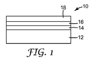
LITIドナーフィルム及びパターン形成
図1は、パターン形成されたLITIドナーフィルム10を図示する、側面図である。図1に示されるように、LITIドナーフィルム10は、典型的には、ドナー基材12、光熱変換(LTHC)層14、任意の中間層16、及び転写層18を含む。
LITI Donor Film and Patterning FIG. 1 is a side view illustrating a patterned
代表的なLITIドナーフィルムの様々な層及びそれを画像化する方法は、米国特許第6,866,979号、同第6,586,153号、同第6,468,715号、同第6,284,425号、及び同第5,725,989号により完全に記載され、これらのすべては、完全に説明されているかのように、参照により本明細書に組み込まれる。 Various layers of representative LITI donor films and methods for imaging them are described in US Pat. Nos. 6,866,979, 6,586,153, 6,468,715, , 284,425, and 5,725,989, all of which are incorporated herein by reference as if fully set forth.
ドナー基材12は、熱転写ドナー(フィルム10)の層に支持体を提供する。ポリマーフィルムの好適な種類の1つは、ポリエステルフィルム、例えば、ポリエチレンテレフタレート(PET)又はポリエチレンナフタレート(PEN)フィルムである。しかしながら、加熱及び転写に光が使用される場合、十分な光学的特性を有するその他のフィルムが使用されてもよい。ドナー基材は、少なくとも幾つかの場合において、均一なコーティングが形成され得るように、平坦である。ドナー基材はまた、典型的には、熱転写ドナー(例えば、LTHC層)中のいずれの層の加熱にかかわらず、安定した状態を保つ材料から選択される。より厚い又はより薄いドナー基材が使用されてもよいが、ドナー基材の好適な厚さは、例えば、0.025ミリメートル(mm)〜0.15mm、好ましくは0.05mm〜0.1mmである。
The
LTHC層14は、典型的には、転写層を熱転写ドナーから恒久レセプタに転写できるようにするために、入射光(例えば、レーザ光線)を吸収し、入射光の少なくとも一部分を熱に変換する、放射線吸収体を含む。あるいは、放射線吸収体は、LTHC層に加えて又はその代わりに、ドナーフィルムの1つ以上のその他の層に含まれてもよい。典型的には、LTHC層(又はその他の層)中の放射線吸収体は、電磁スペクトルの赤外線、可視線、及び/又は紫外線領域内の光を吸収する。放射線吸収体は、典型的には、選択される画像化放射線に対して極めて吸収性であり、0.2〜3、及び好ましくは0.5〜2の画像化放射線の波長で光学密度を提供する。好適な放射線吸収材料には、例えば、染料(例えば、可視染料、紫外線染料、赤外線染料、蛍光染料、及び放射線極性染料)、顔料、金属類、金属化合物類、金属フィルム、及びその他の好適な吸収材料を挙げることができる。その他の好適な放射線吸収体の例には、カーボンブラック、金属酸化物類、及び金属硫化物類を挙げることができる。
The
任意の中間層16は、熱転写ドナーにおいて転写層の転写される部分の損傷及び汚染を最小限にするために使用されてもよく、転写層の転写される部分中の変形を減少させてもよい。中間層はまた、転写層と熱転写ドナーの残りの部分との接着に影響を与えてもよい。典型的には、中間層は、高い耐熱性を有する。好ましくは、中間層は、画像化条件下において、転写される画像が機能しない状態になる程度まで変形又は化学的に分解しない。中間層は、典型的には、転写プロセス中、LTHC層と接触したままであり、転写層(例えば、ナノ構造化層及び所望により剥離層)によって実質的に転写されない。好適な中間層には、例えば、ポリマーフィルム、金属層(例えば、蒸着金属層)、無機層(例えば、ゾル−ゲル付着層及び無機酸化物類(例えば、シリカ、チタニア、及びその他の金属酸化物類)の蒸着層)、並びに有機/無機複合層が挙げられる。中間層材料として好適な有機材料としては、熱硬化性材料と熱可塑性材料との両方が挙げられる。好適な熱硬化性材料には、架橋された又は架橋可能なポリアクリレート類、ポリメタクリレート類、ポリエステル類、エポキシ類、及びポリウレタン類を含むが、これらに限定されない、熱、放射線、又は化学処理によって架橋することができる樹脂が挙げられる。熱硬化性材料は、例えば、熱可塑性前駆体としてLTHC層上にコーティングされ、続いて架橋されて、架橋された中間層を形成してもよい。中間層は、例えば、光開始剤、界面活性剤、色素、可塑剤、及びコーティング補助剤を含む添加剤を含んでもよい。
The optional
転写層18は、典型的には、レセプタに転写するための1つ以上の層を含む。これらの1つ以上の層は、有機、無機、有機金属、又はその他の材料を使用して形成されてもよい。有機材料には、例えば、小分子材料、ポリマー類、オリゴマー類、デンドリマー類、及び超分枝材料が挙げられる。熱転写層は、例えば、表示装置の発光素子、電子回路、レジスタ、コンデンサ、ダイオード、整流器、エレクトロルミネセントランプ、記憶素子、電解効果トランジスタ、バイポーラトランジスタ、単接トランジスタ、金属酸化物半導体(MOS)トランジスタ、金属−絶縁体−半導体トランジスタ、電化結合装置、絶縁体−金属−絶縁体積み重ね体、有機伝導体−金属−有機伝導体積み重ね体、集積回路、光検出器、レーザ、レンズ、導波管、格子、ホログラフィック素子、信号処理のためのフィルタ(例えば、アドドロップフィルタ、利得平坦化フィルタ、遮断フィルタ等)、光学フィルタ、鏡、スプリッタ、カップラー、結合器、モジュレータ、センサ(例えば、エバネセントセンサ、位相変調センサ、干渉センサ等)、光学キャビティ、圧電装置、強誘電体装置、薄膜電池、又はこれらの組み合わせ、例えば、光ディスプレイのための能動マトリックスアレイとしての電界効果トランジスタ及び有機エレクトロルミネセントランプの組み合わせを形成するために使用することができる転写層を含むことができる。その他の品目は、マルチコンポーネント転写アセンブリ又は単一層を転写することによって形成されてもよい。
The
転写層18を受容するための恒久レセプタは、透明なフィルム、ディスプレイ用ブラックマトリックス、電子ディスプレイ受動及び能動部分、金属類、半導体、ガラス、様々な紙、及びプラスチックを含むがこれらに限定されない、特定の用途に好適ないずれかの品目であってもよい。レセプタ基材の例には、陽極酸化アルミニウム及びその他の金属類、プラスチックフィルム(例えば、ポリエチレンテレフタレート、ポリプロピレン)、酸化インジウムスズでコーティングされたプラスチックフィルム、ガラス、酸化インジウムスズでコーティングされたガラス、フレキシブル回路、回路基板、ケイ素又はその他の半導体、及び様々な異なる種類の紙(例えば、充填若しくは未充填紙、光沢紙、又はコーティングされた紙)が挙げられる。
Permanent receptors for receiving the
放射線(例えば、光)を使用する熱転写では、LITIドナーフィルムとともに様々な放射線放出源が使用されてもよい。アナログ技術(例えば、マスクを通しての露光)、強力光源(例えば、キセノン閃光電球及びレーザ)が有用である。デジタル画像化技術では、赤外線、可視光線、及び紫外線レーザが特に有用である。好適なレーザには、例えば、高出力(例えば≧100mW)単一モード半導体レーザ、繊維結合半導体レーザ、及びダイオード励起固体レーザ(例えば、Nd:YAG及びNd:YLF)が挙げられる。レーザ曝露ドウェル時間は、例えば、約0.1マイクロ秒〜100マイクロ秒であってよく、レーザフルエンスは、例えば、約0.01J/cm2〜約1J/cm2であってよい。画像化中、熱転写層は、典型的には、転写層の少なくとも一部分を受容するように適合された恒久レセプタと密接に接触する。少なくとも幾つかの場合において、熱転写層のレセプタと密接に接触した状態を保つために、圧力又は真空が使用されてもよい。像様方法(例えば、デジタル的に、又はマスクを通したアナログ曝露による)でLTHC層又は放射線吸収体を含むその他の層を加熱して、熱転写層からレセプタへのパターンと一致する転写層の像様転写を実行するために、次いで、放射線源が使用されてもよい。 For thermal transfer using radiation (eg, light), various radiation emitting sources may be used with the LITI donor film. Analog technology (eg, exposure through a mask), intense light sources (eg, xenon flash bulbs and lasers) are useful. In digital imaging techniques, infrared, visible light, and ultraviolet lasers are particularly useful. Suitable lasers include, for example, high power (eg, ≧ 100 mW) single mode semiconductor lasers, fiber coupled semiconductor lasers, and diode pumped solid state lasers (eg, Nd: YAG and Nd: YLF). Laser exposure dwell time is, for example, be about 0.1 microseconds to 100 microseconds, the laser fluence, for example, may be about 0.01 J / cm 2 ~ about 1 J / cm 2. During imaging, the thermal transfer layer is typically in intimate contact with a permanent receptor adapted to receive at least a portion of the transfer layer. In at least some cases, pressure or vacuum may be used to remain in intimate contact with the receptor of the thermal transfer layer. An image of the transfer layer that matches the pattern from the thermal transfer layer to the receptor by heating the LTHC layer or other layer containing the radiation absorber in an imagewise manner (eg, digitally or by analog exposure through a mask). A radiation source may then be used to perform the like transfer.
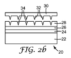
構造化転写層
図2a及び2bは、ツールでエンボス加工された転写層を含む、LITIドナーフィルム20を図示する。ドナーフィルム20は、基材22、LTHC層24、任意の中間層26、及び転写層28を含む。フィルム20において、基材22、LTHC 24、任意の中間層26、及び転写層28はそれぞれ、上述されるように及び構造化の前に、基材12、LTHC 14、中間層16、及び転写層18と一致してもよく、フィルム20は、上述される代表的な方法を使用して構成し、画像化することができる。
Structured Transfer Layer FIGS. 2a and 2b illustrate a
図2aに示されるように、ミクロ構造化又はナノ構造化形状32を有するツール30を使用して、転写層28の表面をエンボス加工する。ツールを使用するエンボス加工は、転写層としてポリマーコーティングが使用される場合に、特に有用である。エンボス加工の後、図2bに示されるように、転写層28は、転写層28に刻まれ形状32と一致するミクロ構造化又はナノ構造化形状34を有する。ツール30は、典型的には、機械加工金属材料から形成され、例えば、ワイヤ放電機械加工、ダイヤモンド旋盤機械加工、フライカッティング、ミリング、研削、彫刻、エッチング、フォトリソグラフィ、又はいずれかのマイクロ複写技術を使用して作製することができる。ツール30はまた、半導体装置製作プロセス又はレーザアブレーションを含む様々なその他のプロセスを使用し、硬いが非金属のツールから形成されてもよい。ツール30を使用して、転写層28を本質的にエンボス加工し、転写層の中に延びる形状34を生成することができる。例えば、圧力及び熱を使用してツール30を転写層28に対して定置し、転写層28の表面をエンボス加工してもよく、次いでツール30を、フィルム20を画像化する前に取り外す。
As shown in FIG. 2 a, the surface of the
ツール30の構造化部分32は、ミクロ構造化、ナノ構造化、又は両方の組み合わせであってよく、これらは、いずれかの二次元幾何学パターンで構成されてよい。パターンは、連続形状、不連続形状、又はこれらの組み合わせを含むことができる。不連続形状を使用して、例えば、ミクロ穿孔に沿って画像化される場合に、転写層の剥離を助長するミクロ穿孔を形成する。特に有用なパターンは、連続若しくは不連続形状のミクロ構造化又はナノ構造化タイルを形成する、実質的に矩形の形状の格子を含んでもよい。格子は、フィルム20を画像化する際に破断点を提供することができる。「破断点」という用語は、画像化される際の転写層の一部分の剥離を助長する領域を指し、例えば、これらは、転写層の最大厚さより薄い転写層の領域、又は転写層のその他の領域と比較してより容易に剥離する、転写層のより弱い領域を含むことができる。
The structured
ポリマー転写層に加え、無機(例えば、窒化ケイ素、酸化インジウムスズ、金属等)コーティングは、転写層を形成することができ、構造化することができる。可鍛性金属類は、転写層を形成する場合、ツール30に関して上述されるように、機械的エンボス加工によって構造化することができる。脆性無機材料(例えば、セラミック、ガラス等)は、転写層を形成する場合、レーザアブレーション等のその他の手段で構造化して、転写層にミクロ構造化又はナノ構造化パターンを形成することができる。レーザアブレーションの別の方法には、スクリーン様シャドーマスクによって無機材料をドナーフィルム上に付着させ、構造化転写層を形成する方法が挙げられる。もう1つの別の方法には、無機材料をドナーフィルム上へ付着させて転写層を形成し、次いで転写層材料に構造化パターンを生成するためにリソグラフィ方法を使用して、穿孔又は分離部をエッチングする方法が挙げられる。これらの方法は、例えば金属ホイルを転写するのに有用な手段を提供することができる。特に、金属ホイルは、転写層を形成するために付着された後、レーザエッチングされて破断点に形状を生成し、次いで破断点の一部分に沿って画像化されて金属ホイルの一部分を恒久レセプタに転写してもよい。別の方法として、金属ホイル又はその他の可溶性要素は、転写された破断点を除去し、転写されたタイル又はその他の構造体を溶解するために、焼結ないしは別の方法でこれらを処理することを伴う画像化後工程を受けることができ、本画像化後焼結工程は、転写された構造体を互いに物理接触させ、場合によってはこれらの間で電気信号を伝送できるようにすることができる。
In addition to the polymer transfer layer, inorganic (eg, silicon nitride, indium tin oxide, metal, etc.) coatings can form the transfer layer and can be structured. The malleable metals can be structured by mechanical embossing as described above with respect to the
図3は、転写層及び構造化中間層を含む、LITIドナーフィルム36を図示する。ドナーフィルム36は、基材38、LTHC層40、中間層42、及び転写層44を含む。フィルム36において、基材38、LTHC 40、中間層42、及び転写層44はそれぞれ、上述されるように及び構造化の前に、基材12、LTHC 14、中間層16、及び転写層18と一致してもよく、フィルム36は、上述される代表的な方法を使用して構成し、画像化することができる。中間層42は、転写層44に刻まれたミクロ構造化又はナノ構造化形状46を有する。中間層42は、様々な手段で構造化されてよい。例えば、上述されるように、構造化中間層の逆の表面形態を有するツールを使用して、ツール30が転写層をエンボス加工するために使用されるのと同一の方法で中間層42を構造化してもよい。転写層42が中間層42の上に適用される場合、転写層44の中に延びる形状46は、その中に破断点を生成する。中間層42は、ミクロ構造化又はナノ構造化形状のいずれかの二次元構成を有して生成されてもよい。別の方法として、中間層が使用されない場合、LTHC層は、構造体を転写層に付与するために、同一又は類似方法で構造化されてもよい。
FIG. 3 illustrates a
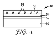
図4は、感光層からパターン形成される領域を有する転写層を含む、LITIドナーフィルム48を図示する。ドナーフィルム48は、基材50、LTHC層52、任意の中間層54、及び転写層56を含む。フィルム48において、基材50、LTHC 52、任意の中間層54、及び転写層56はそれぞれ、上述されるように及び構造化の前に、基材12、LTHC 14、中間層16、及び転写層18と一致してもよく、フィルム48は、上述される代表的な方法を使用して構成し、画像化することができる。一連のミクロ構造化又はナノ構造化領域58は、感光性中間層54中に生成される。転写層56の適用前、領域58は、感光性中間層54上への転写層56のコーティングを受けて、弱い部分、したがって破断点を生成するのに十分な強度及び持続時間の光に曝露される。例えば、領域58は、マスクを通して光に曝露されてもよい。これらの破断点は、画像化される際、転写層56の一部分の剥離を助長するために使用することができる。感光性中間層54は、ミクロ構造化又はナノ構造化領域のいずれかの二次元構成を有して生成されてもよい。
FIG. 4 illustrates a
上述される構造化転写層のいずれかは、追加の形状を含むことができる。例えば、これらは、フィルムに対する面内で等方性であり、面内方向に対して垂直なz方向に非等方性の複数の層を意味する、層状層を含むことができる。このような層の例は、米国特許第5,882,774(ジョンザ(Jonza)ら)に開示されるが、参照により本明細書に組み込まれる。転写層はまた、構造体パターン上に構造体を含むこともできる。例えば、これらは、ミクロ構造化形状の上にナノ構造化形状を有することができる。これらはまた、形状の種類の組み合わせを含むこともできる。例えば、転写層は、場合により、片側に構造化中間層を使用し、ツールを使用して反対側を構造化することによって、両側を構造化することができる。転写層のミクロ構造化又はナノ構造化形状は、規則的なパターン、不規則なパターン、ランダムパターン、又は擬似ランダムパターンで配置されてもよい。形状のパターンは、以下に更に記載されるように、連続であっても不連続であってもよい。形状のパターンは、恒久レセプタへの転写後、実質的に保持又は保存することができるが、必ずしもそうする必要はない。ミクロ構造化又はナノ構造化形状の形態は、転写層の特定の光学的又は機械的特性を提供するように構成することができる。 Any of the structured transfer layers described above can include additional shapes. For example, they can include layered layers, meaning a plurality of layers that are isotropic in the plane to the film and anisotropic in the z-direction perpendicular to the in-plane direction. Examples of such layers are disclosed in US Pat. No. 5,882,774 (Jonza et al.), Which is incorporated herein by reference. The transfer layer can also include a structure on the structure pattern. For example, they can have a nanostructured shape on top of a microstructured shape. They can also include combinations of shape types. For example, the transfer layer can optionally be structured on both sides by using a structured intermediate layer on one side and using a tool to structure the opposite side. The microstructured or nanostructured shape of the transfer layer may be arranged in a regular pattern, an irregular pattern, a random pattern, or a pseudo-random pattern. The pattern of shapes may be continuous or discontinuous, as further described below. The pattern of shapes can be substantially retained or preserved after transfer to the permanent receptor, but it is not necessary to do so. The morphology of the microstructured or nanostructured shape can be configured to provide specific optical or mechanical properties of the transfer layer.
ミクロ構造化又はナノ構造化形状は、実質的に均一な長さ及び形態であってもよいが、必ずしもそうである必要はない。形状の代表的な寸法は、面内方向(レーザビーム走査の平面に対して実質的に平行な方向)において、形状は、約0.01ミクロン〜100ミクロンであり、形状の高さ(面内方向に対して実質的に垂直なz方向)は、約1ナノメートル〜10ミクロン又は更には100ミクロンまでである。 A microstructured or nanostructured shape may be of substantially uniform length and form, but this is not necessarily so. Typical dimensions of the shape are in the in-plane direction (direction substantially parallel to the plane of laser beam scanning), the shape is about 0.01 microns to 100 microns, and the height of the shape (in-plane The z direction (substantially perpendicular to the direction) is from about 1 nanometer to 10 microns or even up to 100 microns.
図5aは、転写層の一部分を恒久レセプタ70に転写するために転写層を含む、LITIドナーフィルム60の画像化を図示する。図5b及び5cはそれぞれ、構造化転写層68の一部分の転写前及び後のLITIドナーフィルム60の画像化を図示する、平面図である。ドナーフィルム60は、基材62、LTHC層64、任意の中間層66、並びに上述され、破断線72及び74によって示されるもの等のミクロ構造化若しくはナノ構造化形状又は組み合わせを有する構造化転写層68を含む。フィルム60において、基材62、LTHC 64、及び任意の中間層66はそれぞれ、上述されるように、基材12、LTHC 14、及び中間層16と一致してもよく、転写層68は、上述される構造化転写層のいずれかと一致してもよい。転写層68は、構造化部分のいずれかの二次元構成を含むことができる。例えば、転写層68に形状を生成するために、上述される方法の1つを使用することによって、破断点72及び74で示されるような破断点を含むように構造化される。
FIG. 5 a illustrates imaging of a
レーザビーム76及び上述されるもの等の画像化方法を使用して破断点72及び74で画像化される際、部分78は、恒久レセプタ70に転写される。図5a及び5bに示されるように、破断点での画像化は、実際の画像化条件の代表的なものであることが意図され、レーザビームは、本明細書に記載される実施形態における画像化及びその他の構造化ドナーフィルムの画像化のために、破断点をわずかに超えて延びてもよい。図5a及び5cに示されるように、部分78は、構造化形状によって定められるパターンで転写され、好ましくは、転写される部分全体又は実質的にそのすべては、構造化形状によって定められるパターンを有する。画像化中、ドナーフィルム60は、典型的には、恒久レセプタ70と密接に接触した状態に保たれ、破断点72及び74は、部分78の転写層68からの剥離及び明確に定められた端部を、転写される部分78に提供することを助長する。
When imaged at
図6aは、転写層の一部分を構造化ツール90を有する恒久レセプタ92に転写するために、転写層を含むLITIドナーフィルム80の画像化を図示する。図6b及び6cはそれぞれ、転写層の一部分の構造化ツール90への転写前及び転写後のLITIドナーフィルム80の画像化を図示する、平面図である。ドナーフィルム80は、基材82、LTHC層84、任意の中間層86、及び転写層88を含む。フィルム80において、基材82、LTHC 84、任意の中間層86、及び転写層88はそれぞれ、上述されるように、基材12、LTHC 14、中間層16、及び転写層18と一致してもよく、転写層88は、上述されるように、任意に構造化されてよい。レセプタ92は、それに貼られたツール90を有し、ツール90は、ツールの表面から離れて延びる部分94及び96等のミクロ構造化又はナノ構造化形状を含む。ツール90の構造化部分は、いずれかの二次元パターンで配置されてよい。ツール90は、積層ないしは別の方法で、恒久的に又は取り外し可能な手段でレセプタ92に貼られてよい。
FIG. 6 a illustrates imaging of a
レーザビーム98及び上述されるもの等の画像化方法を使用して構造化部分94及び96で画像化される際、部分100は、恒久レセプタ92に転写される。示されるように、部分100は、ツールの構造化形状によって定められるパターンで転写され、転写される部分全体又は実質的にそのすべてが、ツールの構造化形状によって定められるパターンを有することが好ましい。画像化中、ドナーフィルム80は、典型的には、恒久レセプタ92と密接に接触した状態に保たれ、画像化の前にツール90に積層され、次いで画像化の後にツール90から取り外されてもよい。ツール90の構造化部分94及び96は、転写層88から部分100を剥離すること、及び明確に定められた端部を転写される部分100に提供することを助長するために、破断点を提供する。
When imaged with structured
画像化構造化パターンの実施例
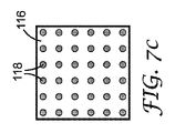
図7a〜7cは、走査されるレーザビームの幅より小さな寸法を有する不連続形状を転写するための、本発明の実施形態の使用を明示する、平面図である。図7aは、レーザによって走査される前にドナーフィルムの転写層110中の穿孔によって形状が定められる場合の形状112(この場合、円のパターン)を示す。図7bは、レーザがドナーフィルムを横断して走査する際に、レーザによって一掃されたパターン(濃い範囲114)を示す。図7cは、レーザ走査線114によって画像化された際にドナーフィルム110からレセプタ116に転写された形状(濃いスポット116)を示す。図7cの転写された形状118の大きさは、レーザビームの寸法によってというよりは、転写フィルム(形状112)の穿孔によって定められる。この均一な転写は、転写フィルム110とレーザ走査線114との間の横方向及び角度レジストレーションを必要とする。図7dは、転写フィルム形状112とレーザ走査線114との間に角度のずれがある場合に生じる、不均一な形状の転写を明示する。ずれのため、転写される部分118の多くは、図7dに示されるように、不完全な円でしかない。図7aのドナーフィルムに示される構造化パターンは、上述される代表的な技術を使用して形成することができ、ドナーフィルムは、上述される代表的な方法を使用して、画像化され、構造化パターンの少なくとも一部分をレセプタに転写することができる。
Examples of Imaging Structured Patterns FIGS. 7a-7c are plan views demonstrating the use of embodiments of the present invention to transfer discontinuous shapes having dimensions smaller than the width of the scanned laser beam. . FIG. 7a shows the shape 112 (in this case a circular pattern) where the shape is defined by perforations in the
図8a〜8cは、これらの連続形状が走査されるレーザビームの寸法より小さな細部を含むとしても、レーザ走査の方向に連続である形状を転写するための本発明の実施形態の使用を明示する、平面図である。図8aは、レーザによって走査される前に転写層120中の穿孔によって形状が定められる場合の形状122(この場合、直線ではない線)を示す。図8bは、レーザがドナーを横断して走査する際に、レーザによって一掃されたパターン(濃い範囲124)を示す。図8cは、レーザ走査線124によって画像化された際にドナーフィルム120からレセプタ126に転写された形状(濃い線128)を示す。転写された形状128中の細部(例えば、端部パターン)の大きさは、レーザビームの寸法によってというよりは、転写層の穿孔形状122によって定められる。この均一な転写は、転写フィルム120とレーザ走査線124との間の横方向及び角度レジストレーションを必要とする。図8aのドナーフィルムに示される構造化パターンは、上述される代表的な技術を使用して形成することができ、ドナーフィルムは、上述される代表的な方法を使用して、画像化され、構造化パターンの少なくとも一部分をレセプタに転写することができる。
Figures 8a-8c demonstrate the use of embodiments of the present invention to transfer shapes that are continuous in the direction of the laser scan, even though these continuous shapes include details that are smaller than the dimensions of the laser beam being scanned. FIG. FIG. 8a shows a shape 122 (in this case a non-straight line) where the shape is defined by perforations in the
図7d及び8cに図示されるように、転写層中の材料の強度によるが、転写層は、典型的には、画像化される際、走査線に沿って及び穿孔若しくは構造体で又はそれに沿ってのみ、レセプタに転写される。比較的弱いフィルム強度では、図7dの構造体に転写された不完全な円(完全な円112と比較して)及び図8cの転写された構造体の平坦な先端(鋭い先端を有する線122と比較して)によって示されるように、走査線及び構造体の両方に沿って転写することができる。あるいは、金属類等の比較的高いフィルム強度を有する材料では、転写層は、走査線によって部分的にのみ画像化されるとしても、構造体又は穿孔に沿って転写することができる。例えば、図7aの転写層材料が高いフィルム強度を有する場合、完全な円112の円の部分のみが走査線114内にあるとしても、これらの幾つかを転写することができ、図8aの転写層材料が高いフィルム強度を有する場合、線122の鋭い先端が走査線124内になくとも、これらの先端を転写することができる。
Depending on the strength of the material in the transfer layer as illustrated in FIGS. 7d and 8c, the transfer layer typically will be along the scan line and at or along the perforations or structures when imaged. Only transferred to the receptor. At relatively weak film strength, the imperfect circle transferred to the structure of FIG. 7d (compared to the perfect circle 112) and the flat tip (
図9a〜9cは、これらの不連続形状が走査されるレーザビームの寸法より小さな細部を含むとしても、レーザ走査の方向に不連続である形状を転写するための本発明の実施形態の使用を明示する、平面図である。図9aは、レーザによって走査される前に転写層130中の穿孔によって定められた際の形状132、この場合、正方形のきれいなタイル状の配列を示す。図9bは、レーザがドナーを横断して走査する際に、レーザによって一掃されたパターン(濃い範囲134)を示す。図9cは、レーザ走査線134によって画像化された際にドナーフィルム130からレセプタ136に転写された形状(小さな濃い正方形138)を示す。転写された形状138中の細部の大きさは、レーザビーム134の寸法によってというよりは、転写層の穿孔によって定められる。この均一な転写は、転写フィルム130とレーザ走査線134との間の横方向及び角度レジストレーションを必要とする。図9aのドナーフィルムに示される構造化パターンは、上述される代表的な技術を使用して形成することができ、ドナーフィルムは、上述される代表的な方法を使用して画像化し、構造化パターンの少なくとも一部分をレセプタに転写することができる。
FIGS. 9a-9c illustrate the use of embodiments of the present invention to transfer shapes that are discontinuous in the direction of laser scanning, even though these discontinuous shapes include details smaller than the size of the scanned laser beam. It is a plan view clearly showing. FIG. 9a shows a
図10a〜10dは、下に位置するレセプタ中のパターンと整合させるために、特定のパターンで形状を転写するための本発明の実施形態の使用を明示する、平面図である。図10aは、レーザによって走査される前に転写層140中の穿孔によって定められた際の形状142を示す。図10bは、レーザがドナーを横断して走査する際に、レーザによって一掃されたパターン(濃い範囲144)を示す。図10cは、転写された形状142が整合される、下に位置するレセプタ146中のパターン148を示す。図10dは、レーザ走査線144によって画像化された際にドナーフィルム140からレセプタ146に転写された形状(濃い領域150)を示す。本実施例において、転写された形状142は、必要に応じて、下に位置するレセプタの形状148の上に精密に定置されている。この均一な転写は、転写フィルム140とレーザ走査線144との間の横方向及び角度レジストレーションを必要とする。図10aのドナーフィルムに示される構造化パターンは、上述される代表的な技術を使用して形成することができ、ドナーフィルムは、上述される代表的な方法を使用して画像化し、構造化パターンの少なくとも一部分をレセプタに転写することができる。
Figures 10a to 10d are plan views demonstrating the use of embodiments of the present invention to transfer a shape with a particular pattern to align with the pattern in the underlying receptor. FIG. 10a shows the
図10a〜10dに示される実施例は、活性マトリックスディスプレイのバックプレーンのパターン形成と一致してもよい。この場合、レセプタ146は、バックプレーンであり、レセプタの形状148は、ディスプレイのサブピクセルである。それぞれのサブピクセルの上左角の「刻み目のある」部分は、サブピクセルの動作を制御するためのトランジスタを含む。転写層140は、サブピクセルの赤色、緑色、及び青色発光素子を形成するために、OLED材料等の材料を含む。転写層材料のレセプタ146への転写において、構造体142のパターンは、それぞれのサブピクセルのトランジスタによって占領される領域に材料を転写することなく、それぞれのサブピクセル150に精密に定置できるようにする。図10a〜10dに図示されるように、パターン形成された基材への転写はまた、平坦なパネルディスプレイ、液晶表示(LCD)装置に使用されるもの等のカラーフィルタ素子、蛍光素子、又はリン光素子等のカラーフィルタ素子を作製するための材料の転写に使用されてもよい。図10dに示されるパターンに加え、表示装置内のそれぞれのピクセルのサブピクセルの配置として既知のデルタパターンを有する基材に転写することができる。
The embodiment shown in FIGS. 10a-10d may be consistent with the patterning of the backplane of the active matrix display. In this case, the
したがって、図7a、8a、9a、及び10aのフィルムに示される構造体は、画像化される際、転写層中に穿孔を効果的に生成し、それらの一部分の剥離を助長することができる。構造体の特定の形態及びパターンは、例示目的のためだけに示され、その他の形態及びパターンが可能である。画像化される際、転写層中の材料強度によるが、転写層は、典型的には、穿孔若しくは構造体で又はそれに沿ってのみレセプタに転写する。例えば、金属類又は脆性材料等の特定の材料は、それらの画像化が、構造体によってもたらされる破断点の効果がなければ転写層の一部分を転写しないほどの十分な強度を有する。構造体のパターンは、これらの種類の材料の画像化及び転写、並びに様々なパターンでの転写を可能にする。したがって、図7c、7d、8c、9c、及び10dに図示されるように、転写された部分は、構造化形状によって定められるパターンを有し、好ましくは、転写された部分全体又はその実質的にすべては、構造化形状によって定められるパターンを有する。その他の場合において、転写層は、より弱い材料から構成される場合、穿孔及び走査レーザビームの端部の両方に沿って転写することができる。 Thus, the structures shown in the films of FIGS. 7a, 8a, 9a, and 10a, when imaged, can effectively create perforations in the transfer layer and help exfoliate portions of them. The specific forms and patterns of the structures are shown for illustrative purposes only, and other forms and patterns are possible. When imaged, depending on the material strength in the transfer layer, the transfer layer typically transfers to the receptor only in or along perforations or structures. For example, certain materials, such as metals or brittle materials, are sufficiently strong that their imaging does not transfer a portion of the transfer layer without the effect of breakpoints provided by the structure. The pattern of the structure allows for the imaging and transfer of these types of materials as well as transfer in various patterns. Thus, as illustrated in FIGS. 7c, 7d, 8c, 9c, and 10d, the transferred portion has a pattern defined by the structured shape, and preferably the entire transferred portion or substantially its entirety. All have a pattern defined by a structured shape. In other cases, if the transfer layer is composed of a weaker material, it can be transferred along both the perforation and the edge of the scanning laser beam.
以上、例示的実施形態に関連して本発明を説明したが、当業者には多くの修正が容易に明らかであり、本願は、例示的実施形態のあらゆる適合例及び変形例を包含することを意図したものであることが理解されよう。例えば、本発明の範囲から逸脱することなく、様々な種類の転写層及びレセプタのパターンが使用されてもよい。本発明は、特許請求の範囲及びその等価物によってのみ限定されるべきである。 While the invention has been described with reference to exemplary embodiments, many modifications will be readily apparent to those skilled in the art, and this application is intended to cover all adaptations and variations of the exemplary embodiments. It will be understood that it is intended. For example, various types of transfer layer and receptor patterns may be used without departing from the scope of the present invention. The present invention should be limited only by the claims and the equivalents thereof.
Claims (2)
基材と、
前記基材の上に位置する光熱変換層と、
前記光熱変換層の上に位置する転写層と、を含み、
前記転写層の表面が、前記転写層の中に延びる複数個のミクロ構造化又はナノ構造化形状を含み、前記ドナーフィルムが、前記形状によって定められるパターンで前記転写層の少なくとも一部分をレセプタに転写するように構成され、配置され、前記ドナーフィルムが、前記形状によって定められるパターンによって前記転写層の前記レセプタに転写される部分に破断線を含み、
前記パターンは、活性マトリックスディスプレイのサブピクセルである
レーザ誘起熱転写(LITI)ドナーフィルム。 A laser induced thermal transfer (LITI) donor film,
A substrate;
A photothermal conversion layer positioned on the substrate;
A transfer layer located on the photothermal conversion layer,
A surface of the transfer layer includes a plurality of microstructured or nanostructured shapes extending into the transfer layer, and the donor film transfers at least a portion of the transfer layer to a receptor in a pattern defined by the shape. is configured to, being arranged, the donor film is seen containing a broken line by the pattern defined by the shape portion is transferred to the receptor of the transfer layer,
The pattern is a laser induced thermal transfer (LITI) donor film that is a subpixel of an active matrix display .
基材と、
前記基材の上に位置する光熱変換層と、
前記光熱変換層の上に位置する転写層であって、前記転写層の表面が、前記転写層の中に延びる複数個のミクロ構造化又はナノ構造化形状を含む、転写層と、を含む、レーザ誘起熱転写(LITI)ドナーフィルムを提供する工程と、
前記転写層が前記レセプタの表面と接触するように、前記LITIドナーフィルムを恒久レセプタの表面に対して定置する工程と、
前記形状によって定められるパターンで、前記転写層の少なくとも一部分を前記恒久レセプタの表面に選択的に転写する工程と、
を含み、前記ドナーフィルムが、前記形状によって定められるパターンによって前記転写層の前記レセプタに転写される部分に破断線を含み、
前記パターンは、活性マトリックスディスプレイのサブピクセルである
方法。 A method of making a microstructured or nanostructured article comprising:
A substrate;
A photothermal conversion layer positioned on the substrate;
A transfer layer positioned over the photothermal conversion layer, wherein the transfer layer surface includes a plurality of microstructured or nanostructured shapes extending into the transfer layer; and Providing a laser induced thermal transfer (LITI) donor film;
Placing the LITI donor film against the surface of a permanent receptor such that the transfer layer contacts the surface of the receptor;
Selectively transferring at least a portion of the transfer layer to the surface of the permanent receptor in a pattern defined by the shape;
Hints, the donor film is seen containing a broken line by the pattern defined by the shape portion is transferred to the receptor of the transfer layer,
The method wherein the pattern is a sub-pixel of an active matrix display .
Applications Claiming Priority (3)
| Application Number | Priority Date | Filing Date | Title |
|---|---|---|---|
| US11/551,276 US7419757B2 (en) | 2006-10-20 | 2006-10-20 | Structured thermal transfer donors |
| US11/551,276 | 2006-10-20 | ||
| PCT/US2007/081336 WO2008048913A1 (en) | 2006-10-20 | 2007-10-15 | Structured thermal transfer donors |
Related Child Applications (1)
| Application Number | Title | Priority Date | Filing Date |
|---|---|---|---|
| JP2013094967A Division JP5662514B2 (en) | 2006-10-20 | 2013-04-30 | Structured thermal transfer donor |
Publications (3)
| Publication Number | Publication Date |
|---|---|
| JP2010506771A JP2010506771A (en) | 2010-03-04 |
| JP2010506771A5 JP2010506771A5 (en) | 2010-11-25 |
| JP5496673B2 true JP5496673B2 (en) | 2014-05-21 |
Family
ID=39314353
Family Applications (2)
| Application Number | Title | Priority Date | Filing Date |
|---|---|---|---|
| JP2009533458A Active JP5496673B2 (en) | 2006-10-20 | 2007-10-15 | Structured thermal transfer donor |
| JP2013094967A Active JP5662514B2 (en) | 2006-10-20 | 2013-04-30 | Structured thermal transfer donor |
Family Applications After (1)
| Application Number | Title | Priority Date | Filing Date |
|---|---|---|---|
| JP2013094967A Active JP5662514B2 (en) | 2006-10-20 | 2013-04-30 | Structured thermal transfer donor |
Country Status (5)
| Country | Link |
|---|---|
| US (2) | US7419757B2 (en) |
| JP (2) | JP5496673B2 (en) |
| KR (1) | KR101358783B1 (en) |
| TW (1) | TWI474756B (en) |
| WO (1) | WO2008048913A1 (en) |
Families Citing this family (9)
| Publication number | Priority date | Publication date | Assignee | Title |
|---|---|---|---|---|
| US7419757B2 (en) * | 2006-10-20 | 2008-09-02 | 3M Innovative Properties Company | Structured thermal transfer donors |
| US20080233404A1 (en) * | 2007-03-22 | 2008-09-25 | 3M Innovative Properties Company | Microreplication tools and patterns using laser induced thermal embossing |
| US8182633B2 (en) * | 2008-04-29 | 2012-05-22 | Samsung Electronics Co., Ltd. | Method of fabricating a flexible display device |
| KR101803724B1 (en) * | 2011-06-16 | 2017-12-04 | 삼성디스플레이 주식회사 | Organic light emitting structure, method of manufacturing an organic light emitting structure, organic light emitting display device and method of manufacturing an organic light emitting display device |
| JP5982146B2 (en) * | 2011-06-16 | 2016-08-31 | 三星ディスプレイ株式會社Samsung Display Co.,Ltd. | Organic light emitting structure, method for manufacturing organic light emitting structure, organic light emitting display device, and method for manufacturing organic light emitting display |
| US9780335B2 (en) * | 2012-07-20 | 2017-10-03 | 3M Innovative Properties Company | Structured lamination transfer films and methods |
| KR20150012530A (en) | 2013-07-25 | 2015-02-04 | 삼성디스플레이 주식회사 | Donor substrate for trnasfer and manufacturing method of organic light emitting diode display |
| JP6016754B2 (en) | 2013-11-15 | 2016-10-26 | オムロンオートモーティブエレクトロニクス株式会社 | Battery voltage detector |
| DE102014210798A1 (en) | 2014-06-05 | 2015-12-17 | Fraunhofer-Gesellschaft zur Förderung der angewandten Forschung e.V. | Mold, process for its manufacture and use, and plastic film and plastic component |
Family Cites Families (24)
| Publication number | Priority date | Publication date | Assignee | Title |
|---|---|---|---|---|
| JPS5949919B2 (en) * | 1979-03-13 | 1984-12-05 | 東洋メタライジング株式会社 | Transfer sheet with pattern |
| CA2173855C (en) * | 1993-10-29 | 2007-06-26 | Mieczyslaw H. Mazurek | Pressure-sensitive adhesives having microstructured surfaces |
| US5882774A (en) * | 1993-12-21 | 1999-03-16 | Minnesota Mining And Manufacturing Company | Optical film |
| US5725989A (en) * | 1996-04-15 | 1998-03-10 | Chang; Jeffrey C. | Laser addressable thermal transfer imaging element with an interlayer |
| US6197397B1 (en) * | 1996-12-31 | 2001-03-06 | 3M Innovative Properties Company | Adhesives having a microreplicated topography and methods of making and using same |
| JPH11142633A (en) * | 1997-11-05 | 1999-05-28 | Alps Electric Co Ltd | Production of color filter |
| US6114088A (en) * | 1999-01-15 | 2000-09-05 | 3M Innovative Properties Company | Thermal transfer element for forming multilayer devices |
| JP2000255015A (en) * | 1999-03-10 | 2000-09-19 | Mitsubishi Polyester Film Copp | Cover film for dry film resist |
| US6524675B1 (en) * | 1999-05-13 | 2003-02-25 | 3M Innovative Properties Company | Adhesive-back articles |
| US6560215B1 (en) * | 1999-08-24 | 2003-05-06 | Motorola, Inc. | Method and apparatus for updating a timing offset in a communication device |
| JP4590663B2 (en) * | 1999-10-29 | 2010-12-01 | セイコーエプソン株式会社 | Manufacturing method of color filter |
| US6521324B1 (en) * | 1999-11-30 | 2003-02-18 | 3M Innovative Properties Company | Thermal transfer of microstructured layers |
| US6284425B1 (en) * | 1999-12-28 | 2001-09-04 | 3M Innovative Properties | Thermal transfer donor element having a heat management underlayer |
| US6228555B1 (en) * | 1999-12-28 | 2001-05-08 | 3M Innovative Properties Company | Thermal mass transfer donor element |
| US6855384B1 (en) * | 2000-09-15 | 2005-02-15 | 3M Innovative Properties Company | Selective thermal transfer of light emitting polymer blends |
| JP2003168559A (en) * | 2001-11-30 | 2003-06-13 | Sharp Corp | Organic led donor film and substrate, and organic led display panel using the same and its manufacturing method |
| JP5022552B2 (en) * | 2002-09-26 | 2012-09-12 | セイコーエプソン株式会社 | Electro-optical device manufacturing method and electro-optical device |
| US20040067302A1 (en) * | 2002-10-08 | 2004-04-08 | Eastman Kodak Company | Laser thermal transfer gap control for oled manufacturing |
| KR100552964B1 (en) * | 2003-08-28 | 2006-02-15 | 삼성에스디아이 주식회사 | donor film for flat panel display device and method of fabricating OLED using the same |
| KR100635057B1 (en) | 2004-02-20 | 2006-10-17 | 삼성에스디아이 주식회사 | Method of fabricating donor film for flat panel display device and method of fabricating OLED using the same |
| KR20060020030A (en) * | 2004-08-30 | 2006-03-06 | 삼성에스디아이 주식회사 | Fabricating method of donor device |
| KR100793355B1 (en) * | 2004-10-05 | 2008-01-11 | 삼성에스디아이 주식회사 | Fabricating method of donor device and fabricating method of OLED using the donor device |
| KR20060089838A (en) | 2005-02-04 | 2006-08-09 | 삼성에스디아이 주식회사 | Donor film for thin film transfer |
| US7419757B2 (en) * | 2006-10-20 | 2008-09-02 | 3M Innovative Properties Company | Structured thermal transfer donors |
-
2006
- 2006-10-20 US US11/551,276 patent/US7419757B2/en active Active
-
2007
- 2007-10-15 WO PCT/US2007/081336 patent/WO2008048913A1/en active Application Filing
- 2007-10-15 JP JP2009533458A patent/JP5496673B2/en active Active
- 2007-10-15 KR KR1020097008557A patent/KR101358783B1/en active IP Right Grant
- 2007-10-19 TW TW96139376A patent/TWI474756B/en active
-
2008
- 2008-07-29 US US12/181,398 patent/US7592120B2/en active Active
-
2013
- 2013-04-30 JP JP2013094967A patent/JP5662514B2/en active Active
Also Published As
| Publication number | Publication date |
|---|---|
| KR20090077928A (en) | 2009-07-16 |
| US7419757B2 (en) | 2008-09-02 |
| JP2013237268A (en) | 2013-11-28 |
| TW200836582A (en) | 2008-09-01 |
| JP5662514B2 (en) | 2015-01-28 |
| JP2010506771A (en) | 2010-03-04 |
| US20080286681A1 (en) | 2008-11-20 |
| US7592120B2 (en) | 2009-09-22 |
| TWI474756B (en) | 2015-02-21 |
| US20080096124A1 (en) | 2008-04-24 |
| KR101358783B1 (en) | 2014-02-07 |
| WO2008048913A1 (en) | 2008-04-24 |
Similar Documents
| Publication | Publication Date | Title |
|---|---|---|
| JP5662514B2 (en) | Structured thermal transfer donor | |
| JP5475474B2 (en) | Microreplication tools and patterns using laser-induced hot embossing | |
| TWI432921B (en) | Donor films with pattern-directing layers | |
| KR100698336B1 (en) | Thermal transfer of microstructured layers | |
| US7259106B2 (en) | Method of making a microelectronic and/or optoelectronic circuitry sheet | |
| US20110207328A1 (en) | Methods and apparatus for the manufacture of microstructures | |
| JP2009510521A (en) | Laser resist transfer for micro assembly | |
| WO2013089138A1 (en) | Deposition mask and manufacturing method for deposition mask | |
| WO2013010113A1 (en) | Non-contact transfer printing | |
| WO1999045593A1 (en) | Three-dimensional device | |
| JP2008226877A (en) | Process for fabricating electronic device | |
| JP6742711B2 (en) | Method for transferring fine pattern to surface uneven surface treated object using film for attaching uneven surface | |
| KR100761073B1 (en) | Laser induced thermal imaging method | |
| KR20060018159A (en) | Donor device and liti method using the donor device | |
| KR20120083761A (en) | Cliche and method for preparing the same |
Legal Events
| Date | Code | Title | Description |
|---|---|---|---|
| A521 | Request for written amendment filed |
Free format text: JAPANESE INTERMEDIATE CODE: A523 Effective date: 20100929 |
|
| A621 | Written request for application examination |
Free format text: JAPANESE INTERMEDIATE CODE: A621 Effective date: 20100929 |
|
| A711 | Notification of change in applicant |
Free format text: JAPANESE INTERMEDIATE CODE: A711 Effective date: 20101221 |
|
| A711 | Notification of change in applicant |
Free format text: JAPANESE INTERMEDIATE CODE: A712 Effective date: 20120921 |
|
| A977 | Report on retrieval |
Free format text: JAPANESE INTERMEDIATE CODE: A971007 Effective date: 20120926 |
|
| A131 | Notification of reasons for refusal |
Free format text: JAPANESE INTERMEDIATE CODE: A131 Effective date: 20130129 |
|
| A521 | Request for written amendment filed |
Free format text: JAPANESE INTERMEDIATE CODE: A523 Effective date: 20130430 |
|
| A02 | Decision of refusal |
Free format text: JAPANESE INTERMEDIATE CODE: A02 Effective date: 20130723 |
|
| A521 | Request for written amendment filed |
Free format text: JAPANESE INTERMEDIATE CODE: A523 Effective date: 20131125 |
|
| A911 | Transfer to examiner for re-examination before appeal (zenchi) |
Free format text: JAPANESE INTERMEDIATE CODE: A911 Effective date: 20131202 |
|
| TRDD | Decision of grant or rejection written | ||
| A01 | Written decision to grant a patent or to grant a registration (utility model) |
Free format text: JAPANESE INTERMEDIATE CODE: A01 Effective date: 20140204 |
|
| A61 | First payment of annual fees (during grant procedure) |
Free format text: JAPANESE INTERMEDIATE CODE: A61 Effective date: 20140305 |
|
| R150 | Certificate of patent or registration of utility model |
Ref document number: 5496673 Country of ref document: JP Free format text: JAPANESE INTERMEDIATE CODE: R150 |
|
| R250 | Receipt of annual fees |
Free format text: JAPANESE INTERMEDIATE CODE: R250 |
|
| R250 | Receipt of annual fees |
Free format text: JAPANESE INTERMEDIATE CODE: R250 |
|
| R250 | Receipt of annual fees |
Free format text: JAPANESE INTERMEDIATE CODE: R250 |
|
| R250 | Receipt of annual fees |
Free format text: JAPANESE INTERMEDIATE CODE: R250 |
|
| R250 | Receipt of annual fees |
Free format text: JAPANESE INTERMEDIATE CODE: R250 |
|
| R250 | Receipt of annual fees |
Free format text: JAPANESE INTERMEDIATE CODE: R250 |
|
| R250 | Receipt of annual fees |
Free format text: JAPANESE INTERMEDIATE CODE: R250 |
|
| R250 | Receipt of annual fees |
Free format text: JAPANESE INTERMEDIATE CODE: R250 |