JP5489724B2 - Reduction of line end shortening during etching - Google Patents
Reduction of line end shortening during etching Download PDFInfo
- Publication number
- JP5489724B2 JP5489724B2 JP2009545644A JP2009545644A JP5489724B2 JP 5489724 B2 JP5489724 B2 JP 5489724B2 JP 2009545644 A JP2009545644 A JP 2009545644A JP 2009545644 A JP2009545644 A JP 2009545644A JP 5489724 B2 JP5489724 B2 JP 5489724B2
- Authority
- JP
- Japan
- Prior art keywords
- gas
- photoresist
- line
- trimming
- layer
- Prior art date
- Legal status (The legal status is an assumption and is not a legal conclusion. Google has not performed a legal analysis and makes no representation as to the accuracy of the status listed.)
- Expired - Fee Related
Links
Images


Classifications
-
- H—ELECTRICITY
- H01—ELECTRIC ELEMENTS
- H01L—SEMICONDUCTOR DEVICES NOT COVERED BY CLASS H10
- H01L21/00—Processes or apparatus adapted for the manufacture or treatment of semiconductor or solid state devices or of parts thereof
- H01L21/02—Manufacture or treatment of semiconductor devices or of parts thereof
- H01L21/02104—Forming layers
- H01L21/02107—Forming insulating materials on a substrate
- H01L21/02225—Forming insulating materials on a substrate characterised by the process for the formation of the insulating layer
- H01L21/0226—Forming insulating materials on a substrate characterised by the process for the formation of the insulating layer formation by a deposition process
- H01L21/02263—Forming insulating materials on a substrate characterised by the process for the formation of the insulating layer formation by a deposition process deposition from the gas or vapour phase
- H01L21/02271—Forming insulating materials on a substrate characterised by the process for the formation of the insulating layer formation by a deposition process deposition from the gas or vapour phase deposition by decomposition or reaction of gaseous or vapour phase compounds, i.e. chemical vapour deposition
- H01L21/02274—Forming insulating materials on a substrate characterised by the process for the formation of the insulating layer formation by a deposition process deposition from the gas or vapour phase deposition by decomposition or reaction of gaseous or vapour phase compounds, i.e. chemical vapour deposition in the presence of a plasma [PECVD]
-
- H—ELECTRICITY
- H01—ELECTRIC ELEMENTS
- H01L—SEMICONDUCTOR DEVICES NOT COVERED BY CLASS H10
- H01L21/00—Processes or apparatus adapted for the manufacture or treatment of semiconductor or solid state devices or of parts thereof
- H01L21/02—Manufacture or treatment of semiconductor devices or of parts thereof
- H01L21/04—Manufacture or treatment of semiconductor devices or of parts thereof the devices having at least one potential-jump barrier or surface barrier, e.g. PN junction, depletion layer or carrier concentration layer
- H01L21/18—Manufacture or treatment of semiconductor devices or of parts thereof the devices having at least one potential-jump barrier or surface barrier, e.g. PN junction, depletion layer or carrier concentration layer the devices having semiconductor bodies comprising elements of Group IV of the Periodic System or AIIIBV compounds with or without impurities, e.g. doping materials
- H01L21/30—Treatment of semiconductor bodies using processes or apparatus not provided for in groups H01L21/20 - H01L21/26
- H01L21/31—Treatment of semiconductor bodies using processes or apparatus not provided for in groups H01L21/20 - H01L21/26 to form insulating layers thereon, e.g. for masking or by using photolithographic techniques; After treatment of these layers; Selection of materials for these layers
- H01L21/3105—After-treatment
- H01L21/311—Etching the insulating layers by chemical or physical means
- H01L21/31144—Etching the insulating layers by chemical or physical means using masks
-
- G—PHYSICS
- G03—PHOTOGRAPHY; CINEMATOGRAPHY; ANALOGOUS TECHNIQUES USING WAVES OTHER THAN OPTICAL WAVES; ELECTROGRAPHY; HOLOGRAPHY
- G03F—PHOTOMECHANICAL PRODUCTION OF TEXTURED OR PATTERNED SURFACES, e.g. FOR PRINTING, FOR PROCESSING OF SEMICONDUCTOR DEVICES; MATERIALS THEREFOR; ORIGINALS THEREFOR; APPARATUS SPECIALLY ADAPTED THEREFOR
- G03F7/00—Photomechanical, e.g. photolithographic, production of textured or patterned surfaces, e.g. printing surfaces; Materials therefor, e.g. comprising photoresists; Apparatus specially adapted therefor
- G03F7/70—Microphotolithographic exposure; Apparatus therefor
- G03F7/70483—Information management; Active and passive control; Testing; Wafer monitoring, e.g. pattern monitoring
- G03F7/70491—Information management, e.g. software; Active and passive control, e.g. details of controlling exposure processes or exposure tool monitoring processes
- G03F7/705—Modelling or simulating from physical phenomena up to complete wafer processes or whole workflow in wafer productions
-
- G—PHYSICS
- G03—PHOTOGRAPHY; CINEMATOGRAPHY; ANALOGOUS TECHNIQUES USING WAVES OTHER THAN OPTICAL WAVES; ELECTROGRAPHY; HOLOGRAPHY
- G03F—PHOTOMECHANICAL PRODUCTION OF TEXTURED OR PATTERNED SURFACES, e.g. FOR PRINTING, FOR PROCESSING OF SEMICONDUCTOR DEVICES; MATERIALS THEREFOR; ORIGINALS THEREFOR; APPARATUS SPECIALLY ADAPTED THEREFOR
- G03F7/00—Photomechanical, e.g. photolithographic, production of textured or patterned surfaces, e.g. printing surfaces; Materials therefor, e.g. comprising photoresists; Apparatus specially adapted therefor
- G03F7/70—Microphotolithographic exposure; Apparatus therefor
- G03F7/70691—Handling of masks or workpieces
-
- H—ELECTRICITY
- H01—ELECTRIC ELEMENTS
- H01L—SEMICONDUCTOR DEVICES NOT COVERED BY CLASS H10
- H01L21/00—Processes or apparatus adapted for the manufacture or treatment of semiconductor or solid state devices or of parts thereof
- H01L21/02—Manufacture or treatment of semiconductor devices or of parts thereof
- H01L21/02104—Forming layers
- H01L21/02107—Forming insulating materials on a substrate
- H01L21/02109—Forming insulating materials on a substrate characterised by the type of layer, e.g. type of material, porous/non-porous, pre-cursors, mixtures or laminates
- H01L21/02112—Forming insulating materials on a substrate characterised by the type of layer, e.g. type of material, porous/non-porous, pre-cursors, mixtures or laminates characterised by the material of the layer
- H01L21/02118—Forming insulating materials on a substrate characterised by the type of layer, e.g. type of material, porous/non-porous, pre-cursors, mixtures or laminates characterised by the material of the layer carbon based polymeric organic or inorganic material, e.g. polyimides, poly cyclobutene or PVC
- H01L21/0212—Forming insulating materials on a substrate characterised by the type of layer, e.g. type of material, porous/non-porous, pre-cursors, mixtures or laminates characterised by the material of the layer carbon based polymeric organic or inorganic material, e.g. polyimides, poly cyclobutene or PVC the material being fluoro carbon compounds, e.g.(CFx) n, (CHxFy) n or polytetrafluoroethylene
-
- H—ELECTRICITY
- H01—ELECTRIC ELEMENTS
- H01L—SEMICONDUCTOR DEVICES NOT COVERED BY CLASS H10
- H01L21/00—Processes or apparatus adapted for the manufacture or treatment of semiconductor or solid state devices or of parts thereof
- H01L21/02—Manufacture or treatment of semiconductor devices or of parts thereof
- H01L21/02104—Forming layers
- H01L21/02107—Forming insulating materials on a substrate
- H01L21/02225—Forming insulating materials on a substrate characterised by the process for the formation of the insulating layer
- H01L21/0226—Forming insulating materials on a substrate characterised by the process for the formation of the insulating layer formation by a deposition process
- H01L21/02263—Forming insulating materials on a substrate characterised by the process for the formation of the insulating layer formation by a deposition process deposition from the gas or vapour phase
- H01L21/02271—Forming insulating materials on a substrate characterised by the process for the formation of the insulating layer formation by a deposition process deposition from the gas or vapour phase deposition by decomposition or reaction of gaseous or vapour phase compounds, i.e. chemical vapour deposition
- H01L21/0228—Forming insulating materials on a substrate characterised by the process for the formation of the insulating layer formation by a deposition process deposition from the gas or vapour phase deposition by decomposition or reaction of gaseous or vapour phase compounds, i.e. chemical vapour deposition deposition by cyclic CVD, e.g. ALD, ALE, pulsed CVD
-
- H—ELECTRICITY
- H01—ELECTRIC ELEMENTS
- H01L—SEMICONDUCTOR DEVICES NOT COVERED BY CLASS H10
- H01L21/00—Processes or apparatus adapted for the manufacture or treatment of semiconductor or solid state devices or of parts thereof
- H01L21/02—Manufacture or treatment of semiconductor devices or of parts thereof
- H01L21/02104—Forming layers
- H01L21/02107—Forming insulating materials on a substrate
- H01L21/02296—Forming insulating materials on a substrate characterised by the treatment performed before or after the formation of the layer
- H01L21/02318—Forming insulating materials on a substrate characterised by the treatment performed before or after the formation of the layer post-treatment
- H01L21/02337—Forming insulating materials on a substrate characterised by the treatment performed before or after the formation of the layer post-treatment treatment by exposure to a gas or vapour
- H01L21/0234—Forming insulating materials on a substrate characterised by the treatment performed before or after the formation of the layer post-treatment treatment by exposure to a gas or vapour treatment by exposure to a plasma
-
- H—ELECTRICITY
- H01—ELECTRIC ELEMENTS
- H01L—SEMICONDUCTOR DEVICES NOT COVERED BY CLASS H10
- H01L21/00—Processes or apparatus adapted for the manufacture or treatment of semiconductor or solid state devices or of parts thereof
- H01L21/02—Manufacture or treatment of semiconductor devices or of parts thereof
- H01L21/027—Making masks on semiconductor bodies for further photolithographic processing not provided for in group H01L21/18 or H01L21/34
- H01L21/0271—Making masks on semiconductor bodies for further photolithographic processing not provided for in group H01L21/18 or H01L21/34 comprising organic layers
- H01L21/0273—Making masks on semiconductor bodies for further photolithographic processing not provided for in group H01L21/18 or H01L21/34 comprising organic layers characterised by the treatment of photoresist layers
-
- H—ELECTRICITY
- H01—ELECTRIC ELEMENTS
- H01L—SEMICONDUCTOR DEVICES NOT COVERED BY CLASS H10
- H01L21/00—Processes or apparatus adapted for the manufacture or treatment of semiconductor or solid state devices or of parts thereof
- H01L21/02—Manufacture or treatment of semiconductor devices or of parts thereof
- H01L21/04—Manufacture or treatment of semiconductor devices or of parts thereof the devices having at least one potential-jump barrier or surface barrier, e.g. PN junction, depletion layer or carrier concentration layer
- H01L21/18—Manufacture or treatment of semiconductor devices or of parts thereof the devices having at least one potential-jump barrier or surface barrier, e.g. PN junction, depletion layer or carrier concentration layer the devices having semiconductor bodies comprising elements of Group IV of the Periodic System or AIIIBV compounds with or without impurities, e.g. doping materials
- H01L21/30—Treatment of semiconductor bodies using processes or apparatus not provided for in groups H01L21/20 - H01L21/26
- H01L21/31—Treatment of semiconductor bodies using processes or apparatus not provided for in groups H01L21/20 - H01L21/26 to form insulating layers thereon, e.g. for masking or by using photolithographic techniques; After treatment of these layers; Selection of materials for these layers
- H01L21/3105—After-treatment
- H01L21/31058—After-treatment of organic layers
-
- H—ELECTRICITY
- H01—ELECTRIC ELEMENTS
- H01L—SEMICONDUCTOR DEVICES NOT COVERED BY CLASS H10
- H01L21/00—Processes or apparatus adapted for the manufacture or treatment of semiconductor or solid state devices or of parts thereof
- H01L21/02—Manufacture or treatment of semiconductor devices or of parts thereof
- H01L21/04—Manufacture or treatment of semiconductor devices or of parts thereof the devices having at least one potential-jump barrier or surface barrier, e.g. PN junction, depletion layer or carrier concentration layer
- H01L21/18—Manufacture or treatment of semiconductor devices or of parts thereof the devices having at least one potential-jump barrier or surface barrier, e.g. PN junction, depletion layer or carrier concentration layer the devices having semiconductor bodies comprising elements of Group IV of the Periodic System or AIIIBV compounds with or without impurities, e.g. doping materials
- H01L21/30—Treatment of semiconductor bodies using processes or apparatus not provided for in groups H01L21/20 - H01L21/26
- H01L21/31—Treatment of semiconductor bodies using processes or apparatus not provided for in groups H01L21/20 - H01L21/26 to form insulating layers thereon, e.g. for masking or by using photolithographic techniques; After treatment of these layers; Selection of materials for these layers
- H01L21/312—Organic layers, e.g. photoresist
- H01L21/3127—Layers comprising fluoro (hydro)carbon compounds, e.g. polytetrafluoroethylene
-
- H—ELECTRICITY
- H01—ELECTRIC ELEMENTS
- H01L—SEMICONDUCTOR DEVICES NOT COVERED BY CLASS H10
- H01L21/00—Processes or apparatus adapted for the manufacture or treatment of semiconductor or solid state devices or of parts thereof
- H01L21/02—Manufacture or treatment of semiconductor devices or of parts thereof
- H01L21/04—Manufacture or treatment of semiconductor devices or of parts thereof the devices having at least one potential-jump barrier or surface barrier, e.g. PN junction, depletion layer or carrier concentration layer
- H01L21/18—Manufacture or treatment of semiconductor devices or of parts thereof the devices having at least one potential-jump barrier or surface barrier, e.g. PN junction, depletion layer or carrier concentration layer the devices having semiconductor bodies comprising elements of Group IV of the Periodic System or AIIIBV compounds with or without impurities, e.g. doping materials
- H01L21/30—Treatment of semiconductor bodies using processes or apparatus not provided for in groups H01L21/20 - H01L21/26
- H01L21/31—Treatment of semiconductor bodies using processes or apparatus not provided for in groups H01L21/20 - H01L21/26 to form insulating layers thereon, e.g. for masking or by using photolithographic techniques; After treatment of these layers; Selection of materials for these layers
- H01L21/3205—Deposition of non-insulating-, e.g. conductive- or resistive-, layers on insulating layers; After-treatment of these layers
- H01L21/321—After treatment
- H01L21/3213—Physical or chemical etching of the layers, e.g. to produce a patterned layer from a pre-deposited extensive layer
- H01L21/32139—Physical or chemical etching of the layers, e.g. to produce a patterned layer from a pre-deposited extensive layer using masks
Description
[関連出願の説明]
本願は、出典を明記することで本願明細書の一部とする2006年9月14日提出のコータらによる米国特許出願第11/521,810号「エッチング中のラインエンドショートニングの低減」の一部継続出願である。
[Description of related applications]
This application is a part of U.S. Patent Application No. 11 / 521,810 “Reduction of Line End Shortening During Etching” filed September 14, 2006, which is incorporated herein by reference. This is a continuous continuation application.
本発明は、半導体デバイスの形成に関する。特に、本発明は、半導体デバイスの形成中にラインエンドショートニングを低減することに関する。 The present invention relates to the formation of semiconductor devices. In particular, the present invention relates to reducing line end shortening during the formation of semiconductor devices.
半導体ウェーハ処理中、半導体デバイスの特徴部は、周知のパターニング及びエッチングプロセスを使用してウェーハ内に定められる。こうしたプロセスでは、フォトレジスト(PR)材料をウェーハ上に堆積させ、その後、レチクルによりフィルタリングした光に露出する。レチクルは、一般には、光がレチクルを介して伝搬するのを遮断する理想的な特徴形状によりパターン形成されたガラス板である。 During semiconductor wafer processing, semiconductor device features are defined in the wafer using well-known patterning and etching processes. In such a process, a photoresist (PR) material is deposited on the wafer and then exposed to light filtered by the reticle. A reticle is generally a glass plate patterned with an ideal feature that blocks light from propagating through the reticle.
レチクル通過後、光は、フォトレジスト材料の表面に接する。光は、現像剤によりフォトレジスト材料の一部を除去できるように、フォトレジスト材料の化学組成を変化させる。ポジティブフォトレジスト材料の場合、露光領域が除去され、ネガティブフォトレジスト材料の場合、未露光領域が除去される。その後、ウェーハをエッチングして、フォトレジスト材料により保護されなくなった領域から下層材料を除去することにより、ウェーハ内に所望の特徴部を定める。 After passing through the reticle, the light contacts the surface of the photoresist material. The light changes the chemical composition of the photoresist material so that a portion of the photoresist material can be removed by the developer. In the case of a positive photoresist material, the exposed areas are removed, and in the case of a negative photoresist material, the unexposed areas are removed. The wafer is then etched to remove the underlying material from areas that are no longer protected by the photoresist material, thereby defining the desired features in the wafer.
集積回路(IC)の最小特徴部サイズは、半導体ウェーハ処理の進歩の世代毎に縮小を続けている。トランジスタ及び金属線が小さくなり、互いの近くへ移動するに従って、以前は重要ではなかった三次変数が、ICの設計及び製造を左右するようになっている。発生した問題の一つは「ラインエンドショートニング(LES)」である。図1A及び1Bは、ラインエンドショートニング問題の一つを示している。LESは、線の終端の実際のプリント位置と、意図(設計)された位置との間の差とされる。図1Aは、上部拡散領域を下部拡散領域に電気的に結合するために使用されるゲート領域を形成し得る、左から右へ延びるポリシリコン線12を備えたトランジスタ10の設計を示す。
Integrated circuit (IC) minimum feature sizes continue to shrink with each generation of semiconductor wafer processing advances. As transistors and metal lines get smaller and move closer together, third-order variables that were not important in the past have come to dictate IC design and manufacturing. One problem that has occurred is "Line End Shortening (LES)". 1A and 1B illustrate one of the line end shortening problems. LES is taken to be the difference between the actual print position at the end of the line and the intended (designed) position. FIG. 1A shows a design of a
図1Bは、設計により生じた実際のプリント画像を、所望の設計を示す点線16と共に示す。エッチングの影響及びフォトレジストのプルバックのため、相当な量のラインエンドショートニング14が存在する。LES比は、図1Bを参照すると、(Y−Y1)/(X−X1)として定義し得ることになり、これは幅の減少に対する長さの減少の比であり、現在では、2より大きい。
FIG. 1B shows the actual printed image resulting from the design, along with a
図2A及び2Bは、別のLES問題を示している。図2Aに示した設計は、アクティブソース26及びドレーン28間に幅W1 と、側壁24と、線端部22とを有するフォトレジスト線20を有し得る。結果的に生じたプリント画像を図2Bに示す。結果的に生じた画像は、幅W2 と、側壁32と、線端部34とを有するフォトレジスト線30を有する。設計線端部22とプリント画像線端部34との間の幅W3 は、漏電及びデバイスの故障を引き起こす隙間をソース26とドレーン28との間に発生させる。上述及び図2Bに図示したように、W3 におけるLESは、W1 とW2 との間の差に比べ遙かに大きい。そのため、LESは、側壁24と比較して、線端部22において大きくなる。線に延長部を追加して、より長いフォトレジスト線をプリントしてもよいが、通常は、LESを補う上で十分な余地がマスク設計に存在しないため不可能である。LES比は、(W1−W2)/(2W3 )として定義し得る。
2A and 2B illustrate another LES problem. The design shown in FIG. 2A may have a
「ハンマーヘッド」を線端部に追加してLESを補う場合もあった。しかしながら、ハンマーヘッドは、ハンマーヘッドとポリシリコン線との間の橋絡を引き起こす可能性のある設計規則違反を発生させる恐れがある。この橋絡問題は、ハンマーヘッドとポリシリコン線との分離により軽減し得るが、分離により回路素子のサイズは増加し、これは半導体デバイスに集積可能な回路素子が少なくなることを意味する。更に、ハンマーヘッドの使用により、線幅の粗度が大きくなる恐れがある。 In some cases, a “hammer head” was added to the end of the wire to compensate for LES. However, the hammerhead can cause design rule violations that can cause bridging between the hammerhead and the polysilicon wire. This bridging problem can be alleviated by separating the hammerhead from the polysilicon line, but the separation increases the size of the circuit elements, which means that fewer circuit elements can be integrated into the semiconductor device. Further, the use of a hammer head may increase the roughness of the line width.
LESは、デバイス性能の悪化、信頼性の低下、歩留まりの損失、デバイスにおける漏電、限界寸法(CD)の制限、他の関連する問題を発生させる場合がある。 LES may cause device performance degradation, reduced reliability, yield loss, device leakage, critical dimension (CD) limitations, and other related issues.
上述したことを達成するため、及び本発明の目的により、エッチング層において特徴部をエッチングするための方法を提供する。パターン形成済みフォトレジストマスクを、エッチング層上に提供し、線端部において終了する一対の側壁を有した少なくとも一本のフォトレジスト線を有するフォトレジストマスクを提供する。少なくとも一本のフォトレジスト線の上にポリマ層を配置し、フォトレジスト線の線端部におけるポリマ層の厚さは、フォトレジスト線の側壁におけるポリマ層の厚さより大きくする。フォトレジストマスクを介してエッチング層に特徴部をエッチングし、ラインエンドショートニング(LES)比を1以下とする。 In order to achieve the above and in accordance with the purpose of the present invention, a method is provided for etching features in an etch layer. A patterned photoresist mask is provided on the etching layer, and a photoresist mask having at least one photoresist line with a pair of sidewalls terminating at the line end is provided. A polymer layer is disposed on at least one photoresist line, and the thickness of the polymer layer at the end of the photoresist line is larger than the thickness of the polymer layer on the sidewall of the photoresist line. The feature is etched in the etching layer through the photoresist mask so that the line end shortening (LES) ratio is 1 or less.
本発明の別の実施形態は、エッチング層において特徴をエッチングするための方法を提供する。パターン形成済みフォトレジストマスクを、エッチング層上に提供し、フォトレジストマスクは、線端部において終了する一対の側壁を有した少なくとも一本のフォトレジスト線を有する。少なくとも一本のフォトレジスト線の上にポリマ層を配置し、これには堆積ガスを流動させるステップと、堆積ガスをプラズマに転換するステップと、堆積ガスを停止するステップとが含まれる。ポリマ層をトリミングして、フォトレジスト線の線端部におけるトリミング済みポリマ層の厚さを、フォトレジスト線の側壁におけるトリミング済みポリマ層の厚さより大きくし、これにはトリミングガスを流動させるステップと、トリミングガスをプラズマに転換するステップと、トリミングガスを停止するステップとが含まれる。フォトレジストマスクを介してエッチング層に特徴部をエッチングし、ラインエンドショートニング(LES)比を1以下とする。 Another embodiment of the invention provides a method for etching features in an etch layer. A patterned photoresist mask is provided on the etching layer, the photoresist mask having at least one photoresist line having a pair of sidewalls ending at the line end. Placing a polymer layer over the at least one photoresist line includes flowing a deposition gas, converting the deposition gas into a plasma, and stopping the deposition gas. Trimming the polymer layer so that the thickness of the trimmed polymer layer at the end of the photoresist line is greater than the thickness of the trimmed polymer layer at the sidewall of the photoresist line, which includes flowing a trimming gas; , Converting the trimming gas into plasma and stopping the trimming gas. The feature is etched in the etching layer through the photoresist mask so that the line end shortening (LES) ratio is 1 or less.
本発明の別の実施形態では、線端部において終了する一対の側壁を有した少なくとも一本のフォトレジスト線を有するフォトレジストマスク下のエッチング層において特徴部をエッチングするための装置を提供する。プラズマ処理チャンバは、プラズマ処理チャンバ容器を形成するチャンバ壁と、プラズマ処理チャンバ容器内において基板を支持するための基板支持部と、プラズマ処理チャンバ容器内の圧力を調整するための圧力調整器と、プラズマを維持するためにプラズマ処理チャンバ容器に電力を提供するための少なくとも一個の電極と、プラズマ処理チャンバ容器内へガスを供給するためのガス入口と、プラズマ処理チャンバ容器からガスを排気するためのガス出口とを有する。ガス入口と流体連絡するガスソースは、ポリマ堆積ガスソースと、エッチング層エッチングガスソースとを含む。コントローラは、ガスソースと少なくとも一個の電極とに制御可能に接続され得る。コントローラは、少なくとも一個のプロセッサと、少なくとも一サイクルを有する、フォトレジスト線の側壁及び線端部の縮小を低減するためのコンピュータ読み取り可能なコードを含むコンピュータ読み取り可能な媒体とを備え、各サイクルは、線上にポリマを形成するために堆積ガスを供給して、線端部のポリマ量を側壁のポリマ量より大きくするコンピュータ読み取り可能なコードと、エッチング層をエッチングして、ラインエンドショートニング(LES)を1以下とするコンピュータ読み取り可能なコードと、フォトレジストマスクを除去するためのコンピュータ読み取り可能なコードと、を含む。 In another embodiment of the present invention, an apparatus is provided for etching features in an etch layer under a photoresist mask having at least one photoresist line having a pair of sidewalls ending at the line end. The plasma processing chamber includes a chamber wall forming a plasma processing chamber container, a substrate support for supporting a substrate in the plasma processing chamber container, a pressure regulator for adjusting the pressure in the plasma processing chamber container, At least one electrode for providing power to the plasma processing chamber container to maintain the plasma; a gas inlet for supplying gas into the plasma processing chamber container; and for exhausting gas from the plasma processing chamber container And a gas outlet. The gas sources in fluid communication with the gas inlet include a polymer deposition gas source and an etch layer etch gas source. The controller may be controllably connected to the gas source and at least one electrode. The controller comprises at least one processor and a computer readable medium comprising computer readable code for reducing shrinkage of the sidewalls and line ends of the photoresist line having at least one cycle, each cycle comprising: Supplying a deposition gas to form a polymer on the line, making the amount of polymer at the end of the line larger than the amount of polymer on the side wall, etching the etching layer, and line end shortening (LES) And a computer readable code for removing the photoresist mask.
本発明の上記その他の特徴は、次の各図と併せて本発明の詳細な説明において以下更に詳しく説明する。 These and other features of the invention will be described in more detail below in the detailed description of the invention in conjunction with the following figures.
本発明は、同様の参照符号が同様の要素を表す以下の添付図面の各図において、限定ではなく一例として図示される。
以下、添付図面に示した幾つかの好適な実施形態を参照して本発明を説明する。以下の説明では、本発明の実施形態の完全な理解を提供するために、多数の具体的な詳細について述べる。しかしながら、こうした具体的な詳細の一部または全部が無くとも、本発明を実現可能であることは、当業者には理解されよう。また、周知の処理ステップ及び/または構造は、本発明を不必要に曖昧にしないため、詳細な説明を省略する。 The present invention will now be described with reference to several preferred embodiments illustrated in the accompanying drawings. In the following description, numerous specific details are set forth in order to provide a thorough understanding of embodiments of the present invention. However, those skilled in the art will appreciate that the invention may be practiced without some or all of these specific details. In other instances, well known process steps and / or structures have not been described in detail in order not to unnecessarily obscure the present invention.
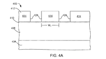
理解を容易にするため、図3は、本発明の実施形態において使用し得るプロセスの高レベルフローチャートである。パターン形成済みフォトレジストマスクが提供される(ステップ304)。図4Aは、基板404上のエッチング対象層408の概略断面図であり、エッチング対象層408上の下層410上にあるフォトレジスト特徴部414を備えたパターン形成済みフォトレジストマスク412によりスタック400が形成される。パターン形成済みフォトレジストマスク412は、線端部420において終了する一対の側壁424を有した少なくとも一本のフォトレジスト線を有する。パターン形成済みフォトレジストマスクを提供するためには、まず、エッチング対象層上にフォトレジスト層を形成し得る。その後、フォトレジスト層のパターン形成を行うことで、フォトレジスト側壁と線端部とを備えたフォトレジスト線が形成される。フォトレジスト特徴部は、図示したように幅We を有し得る。
For ease of understanding, FIG. 3 is a high-level flowchart of a process that may be used in embodiments of the present invention. A patterned photoresist mask is provided (step 304). FIG. 4A is a schematic cross-sectional view of the layer to be etched 408 on the
図4Bは、フォトレジストマスク412の上面図である。上述したように、リソグラフィ等の製造プロセスでは、プリント画像のLESが生じる。点線416は、フォトレジストマスク412に提供されたプリントパターンを示す。実際のエッチング画像は、図示したように、短縮された側壁43及び線端部436を有し得る。
FIG. 4B is a top view of the
下層410は、任意の公知の有機層、無機層、または、金属層にしてよい。限定ではなく例示を目的として、下層は、反射防止層(ARL)、裏面反射防止膜(BARC)、誘電反射防止膜(DARC)、アモルファスカーボン、SixOy、SixNy、SixOyNz 等のハードマスク、または他の任意の公知の下層にしてよい。
The
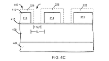
フォトレジストマスク上に被覆を配置し得る(ステップ308)。図5は、このステップの更に詳細なフローチャートである。図5に示したように、LESの低減には、ポリマ層を堆積させるステップ504とポリマ層を硬化させるステップ508とを含む循環プロセスが少なくとも一サイクル含まれる。フォトレジスト線がポリマ層により被覆された後のスタックの断面図である図4Cに示した通り、フォトレジスト特徴部412間の間隔がポリマ層の被覆前のフォトレジスト特徴部の幅「Se 」より小さい幅「Sp 」を有するように、フォトレジスト線をポリマ層により被覆または堆積させ得る。
A coating may be placed on the photoresist mask (step 308). FIG. 5 is a more detailed flowchart of this step. As shown in FIG. 5, reducing LES includes at least one cycle of a cyclic process that includes a
図4Dは、フォトレジスト線がポリマ層226により被覆された状態にある図4Cのフォトレジストマスク412の上面図である。ポリマ層226は、フォトレジスト線を被覆して、エッチング中に線端部420及び側壁424を保護し、LES比が1以下になるようにする。被覆は、LESを減少させて、フォトレジスト線の長さ及び幅を増加させる。収縮は側壁424よりも線端部420において大きな度合いで発生するため、図示したように、線端部420に堆積させるポリマの量yは、側壁424に堆積させるポリマの量xより大きくする。一実施形態において、線端部に堆積させる被覆の量は、側壁に堆積させる量の三倍程度にすることが好ましい。堆積させる被覆の量は、側壁の低減に対するLES比が1未満になるように使用し得る。
4D is a top view of the
ポリマは、炭素、水素、フッ素、またはその組み合わせを含有し得る。使用されるガスは、メタン(CH4 )等の炭化水素、フルオロカーボン、ハイドロフルオロカーボン、ヘリウム、アルゴン、またはその組み合わせにしてよい。フルオロカーボンは、化学式C4F8を有してよい。好ましくは、フルオロカーボンは、化学式CxHyFz を有する。フォトレジストマスク上にポリマを堆積させるプロセスには、約1ないし20秒が必要となり得る。 The polymer can contain carbon, hydrogen, fluorine, or a combination thereof. The gas used may be a hydrocarbon such as methane (CH 4 ), a fluorocarbon, a hydrofluorocarbon, helium, argon, or a combination thereof. The fluorocarbon may have the chemical formula C 4 F 8 . Preferably, the fluorocarbon has a chemical formula C x H y F z. The process of depositing the polymer on the photoresist mask can require about 1 to 20 seconds.
ポリマは、フルオロカーボンと臭化水素ガスとの混合物により硬化させ得る。好ましくは、フルオロカーボンは、CF4 にしてよい。循環プロセスは、所望の層が達成されるまで反復し得る。サイクルは、10回以下、好ましくは1回以上反復することが好適である。 The polymer can be cured by a mixture of fluorocarbon and hydrogen bromide gas. Preferably, the fluorocarbon may be a CF 4. The circulation process can be repeated until the desired layer is achieved. It is suitable that the cycle is repeated 10 times or less, preferably 1 time or more.
次に、図4Eに示したように、フォトレジストマスク412を介して、エッチング層408に特徴部428をエッチングし得る(ステップ316)。ポリマ被覆226の一部または全部も、このステップ中に除去されてよく、これにより、線端部及び側壁を保護して、LES比が1以下となるようにLESの量を減少させる。その後、図4Fに示したように、フォトレジストマスク412を除去する(ステップ320)。
実施例
このプロセスの例では、パターン形成済みフォトレジスト層が形成される(ステップ304)。エッチング層408、下層410、及びパターン形成済みフォトレジストマスク412を備える基板404を、エッチングチャンバ内に配置する。
Next, as shown in FIG. 4E, feature 428 may be etched into
Example In this example process, a patterned photoresist layer is formed (step 304). A
図6は、フォトレジストマスク上にポリマ層を配置し、ポリマ層を硬化させ、エッチング、及び剥離を行うために使用し得るプラズマ処理システム600の概略図である。プラズマ処理システム600は、プラズマ処理ツール601を含み得る。プラズマ処理ツール601は、誘導結合プラズマエッチングツールであり、内部にプラズマ処置チャンバ604を有するプラズマリアクタ602を含む。変圧器結合電力(TCP)コントローラ650及びバイアス電力コントローラ655は、プラズマチャンバ604内に形成されたプラズマ624に影響を与えるTCP電源651及びバイアス電源656をそれぞれ制御する。
FIG. 6 is a schematic diagram of a
TCP電力コントローラ650は、TCP整合回路652により調整された13.56MHzの高周波信号を、プラズマチャンバ604近くに位置するTCPコイル675へ供給するように構成されたTCP電源651の設定点を設定する。RF透過窓654を設けることにより、TCPコイル675からプラズマチャンバ604へのエネルギの伝達を可能にしつつ、TCPコイル675をプラズマチャンバ604から分離する。RF透過窓654の開口部に配置した約2.5cm(1インチ)の直径を有する円形のサファイア片により、光透過窓665を設けてもよい。
The
バイアス電力コントローラ655は、処理中の半導体ウェーハワーク等の基板606を受領することに適した、プラズマチャンバ604内部に位置し且つ電極608上方に直流(DC)を形成するチャック電極608に対して、バイアス整合回路657により調整されたRF信号を供給するように構成されたバイアス電源656の設定点を設定する。
The
ガス供給機構またはガスソース610は、ガスマニホルド617を介して取り付けられたガスまたはガス群のソースまたはソース群616を含み、プロセスに必要となる適切な化学物質をプラズマチャンバ604の内部へ供給する。ガス排出機構618は、圧力制御バルブ619と排気ポンプ620とを含み、プラズマチャンバ604内部から粒子を除去し、プラズマチャンバ604内において特定の圧力を維持する。
The gas supply mechanism or
温度コントローラ680は、ヒータ電源684制御することにより、チャック電極608内部に設けたヒータ682の温度を制御する。プラズマ処理システム600は、更に、電子制御回路670を含む。
The
図7A及び7Bは、本発明の実施形態において使用されるコントローラ670を実現するのに適したコンピュータシステム700を示す。図7Aは、コンピュータシステムの可能な一物理形態を示す。当然ながら、コンピュータシステムは、集積回路、プリント回路基板、及び小型携帯機器から、巨大なスーパーコンピュータに至るまで、多数の物理形態を有し得る。コンピュータシステム700は、モニタ702、ディスプレイ704、筐体706、ディスクドライブ708、キーボード710、及びマウス712を含む。ディスク714は、データをコンピュータシステム700との間で転送するために使用されるコンピュータ読み取り可能媒体である。
FIGS. 7A and 7B illustrate a
図7Bは、コンピュータシステム700のブロック図の例である。システムバス720に、様々なサブシステムが取り付けられている。プロセッサ(群)722(中央演算処理装置またはCPUとも呼ばれる)は、メモリ724を含む記憶装置に結合される。メモリ724は、ランダムアクセスメモリ(RAM)と読み出し専用メモリ(ROM)とを含む。この技術において周知であるように、ROMは、データ及び命令を一方向でCPUへ転送する機能を果たし、RAMは、通常、データ及び命令を双方向の形で転送するために使用される。こうした種類のメモリは、両方とも、以下に説明する任意の適切なコンピュータ読み取り可能な媒体を含み得る。固定ディスク726は、CPU722に双方向で結合され、追加的なデータ記憶容量を提供すると共に、同様に、以下に説明する任意のコンピュータ読み取り可能な媒体を含み得る。固定ディスク726は、プログラム、データ、及びその他を格納するのに使用し得ると共に、通常は、一次記憶装置よりも低速な(ハードディスク等の)二次記憶媒体となる。固定ディスク726内部に保持される情報は、適切である場合、標準的な形で仮想メモリとしてメモリ724に組み込み得ることは理解されよう。リムーバブルディスク714は、以下に説明する任意のコンピュータ読み取り可能な媒体の形態を取ってよい。
FIG. 7B is an example block diagram of a
CPU722は、更に、ディスプレイ704、キーボード710、マウス712、及びスピーカ730等の様々な入出力デバイスに結合される。一般に、入出力デバイスは、ビデオディスプレイ、トラックボール、マウス、キーボード、マイクロフォン、タッチ式ディスプレイ、トランスデューサカードリーダ、磁気または紙テープリーダ、タブレット、スタイラス、音声または手書き認識装置、バイオメトリクスリーダ、または他のコンピュータの何れかにしてよい。CPU722は、随意的に、ネットワークインタフェース740を使用して別のコンピュータまたは遠隔通信ネットワークに結合し得る。こうしたネットワークインタフェースにより、CPUは、上述した方法ステップを実行する過程において、ネットワークからの情報の受信またはネットワークへの情報の出力を実行し得ると考えられる。更に、本発明の方法の実施形態は、CPU722単独で実行し得るものであり、あるいは、処理の一部を共有するリモートCPUと連動して、インターネット等のネットワークを介して実行し得る。
加えて、本発明の実施形態は、更に、コンピュータにより実現される様々な動作を実行するためのコンピュータコードを有するコンピュータ読み取り可能な媒体を備えたコンピュータストレージ製品に関する。媒体及びコンピュータコードは、本発明の目的のために特別に設計及び構築されたものにしてよく、あるいは、コンピュータソフトウェア技術における当業者に周知且つ利用可能な種類のものにしてもよい。コンピュータ読み取り可能な媒体の例には、ハードディスク、フレキシブルディスク、及び磁気テープ等の磁気媒体と、CD−ROM及びホログラフィックデバイス等の光学媒体、フロプティカルディスク等の光磁気媒体、特定用途向け集積回路(ASIC)、プログラマブル論理デバイス(PLD)、及びROM及びRAMデバイス等、プログラムコードを格納及び実行するために特別に構成されたハードウェアデバイス等が含まれる。コンピュータコードの例には、コンパイラにより作成されるような機械コードと、インタプリタを使用してコンピュータにより実行される高レベルコードを含むファイルとが含まれる。コンピュータ読み取り可能な媒体は、搬送波内において実現され、プロセッサにより実行可能な一連の命令を表すコンピュータデータ信号により送信されるコンピュータコードにしてもよい。 In addition, embodiments of the present invention further relate to a computer storage product comprising a computer readable medium having computer code for performing various computer-implemented operations. The media and computer code may be specially designed and constructed for the purposes of the present invention, or may be of a type well known and available to those skilled in the computer software art. Examples of computer-readable media include magnetic media such as hard disks, flexible disks, and magnetic tape, optical media such as CD-ROMs and holographic devices, magneto-optical media such as floppy disks, and application-specific integration. Includes hardware devices that are specially configured to store and execute program code, such as circuits (ASIC), programmable logic devices (PLD), and ROM and RAM devices. Examples of computer code include machine code, such as created by a compiler, and files containing high-level code that are executed by a computer using an interpreter. The computer readable medium may be computer code that is implemented in a carrier wave and transmitted by a computer data signal representing a series of instructions that can be executed by a processor.
ポリマ層をフォトレジストマスク上に配置する(ステップ308)。図5に示したサイクルを複数回使用することでポリマ層を堆積させる(ステップ504)レシピの一例では、例えば、CH4 、C4H8、及びCxHyFz の少なくとも一つのガスを使用する。エッチングチャンバまたはプラズマ処理チャンバは、1ないし100mTの圧力を有し得る。更に好ましくは、マスクを横方向にエッチングする圧力は、2ないし8mTである。500ないし1000ワットの電力を、プラズマ処理チャンバに対して13.56MHzで供給する。温度は、約40℃ないし60℃にしてよい。レシピの一実施形態においては、20sccmのCH4 及び100sccmのHeを、温度40℃で15秒間、圧力5mT、電力500ワット、及びバイアス電力ゼロで使用する。 A polymer layer is placed on the photoresist mask (step 308). In an example of a recipe for depositing a polymer layer by using the cycle shown in FIG. 5 multiple times (step 504), for example, at least one gas of CH 4 , C 4 H 8 , and C x H y F z is used. use. The etching chamber or plasma processing chamber may have a pressure of 1 to 100 mT. More preferably, the pressure for etching the mask in the lateral direction is 2 to 8 mT. 500-1000 watts of power is supplied to the plasma processing chamber at 13.56 MHz. The temperature may be about 40 ° C to 60 ° C. In one embodiment of the recipe, 20 sccm of CH 4 and 100 sccm of He are used at a temperature of 40 ° C. for 15 seconds, a pressure of 5 mT, a power of 500 watts, and zero bias power.
プラズマ層を硬化させる(ステップ508)。ポリマ層の硬化のためのレシピの一例は、100sccmのCF4 及び25sccmのHBrといったフルオロカーボン及び臭化水素ガスを供給する。チャンバは5mTorrの圧力とする。RF電源は、周波数13.56MHz及び温度40℃において500ワットを提供する。 The plasma layer is cured (step 508). An example of a recipe for curing the polymer layer provides a fluorocarbon and hydrogen bromide gas such 100sccm of CF 4 and 25sccm of HBr. The chamber is at a pressure of 5 mTorr. The RF power supply provides 500 Watts at a frequency of 13.56 MHz and a temperature of 40 ° C.
次に、エッチング層に特徴部をエッチングする(ステップ316)。この例において、エッチング層は、ゲートを形成するためのポリシリコンである。別の実施形態において、エッチング対象層は、SiN、SiC、酸化物、金属層、または低k誘電体等、従来のエッチング層にしてよい。従来のエッチングレシピを使用して、エッチング対象層をエッチングし得る。 Next, the feature is etched into the etching layer (step 316). In this example, the etching layer is polysilicon for forming a gate. In another embodiment, the layer to be etched may be a conventional etch layer, such as SiN, SiC, oxide, metal layer, or low-k dielectric. A conventional etch recipe may be used to etch the layer to be etched.
マスクを除去するために(ステップ320)、酸素アッシングを使用し得る。 Oxygen ashing may be used to remove the mask (step 320).
本発明の好適な実施形態において、ポリマ層の配置、ポリマ層の硬化、及びエッチング層への特徴部のエッチングは、図示したような同一のエッチングチャンバ内において原位置で実行される。好ましくは、ポリマ層の配置及び硬化は、10サイクル未満に渡って実行される。更に好ましくは、ポリマ層の配置及び硬化は、少なくとも一サイクルに渡って実行される。 In a preferred embodiment of the present invention, placement of the polymer layer, curing of the polymer layer, and etching of the feature into the etch layer are performed in situ in the same etch chamber as shown. Preferably, the placement and curing of the polymer layer is performed for less than 10 cycles. More preferably, the placement and curing of the polymer layer is performed for at least one cycle.
堆積のためのレシピの一例では、チャンバ圧を25mTorrとする。堆積ガスとして100sccmのC4F8を供給する。堆積ガスは、バイアス電圧が0ボルトの状態において、500ワットのTCP電力を13.56MHzで提供することによりプラズマに転換する。堆積レシピの別の例では、CH4 レシピを使用する。この例では、チャンバ圧を5mTorrとする。堆積ガスとして20sccmのCH4 及び100sccmのHeを供給する。堆積ガスは、バイアス電圧が0ボルトの状態において、600ワットのTCP電力を13.56MHzで提供することによりプラズマに転換する。堆積ステップに続いて、HBr及びCF4 硬化ステップが行われる。 In one example of a recipe for deposition, the chamber pressure is 25 mTorr. 100 sccm of C 4 F 8 is supplied as a deposition gas. The deposition gas is converted to a plasma by providing 500 Watts of TCP power at 13.56 MHz with a bias voltage of 0 volts. Another example of a deposition recipe uses a CH 4 recipe. In this example, the chamber pressure is 5 mTorr. As a deposition gas, 20 sccm of CH 4 and 100 sccm of He are supplied. The deposition gas is converted to a plasma by providing 600 watts of TCP power at 13.56 MHz with a bias voltage of 0 volts. Following the deposition step, an HBr and CF 4 cure step is performed.
更に一般的には、堆積には、CHF3 、CH4 、CH2F2、CH4 、またはSiCl4 の少なくとも一つを含む気体化学物質が含まれ得る。 More generally, the deposition may include a gaseous chemical that includes at least one of CHF 3 , CH 4 , CH 2 F 2 , CH 4 , or SiCl 4 .
別の実施形態では、硬化ステップは使用されない。例えば、フォトレジスト及び堆積ポリマは、十分なエッチング耐性を有し、硬化ステップを必要としない。上述した、堆積ガスとして100sccmのC4F8を供給する例と、堆積ガスとして20sccmのCH4 及び100sccmのHeを供給する例とにおいて、独立した硬化ステップは省略してよい。こうしたプロセスでは、硬化ステップを排除して、こうしたプロセスの簡略化を行い、スループットを高めることが可能である。独立した硬化ステップを必要としない堆積レシピの別の例において、チャンバ圧は、5ないし10mTorrに設定される。堆積ガスとして100sccmのCF4 及び20sccmのHBrをチャンバ内に流入させる。100ないし200ボルトのバイアス電圧と共に、300ないし500ワットのTCP電力を13.56MHzで提供することにより、堆積ガスをプラズマにする。独立した硬化ステップを必要としない堆積レシピの別の例において、チャンバ圧は、5ないし10mTorrに設定される。堆積ガスとして200sccmのN2 及び20ないし50sccmのCF4 をチャンバ内に流入させる。100ないし300ボルトのバイアス電圧と共に、300ないし900ワットのTCP電力を13.56MHzで提供することにより、堆積ガスをプラズマにする。こうしたプロセスではトリミングは行われない。端から端まで堆積を行い、フォトレジストを硬化させる。 In another embodiment, no curing step is used. For example, photoresists and deposited polymers have sufficient etch resistance and do not require a curing step. In the above-described example of supplying 100 sccm of C 4 F 8 as the deposition gas and the example of supplying 20 sccm of CH 4 and 100 sccm of He as the deposition gas, independent curing steps may be omitted. In such a process, the curing step can be eliminated to simplify the process and increase throughput. In another example of a deposition recipe that does not require a separate curing step, the chamber pressure is set to 5-10 mTorr. 100 sccm of CF 4 and 20 sccm of HBr are flowed into the chamber as deposition gases. The deposition gas is made plasma by providing 300-500 watts of TCP power at 13.56 MHz with a bias voltage of 100-200 volts. In another example of a deposition recipe that does not require a separate curing step, the chamber pressure is set to 5-10 mTorr. 200 sccm of N 2 and 20-50 sccm of CF 4 are allowed to flow into the chamber as deposition gases. The deposition gas is made plasma by providing 300-900 watts of TCP power at 13.56 MHz with a bias voltage of 100-300 volts. Trimming is not performed in such a process. Deposit from end to end and cure the photoresist.
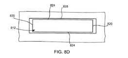
別の例は、硬化ステップを使用せず、堆積段階とトリミング段階とを有するポリマ形成プロセスを提供するプロセスである。図3のプロセスによれば、パターン形成済みフォトレジストマスクを提供する(ステップ304)。図8Aは、基板804上のエッチング対象層808の概略断面図であり、エッチング対象層808上の下層810上にあるフォトレジスト特徴部814を備えたパターン形成済みフォトレジストマスク812によりスタック800が形成される。パターン形成済みフォトレジストマスク812は、線端部において終了する一対の側壁824を有した少なくとも一本のフォトレジスト線を有する。パターン形成済みフォトレジストマスクを提供するためには、まず、エッチング対象層上にフォトレジスト層を形成し得る。その後、フォトレジスト層のパターン形成を行うことで、フォトレジスト側壁と線端部とを備えたフォトレジスト線が形成される。フォトレジスト特徴部は、図示したように幅Se を有し得る。
Another example is a process that provides a polymer forming process that does not use a curing step and has a deposition phase and a trimming phase. According to the process of FIG. 3, a patterned photoresist mask is provided (step 304). FIG. 8A is a schematic cross-sectional view of a
図4Bは、フォトレジストマスク812の上面図である。パターン形成済みフォトレジストマスク812は、線端部820において終了する一対の側壁824を有した少なくとも一本のフォトレジスト線を有する。
FIG. 4B is a top view of the
フォトレジストマスク上に被覆を配置する(ステップ308)。図9は、このステップの更に詳細なフローチャートである。図9に示したように、LES比の低減には、ポリマ層を堆積させるステップ(ステップ904)と側壁をトリミングするステップ(ステップ908)とを含む循環プロセスが少なくとも一サイクル含まれる。図8Cは、フォトレジストマスク812上にポリマ層828を堆積させた(ステップ904)後のフォトレジストマスク812の上面図である。ポリマ層828は、フォトレジスト線を被覆して、線端部820及び側壁824を保護する。この例において、側壁824に堆積させるポリマ層の厚さは、線端部820に堆積させるポリマの厚さとほぼ同じである。別の例において、厚さは、異なる関係を有し得る。こうしたプロセスのレシピの一例において、堆積の際に、チャンバ圧を5mTorrとする。堆積ガスとして20sccmのHBr、80sccmのCH4 、及び5sccmのO2 をチャンバに流入させる。堆積ガスは、バイアス電圧が0ボルトの状態において、300ないし500ワットのTCP電力を13.56MHzで提供することによりプラズマにする。図8Dは、側壁をトリミングした(ステップ908)後のフォトレジストマスク812の上面図である。
A coating is placed on the photoresist mask (step 308). FIG. 9 is a more detailed flowchart of this step. As shown in FIG. 9, reducing the LES ratio includes at least one cycle of a cyclic process that includes depositing a polymer layer (step 904) and trimming the sidewalls (step 908). FIG. 8C is a top view of the
トリミングレシピの一例では、チャンバ圧を8mTorrとする。トリミングガスとして20sccmのCl2 、20sccmのO2 、及び60sccmのHeをチャンバに流入させる。トリミングガスは、バイアス電圧が0ボルトの状態において、300ワットのTCP電力を13.56MHzで提供することによりプラズマにする。トリミングでは、側壁のポリマ、可能であれば更にフォトレジストを、線端部よりも速く選択的にエッチングし、図8Dに示したように、線端部のポリマが側壁より厚くなるようにする。図8Dの例は、ポリマのみがトリミングされた状態を示しているが、別の例においては、フォトレジストマスクの側壁の一部がトリミングされるように、側壁のポリマを完全にトリミングしてよい。その後、エッチング層に特徴部をエッチングする(ステップ316)。マスク及びポリマ層は除去される(ステップ320)。以前の実施形態と同様に、結果的に生じたポリマ層は、端部で厚くなり、側壁において薄くなるため、LESは低減される。トリミングの追加により、更に、CDの低減が可能となる。硬化ステップを有していないことから、トリミングは容易に実行される。 In an example of the trimming recipe, the chamber pressure is 8 mTorr. As a trimming gas, 20 sccm of Cl 2 , 20 sccm of O 2 , and 60 sccm of He are flowed into the chamber. The trimming gas is made into a plasma by providing 300 watts of TCP power at 13.56 MHz with a bias voltage of 0 volts. In trimming, the sidewall polymer, and possibly the photoresist, is selectively etched faster than the line ends, so that the line end polymer is thicker than the sidewalls, as shown in FIG. 8D. The example of FIG. 8D shows a state in which only the polymer is trimmed, but in another example, the sidewall polymer may be completely trimmed so that a portion of the photoresist mask sidewall is trimmed. . Thereafter, the feature is etched into the etching layer (step 316). The mask and polymer layer are removed (step 320). As in previous embodiments, the resulting polymer layer is thicker at the edges and thinner at the sidewalls, thus reducing LES. By adding trimming, it is possible to further reduce the CD. Trimming is easily performed because it does not have a curing step.
堆積及びトリミングプロセスの別の例では、少なくとも四サイクルの堆積及びその後のトリミングが実行され、各堆積において、薄層を堆積させた後、トリミングを実行して、次の堆積前に少量をトリミングする。こうした多重サイクルプロセスにより制御が向上することが分かっている。 In another example of a deposition and trimming process, at least four cycles of deposition and subsequent trimming are performed, with each deposition depositing a thin layer followed by trimming to trim a small amount before the next deposition. . It has been found that such a multi-cycle process improves control.
別の例では、堆積及びトリミングを単一ステップで実行し得るように、堆積及びトリミングを同時に実行してよい。トリミング及び堆積を単一ステップで実行するレシピの例は、次の通りである。チャンバ圧は、5mTorrに設定する。堆積及びトリミングガスとして、80ないし150sccmのCF4 、20sccmのHBr、及び0ないし5sccmのO2 を供給する。堆積及びトリミングガスは、バイアス電圧が0ボルトの状態において、300ないし625ワットを周波数13.56MHzで提供することによりプラズマにする。これは、フォトレジストを硬化させる単一の堆積及びトリミングプロセスであり、独立した硬化ステップは必要なくなる。 In another example, deposition and trimming may be performed simultaneously so that deposition and trimming can be performed in a single step. An example of a recipe that performs trimming and deposition in a single step is as follows. The chamber pressure is set to 5 mTorr. As deposition and trimming gases, 80 to 150 sccm of CF 4 , 20 sccm of HBr, and 0 to 5 sccm of O 2 are supplied. The deposition and trimming gas is made into a plasma by providing 300 to 625 watts at a frequency of 13.56 MHz with a bias voltage of 0 volts. This is a single deposition and trimming process that cures the photoresist, eliminating the need for a separate curing step.
単一ステップの堆積及びトリミングプロセスの別の例では、圧力を5mTorrとする。堆積及びトリミングガスとして、80ないし150sccmのCF4 及び20sccmのCHF3 またはCH2F2を供給する。堆積及びトリミングガスは、バイアス電圧が0ボルトの状態において、300ワットTCP電力を13.56MHzで提供することによりプラズマに転換する。このレシピは、線をトリミングするが、端から端まで堆積を行い、硬化ステップを要することなくLES比を改善する。ガスの注入及びTESCの温度は、この場合には固定されず、均一性を調整するために使用される。 In another example of a single step deposition and trimming process, the pressure is 5 mTorr. As deposition and trimming gases, 80 to 150 sccm of CF 4 and 20 sccm of CHF 3 or CH 2 F 2 are supplied. The deposition and trim gas is converted to a plasma by providing 300 Watt TCP power at 13.56 MHz with a bias voltage of 0 volts. This recipe trims the lines but deposits from end to end, improving the LES ratio without requiring a curing step. The gas injection and TESC temperature are not fixed in this case and are used to adjust the uniformity.
別の実施形態において、フォトレジストマスク上に被覆を配置すること(ステップ308)と同時に、フォトレジストマスク上にポリマを堆積させると共に、下層、例えば、BARCを単一ステップにおいてエッチングする。エッチングマスクの一部としてBARCを使用することにより、硬化ステップは回避可能となる。堆積及びBARCエッチングレシピの例において、チャンバ圧は、5ないし8mTorrに設定される。堆積及びBARCエッチングガスとして、200sccmのN2 及び20ないし50sccmのCF4 をチャンバへ流入させる。堆積及びBARCガスは、300ないし900ワットのTCP電力を13.56MHzで提供することによりプラズマにする。 In another embodiment, simultaneously with placing the coating on the photoresist mask (step 308), a polymer is deposited on the photoresist mask and the underlying layer, eg, BARC, is etched in a single step. By using BARC as part of the etching mask, the curing step can be avoided. In the example of the deposition and BARC etch recipe, the chamber pressure is set to 5-8 mTorr. As the deposition and BARC etching gas, 200 sccm N 2 and 20-50 sccm CF 4 are flowed into the chamber. The deposition and BARC gas is made into a plasma by providing 300-900 watts of TCP power at 13.56 MHz.
別の例において、BARCエッチングを提供するためのレシピでは、チャンバ圧を8mTorrとする。BARCエッチングガスとして、20sccmのCl2 、20sccmのO3 、4sccmのSiCl4 、及び60sccmのHeを供給する。BARCエッチングガスは、150ボルトまでのバイアス電圧と共に、300ないし400ワットのTCP電力を13.56MHzで提供することによりプラズマにする。別のレシピの例では、チャンバ圧を8mTorrとする。BARCエッチングガスとして、80ないし100sccmのCF4 及び20sccmのCHF3 またはCH2F2をチャンバに流入させる。BARCエッチングガスは、100ないし200ボルトのバイアス電圧と共に、300ないし400ワットのTCP電力を13.56MHzで提供することによりプラズマにする。 In another example, a recipe for providing a BARC etch has a chamber pressure of 8 mTorr. As a BARC etching gas, 20 sccm of Cl 2 , 20 sccm of O 3 , 4 sccm of SiCl 4 , and 60 sccm of He are supplied. The BARC etch gas is made into a plasma by providing 300-400 watts of TCP power at 13.56 MHz with a bias voltage up to 150 volts. In another example recipe, the chamber pressure is 8 mTorr. As the BARC etching gas, 80 to 100 sccm of CF 4 and 20 sccm of CHF 3 or CH 2 F 2 are flowed into the chamber. The BARC etch gas is turned into a plasma by providing 300-400 watts of TCP power at 13.56 MHz with a bias voltage of 100-200 volts.
以上、幾つかの好適な実施形態により本発明を説明してきたが、本発明の範囲に含まれる変更、置換、及び様々な代用等価物が存在する。更に、本発明の方法及び装置を実現する別の多数の形が存在することに留意されたい。したがって、以下の特許請求の範囲には、本発明の趣旨及び範囲に含まれる全ての変更、置換、及び様々な代用等価物が含まれると解釈されるべきである。 While the invention has been described in terms of several preferred embodiments, there are alterations, substitutions, and various substitute equivalents that fall within the scope of the invention. Furthermore, it should be noted that there are many other ways of implementing the method and apparatus of the present invention. Accordingly, the following claims should be construed to include all modifications, substitutions, and various substitute equivalents included within the spirit and scope of the present invention.
Claims (15)
線端部において終了する一対の側壁を有した少なくとも一本のフォトレジスト線を有するパターン形成済みフォトレジストマスクを、前記エッチング層上に提供するステップと、
前記少なくとも一本のフォトレジスト線の上にポリマ層を配置して、前記フォトレジスト線の前記線端部における前記ポリマ層の厚さが前記フォトレジスト線の前記側壁における前記ポリマ層の厚さより大きくするステップと、
前記フォトレジストマスクを介して前記エッチング層に特徴部をエッチングして、ラインエンドショートニング(LES)比を1以下とするステップと
を備える方法。 A method for etching a feature in an etching layer, comprising:
Providing a patterned photoresist mask on the etching layer having at least one photoresist line having a pair of sidewalls ending at a line end;
A polymer layer is disposed on the at least one photoresist line, and the thickness of the polymer layer at the line end of the photoresist line is greater than the thickness of the polymer layer at the sidewall of the photoresist line. And steps to
Etching a feature in the etching layer through the photoresist mask to have a line end shortening (LES) ratio of 1 or less.
堆積ガスを流動させるステップと、
前記堆積ガスをプラズマにするステップと、
少なくとも100ボルトの大きさのバイアス電圧を提供するステップと
を含む請求項2記載の方法。 The step of depositing the polymer layer comprises:
Flowing the deposition gas;
Turning the deposition gas into plasma;
Providing a bias voltage on the order of at least 100 volts.
ポリマを前記少なくとも一本のフォトレジスト線上に堆積させる堆積段階と、
前記少なくとも一本のフォトレジスト線の前記側壁上に堆積したポリマが、前記少なくとも一本のフォトレジスト線の前記線端部上に堆積したポリマより多くトリミングされるように、前記堆積ポリマを選択的にトリミングするトリミング段階と
を有する請求項1記載の方法。 Placing the polymer layer on the at least one photoresist line includes at least one cycle, each cycle depositing a polymer on the at least one photoresist line;
Selectively depositing the polymer so that the polymer deposited on the sidewalls of the at least one photoresist line is trimmed more than the polymer deposited on the line end of the at least one photoresist line. The method of claim 1, further comprising: a trimming step of trimming.
請求項4記載の方法。 The method of claim 4, wherein the step of placing the polymer layer over the at least one photoresist line comprises at least four cycles.
堆積ガスを流動させるステップと、
前記堆積ガスをプラズマにするステップと、
前記堆積ガスを停止するステップと、を含み、前記トリミング段階は、
トリミングガスを流動させるステップと、
前記トリミングガスをプラズマにするステップと、
前記トリミングガスを停止するステップと
を含む請求項4または請求項5に記載の方法。 The deposition step includes
Flowing the deposition gas;
Turning the deposition gas into plasma;
Stopping the deposition gas, the trimming step comprising:
Flowing the trimming gas;
Turning the trimming gas into plasma;
The method according to claim 4, further comprising a step of stopping the trimming gas.
ポリマ形成ガス及びHBrを含む堆積ガスを供給するステップと、
前記堆積ガスからプラズマを形成するステップと
を含む請求項1記載の方法。 Placing the polymer layer over the at least one photoresist line comprises:
Supplying a deposition gas comprising a polymer forming gas and HBr;
Forming a plasma from the deposition gas.
堆積ガス及びトリミングガスを同時に流動させるステップと、
前記堆積ガス及びトリミングガスをプラズマにするステップと
を含む請求項1記載の方法。 Placing the polymer layer over the at least one photoresist line comprises:
Flowing the deposition gas and the trimming gas simultaneously;
The method according to claim 1, further comprising: turning the deposition gas and the trimming gas into plasma.
CHF3 、CH4 、CH2F2、CH4 、またはSiCl4 の少なくとも一つを含む堆積ガスを供給するステップと、
前記堆積ガスをプラズマにするステップと
を含む請求項1記載の方法。 Placing the polymer layer over the at least one photoresist line comprises:
Supplying a deposition gas comprising at least one of CHF 3 , CH 4 , CH 2 F 2 , CH 4 , or SiCl 4 ;
The method of claim 1, further comprising: turning the deposition gas into plasma.
線端部において終了する一対の側壁を有した少なくとも一本のフォトレジスト線を有するパターン形成済みフォトレジストマスクを、前記エッチング層上に提供するステップと、
堆積ガスを流動させるステップ、
前記堆積ガスをプラズマに転換するステップ、及び
前記堆積ガスを停止するステップを含む
前記少なくとも一本のフォトレジスト線の上にポリマ層を配置するステップと、
トリミングガスを流動させるステップ、
前記トリミングガスをプラズマに転換するステップ、及び
前記トリミングガスを停止するステップを含む
前記ポリマ層をトリミングして、前記フォトレジスト線の前記線端部における前記トリミング済みポリマ層の厚さが前記フォトレジスト線の前記側壁における前記トリミング済みポリマ層の厚さより大きくなるようにするステップと、
前記フォトレジストマスクを介して前記エッチング層に特徴部をエッチングして、ラインエンドショートニング(LES)比を1以下とするステップと
を備える方法。 A method for etching features in an etching layer, comprising:
Providing a patterned photoresist mask on the etching layer having at least one photoresist line having a pair of sidewalls ending at a line end;
Flowing the deposition gas;
Disposing a polymer layer over the at least one photoresist line comprising: converting the deposition gas into plasma; and stopping the deposition gas;
Flowing the trimming gas;
Converting the trimming gas into plasma; and stopping the trimming gas; trimming the polymer layer, wherein the thickness of the trimmed polymer layer at the line end of the photoresist line is the photoresist. Making it greater than the thickness of the trimmed polymer layer at the sidewall of the line;
Etching a feature in the etching layer through the photoresist mask to have a line end shortening (LES) ratio of 1 or less.
Applications Claiming Priority (3)
| Application Number | Priority Date | Filing Date | Title |
|---|---|---|---|
| US11/621,902 US7491343B2 (en) | 2006-09-14 | 2007-01-10 | Line end shortening reduction during etch |
| US11/621,902 | 2007-01-10 | ||
| PCT/US2008/050524 WO2008086361A1 (en) | 2007-01-10 | 2008-01-08 | Line end shortening reduction during etch |
Related Child Applications (1)
| Application Number | Title | Priority Date | Filing Date |
|---|---|---|---|
| JP2013086806A Division JP2013191854A (en) | 2007-01-10 | 2013-04-17 | Reduction in line-end shortening during etching |
Publications (3)
| Publication Number | Publication Date |
|---|---|
| JP2010516059A JP2010516059A (en) | 2010-05-13 |
| JP2010516059A5 JP2010516059A5 (en) | 2011-02-10 |
| JP5489724B2 true JP5489724B2 (en) | 2014-05-14 |
Family
ID=39615674
Family Applications (2)
| Application Number | Title | Priority Date | Filing Date |
|---|---|---|---|
| JP2009545644A Expired - Fee Related JP5489724B2 (en) | 2007-01-10 | 2008-01-08 | Reduction of line end shortening during etching |
| JP2013086806A Pending JP2013191854A (en) | 2007-01-10 | 2013-04-17 | Reduction in line-end shortening during etching |
Family Applications After (1)
| Application Number | Title | Priority Date | Filing Date |
|---|---|---|---|
| JP2013086806A Pending JP2013191854A (en) | 2007-01-10 | 2013-04-17 | Reduction in line-end shortening during etching |
Country Status (6)
| Country | Link |
|---|---|
| US (1) | US7491343B2 (en) |
| JP (2) | JP5489724B2 (en) |
| KR (1) | KR101433987B1 (en) |
| CN (1) | CN101584027B (en) |
| TW (1) | TWI409875B (en) |
| WO (1) | WO2008086361A1 (en) |
Families Citing this family (15)
| Publication number | Priority date | Publication date | Assignee | Title |
|---|---|---|---|---|
| KR100840652B1 (en) * | 2006-12-29 | 2008-06-24 | 동부일렉트로닉스 주식회사 | Method of manufaturing cmos image sensor |
| JP2010161162A (en) | 2009-01-07 | 2010-07-22 | Tokyo Electron Ltd | Fine pattern forming method |
| KR101360876B1 (en) * | 2009-06-03 | 2014-02-11 | 어플라이드 머티어리얼스, 인코포레이티드 | Method and apparatus for etching |
| US8394723B2 (en) * | 2010-01-07 | 2013-03-12 | Lam Research Corporation | Aspect ratio adjustment of mask pattern using trimming to alter geometry of photoresist features |
| US8815747B2 (en) * | 2010-06-03 | 2014-08-26 | Micron Technology, Inc. | Methods of forming patterns on substrates |
| CN102468168B (en) * | 2010-11-01 | 2014-06-04 | 中芯国际集成电路制造(上海)有限公司 | Method for forming metal oxide semiconductor (MOS) transistor |
| US8304262B2 (en) * | 2011-02-17 | 2012-11-06 | Lam Research Corporation | Wiggling control for pseudo-hardmask |
| JP6151215B2 (en) * | 2014-05-15 | 2017-06-21 | 東京エレクトロン株式会社 | Plasma etching method |
| US10049892B2 (en) * | 2015-05-07 | 2018-08-14 | Tokyo Electron Limited | Method for processing photoresist materials and structures |
| US10049875B2 (en) * | 2016-03-04 | 2018-08-14 | Tokyo Electron Limited | Trim method for patterning during various stages of an integration scheme |
| US10157750B2 (en) * | 2016-03-28 | 2018-12-18 | Hitachi High-Technologies Corporation | Plasma processing method and plasma processing apparatus |
| US10727045B2 (en) * | 2017-09-29 | 2020-07-28 | Taiwan Semiconductor Manufacturing Company, Ltd. | Method for manufacturing a semiconductor device |
| JP2019121750A (en) * | 2018-01-11 | 2019-07-22 | 東京エレクトロン株式会社 | Etching method and etching apparatus |
| JP7195113B2 (en) | 2018-11-07 | 2022-12-23 | 東京エレクトロン株式会社 | Processing method and substrate processing apparatus |
| JP2022117597A (en) | 2021-02-01 | 2022-08-12 | 東京エレクトロン株式会社 | Temperature control method and substrate processing device |
Family Cites Families (25)
| Publication number | Priority date | Publication date | Assignee | Title |
|---|---|---|---|---|
| US5959325A (en) | 1997-08-21 | 1999-09-28 | International Business Machines Corporation | Method for forming cornered images on a substrate and photomask formed thereby |
| JP4153606B2 (en) | 1998-10-22 | 2008-09-24 | 東京エレクトロン株式会社 | Plasma etching method and plasma etching apparatus |
| KR100447263B1 (en) | 1999-12-30 | 2004-09-07 | 주식회사 하이닉스반도체 | Process for preparation of semiconductor device by using etching polymer |
| JP2001308076A (en) | 2000-04-27 | 2001-11-02 | Nec Corp | Method of manufacturing semiconductor device |
| US6451705B1 (en) | 2000-08-31 | 2002-09-17 | Micron Technology, Inc. | Self-aligned PECVD etch mask |
| US6653231B2 (en) | 2001-03-28 | 2003-11-25 | Advanced Micro Devices, Inc. | Process for reducing the critical dimensions of integrated circuit device features |
| US6553560B2 (en) | 2001-04-03 | 2003-04-22 | Numerical Technologies, Inc. | Alleviating line end shortening in transistor endcaps by extending phase shifters |
| US7125496B2 (en) | 2001-06-28 | 2006-10-24 | Hynix Semiconductor Inc. | Etching method using photoresist etch barrier |
| CN1316564C (en) * | 2002-04-11 | 2007-05-16 | 联华电子股份有限公司 | Composite photoresist layer structure |
| JP3866155B2 (en) * | 2002-05-17 | 2007-01-10 | 株式会社ルネサステクノロジ | Semiconductor device and manufacturing method thereof |
| KR100475080B1 (en) | 2002-07-09 | 2005-03-10 | 삼성전자주식회사 | Methods for forming resist pattern and fabricating semiconductor device using Si-containing water-soluble polymer |
| US6794230B2 (en) | 2002-10-31 | 2004-09-21 | Taiwan Semiconductor Manufacturing Company, Ltd. | Approach to improve line end shortening |
| TW575907B (en) | 2002-12-24 | 2004-02-11 | Macronix Int Co Ltd | Patterning method for fabricating integrated circuit |
| US6916594B2 (en) | 2002-12-30 | 2005-07-12 | Hynix Semiconductor Inc. | Overcoating composition for photoresist and method for forming photoresist pattern using the same |
| CN100423192C (en) * | 2003-03-31 | 2008-10-01 | 东京毅力科创株式会社 | Method and apparatus for multilayer photoresist dry development |
| JP4455936B2 (en) * | 2003-07-09 | 2010-04-21 | 富士通マイクロエレクトロニクス株式会社 | Semiconductor device manufacturing method and etching system |
| JP4727171B2 (en) * | 2003-09-29 | 2011-07-20 | 東京エレクトロン株式会社 | Etching method |
| CN100395874C (en) * | 2004-07-14 | 2008-06-18 | 中芯国际集成电路制造(上海)有限公司 | Manufacture method of semiconductor device for improving photo resist remainder after etch |
| KR100792409B1 (en) * | 2004-10-12 | 2008-01-09 | 주식회사 하이닉스반도체 | Method for fabrication of semiconductor device using tungsten layer to sacrificial hard mask |
| US7419771B2 (en) * | 2005-01-11 | 2008-09-02 | Taiwan Semiconductor Manufacturing Co., Ltd. | Method for forming a finely patterned resist |
| US7491647B2 (en) * | 2005-03-08 | 2009-02-17 | Lam Research Corporation | Etch with striation control |
| US7566525B2 (en) | 2005-06-14 | 2009-07-28 | Taiwan Semiconductor Manufacturing Co., Ltd. | Method for forming an anti-etching shielding layer of resist patterns in semiconductor fabrication |
| JP4652140B2 (en) * | 2005-06-21 | 2011-03-16 | 東京エレクトロン株式会社 | Plasma etching method, control program, computer storage medium |
| US7425507B2 (en) | 2005-06-28 | 2008-09-16 | Micron Technology, Inc. | Semiconductor substrates including vias of nonuniform cross section, methods of forming and associated structures |
| US7531296B2 (en) | 2005-08-24 | 2009-05-12 | Taiwan Semiconductor Manufacturing, Co., Ltd. | Method of forming high etch resistant resist patterns |
-
2007
- 2007-01-10 US US11/621,902 patent/US7491343B2/en not_active Expired - Fee Related
-
2008
- 2008-01-07 TW TW097100625A patent/TWI409875B/en not_active IP Right Cessation
- 2008-01-08 WO PCT/US2008/050524 patent/WO2008086361A1/en active Application Filing
- 2008-01-08 KR KR1020097016604A patent/KR101433987B1/en active IP Right Grant
- 2008-01-08 JP JP2009545644A patent/JP5489724B2/en not_active Expired - Fee Related
- 2008-01-08 CN CN2008800020667A patent/CN101584027B/en not_active Expired - Fee Related
-
2013
- 2013-04-17 JP JP2013086806A patent/JP2013191854A/en active Pending
Also Published As
| Publication number | Publication date |
|---|---|
| TWI409875B (en) | 2013-09-21 |
| KR101433987B1 (en) | 2014-08-25 |
| US7491343B2 (en) | 2009-02-17 |
| JP2013191854A (en) | 2013-09-26 |
| KR20090107055A (en) | 2009-10-12 |
| CN101584027A (en) | 2009-11-18 |
| CN101584027B (en) | 2011-07-13 |
| TW200845184A (en) | 2008-11-16 |
| WO2008086361A1 (en) | 2008-07-17 |
| US20080087639A1 (en) | 2008-04-17 |
| JP2010516059A (en) | 2010-05-13 |
Similar Documents
| Publication | Publication Date | Title |
|---|---|---|
| JP5489724B2 (en) | Reduction of line end shortening during etching | |
| US8329585B2 (en) | Method for reducing line width roughness with plasma pre-etch treatment on photoresist | |
| JP5086090B2 (en) | Etching method and apparatus including photoresist plasma conditioning process by hydrogen flow gradient | |
| CN100543946C (en) | Reducing of etch mask feature critical dimensions | |
| US7429533B2 (en) | Pitch reduction | |
| TWI493619B (en) | Bi-layer, tri-layer mask cd control | |
| CN101971291B (en) | Double mask self-aligned double patterning technology (sadpt) process | |
| JP5437237B2 (en) | Minimization of mask undercut in deep silicon etching | |
| US20090163035A1 (en) | Etch with high etch rate resist mask | |
| KR101690337B1 (en) | Improvement of organic line width roughness with h2 plasma treatment | |
| US20110163420A1 (en) | Aspect ratio adjustment of mask pattern using trimming to alter geometry of photoresist features | |
| TW200814142A (en) | Residue free hardmask trim | |
| CN101292197A (en) | Etch features with reduced line edge roughness | |
| TWI545648B (en) | Wiggling control for pseudo-hardmask | |
| US8986492B2 (en) | Spacer formation for array double patterning | |
| CN102318037B (en) | CD bias loading control with ARC layer open | |
| US8668805B2 (en) | Line end shortening reduction during etch |
Legal Events
| Date | Code | Title | Description |
|---|---|---|---|
| A521 | Request for written amendment filed |
Free format text: JAPANESE INTERMEDIATE CODE: A523 Effective date: 20101220 |
|
| A621 | Written request for application examination |
Free format text: JAPANESE INTERMEDIATE CODE: A621 Effective date: 20101220 |
|
| A977 | Report on retrieval |
Free format text: JAPANESE INTERMEDIATE CODE: A971007 Effective date: 20120313 |
|
| A131 | Notification of reasons for refusal |
Free format text: JAPANESE INTERMEDIATE CODE: A131 Effective date: 20120321 |
|
| A601 | Written request for extension of time |
Free format text: JAPANESE INTERMEDIATE CODE: A601 Effective date: 20120621 |
|
| A602 | Written permission of extension of time |
Free format text: JAPANESE INTERMEDIATE CODE: A602 Effective date: 20120628 |
|
| A02 | Decision of refusal |
Free format text: JAPANESE INTERMEDIATE CODE: A02 Effective date: 20121218 |
|
| A521 | Request for written amendment filed |
Free format text: JAPANESE INTERMEDIATE CODE: A821 Effective date: 20130419 |
|
| A601 | Written request for extension of time |
Free format text: JAPANESE INTERMEDIATE CODE: A601 Effective date: 20131008 |
|
| A602 | Written permission of extension of time |
Free format text: JAPANESE INTERMEDIATE CODE: A602 Effective date: 20131015 |
|
| A61 | First payment of annual fees (during grant procedure) |
Free format text: JAPANESE INTERMEDIATE CODE: A61 Effective date: 20140225 |
|
| R150 | Certificate of patent or registration of utility model |
Ref document number: 5489724 Country of ref document: JP Free format text: JAPANESE INTERMEDIATE CODE: R150 |
|
| R250 | Receipt of annual fees |
Free format text: JAPANESE INTERMEDIATE CODE: R250 |
|
| R250 | Receipt of annual fees |
Free format text: JAPANESE INTERMEDIATE CODE: R250 |
|
| R250 | Receipt of annual fees |
Free format text: JAPANESE INTERMEDIATE CODE: R250 |
|
| R250 | Receipt of annual fees |
Free format text: JAPANESE INTERMEDIATE CODE: R250 |
|
| R250 | Receipt of annual fees |
Free format text: JAPANESE INTERMEDIATE CODE: R250 |
|
| LAPS | Cancellation because of no payment of annual fees |