JP5488024B2 - AC adapter - Google Patents
AC adapter Download PDFInfo
- Publication number
- JP5488024B2 JP5488024B2 JP2010031903A JP2010031903A JP5488024B2 JP 5488024 B2 JP5488024 B2 JP 5488024B2 JP 2010031903 A JP2010031903 A JP 2010031903A JP 2010031903 A JP2010031903 A JP 2010031903A JP 5488024 B2 JP5488024 B2 JP 5488024B2
- Authority
- JP
- Japan
- Prior art keywords
- circuit board
- wiring pattern
- metal
- adapter
- connector
- Prior art date
- Legal status (The legal status is an assumption and is not a legal conclusion. Google has not performed a legal analysis and makes no representation as to the accuracy of the status listed.)
- Expired - Fee Related
Links
Images


Classifications
-
- H—ELECTRICITY
- H01—ELECTRIC ELEMENTS
- H01R—ELECTRICALLY-CONDUCTIVE CONNECTIONS; STRUCTURAL ASSOCIATIONS OF A PLURALITY OF MUTUALLY-INSULATED ELECTRICAL CONNECTING ELEMENTS; COUPLING DEVICES; CURRENT COLLECTORS
- H01R12/00—Structural associations of a plurality of mutually-insulated electrical connecting elements, specially adapted for printed circuits, e.g. printed circuit boards [PCB], flat or ribbon cables, or like generally planar structures, e.g. terminal strips, terminal blocks; Coupling devices specially adapted for printed circuits, flat or ribbon cables, or like generally planar structures; Terminals specially adapted for contact with, or insertion into, printed circuits, flat or ribbon cables, or like generally planar structures
- H01R12/50—Fixed connections
- H01R12/51—Fixed connections for rigid printed circuits or like structures
- H01R12/52—Fixed connections for rigid printed circuits or like structures connecting to other rigid printed circuits or like structures
-
- H—ELECTRICITY
- H01—ELECTRIC ELEMENTS
- H01R—ELECTRICALLY-CONDUCTIVE CONNECTIONS; STRUCTURAL ASSOCIATIONS OF A PLURALITY OF MUTUALLY-INSULATED ELECTRICAL CONNECTING ELEMENTS; COUPLING DEVICES; CURRENT COLLECTORS
- H01R12/00—Structural associations of a plurality of mutually-insulated electrical connecting elements, specially adapted for printed circuits, e.g. printed circuit boards [PCB], flat or ribbon cables, or like generally planar structures, e.g. terminal strips, terminal blocks; Coupling devices specially adapted for printed circuits, flat or ribbon cables, or like generally planar structures; Terminals specially adapted for contact with, or insertion into, printed circuits, flat or ribbon cables, or like generally planar structures
- H01R12/70—Coupling devices
- H01R12/71—Coupling devices for rigid printing circuits or like structures
- H01R12/72—Coupling devices for rigid printing circuits or like structures coupling with the edge of the rigid printed circuits or like structures
- H01R12/722—Coupling devices for rigid printing circuits or like structures coupling with the edge of the rigid printed circuits or like structures coupling devices mounted on the edge of the printed circuits
- H01R12/724—Coupling devices for rigid printing circuits or like structures coupling with the edge of the rigid printed circuits or like structures coupling devices mounted on the edge of the printed circuits containing contact members forming a right angle
Landscapes
- Coupling Device And Connection With Printed Circuit (AREA)
- Combinations Of Printed Boards (AREA)
Description
本発明は、電子部品が実装された第1の回路基板と、第1の回路基板と電気的に接続された第2の回路基板と、第2の回路基板に設けられ、第2の回路基板と電気的に接続されたコネクタと、を備えたACアダプタに関する。 The present invention provides a first circuit board on which electronic components are mounted, a second circuit board electrically connected to the first circuit board, and a second circuit board provided on the second circuit board. And an AC adapter having a connector electrically connected to the AC adapter.
電子機器(例えば、携帯型電子機器)に電源を供給するACアダプタには、ACコードを差し込むためのコネクタを備えたACアダプタがある。このような、ACアダプタでは、ACコードの抜き差しの繰り返しにより発生する応力により、ACアダプタを構成する回路基板、及び回路基板に実装された電子部品が破損する虞がある。 An AC adapter that supplies power to an electronic device (for example, a portable electronic device) includes an AC adapter that includes a connector for inserting an AC cord. In such an AC adapter, there is a possibility that the circuit board constituting the AC adapter and the electronic components mounted on the circuit board may be damaged by the stress generated by repeatedly inserting and removing the AC cord.
そこで、従来のACアダプタでは、回路基板及び電子部品の破損を防止するために、回路基板を、電子部品が実装される第1の回路基板と、コネクタが接続される第2の回路基板とに分けている(例えば、図8及び図9参照)。 Therefore, in the conventional AC adapter, in order to prevent damage to the circuit board and the electronic component, the circuit board is divided into a first circuit board on which the electronic component is mounted and a second circuit board on which the connector is connected. (See, for example, FIGS. 8 and 9).
図8は、従来のACアダプタに設けられた第1の回路基板と第2の回路基板との接続部分を拡大した平面図であり、図9は、図8に示す構造体をJ視した図である。なお、図8及び図9では、説明の便宜上、ACアダプタ200を構成する絶縁ケースの図示を省略する。
FIG. 8 is an enlarged plan view of a connection portion between a first circuit board and a second circuit board provided in a conventional AC adapter, and FIG. 9 is a view of the structure shown in FIG. It is. In FIGS. 8 and 9, the illustration of the insulating case constituting the
図8及び図9を参照するに、従来のACアダプタ200は、第1の回路基板201と、電子部品202と、第2の回路基板204と、コネクタ205と、電線207,208と、絶縁ケース(図示せず)とを有する。
8 and 9, a
第1の回路基板201は、第2の回路基板204よりも面積の大きな基板である。第1の回路基板201は、板状とされた基板本体211と、基板本体211の面211Aに設けられた配線パターン212とを有する。
The
電子部品202は、基板本体211の面211Aに実装されており、配線パターン212と電気的に接続されている。電子部品202としては、例えば、コンデンサ、トランス、スイッチング素子等を用いることができる。
The
第2の回路基板204は、板状とされた基板本体215と、基板本体215の面215Aに設けられた配線パターン217,218とを有する。
The
コネクタ205は、基板本体215の面215Bに実装されている。コネクタ205は、配線パターン217,218と電気的に接続されている。コネクタ205には、ACコードのプラグ(図示せず)が接続される側に配置されたプラグ接続面205Aを有する。コネクタ205には、ACコードに設けられたプラグ(図示せず)が繰り返し抜き差しされる。
The
電線207,208は、ワイヤが絶縁材により被覆された構成とされている。ワイヤの両端は、絶縁材から露出されている。電線207を構成するワイヤの一方の端部は、第1の回路基板201を貫通すると共に、配線パターン212と電気的に接続されている。また、電線207を構成するワイヤの他方の端部は、第2の回路基板204を貫通すると共に、配線パターン218と電気的に接続されている。
The
電線208を構成するワイヤの一方の端部は、第1の回路基板201を貫通すると共に、配線パターン212と電気的に接続されている。また、電線208を構成するワイヤの他方の端部は、第2の回路基板204を貫通すると共に、配線パターン217と電気的に接続されている。
One end of the wire constituting the
図示していない絶縁ケースは、コネクタ205のプラグ接続面205Aを露出した状態で、第1の回路基板201、電子部品202、第2の回路基板204、コネクタ205、及び電線207,208を収容するためのケースである(例えば、特許文献1参照。)。
An insulating case (not shown) accommodates the
しかしながら、従来のACアダプタ200では、ワイヤを被覆する絶縁材を備えた高価な電線207,208を用いて、第1の回路基板201と第2の回路基板204とを電気的に接続させていたため、ACアダプタ200のコストが増加してしまうという問題があった。
However, in the
また、従来のACアダプタ200では、電線207,208を、第1及び第2の回路基板201,204に接続する際、第1及び第2の回路基板201,204と電気的に接続される電線207,208の両端部を絶縁材から露出させる工程が必要であった。そのため、ACアダプタ200の製造コストが増加してしまうという問題があった。
In the
そこで、本発明は上記の点に鑑みてなされたものであり、コスト(製造コストも含む)を低減することのできるACアダプタを提供することを目的とする。 Therefore, the present invention has been made in view of the above points, and an object thereof is to provide an AC adapter capable of reducing costs (including manufacturing costs).
本発明の一観点によれば、電子部品(22)と、該電子部品(22)が実装される第1の回路基板(21)と、該第1の回路基板(21)とは分離された第2の回路基板(24)と、該第2の回路基板(24)に設けられ、前記第2の回路基板(24)と電気的に接続されたコネクタ(25)と、前記第1の回路基板(21)と前記第2の回路基板(24)とを電気的に接続する第1及び第2の電気的接続部材と、前記第1の回路基板(21)、前記電子部品(22)、前記第2の回路基板(24)、及び前記コネクタ(25)を収容すると共に、プラグ(71)が挿入される側の前記コネクタ(25)の接続面を露出させる絶縁ケース(13,14)と、を備えたACアダプタ(10)であって、前記絶縁ケース(13)は、前記第1の電気的接続部材と前記第2の電気的接続部材との間に配置され、前記第1の電気的接続部材と前記第2の電気的接続部材との間を絶縁する突出部(77)を有しており、前記第1の電気的接続部材は、第1の金属線(27)であり、前記第2の電気的接続部材は、第2の金属線(28)であることを特徴とするACアダプタ(10)が提供される。 According to one aspect of the present invention, the electronic component (22), the first circuit board (21) on which the electronic component (22) is mounted, and the first circuit board (21) are separated. A second circuit board (24), a connector (25) provided on the second circuit board (24) and electrically connected to the second circuit board (24), and the first circuit A first and second electrical connection members that electrically connect the substrate (21) and the second circuit substrate (24); the first circuit substrate (21); the electronic component (22); An insulating case (13, 14) for accommodating the second circuit board (24) and the connector (25) and exposing a connection surface of the connector (25) on the side where the plug (71) is inserted; , Wherein the insulating case (13) includes the first power supply. A protrusion (77) disposed between the electrical connection member and the second electrical connection member and insulating between the first electrical connection member and the second electrical connection member The first electrical connection member is a first metal wire (27), and the second electrical connection member is a second metal wire (28). An adapter (10) is provided.
本発明によれば、第1の電気的接続部材と第2の電気的接続部材との間に配置され、第1の電気的接続部材と第2の電気的接続部材との間を絶縁する突出部(77)を有する絶縁ケース(13,14)を設けることにより、第1及び第2の電気的接続部材を構成する導体を絶縁材で被覆する必要がなくなる。これにより、第1及び第2の電気的接続部材として、絶縁材により被覆されていない安価な第1及び第2の金属線(27,28)を用いることが可能になるため、ACアダプタ(10)のコストを低減することができる。 According to the present invention, the protrusion that is disposed between the first electrical connection member and the second electrical connection member and insulates between the first electrical connection member and the second electrical connection member. By providing the insulating case (13, 14) having the portion (77), it is not necessary to cover the conductors constituting the first and second electrical connection members with an insulating material. This makes it possible to use inexpensive first and second metal wires (27, 28) that are not covered with an insulating material as the first and second electrical connection members. ) Can be reduced.
また、第1及び第2の電気的接続部材として、絶縁材により被覆されていない第1及び第2の金属線(27,28)を用いることで、絶縁材を除去する工程が不要となるため、ACアダプタ(10)の製造コストを低減することができる。 In addition, since the first and second metal wires (27, 28) that are not covered with the insulating material are used as the first and second electrical connecting members, the step of removing the insulating material is not necessary. The manufacturing cost of the AC adapter (10) can be reduced.
また、前記第1の回路基板(21)は、前記電子部品(22)と電気的に接続された第1の配線パターン(32)を有し、前記第2の回路基板(24)は、前記コネクタ(25)と電気的に接続された第2の配線パターン(43,44)を有しており、前記第1の配線パターン(32)が形成された部分の前記第1の回路基板(21)を貫通する前記第1及び第2の金属線(27,28)の一方の端部を折り曲げ、第1の導電性ペースト(58)により、前記第1及び第2の金属線(27,28)の一方の端部を前記第1の配線パターン(32)に固定し、前記第2の配線パターン(43,44)が形成された部分の前記第2の回路基板(24)を貫通する前記第1及び第2の金属線(27,28)の他方の端部を折り曲げ、第2の導電性ペースト(45)により、前記第1及び第2の金属線(27,28)の他方の端部を前記第2の配線パターン(43,44)に固定してもよい。 The first circuit board (21) has a first wiring pattern (32) electrically connected to the electronic component (22), and the second circuit board (24) It has the 2nd wiring pattern (43,44) electrically connected with the connector (25), The said 1st circuit board (21) of the part in which the said 1st wiring pattern (32) was formed ) One end of the first and second metal wires (27, 28) penetrating through the first and second metal wires (27, 28) by bending the first conductive paste (58). ) Is fixed to the first wiring pattern (32), and passes through the second circuit board (24) in the portion where the second wiring pattern (43, 44) is formed. The other end of each of the first and second metal wires (27, 28) is bent to form a second conductive wire. The strike (45), the other end portion of the first and second metal lines (27, 28) may be fixed to the second wiring pattern (43, 44).
このように、第1の配線パターン(32)が形成された部分の第1の回路基板(21)を貫通する第1及び第2の金属線(27,28)の一方の端部を折り曲げ、第1の導電性ペースト(58)により、第1及び第2の金属線(27,28)の一方の端部を第1の配線パターン(32)に固定し、第2の配線パターン(43,44)が形成された部分の第2の回路基板(24)を貫通する第1及び第2の金属線(27,28)の他方の端部を折り曲げ、第2の導電性ペースト(45)により、第1及び第2の金属線(27,28)の他方の端部を第2の配線パターン(43,44)に固定することにより、第1及び第2の回路基板(21,24)から第1及び第2の金属線(27,28)が抜けることを防止できる。 In this way, one end of the first and second metal wires (27, 28) penetrating the first circuit board (21) in the portion where the first wiring pattern (32) is formed is bent, One end of the first and second metal lines (27, 28) is fixed to the first wiring pattern (32) by the first conductive paste (58), and the second wiring pattern (43, 44), the other end of the first and second metal wires (27, 28) penetrating the second circuit board (24) is bent, and the second conductive paste (45) is used. By fixing the other end of the first and second metal wires (27, 28) to the second wiring pattern (43, 44), the first and second circuit boards (21, 24) can be removed. The first and second metal wires (27, 28) can be prevented from coming off.
また、前記第1の金属線(27)は、前記第1の回路基板(21)に挿入される部分の前記第1の金属線(27)と前記第1の回路基板(21)に挿入されない部分の前記第1の金属線(27)との間に形成された第1の折り曲げ部(65)と、前記第2の回路基板(24)に挿入される部分の前記第1の金属線(27)と前記第2の回路基板(24)に挿入されない部分の前記第1の金属線(27)との間に形成された第2の折り曲げ部(66)と、を有し、前記第2の金属線(28)は、前記第1の回路基板(21)に挿入される部分の前記第2の金属線(28)と前記第1の回路基板(21)に挿入されない部分の前記第2の金属線(28)との間に形成された第3の折り曲げ部(65)と、前記第2の回路基板(24)に挿入される部分の前記第2の金属線(28)と前記第2の回路基板(24)に挿入されない部分の前記第2の金属線(28)との間に形成された第4の折り曲げ部(66)と、を有してもよい。 Further, the first metal line (27) is not inserted into the first metal line (27) and the first circuit board (21) in a portion to be inserted into the first circuit board (21). A first bent portion (65) formed between the portion of the first metal line (27) and a portion of the first metal wire (portion inserted into the second circuit board (24)). 27) and a second bent portion (66) formed between the portion of the first metal wire (27) not inserted into the second circuit board (24), and the second bent portion (66). The metal wire (28) of the second metal wire (28) in the portion inserted into the first circuit board (21) and the second metal wire (28) in the portion not inserted into the first circuit board (21). A third bent portion (65) formed between the second metal substrate (28) and the second circuit board (24). The fourth bent portion (66) formed between the second metal wire (28) and the second metal wire (28) at a portion not inserted into the second circuit board (24). You may have.
これにより、第1及び第2の回路基板(21,24)に挿入される第1及び第2の金属線(27,28)の長さを所定の長さにすることができる。 Thereby, the length of the 1st and 2nd metal wire (27, 28) inserted in the 1st and 2nd circuit board (21, 24) can be made into predetermined length.
さらに、前記第1及び第2の金属線(27,28)として、メッキ銅線を用いるとよい。これにより、第1及び第2の金属線(27,28)のコストを低減することができる。 Furthermore, a plated copper wire may be used as the first and second metal wires (27, 28). Thereby, the cost of the 1st and 2nd metal wires (27, 28) can be reduced.
なお、上記参照符号は、あくまでも参考であり、これによって、本願発明が図示の態様に限定されるものではない。 In addition, the said reference code is a reference to the last, and this invention is not limited to the aspect of illustration by this.
本発明によれば、ACアダプタのコスト(製造コストも含む)を低減することができる。 According to the present invention, the cost (including the manufacturing cost) of the AC adapter can be reduced.
次に、図面に基づいて本発明の実施の形態を説明する。 Next, embodiments of the present invention will be described with reference to the drawings.
(実施の形態)
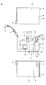
図1は、本発明の実施の形態に係るACアダプタを分解した平面図である。
(Embodiment)
FIG. 1 is an exploded plan view of an AC adapter according to an embodiment of the present invention.
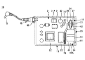
図1を参照するに、本実施の形態のACアダプタ10は、ACアダプタ本体11と、DCコード12と、絶縁ケースを構成するロアーケース13及びアッパーケース14とを有する。
Referring to FIG. 1, an
ACアダプタ本体11は、第1の回路基板21と、電子部品22と、第2の回路基板24と、コネクタ25と、第1の電気的接続部材である第1の金属線27と、第2の電気的接続部材である第2の金属線28とを有する。
The
図2は、図1に示す構造体のA−A線方向の断面図である。図2において、図1と同一構成部分には同一符号を付す。 FIG. 2 is a cross-sectional view of the structure shown in FIG. In FIG. 2, the same components as those in FIG.
図1及び図2を参照するに、第1の回路基板21は、複数の電子部品22を実装するための基板であり、基板本体31と、第1の配線パターンである配線パターン32とを有する。基板本体31は、電子部品22が実装される実装面31Aと、実装面31Aの反対側に配置され、配線パターン32が形成される面31Bと、切り欠き部34とを有する。切り欠き部34は、ロアーケース13に設けられた後述する突出部77を貫通させるためのものである。基板本体31としては、例えば、樹脂基板を用いることができる。
1 and 2, the
配線パターン32は、基板本体31の面31Bに設けられている。配線パターン32は、電子部品22と第1及び第2の金属線27,28とを電気的に接続するためのパターンである。
The
上記構成とされた第1の回路基板21は、基板本体31及び配線パターン32を貫通する2つの貫通穴(図示せず)を有する。このうち、一方の貫通穴は、第1の金属線27が挿入される穴であり、他方の貫通穴は、第2の金属線28が挿入される穴である。
The
電子部品22は、電子部品本体36と、電子部品本体36と一体的に構成されたピン端子37とを有する。電子部品本体36は、基板本体31の実装面31Aに載置されている。ピン端子37は、電子部品本体36と電気的に接続されている。ピン端子37は、基板本体31及び配線パターン32を貫通している。配線パターン32から突出した部分のピン端子37は、はんだ35により配線パターン32に固定されている。これにより、電子部品22は、配線パターン32と電気的に接続されている。電子部品22としては、例えば、コンデンサ、トランス、スイッチング素子等を用いることができる。
The
図3は、図1に示す第2の回路基板を反転させた平面図であり、図4は、図1に示すACアダプタ本体のB−B線方向の断面図である。図3及び図4において、図1と同一構成部分には同一符号を付す。なお、図4では、説明の便宜上、第1及び第2の回路基板21,24、及び第1の金属線27を断面で図示する。
3 is a plan view in which the second circuit board shown in FIG. 1 is inverted, and FIG. 4 is a cross-sectional view of the AC adapter main body shown in FIG. 3 and 4, the same components as those in FIG. In FIG. 4, for convenience of explanation, the first and
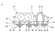
図1、図3、及び図4を参照するに、第2の回路基板24は、コネクタ25を実装するための基板であり、基板本体41と、第2の配線パターンである配線パターン43,44とを有する。基板本体41は、コネクタ25が載置されるコネクタ載置面41Aと、コネクタ載置面41Aの反対側に配置され、配線パターン43,44が形成される面41Bと、切り欠き部42とを有する。切り欠き部42は、基板本体31に設けられた切り欠き部34と対向する部分の基板本体41に形成されている。基板本体41としては、例えば、樹脂基板を用いることができる。
Referring to FIGS. 1, 3, and 4, the
配線パターン43,44は、基板本体41の面41Bに設けられている。配線パターン43は、コネクタ25と第1の金属線27とを電気的に接続している。配線パターン44は、コネクタ25と第2の金属線28とを電気的に接続している。
The
また、第2の回路基板24は、基板本体41及び配線パターン44を貫通し、第1の金属線27が挿入される貫通穴と、基板本体41及び配線パターン43を貫通し、第2の金属線28が挿入される貫通穴とを有する。
The
上記構成とされた第2の回路基板24は、第1の回路基板21よりも面方向のサイズが小さい基板である。
The
コネクタ25は、コネクタ本体51と、ピン端子53,54とを有する。コネクタ本体51は、基板本体41の面41Aに載置されている。コネクタ本体51は、ACコード(図示せず)が差し込まれる部分である。ピン端子53,54は、コネクタ本体51の下端に設けられており、コネクタ本体51と電気的に接続されている。
The
ピン端子53は、基板本体41及び配線パターン43を貫通している。ピン端子53は、はんだ56により配線パターン43に固定されている。これにより、コネクタ25は、配線パターン43と電気的に接続されている。
The
ピン端子54は、基板本体41及び配線パターン44を貫通している。ピン端子54は、はんだ56により配線パターン44に固定されている。これにより、コネクタ25は、配線パターン44と電気的に接続されている。
The
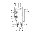
第1の金属線27は、湾曲部61と、第1の貫通部62と、第2の貫通部63と、折り曲げ部65と、折り曲げ部66とを有する。湾曲部61は、湾曲した形状とされており、基板本体31の実装面31A上に配置されている。湾曲部61は、第1及び第2の回路基板21,24に挿入されない部分である。
The
第1の貫通部62は、切り欠き部34の一方の側に位置する部分の基板本体31及び配線パターン32を貫通する貫通穴に配置されている。配線パターン32から突出した部分の第1の貫通部62は、外側に折り曲げられている。外側に折り曲げられた部分の第1の貫通部62は、第1の導電性ペーストであるはんだ58により配線パターン32に固定されている。これにより、第1の貫通部62は、配線パターン32と電気的に接続されている。
The first through
第2の貫通部63は、切り欠き部42の一方の側に位置する部分の基板本体41及び配線パターン44を貫通する貫通穴に配置されている。配線パターン44から突出した部分の第2の貫通部63は、外側に折り曲げられている。外側に折り曲げられた部分の第2の貫通部63は、第2の導電性ペーストであるはんだ58により配線パターン43に固定されている。これにより、第2の貫通部63は、配線パターン43と電気的に接続されている。
The second through
このように、配線パターン32から突出した部分の第1の貫通部62を外側に折り曲げて、はんだ58により配線パターン32に固定すると共に、配線パターン44から突出した部分の第2の貫通部63を外側に折り曲げて、はんだ45により配線パターン44に固定することにより、第1及び第2の回路基板21,24から第1の金属線27が抜けることを防止できる。
In this way, the portion of the first through
第1の折り曲げ部である折り曲げ部65は、第1の貫通部62と湾曲部61との間に配置されている。折り曲げ部65の一方の端部は、湾曲部61の一方の端部と接続されており、折り曲げ部65の他方の端部は、第1の貫通部62と接続されている。折り曲げ部65は、湾曲部61及び第1の貫通部62と一体的に構成されている。折り曲げ部65の形状は、例えば、くの字型にすることができる。
The
第2の折り曲げ部である折り曲げ部66は、第2の貫通部63と湾曲部61との間に配置されている。折り曲げ部66の一方の端部は、湾曲部61の一方の端部と接続されており、折り曲げ部66の他方の端部は、第2の貫通部63と接続されている。折り曲げ部66は、湾曲部61及び第2の貫通部63と一体的に構成されている。折り曲げ部66の形状は、例えば、くの字型にすることができる。
The
このように、第1の貫通部62と湾曲部61との間に折り曲げ部65を設けると共に、第2の貫通部63と湾曲部61との間に折り曲げ部66を設けることにより、第1及び第2の回路基板21,24に挿入される第1の金属線27の長さを所定の長さにすることができる。
As described above, the
上記構成とされた第1の金属線27の材料としては、例えば、コストの安いメッキ銅線(例えば、直径0.5mm)を用いることができる。この場合、メッキ銅線を折り曲げ加工することで第1の金属線27を形成する。
As a material of the
図5は、図1に示す構造体のC−C線方向の断面図である。図5において、図1に示す構造体と同一構成部分には同一符号を付す。 FIG. 5 is a cross-sectional view of the structure shown in FIG. 1 in the CC line direction. In FIG. 5, the same components as those of the structure shown in FIG.
図5を参照するに、第2の金属線28は、先に説明した第1の金属線27と同様な構成とされている。
Referring to FIG. 5, the
第2の金属線28を構成する第1の貫通部62は、切り欠き部34の他方の側に位置する部分の基板本体31及び配線パターン32を貫通する貫通穴に配置されている。
The first through
第2の金属線28を構成する第1の貫通部62のうち、外側に折り曲げられた部分の第1の貫通部62は、はんだ58により配線パターン32に固定されている。これにより、第2の金属線28は、配線パターン32と電気的に接続されている。
Of the first through
第2の金属線28を構成する第2の貫通部63は、切り欠き部42の他方の側に位置する部分の基板本体41及び配線パターン43を貫通する貫通穴に配置されている。
The second through
第2の金属線28を構成する第2の貫通部63のうち、外側に折り曲げられた部分の第2の貫通部63は、はんだ45により配線パターン43に固定されている。これにより、第2の金属線28は、配線パターン43と電気的に接続されている。
Of the second penetrating
なお、第2の金属線28を構成する折り曲げ部65は、第3の折り曲げ部であり、第2の金属線28を構成する折り曲げ部66は、第4の折り曲げ部である。
In addition, the bending
上記構成とされた第2の金属線28は、先に説明した第1の金属線27と同様な効果を得ることができる。第2の金属線28の材料としては、例えば、コストの安いメッキ銅線(例えば、直径0.5mm)を用いることができる。この場合、メッキ銅線を折り曲げ加工することで第2の金属線28を形成する。
The
このように、コストの安いメッキ銅線よりなる第1及び第2の金属線27,28を用いて、電子部品22が実装された第1の回路基板21と、コネクタ25が接続され、第1の回路基板21から分離された第2の回路基板24とを電気的に接続することにより、ワイヤが絶縁材により被覆された電線を用いた従来のACアダプタ200と比較して、ACアダプタ10のコストを低減することができる。
In this way, the
また、第1及び第2の金属線27,28の材料としてメッキ銅線を用いることにより、絶縁材を剥いで電線の両端に位置する部分の導体を露出させる必要がなくなるため、ACアダプタ10の製造コストを低減することができる。
Further, by using plated copper wires as the material of the first and
上記構成とされたACアダプタ本体11は、例えば、第1及び第2の回路基板21,24の母材となる1枚の回路基板を準備し、次いで、この回路基板に電子部品22及びコネクタ25を実装し、次いで、上記回路基板を切断して第1及び第2の回路基板21,24を形成し、次いで、第1及び第2の回路基板21,24の動作確認をし、次いで、第1及び第2の金属線27,28を第1及び第2の回路基板21,24に接続(具体的には、第1及び第2の金属線27,28に設けられた第1及び第2の貫通部62,63を、第1及び第2の回路基板21,24に形成された貫通穴に挿入し、その後、第1及び第2の貫通部62,63を折り曲げてはんだ45,58で固定)することで製造する。
The AC adapter
図1を参照するに、DCコード12の一方の端部は、第1の回路基板21に設けられており、第1の回路基板21に設けられた配線パターン32と電気的に接続されている。DCコード12の他方の端部には、図示していない電子機器(例えば、携帯電子機器)に装着されるプラグ71が設けられている。上記構成とされたDCコード12は、ACアダプタ本体11を製造後に、第1の回路基板21に取り付けられる。
Referring to FIG. 1, one end of the
図1を参照するに、ロアーケース13は、絶縁性を有しており、板部74と、枠部75と、突出部77,78とを有する。板部74は、板状とされており、ACアダプタ本体11を収容した際、基板本体31,41の面31B,41B(図4参照)と対向する部分である。
Referring to FIG. 1, the
枠部75は、板部74を囲むように設けられており、開口部81,82を有する。開口部81は、コネクタ25と対向する部分の枠部75に形成されている。開口部82は、DCコード12と対向する部分の枠部75に形成されている。
The
図6は、ロアーケースに収納されたACアダプタ本体を示す平面図である。図6において、図1に示す構造体と同一構成部分には、同一符号を付す。 FIG. 6 is a plan view showing the AC adapter main body housed in the lower case. In FIG. 6, the same components as those in the structure shown in FIG.
図1及び図6を参照するに、突出部77は、第1及び第2の回路基板21,24に形成された切り欠き部34,42と対向する部分の板部74に設けられている。突出部77は、板部74と一体的に構成されている。突出部77は、ロアーケース13にACアダプタ本体11を収納した際、第1及び第2の回路基板21,24に形成された切り欠き部34,42を貫通し、第1の金属線27と第2の金属線28との間に配置される仕切り板である。
Referring to FIGS. 1 and 6, the protruding
このように、第1の金属線27と第2の金属線28との間に位置する部分のロアーケース13に、絶縁性を有した突出部77を設けることにより、第1の金属線27と第2の金属線28との接触を防止することが可能となる。言い換えれば、絶縁性を有した突出部77を設けることにより、第1の回路基板21と第2の回路基板24とを電気的に接続する第1及び第2の金属線27,28として、絶縁材に被覆されていない安価なメッキ銅線を使用することができる。
Thus, by providing the
また、板部74と突出部77とを一体的に構成することにより、別途、突出部77を形成する工程を設ける必要がないため、ACアダプタ10の製造コストが増加することを防止できる。
Further, by integrally configuring the
突出部78は、第1の回路基板21と第2の回路基板24との隙間に対応する部分の板部74に設けられている。突出部78は、板部74と一体的に構成されている。突出部78は、ロアーケース13内における第1及び第2の回路基板21,24の位置を規制するための仕切り板である。
The protruding
アッパーケース14は、絶縁性を有しており、板部85と、枠部86と、開口部88,89とを有する。板部85は、板状とされており、ACアダプタ本体11を収容した際、基板本体31,41の実装面31A及びコネクタ載置面41Aと対向する部分である。
The
枠部86は、板部85を囲むように設けられている。開口部88は、コネクタ25と対向する部分の枠部86に形成されている。開口部89は、DCコード12と対向する部分の枠部86に形成されている。
The
上記構成とされたアッパーケース14は、ACアダプタ本体11が載置されたロアーケース13に装着されるケースである。
The
本実施の形態のACアダプタによれば、第1の金属線27と第2の金属線28との間に位置する部分のロアーケース13に、絶縁性を有した突出部77を設けることにより、第1の金属線27と第2の金属線28との接触を防止することが可能となる。これにより、第1の回路基板21と第2の回路基板24とを電気的に接続する第1及び第2の金属線27,28として、絶縁材に被覆されていない安価なメッキ銅線を使用することが可能となるため、ACアダプタ10のコストを低減することができる。
According to the AC adapter of the present embodiment, by providing the insulating case on the
また、板部74と突出部77とを一体的に構成することにより、別途、突出部77を形成する工程を設ける必要がないため、ACアダプタ10の製造コストが増加することを防止できる。
Further, by integrally configuring the
図7は、他のACアダプタ本体の断面図である。図7は、図4に示すACアダプタ本体11と同じ位置で他のACアダプタ本体95を切断した図である。図7において、図4に示すACアダプタ本体11と同一構成部分には、同一符号を付す。
FIG. 7 is a cross-sectional view of another AC adapter main body. FIG. 7 is a diagram in which another AC adapter
本実施の形態のACアダプタ10では、第1及び第2の金属線27,28を用いて、同一平面上に配置された第1の回路基板21と第2の回路基板24とを電気的に接続する場合を例に挙げて説明したが、図7に示すACアダプタ本体95のように、2本の金属線97(図7では、2本の金属線97を図示することが困難なため、1本の金属線97のみ図示する)を用いて、高さ方向において異なる位置に配置された第1の回路基板21と第2の回路基板24とを電気的に接続してもよい。
In the
ACアダプタ本体95は、ACアダプタ本体11に設けられた第1及び第2の金属線27,28の代わりに、2つの金属線97を設け、第1及び第2の回路基板21,24を高さ方向において異なる位置に配置した以外は、ACアダプタ本体11と同様な構成とされている。
The AC adapter
金属線97は、第1及び第2の金属線27,28に設けられた湾曲部61の代わりに、かぎ型形状とされた支持部98を設けた以外は、第1及び第2の金属線27,28と同様に構成されている。
The
ACアダプタ本体95では、基板本体31の実装面31Aを通過する平面と対向するように基板本体41のコネクタ載置面41Aが配置されている。
In the AC adapter
このような構成とされたACアダプタ本体95を備えたACアダプタは、先に説明したACアダプタ10と同様な効果を得ることができる。
The AC adapter including the AC adapter
以上、本発明の好ましい実施の形態について詳述したが、本発明はかかる特定の実施の形態に限定されるものではなく、特許請求の範囲内に記載された本発明の要旨の範囲内において、種々の変形・変更が可能である。 The preferred embodiments of the present invention have been described in detail above, but the present invention is not limited to such specific embodiments, and within the scope of the present invention described in the claims, Various modifications and changes are possible.
例えば、第1及び第2の金属線27,28に設けられた湾曲部61や第1及び第2の折り曲げ部65,66の形状は、本実施の形態で説明した形状に限定されない。
For example, the shapes of the
また、金属線97に設けられた支持部98の形状は、図7に示す形状に限定されない。
Moreover, the shape of the
本発明は、電子部品が実装された第1の回路基板と、第1の回路基板と電気的に接続された第2の回路基板と、第2の回路基板に設けられ、第2の回路基板と電気的に接続されたコネクタと、を備えたACアダプタに適用可能である。 The present invention provides a first circuit board on which electronic components are mounted, a second circuit board electrically connected to the first circuit board, and a second circuit board provided on the second circuit board. And an AC adapter provided with a connector electrically connected to each other.
10 ACアダプタ
11,95 ACアダプタ本体
12 DCコード
13 ロアーケース
14 アッパーケース
21 第1の回路基板
22 電子部品
24 第2の回路基板
25 コネクタ
27 第1の金属線
28 第2の金属線
31,41 基板本体
31A 実装面
31B,41B 面
32,43,44 配線パターン
34,42 切り欠き部
35,45,56,58 はんだ
36 電子部品本体
37 ピン端子
41A コネクタ載置面
53,54 ピン端子
61 湾曲部
62 第1の貫通部
63 第2の貫通部
65,66 折り曲げ部
71 プラグ
74,85 板部
75,86 枠部
77,78 突出部
81,82,88,89 開口部
97 金属線
98 支持部
DESCRIPTION OF
Claims (4)
前記絶縁ケースは、前記第1の電気的接続部材と前記第2の電気的接続部材との間に配置され、前記第1の電気的接続部材と前記第2の電気的接続部材との間を絶縁する突出部を有しており、
前記第1の電気的接続部材は、第1の金属線であり、
前記第2の電気的接続部材は、第2の金属線であることを特徴とするACアダプタ。 An electronic component; a first circuit board on which the electronic component is mounted; a second circuit board separated from the first circuit board; and the second circuit board. A connector electrically connected to a circuit board; first and second electrical connection members that electrically connect the first circuit board and the second circuit board; and the first circuit board. An AC adapter comprising: an insulating case that houses the electronic component, the second circuit board, and the connector, and that exposes a connection surface of the connector on a side where a plug is inserted;
The insulating case is disposed between the first electrical connection member and the second electrical connection member, and between the first electrical connection member and the second electrical connection member. Has a protruding part to insulate,
The first electrical connection member is a first metal wire;
The AC adapter, wherein the second electrical connection member is a second metal wire.
前記第2の回路基板は、前記コネクタと電気的に接続された第2の配線パターンを有しており、
前記第1の配線パターンが形成された部分の前記第1の回路基板を貫通する前記第1及び第2の金属線の一方の端部を折り曲げ、第1の導電性ペーストにより、前記第1及び第2の金属線の一方の端部を前記第1の配線パターンに固定し、
前記第2の配線パターンが形成された部分の前記第2の回路基板を貫通する前記第1及び第2の金属線の他方の端部を折り曲げ、第2の導電性ペーストにより、前記第1及び第2の金属線の他方の端部を前記第2の配線パターンに固定したことを特徴とする請求項1記載のACアダプタ。 The first circuit board has a first wiring pattern electrically connected to the electronic component,
The second circuit board has a second wiring pattern electrically connected to the connector;
One end of the first and second metal lines penetrating the first circuit board in a portion where the first wiring pattern is formed is bent, and the first and second conductive pastes are used to Fixing one end of the second metal wire to the first wiring pattern;
The other end of the first and second metal lines penetrating the second circuit board in the portion where the second wiring pattern is formed is bent, and the first and second conductive pastes are used to 2. The AC adapter according to claim 1, wherein the other end of the second metal wire is fixed to the second wiring pattern.
前記第1の金属線は、前記第1の回路基板に挿入される部分の前記第1の金属線と前記第1の回路基板に挿入されない部分の前記第1の金属線との間に形成された第1の折り曲げ部と、前記第2の回路基板に挿入される部分の前記第1の金属線と前記第2の回路基板に挿入されない部分の前記第1の金属線との間に形成された第2の折り曲げ部と、を有し、
前記第2の金属線は、前記第1の回路基板に挿入される部分の前記第2の金属線と前記第1の回路基板に挿入されない部分の前記第2の金属線との間に形成された第3の折り曲げ部と、前記第2の回路基板に挿入される部分の前記第2の金属線と前記第2の回路基板に挿入されない部分の前記第2の金属線との間に形成された第4の折り曲げ部と、を有することを特徴とする請求項1または請求項2記載のACアダプタ。 The first and second circuit boards have through holes into which the first and second metal wires are inserted,
The first metal line is formed between a portion of the first metal line inserted into the first circuit board and a portion of the first metal line not inserted into the first circuit board. Formed between the first bent portion, the first metal line of the portion inserted into the second circuit board, and the first metal line of the portion not inserted into the second circuit board. A second bent portion,
The second metal line is formed between a portion of the second metal line inserted into the first circuit board and a portion of the second metal line not inserted into the first circuit board. Formed between the third bent portion, the second metal line of the portion inserted into the second circuit board, and the second metal line of the portion not inserted into the second circuit board. The AC adapter according to claim 1, further comprising a fourth bent portion.
Priority Applications (3)
| Application Number | Priority Date | Filing Date | Title |
|---|---|---|---|
| JP2010031903A JP5488024B2 (en) | 2010-02-17 | 2010-02-17 | AC adapter |
| US13/027,634 US8467194B2 (en) | 2010-02-17 | 2011-02-15 | AC adapter |
| CN201110040026.5A CN102163908B (en) | 2010-02-17 | 2011-02-16 | AC adapter |
Applications Claiming Priority (1)
| Application Number | Priority Date | Filing Date | Title |
|---|---|---|---|
| JP2010031903A JP5488024B2 (en) | 2010-02-17 | 2010-02-17 | AC adapter |
Publications (2)
| Publication Number | Publication Date |
|---|---|
| JP2011171022A JP2011171022A (en) | 2011-09-01 |
| JP5488024B2 true JP5488024B2 (en) | 2014-05-14 |
Family
ID=44369512
Family Applications (1)
| Application Number | Title | Priority Date | Filing Date |
|---|---|---|---|
| JP2010031903A Expired - Fee Related JP5488024B2 (en) | 2010-02-17 | 2010-02-17 | AC adapter |
Country Status (3)
| Country | Link |
|---|---|
| US (1) | US8467194B2 (en) |
| JP (1) | JP5488024B2 (en) |
| CN (1) | CN102163908B (en) |
Families Citing this family (1)
| Publication number | Priority date | Publication date | Assignee | Title |
|---|---|---|---|---|
| US9554476B2 (en) * | 2014-08-14 | 2017-01-24 | Continental Automotive Systems, Inc. | Compliant staple pin for connecting multiple printed circuit boards |
Family Cites Families (30)
| Publication number | Priority date | Publication date | Assignee | Title |
|---|---|---|---|---|
| US5917707A (en) * | 1993-11-16 | 1999-06-29 | Formfactor, Inc. | Flexible contact structure with an electrically conductive shell |
| JPS62232876A (en) * | 1986-04-02 | 1987-10-13 | 松下電器産業株式会社 | Printed circuit board wiring method |
| JP2606177B2 (en) * | 1995-04-26 | 1997-04-30 | 日本電気株式会社 | Printed wiring board |
| JPH08330006A (en) * | 1995-05-30 | 1996-12-13 | Tabuchi Denki Kk | Mounting structure of connector for external connection |
| JPH10208791A (en) * | 1997-01-21 | 1998-08-07 | Canon Inc | Connection method between frame grounds inside the housing |
| US5742484A (en) * | 1997-02-18 | 1998-04-21 | Motorola, Inc. | Flexible connector for circuit boards |
| US6040624A (en) * | 1997-10-02 | 2000-03-21 | Motorola, Inc. | Semiconductor device package and method |
| JPH11167971A (en) * | 1997-12-05 | 1999-06-22 | Olympus Optical Co Ltd | Electronic apparatus |
| US6118081A (en) * | 1998-06-29 | 2000-09-12 | Motorola, Inc. | Component to substrate connection by runners and pads |
| JP2000077143A (en) * | 1998-09-01 | 2000-03-14 | Shindengen Electric Mfg Co Ltd | Ac adapter |
| US6031730A (en) * | 1998-11-17 | 2000-02-29 | Siemens Automotive Corporation | Connector for electrically connecting circuit boards |
| US6324071B2 (en) * | 1999-01-14 | 2001-11-27 | Micron Technology, Inc. | Stacked printed circuit board memory module |
| JP3032195B1 (en) * | 1999-02-10 | 2000-04-10 | 株式会社タムラ製作所 | Coil bobbin for AC adapter |
| WO2000065888A1 (en) * | 1999-04-22 | 2000-11-02 | Rohm Co., Ltd. | Circuit board, battery pack, and method of manufacturing circuit board |
| US6594152B2 (en) * | 1999-09-30 | 2003-07-15 | Intel Corporation | Board-to-board electrical coupling with conductive band |
| JP2001345133A (en) * | 2000-05-31 | 2001-12-14 | Advantest Corp | Inter-board connector structure |
| US6990355B2 (en) * | 2000-06-30 | 2006-01-24 | Sanyo Electric Co., Ltd. | Flexible printed circuit board and foldable cell phone terminal |
| JP2002133626A (en) * | 2000-10-25 | 2002-05-10 | Mitsumi Electric Co Ltd | Actuator assembly |
| FR2819111B1 (en) * | 2000-12-28 | 2003-03-07 | Thomson Csf | INTERCONNECTION MODULE FOR ELECTRICAL DEVICE HOUSING BACKGROUND |
| JP4667652B2 (en) * | 2001-06-12 | 2011-04-13 | ローム株式会社 | Battery pack and manufacturing method thereof |
| US6797891B1 (en) * | 2002-03-18 | 2004-09-28 | Applied Micro Circuits Corporation | Flexible interconnect cable with high frequency electrical transmission line |
| JP3936925B2 (en) * | 2003-06-30 | 2007-06-27 | 日本オプネクスト株式会社 | Optical transmission module |
| JP2005340385A (en) * | 2004-05-25 | 2005-12-08 | Nitto Denko Corp | Wiring circuit board and wiring circuit board connection structure |
| JP4088974B2 (en) | 2004-06-25 | 2008-05-21 | 船井電機株式会社 | AC cord connection structure |
| US6929515B1 (en) * | 2004-07-09 | 2005-08-16 | Robert Schneider | In-line AC adapter for camping and marine electrical service |
| US7304373B2 (en) * | 2004-10-28 | 2007-12-04 | Intel Corporation | Power distribution within a folded flex package method and apparatus |
| KR100659826B1 (en) * | 2005-12-20 | 2006-12-19 | 삼성에스디아이 주식회사 | Circuit board of battery pack |
| KR101106235B1 (en) * | 2006-12-07 | 2012-01-20 | 샌디스크 아이엘 엘티디 | Back-to-back pcb usb connector |
| US7388756B1 (en) * | 2006-12-12 | 2008-06-17 | The Boeing Company | Method and system for angled RF connection using a flexible substrate |
| US7618283B1 (en) * | 2008-04-23 | 2009-11-17 | Tyco Electronics Corporation | Bridge connector for connecting circuit boards |
-
2010
- 2010-02-17 JP JP2010031903A patent/JP5488024B2/en not_active Expired - Fee Related
-
2011
- 2011-02-15 US US13/027,634 patent/US8467194B2/en not_active Expired - Fee Related
- 2011-02-16 CN CN201110040026.5A patent/CN102163908B/en not_active Expired - Fee Related
Also Published As
| Publication number | Publication date |
|---|---|
| US20110199742A1 (en) | 2011-08-18 |
| JP2011171022A (en) | 2011-09-01 |
| US8467194B2 (en) | 2013-06-18 |
| CN102163908A (en) | 2011-08-24 |
| CN102163908B (en) | 2015-01-28 |
Similar Documents
| Publication | Publication Date | Title |
|---|---|---|
| JP4258432B2 (en) | Substrate bonding member and three-dimensional connection structure using the same | |
| EP2425689B1 (en) | Connecting unit | |
| KR101873950B1 (en) | Package case of electronic device | |
| US20110216512A1 (en) | Low Cost PCB Carrier and Connectivity System For Enclosed Electronics | |
| JP2020057788A (en) | Printed circuit board and motor including the same | |
| KR101425931B1 (en) | Interposer and method for manufacturing the same | |
| CN214754244U (en) | Interposer and electronic apparatus | |
| KR20100107183A (en) | Printed circuit board assembly and attaching method thereof | |
| JP3206949U (en) | Electronic equipment with plug | |
| KR100965508B1 (en) | Jumper circuit board | |
| JP5488024B2 (en) | AC adapter | |
| JP5622051B2 (en) | Board terminal and board connector using the same | |
| KR101391040B1 (en) | Printed circuit board and fabricating method thereof and electrical apparatus using the same | |
| TWM537337U (en) | Power connection device and conduction bus member | |
| JP5255592B2 (en) | substrate | |
| CN215868864U (en) | network transformer | |
| JP2020512702A (en) | Electric component, component device, and method of manufacturing component device | |
| JP5497389B2 (en) | Electrical junction box | |
| JP2019040936A (en) | Substrate assembly | |
| CN108075334B (en) | Power supply connecting device and conductive bus piece | |
| JP3161640U (en) | Universal board | |
| KR100721316B1 (en) | Connector pin for printed circuit board | |
| JP2001284756A (en) | Electronic unit | |
| CN111192736A (en) | Coil and coil packaging module | |
| JP2012160530A (en) | Board device |
Legal Events
| Date | Code | Title | Description |
|---|---|---|---|
| A621 | Written request for application examination |
Free format text: JAPANESE INTERMEDIATE CODE: A621 Effective date: 20130118 |
|
| A977 | Report on retrieval |
Free format text: JAPANESE INTERMEDIATE CODE: A971007 Effective date: 20131126 |
|
| TRDD | Decision of grant or rejection written | ||
| A01 | Written decision to grant a patent or to grant a registration (utility model) |
Free format text: JAPANESE INTERMEDIATE CODE: A01 Effective date: 20140128 |
|
| A61 | First payment of annual fees (during grant procedure) |
Free format text: JAPANESE INTERMEDIATE CODE: A61 Effective date: 20140210 |
|
| R150 | Certificate of patent or registration of utility model |
Ref document number: 5488024 Country of ref document: JP Free format text: JAPANESE INTERMEDIATE CODE: R150 |
|
| LAPS | Cancellation because of no payment of annual fees |