JP5477884B2 - Liquid crystal device and electronic device - Google Patents
Liquid crystal device and electronic device Download PDFInfo
- Publication number
- JP5477884B2 JP5477884B2 JP2008076118A JP2008076118A JP5477884B2 JP 5477884 B2 JP5477884 B2 JP 5477884B2 JP 2008076118 A JP2008076118 A JP 2008076118A JP 2008076118 A JP2008076118 A JP 2008076118A JP 5477884 B2 JP5477884 B2 JP 5477884B2
- Authority
- JP
- Japan
- Prior art keywords
- viewing angle
- angle control
- liquid crystal
- display
- pixel
- Prior art date
- Legal status (The legal status is an assumption and is not a legal conclusion. Google has not performed a legal analysis and makes no representation as to the accuracy of the status listed.)
- Expired - Fee Related
Links
Images
Landscapes
- Liquid Crystal (AREA)
Description
本発明は、広視角と狭視角の両方の表示モードを切り替え可能な液晶装置及び電子機器に関する。 The present invention relates to a liquid crystal device and an electronic apparatus capable of switching display modes of both a wide viewing angle and a narrow viewing angle.
現在、携帯電話機や携帯情報端末機、コンピュータディスプレイなどの電子機器において液晶装置が広く用いられている。このような液晶装置には、表示された画像を多くの人が様々な方向から見る場合において広い視角特性が求められ、表示された画像を周囲の人に覗かれたくない場合において狭い視角特性が求められる。 Currently, liquid crystal devices are widely used in electronic devices such as mobile phones, portable information terminals, and computer displays. Such a liquid crystal device is required to have a wide viewing angle characteristic when many people view the displayed image from various directions, and has a narrow viewing angle characteristic when the surrounding image is not desired to be viewed by surrounding people. Desired.
そこで、視角が広い表示状態と、視角が狭い表示状態とを切り替え可能な液晶装置が提案されている(例えば、特許文献1乃至5を参照)。
Accordingly, a liquid crystal device that can switch between a display state with a wide viewing angle and a display state with a narrow viewing angle has been proposed (see, for example,
特許文献1には、RGBの色画素とWの画素を1つの単位として備え、Wの画素をRGBの色画素と異なる視角特性を持たせることで、広視角表示又は狭視角表示を切り替えることが可能な垂直配向型又はツィストネマティック型の液晶表示装置が記載されている。 Japanese Patent Laid-Open No. 2004-228688 can switch between wide viewing angle display and narrow viewing angle display by providing RGB color pixels and W pixels as a single unit, and providing W pixels with different viewing angle characteristics from RGB color pixels. Possible vertical alignment or twist nematic liquid crystal display devices are described.
特許文献2乃至4には、RGBの各画素と視角制御画素とを備え、視角制御画素は上下方位或いは左右方位に液晶分子が傾くように配向制御されることで、上下左右方向に視野角調整を行うことが可能なFFS(Fringe Field Switching)方式の液晶表示装置が記載されている。かかる液晶表示装置では、視角制御画素に対して、RGBの各画素とは別個の視角制御線を介して制御電圧が印加される。これにより、上下方位或いは左右方位に液晶分子を倒すことが可能となり、視野角制御が可能となる。
特許文献5には、正面以外の方向からは表示画面とは無関係な固定パターンが見えるようにすることで、他人から覗き込みにより表示内容が盗み取られることを防止することが可能な液晶表示装置が記載されている。
ところで、一般的なFFS方式の液晶装置では、表示に寄与する表示画素は、0Vなどの基準電位が印加される共通電極と、その基準電位に対して所定の電位が印加される画素電極との間に誘電膜が形成されて構成される。そして、画素電極は一定の間隔おいて並列に配置された帯状の帯状部を有すると共に、隣り合う帯状部同士の間にはスリットが形成される。かかる液晶装置の駆動時には、画素電極の帯状部と、スリットに位置する共通電極の部分との間で電界(横電界)が生じ、この横電界により液晶分子の配向が制御される。 By the way, in a general FFS type liquid crystal device, display pixels that contribute to display include a common electrode to which a reference potential such as 0 V is applied and a pixel electrode to which a predetermined potential is applied with respect to the reference potential. A dielectric film is formed between them. The pixel electrode has strip-shaped strips arranged in parallel at regular intervals, and a slit is formed between adjacent strip-shaped portions. When such a liquid crystal device is driven, an electric field (lateral electric field) is generated between the strip portion of the pixel electrode and the common electrode portion located in the slit, and the orientation of the liquid crystal molecules is controlled by the lateral electric field.
したがって、液晶分子の配向制御を適切に行う為には、画素電極の帯状部と共通電極の部分とにおいて適切な横電界を生じさせる必要がある。そのためには、表示画素において、帯状部の幅と、隣り合う帯状部同士の間隔(=スリットの幅)との総和である帯状部の電極ピッチや、帯状部の幅と帯状部の間隔との関係を考慮した設計を行うことが重要である。 Therefore, in order to appropriately control the alignment of the liquid crystal molecules, it is necessary to generate an appropriate lateral electric field in the strip portion of the pixel electrode and the common electrode portion. For this purpose, in the display pixel, the electrode pitch of the belt-like portion, which is the sum of the width of the belt-like portion and the interval between adjacent belt-like portions (= slit width), or the width of the belt-like portion and the interval between the belt-like portions. It is important to design in consideration of the relationship.
ところが、広視角表示又は狭視角表示の両表示モードを有するFFS方式の液晶装置では、表示画素と視角制御画素との関係において、この点に関する考察が未だなされていない。即ち、上記した特許文献1乃至5では、この点に関して何らの言及がされていない。
However, in the FFS mode liquid crystal device having both the wide viewing angle display mode and the narrow viewing angle display mode, considerations regarding this point have not yet been made in relation to the display pixel and the viewing angle control pixel. That is, in the above-mentioned
本発明は、以上の点に鑑みてなされたものであり、表示画素との関係において視角制御画素における帯状部の電極ピッチ等を最適化することにより、狭視角表示モード時に、表示画面をその法線方向に対する斜め方向から見たときの画像のコントラストをより低下させることが可能な横電界方式の液晶装置及びそれを適用した電子機器を提供することを課題とする。 The present invention has been made in view of the above points, and by optimizing the electrode pitch and the like of the band-shaped portion in the viewing angle control pixel in relation to the display pixel, the display screen is displayed in the narrow viewing angle display mode. It is an object of the present invention to provide a horizontal electric field type liquid crystal device capable of further reducing the contrast of an image when viewed from an oblique direction with respect to a line direction, and an electronic apparatus to which the liquid crystal device is applied.
本発明の1つの観点では、一対の基板間に液晶層を挟持してなる液晶装置において、前記一対の基板の平面領域内には、少なくとも1つの表示画素領域と、前記一対の基板面の正面方向において暗表示を行うと共に前記一対の基板面の法線方向に対する斜め方向において当該斜め方向に応じ輝度が変化する少なくとも1つの視角制御画素領域とを有し、前記一対の基板のうち一方の基板において、前記表示画素領域は誘電体層を挟んで対向配置された一対の電極を有するとともに、前記視角制御画素領域も前記誘電体層を挟んで対向配置された一対の電極を有し、前記視角制御画素領域の前記一対の電極と前記表示画素領域の前記一対の電極とはそれぞれ独立して駆動され、前記一対の電極のうち一方の電極は、一方向に配置された複数の帯状部を有し、前記視角制御画素領域における前記帯状部のピッチは、前記表示画素領域における前記帯状部のピッチより大きく、前記視角制御画素領域において、前記一方向に隣り合う前記帯状部同士の間隔は、前記帯状部の幅と等しいか、又は前記帯状部の幅より大きい。 In one aspect of the present invention, in a liquid crystal device in which a liquid crystal layer is sandwiched between a pair of substrates, at least one display pixel region and a front surface of the pair of substrate surfaces are included in a planar region of the pair of substrates. At least one viewing angle control pixel region that performs dark display in the direction and changes in luminance according to the oblique direction in an oblique direction with respect to a normal direction of the pair of substrate surfaces, and one of the pair of substrates The display pixel region has a pair of electrodes arranged to face each other with a dielectric layer interposed therebetween, and the viewing angle control pixel region also has a pair of electrodes arranged to face each other with the dielectric layer sandwiched therebetween. The pair of electrodes in the control pixel region and the pair of electrodes in the display pixel region are driven independently, and one electrode of the pair of electrodes is a plurality of bands arranged in one direction. And the pitch of the strips in the viewing angle control pixel region is larger than the pitch of the strips in the display pixel region, and the spacing between the strips adjacent in the one direction in the viewing angle control pixel region It is greater than the width of the strip in the width and equal poetry, or the belt portion.
上記の液晶装置において、表示画素領域では一対の電極間に適宜の電圧を印加すると、表示画面を正面方向から見たときに最も透過率又は輝度の高い明表示が行われると共に、表示画面をその法線方向に対する斜め方向から見たときに極角度に応じた明表示が行われる。また、視角制御領域では一対の電極間に適宜の電圧を印加すると、表示画面を正面方向から見たときに暗表示が行われると共に、表示画面をその法線方向に対する斜め方向から見たときに極角度に応じ輝度が変化する。例えば、この場合、極角度が大きくなるに従って輝度が高くなる(明表示となる)と共にさらに極角度が大きくなるに従って輝度が低くなる(暗表示となる)。このように、視角制御画素領域の一対の電極と、表示画素領域の一対の電極とはそれぞれ独立して駆動される。 In the above liquid crystal device, when an appropriate voltage is applied between the pair of electrodes in the display pixel region, bright display with the highest transmittance or luminance is performed when the display screen is viewed from the front direction, and the display screen is When viewed from an oblique direction with respect to the normal direction, bright display according to the polar angle is performed. In addition, when an appropriate voltage is applied between the pair of electrodes in the viewing angle control region, dark display is performed when the display screen is viewed from the front direction, and when the display screen is viewed from an oblique direction with respect to the normal direction. The luminance changes according to the polar angle. For example, in this case, the luminance increases (becomes bright display) as the polar angle increases, and the luminance decreases (dark display) as the polar angle increases further. Thus, the pair of electrodes in the viewing angle control pixel region and the pair of electrodes in the display pixel region are driven independently.
このため、視角制御領域による視角制御を行わない場合、表示画素領域で形成される画像は、視角制御領域による規制はなく広視角で視認される。一方、視角制御を行う場合、表示画素領域で形成される画像は、表示画面を正面から見た場合に視角制御領域が暗表示であることから、高いコントラストが得られるために規制なく視認される。しかし、表示画面をその法線方向に対する斜め方向から見た場合は、視角制御領域において輝度が変化して画像のコントラストが低下するため、その画像を視認できなくなる。 For this reason, when viewing angle control by the viewing angle control area is not performed, an image formed in the display pixel area is not restricted by the viewing angle control area and is viewed at a wide viewing angle. On the other hand, when viewing angle control is performed, an image formed in the display pixel region is viewed without restriction because a high contrast is obtained because the viewing angle control region is dark when the display screen is viewed from the front. . However, when the display screen is viewed from an oblique direction with respect to the normal direction, the brightness changes in the viewing angle control region and the contrast of the image decreases, so that the image cannot be viewed.
特に、この液晶装置では、一対の電極のうち一方の電極は、一方向に配置された複数の帯状部を有し、視角制御画素領域における帯状部のピッチが、表示画素領域における帯状部のピッチより大きい。ここで、前記一方の電極は、梯子状の平面形状を有することが好ましい。また、前記帯状部のピッチは、前記一方向における前記帯状部の幅と、前記一方向に隣り合う前記帯状部同士の間隔との総和に等しい。これにより、狭視角表示モード時に、例えば表示画面をその法線方向に対する斜め方向から見たときの輝度を変化させて、当該斜め方向における画像のコントラストをさらに低下させることができる。したがって、当該斜め方向から見た画像をより判別し難くすることができ、良好な狭視角表示効果が得られる。 In particular, in this liquid crystal device, one of the pair of electrodes has a plurality of strips arranged in one direction, and the pitch of the strips in the viewing angle control pixel region is the pitch of the strips in the display pixel region. Greater than. Here, it is preferable that the one electrode has a ladder-like planar shape. In addition, the pitch of the belt-like portions is equal to the sum of the width of the belt-like portions in the one direction and the interval between the belt-like portions adjacent in the one direction. Accordingly, in the narrow viewing angle display mode, for example, the luminance when the display screen is viewed from an oblique direction with respect to the normal direction can be changed, and the contrast of the image in the oblique direction can be further reduced. Therefore, the image viewed from the oblique direction can be made more difficult to distinguish, and a good narrow viewing angle display effect can be obtained.
他の好適な例では、前記視角制御画素領域における前記帯状部のピッチは10〜30[μm]であり、前記表示画素領域における前記帯状部のピッチは2〜8[μm]であることが好ましい。また、前記視角制御画素領域における該視角制御画素領域の透過率のピークは、前記帯状部のピッチが15〜25[μm]の間に存在している。また、前記一対の基板面の法線方向の方位角を0[°]とした場合に、前記視角制御画素領域の透過率のピークは、前記法線方向から前記一対の基板面に対して40[°]〜60[°]の方位に存在している。これらにより、表示画素領域の前記帯状部のピッチとの関係において、狭視角表示モードを実現するための最適な視角制御領域の前記帯状部のピッチを設定することが可能となる。 In another preferred example, the pitch of the band-like portions in the viewing angle control pixel region is preferably 10 to 30 [μm], and the pitch of the band-like portions in the display pixel region is preferably 2 to 8 [μm]. . Moreover, the peak of the transmittance of the viewing angle control pixel region in the viewing angle control pixel region exists when the pitch of the band-shaped portion is 15 to 25 [μm]. Further, when the azimuth angle in the normal direction of the pair of substrate surfaces is set to 0 [°], the transmittance peak of the viewing angle control pixel region is 40 with respect to the pair of substrate surfaces from the normal direction. It exists in the direction of [°] to 60 [°]. Accordingly, it is possible to set the optimum pitch of the band-like portion of the viewing angle control region for realizing the narrow viewing angle display mode in relation to the pitch of the belt-like portion of the display pixel region.
また、本開示では、前記視角制御画素領域において、前記一方向に隣り合う前記帯状部同士の間隔を、前記帯状部の幅と等しくするか、又は前記帯状部の幅より大きくすることにより、良好な狭視角表示効果が得られる。
Further, in the present disclosure, in the viewing angle control pixel region, the spacing of the strip portions adjacent to each other in the one direction, or the like properly and width of the strip portion, or by greater than the width of said strip portion, Good narrow viewing angle display effect can be obtained.
上記の液晶装置の一つの態様では、前記視角制御画素領域において前記一対の電極間に発生する電界の方向は、前記液晶層を構成する液晶分子の初期配向方向に対して交差する方向であって且つ前記一対の基板面の法線方向に沿っている。この態様では、視角制御領域において一対の電極間に電圧を印加すると、液晶分子が一対の基板面の法線方向に配向するため、表示画面を正面方向から見たときに暗表示が行われると共に、表示画面をその法線方向に対する斜め方向から見たときに極角度に応じ輝度が変化する。 In one aspect of the liquid crystal device, the direction of the electric field generated between the pair of electrodes in the viewing angle control pixel region is a direction that intersects an initial alignment direction of liquid crystal molecules that form the liquid crystal layer. And it is along the normal line direction of said pair of substrate surface. In this aspect, when a voltage is applied between the pair of electrodes in the viewing angle control region, the liquid crystal molecules are aligned in the normal direction of the pair of substrate surfaces, so that dark display is performed when the display screen is viewed from the front direction. When the display screen is viewed from an oblique direction with respect to the normal direction, the luminance changes according to the polar angle.
本発明の他の観点では、上記の液晶装置を表示部として備える電子機器を構成することができる。この構成によれば、例えば、広視角及び狭視角の両表示モードを有し、狭視角表示モード時に、表示画面をその法線方向に対する斜め方向から見たときの映像のコントラストを低下させることが可能な電子機器を構成することができる。 In another aspect of the present invention, an electronic device including the above-described liquid crystal device as a display portion can be configured. According to this configuration, for example, both the wide viewing angle and the narrow viewing angle display modes are provided, and in the narrow viewing angle display mode, the contrast of the image when the display screen is viewed from an oblique direction with respect to the normal direction can be reduced. Possible electronic devices can be configured.
以下、図面を参照して本発明を実施するための最良の形態について説明する。 The best mode for carrying out the present invention will be described below with reference to the drawings.
[液晶装置の構成]
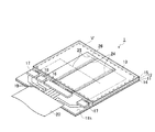
まず、図1を参照して、本発明の実施形態に係る液晶装置1の概略構成について説明する。図1は、本実施形態に係る液晶装置1の概略構成を示す斜視図である。なお、図1では、便宜上、視角制御線26を実線で示している。
[Configuration of liquid crystal device]
First, a schematic configuration of a
この液晶装置1は、横電界方式の一例としてのFFS(Fringe−Field Switching)方式の液晶装置である。液晶装置1は、表示画素をスイッチング制御するTFT(Thin Film Transistor)素子を有する素子基板11と対向基板12とを枠状のシール材(図示略)を介して貼り合わせ、素子基板11と対向基板12との間のシール材で区画される領域内に、例えば正の誘電率異方性を有するネマチック型の液晶層13を狭持して構成される。液晶装置1におけるシール材の内側には、画像を表示するための画像表示領域(一点鎖線にて囲まれる領域)Vが形成されている。
The
素子基板11は、対向基板12の一端から外側に張り出す張り出し領域11hを有する。張り出し領域11hの対向基板12側の面上には、データ線駆動回路16、走査線駆動回路17、視角制御線駆動回路18、複数の外部接続用配線19、及びFPC(Flexible Printed Circuits)20が夫々形成又は実装されている。データ線駆動回路16、走査線駆動回路17及び視角制御線駆動回路18は、各外部接続用配線19を介してFPC20に電気的に接続されている。素子基板11の液晶層13側とは逆側には第1偏光板14が配置されていると共に、対向基板12の液晶層13側とは逆側には第2偏光板15が配置されている。第1偏光板14の素子基板11側とは逆側には、照明装置としてのバックライト(図示略)が配置される。
The
次に、図2を参照して、本実施形態に係る液晶装置1の電気的な構成について説明する。図2は、液晶装置1の電気的な構成を示す等価回路図である。
Next, an electrical configuration of the
液晶装置1の画像表示領域Vには、複数の表示画素(表示画素領域)Pa及び視角制御画素(視角制御画素領域)Pbがマトリックス状に配置されていると共に、複数のデータ線24、複数の視角制御線26及び複数の走査線25が格子状に配置されている。
In the image display area V of the
表示画素Paは、それぞれ異なる色、例えばR(赤)、G(緑)、B(青)の各色の光を出力する3つのサブ表示画素(サブ表示画素領域)Pcを有している。表示画素Paを構成する3つのサブ表示画素Pc、即ちR、G、Bの各サブ表示画素Pcは、一方向(本例では走査線25の延在方向)に沿ってこの順に配置されている。但し、本発明では、R、G、Bの各色のサブ表示画素Pcの配列順序に限定はない。各サブ表示画素Pcは、画素電極21と、画素電極21をスイッチング制御するためのTFT素子23と、を備えて構成される。TFT素子23は、ソース電極23sと、ゲート電極23gと、ドレイン電極23dと、を備えている。ソース電極23sは、データ線24と電気的に接続されている。ゲート電極23gは、走査線25と電気的に接続されている。ドレイン電極23dは画素電極21と電気的に接続されている。
The display pixel Pa has three sub display pixels (sub display pixel regions) Pc that output light of different colors, for example, R (red), G (green), and B (blue). The three sub display pixels Pc constituting the display pixel Pa, that is, the sub display pixels Pc of R, G, and B, are arranged in this order along one direction (in this example, the extending direction of the scanning line 25). . However, in the present invention, there is no limitation on the arrangement order of the sub-display pixels Pc of R, G, and B colors. Each sub display pixel Pc includes a
視角制御画素Pbは、複数の表示画素Paの各々に対応して配置されている。本例では、各視角制御画素Pbは、任意の1つの表示画素Paを構成するBのサブ表示画素と、当該任意の1つの表示画素Paに対し走査線25の延在方向に隣接する位置に設けられた他の1つの表示画素Paを構成するRのサブ表示画素Pcとの間に対応して配置されている。視角制御画素Pbは、画素電極22を備えるが、TFT素子23を備えていない。視角制御画素Pbは、後述する視角制御線駆動回路18及び視角制御線26を通じて、サブ表示画素Pcとは独立して駆動される。
The viewing angle control pixel Pb is arranged corresponding to each of the plurality of display pixels Pa. In this example, each viewing angle control pixel Pb is located at a position adjacent to the B sub-display pixel constituting one arbitrary display pixel Pa and the extending direction of the
各データ線24は、データ線駆動回路16より供給される画像信号S1〜Snをサブ表示画素Pcに供給する。走査線25は、走査線駆動回路17より供給される走査信号G1〜Gmをサブ表示画素Pcに供給する。
Each
視角制御線26は、櫛歯状の形状を有し、複数の櫛歯部分26aを有する。各櫛歯部分26aは、データ線24の延在方向に列をなす各視角制御画素Pbに直接的且つ電気的に接続される。また、視角制御線26は、視角制御線駆動回路18に電気的に接続されている。
The viewing
視角制御線駆動回路18は、データ線駆動回路16及び走査線駆動回路17とは独立して、狭視角表示モード時に視角制御線26に視角制御用信号Kを供給する一方、広視角表示モード時に視角制御線26に視角制御用信号(例えばOFF信号)Kを供給する、言い換えれば視角制御用信号Kの供給を停止する。好適な例では、視角制御線駆動回路18は、例えば、電気信号をスイッチング(ON/OFF)することが可能なトランジスタなどのスイッチング素子を含んで構成される。この場合、視角制御線駆動回路18は、スイッチング素子をON/OFFさせることにより、視角制御線26に対し視角制御用信号(ON/OFF信号)Kを供給することができる。なお、本実施形態では、画素電極22を駆動するための視角制御線駆動回路18を液晶装置1に設けているが、これに限らず、本発明では、視角制御線駆動回路18を、FPC20や後述する電子機器に設けることとしても構わない。
The viewing angle control
次に、図3及び図4を参照して、液晶装置1の詳細な構成について説明する。
Next, a detailed configuration of the
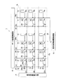
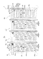
図3は、3つのサブ表示画素Pcから構成される任意の1つの表示画素Pa及び当該1つの表示画素Paに対応して配置される1つの視角制御画素Pbを含む液晶装置1の構成を示す平面図である。図4は、図3の切断線A−A’に沿った液晶装置1の要部断面図を示す。
FIG. 3 shows a configuration of the
まず、素子基板11の構成は次の通りである。
First, the configuration of the
素子基板11は、例えばガラスや石英、プラスチックなどの透光性材料からなる基板本体31と、基板本体31の液晶層13側の面から液晶層13側に向けて順次積層されたゲート絶縁膜32、第1層間絶縁膜33、誘電体層としての第2層間絶縁膜34及び配向膜35と、を備えている。また、素子基板11は、基板本体31の液晶層13側の面上に形成された走査線25と、ゲート絶縁膜32の液晶層13側の面上に形成されたデータ線24、視角制御線26(図示略)、半導体層36、ソース電極37及びドレイン電極38と、第1層間絶縁膜33の液晶層13側の面上に形成された共通電極39と、第2層間絶縁膜34の液晶層13側の面上に形成された画素電極21及び画素電極22(図示略)と、を備えている。
The
ゲート絶縁膜32は、例えばSiO2(酸化シリコン)などの透光性材料により形成されており、基板本体31上に形成された走査線25を覆っている。第1層間絶縁膜33は、例えばSiN(窒化シリコン)などの透光性材料により形成されており、ゲート絶縁膜32と、ゲート絶縁膜32上に形成されたデータ線24、視角制御線26(図示略)、半導体層36、ソース電極37及びドレイン電極38とを覆っている。第2層間絶縁膜34は、例えば感光性を有するアクリル樹脂などの透光性材料により形成されており、第1層間絶縁膜33と、第1層間絶縁膜33上に形成された共通電極39とを覆っている。配向膜35は、例えばポイリミド樹脂などの透光性材料により形成されており、第2層間絶縁膜34と、第2層間絶縁膜34上に形成された画素電極21及び画素電極22(図示略)とを覆っている。配向膜35の液晶層13側の面には、液晶層13を構成する液晶分子13aの初期配向方向を所定の方向(本例ではデータ線24の延在方向)に規定する配向処理が施されている。
The
走査線25は、図3に示すように、平面視するとサブ表示画素Pc及び視角制御画素Pbの各短軸方向に沿って配置されている。そして、走査線25は、図3及び図4に示すように、ゲート絶縁膜32を介して半導体層36のチャンネル領域と重なっている。データ線24は、図3に示すように、平面視するとサブ表示画素Pcの長軸方向に沿って配置されている。視角制御線26は、図3に示すように、平面視すると視角制御画素Pbの長軸方向に沿って配置されている。
As shown in FIG. 3, the
半導体層36は、図3及び図4に示すように、アモルファスシリコンなどの半導体により形成されており、不純物を注入しないことで形成されたチャンネル領域と不純物を注入することで形成されたソース領域及びドレイン領域とを有している。
As shown in FIGS. 3 and 4, the
ソース電極37は、データ線24から分岐して形成されており、半導体層36のソース領域に電気的に接続されている。ドレイン電極38は、半導体層36のドレイン領域に電気的に接続されており、第1層間絶縁膜33及び第2層間絶縁膜34を貫通するコンタクトホールH1を介して画素電極21に電気的に接続されている。
The
共通電極39は、例えばITO(酸化インジウムスズ)などの透光性導電材料により形成されており、第1層間絶縁膜33を覆っている。そして、共通電極39は、コンタクトホールH1に対応する位置に設けられ、当該共通電極39と画素電極21、22及びドレイン電極38との絶縁を図るための開口39aを備える。また、共通電極39には、例えば液晶層13の駆動に用いられる所定の基準電圧(例えば、所定の一定の電圧或いは0V、または所定の一定の電位とこれと異なる他の所定の一定の電位とが周期的(フレーム期間毎又はフィールド期間毎)に切り替わる信号)が印加される。
The
画素電極21は、共通電極39と同様に、例えばITOなどの透光性導電材料により形成されている。画素電極21は、図3及び図4に示すように、サブ表示画素Pcにおける第2層間絶縁膜34上に形成されており、略梯子状の平面形状を有する。画素電極21は、図3及び図4に示すように、一対の本線部21aと、複数の帯状部21bと、を備えている。一対の本線部21aの各々は、サブ表示画素Pcの長軸方向の端部に配置されていると共に、走査線25の延在方向と略平行な方向に延在している。また、一対の本線部21aのうち走査線25に近接して配置された一方の本線部21aは、コンタクトホールH1を介してTFT素子23のドレイン電極38に電気的に接続されている。
Similar to the
各帯状部21bは、帯状の平面形状を有し、サブ表示画素Pcの長軸方向(又はデータ線24の延在方向)に対し所定の傾斜角度を以って延在している。また、各帯状部21bは、サブ表示画素Pcの短軸方向(言い換えれば、走査線25の延在方向)に一定の間隔をおいて並列に配置されていると共に、相互に略平行をなすように配置されている。このため、各サブ表示画素Pcの短軸方向に隣り合う帯状部21bの間にはスリット(開口)21sが形成されている。各帯状部21bの両端は、一対の本線部21aの各々に電気的に接続されている。なお、複数の帯状部21bのうち、サブ表示画素Pcの短軸方向の端部に配置されている一部の帯状部21bは、一対の本線部21aのうち何れか一方の本線部21aにのみ電気的に接続されている。
Each belt-
画素電極22は、共通電極39と同様に、例えばITOなどの透光性導電材料により形成されている。画素電極22は、図3及び図4に示すように、視角制御画素Pbにおける第2層間絶縁膜34上に形成されており、略梯子状の平面形状を有する。画素電極22は、略矩形枠状の平面形状を有する枠状部22aと、枠状部22aの内側に配置された複数の帯状部22bとを有する。枠状部22aは、第1層間絶縁膜33及び第2層間絶縁膜34を貫通するコンタクトホールH1を介して視角制御線26の櫛歯部分26aから分岐する分岐部26abに電気的に接続されている。各帯状部22bは、帯状の平面形状を有し、視角制御画素Pbの短軸方向に沿って相互に略平行となるように延在している。また、各帯状部22bは、視角制御画素Pbの長軸方向(言い換えれば、データ線24又は視角制御線26の櫛歯部分26aの延在方向)に一定の間隔をおいて並列に配置されている。このため、各視角制御画素Pbの長軸方向に隣り合う帯状部22bの間にはスリット(開口)22sが形成されている。各帯状部22bの両端は、視角制御画素Pbの長軸方向に沿って延在する枠状部22aの部分に電気的に接続されている。
Similarly to the
以上より、この液晶装置1では、帯状部21b、22bと共通電極39との間に電圧を印加することにより、画素電極21、22と共通電極39との間に電界(横電界)が生じ、これにより液晶分子13aを駆動する。このように、この液晶装置1では、画素電極21と共通電極39と、及び画素電極22と共通電極39とは、それぞれFFS方式の電極構造を構成している。
As described above, in this
次に、対向基板12の構成は次の通りである。
Next, the configuration of the
対向基板12は、図4に示すように、基板本体31と同様の素材よりなる基板本体41と、基板本体41の液晶層13側の面から液晶層13側に順次積層された遮光膜42、カラーフィルタ層43及び配向膜44と、を備えている。
As shown in FIG. 4, the
遮光膜42は、遮光性を有する素材にて形成され、基板本体41の液晶層13側の面上において、各サブ表示画素Pcを区画する位置及び各視角制御画素Pbを区画する位置にそれぞれ配置されている。カラーフィルタ層43は、R、G、Bの各色のカラーフィルタ層を含み、各サブ表示画素Pcに対応して配置されている。但し、カラーフィルタ層43は、各視角制御画素Pbに対応する領域には設けられていない。配向膜44は、図4に示すように、配向膜35と同様に、例えばポイリミド樹脂などの透光性材料により形成されている。配向膜44の液晶層13側の面には、液晶分子13aの初期配向方向を所定の方向(本例ではデータ線24の延在方向)であって配向膜35と反平行な方向とする配向処理が施されている。
The
[液晶装置の動作]
次に、図5(a)及び(b)を参照して、液晶装置1の動作について説明する。
[Operation of liquid crystal device]
Next, the operation of the
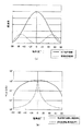
図5(a)は、サブ表示画素Pc及び視角制御画素Pbに一定の電圧を印加した時の、サブ表示画素Pc及び視角制御画素Pbの透過率(又は輝度)の視角特性の一例を示すグラフである。図5(a)において、縦軸は透過率を示し、横軸は液晶装置1の表示面の法線方向(正面方向)の方位を0[°]としたときに、その法線方向からデータ線24の延在方向と略直交する方向又は第2偏光板15の吸収軸方向に±θずらした極角度[°]を示す。なお、図5(a)において、縦軸に示す透過率は図中の上側に向かうに連れて高くなる。図5(b)は、視角制御画素Pbの駆動時及び非駆動時におけるコントラストの視角特性の一例を示すグラフである。図5(b)において、縦軸はコントラストを示し、横軸は図5(a)と同様の極角度[°]を示す。
FIG. 5A is a graph showing an example of viewing angle characteristics of transmittance (or luminance) of the sub display pixel Pc and the viewing angle control pixel Pb when a constant voltage is applied to the sub display pixel Pc and the viewing angle control pixel Pb. It is. In FIG. 5A, the vertical axis indicates the transmittance, and the horizontal axis indicates data from the normal direction when the orientation of the normal direction (front direction) of the display surface of the
バックライトから照射された光は、第1偏光板14により直線偏光に変換されて液晶層13に入射する。ここで、サブ表示画素Pcにおいて画素電極21と共通電極39との間に電圧を印加しない非駆動時の場合、液晶層13に入射した直線偏光は、液晶層13により入射時と同一の偏向状態で液晶層13から出射する。この直線偏光は、その偏向方向が第2偏光板15の吸収軸と平行であるため第2偏光板15で遮断される。したがって、サブ表示画素Pcでは、非駆動時において暗表示が行われる。なお、サブ表示画素Pcは、正面から見たときも斜め方向から見たときも暗表示となる。
The light emitted from the backlight is converted into linearly polarized light by the first
また、サブ表示画素Pcにおいて画素電極21と共通電極39との間に電圧を印加する駆動時の場合、画素電極21の長軸方向と略平行な方向に沿って初期配向状態にある液晶分子13aは、図3に示す矢印A1のように、素子基板11及び対向基板12の各基板面上で回転して画素電極21の長軸方向と交差(本例では略直交)する方向に再配向する。これにより、液晶層13に入射した直線偏光は、液晶層13により所定の位相差が付与され、入射時の偏向方向と直交する直線偏光に変換されて液晶層13より出射し、さらに第2偏光板15を透過する。したがって、サブ表示画素Pcでは、駆動時において表示光として視認される明表示が行われる。ここで、サブ表示画素Pcでは、図5(a)に示すように、正面から見たときに最も透過率(又は輝度)が高くなり、斜め方向から見たときにその極角度が大きくなるに従って透過率(又は輝度)が低くなる。
Further, in the case of driving in which a voltage is applied between the
一方、視角制御画素Pbにおいて画素電極22と共通電極39との間に電圧を印加しない非駆動時の場合、上述と同様に、視角制御画素Pbでは暗表示が行われる。なお、視角制御画素Pbは、正面から見たときも斜め方向(液晶装置1の表示面の法線方向に対する斜め方向)から見たときも暗表示となる。
On the other hand, in the non-driving state where no voltage is applied between the
また、視角制御画素Pbにおいて画素電極22と共通電極39との間に電圧を印加する駆動時の場合、帯状部22bの延在方向と交差(本例では略直交)する方向に沿って初期配向状態にある液晶分子13aは、図3に示す矢印A2のように、素子基板11及び対向基板12の各基板面に対して垂直方向(法線方向)に再配向する。ここで、視角制御画素Pbは、図5(a)に示すように、液晶層13における位相差変化がないため、正面から見たときに暗表示となる。また、視角制御画素Pbは、第2偏光板15の吸収軸方向における斜め方向(液晶装置1の表示面の法線方向に対する斜め方向)から見たときに、液晶層13における位相差変化に応じてその極角度に応じ輝度(又は透過率)が変化、即ち、その極角度が大きくなるに従って輝度が高くなる(明表示となる)と共にさらに極角度が大きくなるに従って輝度が低くなる(暗表示となる)。本例における視角制御画素Pbでは、透過率のピークが極角度+40[°]〜+60[°]及び極角度−40[°]〜−60[°]の各範囲内に存在している。
Further, in the case of driving in which a voltage is applied between the
以上のように、本実施形態では、視角制御画素Pbの駆動及び非駆動によって視角特性を変えることができる。即ち、視角制御画素Pbが非駆動時の場合、各サブ表示画素Pcを適宜、駆動又は非駆動させることにより画像表示領域Vに形成された画像は、正面から見たときも斜め方向から見たときも視認される。なお、視角制御画素Pbを非駆動としたときのコントラストは、図5(b)に示すように、正面から見たときに最も高くなり、斜め方向から見たときにその極角度が大きくなるに従って低くなる。本例では、視角制御画素Pbを非駆動とした場合には、極角度−80[°]〜+80[°]の範囲内でコントラストが約20を上回る広視角表示モードとすることができる。 As described above, in this embodiment, the viewing angle characteristic can be changed by driving and non-driving the viewing angle control pixel Pb. That is, when the viewing angle control pixel Pb is not driven, an image formed in the image display region V by appropriately driving or non-driving each sub display pixel Pc is viewed from an oblique direction even when viewed from the front. Sometimes it is visible. As shown in FIG. 5B, the contrast when the viewing angle control pixel Pb is not driven is the highest when viewed from the front, and the polar angle increases when viewed from the oblique direction. Lower. In this example, when the viewing angle control pixel Pb is not driven, the wide viewing angle display mode in which the contrast exceeds about 20 within the range of the polar angle −80 [°] to +80 [°] can be set.
一方、視角制御画素Pbが駆動時の場合、各サブ表示画素Pcを適宜、駆動又は非駆動させることにより画像表示領域Vに形成された画像は、正面から見たときに視認され、斜め方向から見たときにコントラストが低下して視認できなくなる。なお、視角制御画素Pbを駆動としたときのコントラストは、図5(b)に示すように、正面から見たときに最も高くなり、斜め方向から見たときにその極角度が大きくなるに従って急激に低くなる。本例では、視角制御画素Pbを駆動した場合には、極角度が−40[°]より小さく、或いは+40[°]より大きいときにコントラストが約2を下回る、非常に見え難い狭視角表示モードとすることができる。 On the other hand, when the viewing angle control pixel Pb is driven, an image formed in the image display region V by appropriately driving or non-driving each sub display pixel Pc is viewed when viewed from the front, and is viewed from an oblique direction. When viewed, the contrast decreases and the image becomes invisible. As shown in FIG. 5B, the contrast when the viewing angle control pixel Pb is driven is the highest when viewed from the front, and sharply increases as the polar angle increases when viewed from the oblique direction. It becomes low. In this example, when the viewing angle control pixel Pb is driven, the narrow viewing angle display mode that is very difficult to see and has a contrast of less than about 2 when the polar angle is smaller than −40 [°] or larger than +40 [°]. It can be.
[視角制御画素の電極ピッチの最適化]
上述した通り、視角制御画素Pbでは、極角度+40[°]〜+60[°]及び極角度−40[°]〜−60[°]の各範囲内に画像を非常に見え難くする透過率のピークが存在する。そこで、本実施形態では、極角度+40[°]〜+60[°]又は極角度−40[°]〜−60[°]の各範囲内において、視角制御画素Pbの透過率(又は輝度)を最も大きくする帯状部22bの電極ピッチを検討してみた。ここで、帯状部22bの電極ピッチは、帯状部22bの周期的な間隔であり、図3において、視角制御画素Pbの長軸方向における帯状部22bの幅d1と、視角制御画素Pbの長軸方向に隣り合う帯状部22b同士の間隔(=スリット22sの幅)d2との総和d3に等しい。
[Optimization of viewing angle control pixel electrode pitch]
As described above, the viewing angle control pixel Pb has a transmittance that makes it very difficult to see an image in each of the polar angle +40 [°] to +60 [°] and the polar angle −40 [°] to −60 [°]. There is a peak. Therefore, in the present embodiment, the transmittance (or luminance) of the viewing angle control pixel Pb is set in each range of the polar angle +40 [°] to +60 [°] or the polar angle −40 [°] to −60 [°]. The electrode pitch of the strip-shaped
図6(a)は、視角制御画素Pbの帯状部22bの電極ピッチd3と、極角度+40[°]〜+60[°]又は極角度−40[°]〜−60[°]における視角制御画素Pbの透過率との関係の一例を示すグラフである。図6(a)において、縦軸は透過率を示し、横軸は視角制御画素Pbにおける帯状部22bの電極ピッチd3[μm]を示す。なお、図6(a)において、縦軸に示す透過率は図中の上側に向かうに連れて高くなる。また、図6(a)は、帯状部22bの幅d1を、隣り合う帯状部22b同士の間隔d2と略等しく又は若干大きくした一例を示すグラフである。
FIG. 6A illustrates the viewing angle control pixel at the electrode pitch d3 of the band-
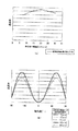
図6(a)より、帯状部22bの電極ピッチd3が10〜30[μm]の範囲内である場合に、視角制御画素Pbの透過率が高くなって、表示画面を極角度+40[°]〜+60[°]及び極角度−40[°]〜−60[°]の方向から見たときの画像のコントラストをより低くすることができる。また、その範囲内の中でも、特に、視角制御画素Pbの透過率のピークは、帯状部22bの電極ピッチd3が15〜25[μm]の間に存在している。この場合に、表示画面を極角度+40[°]〜+60[°]及び極角度−40[°]〜−60[°]の方向から見たときの画像のコントラストを最も低くすることができる。
As shown in FIG. 6A, when the electrode pitch d3 of the belt-
続いて、図6(b)に、極角度−80[°]〜+80[°]の範囲内において、帯状部22bの電極ピッチd3[μm]を適宜変化させた場合の、視角制御画素Pbの透過率(又は輝度)の視角特性のグラフの一例を示す。図6(b)において、縦軸は透過率を示し、横軸は図5(a)に対応する液晶装置1の極角度[°]を示す。なお、図6(b)において、縦軸に示す透過率は図中の上側に向かうに連れて高くなる。
Subsequently, in FIG. 6B, the viewing angle control pixel Pb when the electrode pitch d3 [μm] of the belt-
図6(b)に示すように、視角制御画素Pbの透過率のピークは、視角制御画素Pbにおける帯状部22bの電極ピッチd3の大小に拘わらず、極角度+40[°]〜+60[°]及び極角度−40[°]〜−60[°]の各範囲内に存在していることが分かる。また、図6(b)に示すグラフの例では、極角度+40[°]〜+60[°]及び極角度−40[°]〜−60[°]の各範囲内において、帯状部22bの電極ピッチd3が20[μm]、17[μm]、15[μm]、30[μm]、7[μm]の順に視角制御画素Pbの透過率のピークが大きくなり、しかも、極角度+40[°]〜+60[°]及び極角度−40[°]〜−60[°]の各範囲内においてそれらのグラフ間において視角制御画素Pbの透過率のピークの差が最も大きくなって表れている。
As shown in FIG. 6B, the transmittance peak of the viewing angle control pixel Pb is a polar angle +40 [°] to +60 [°] regardless of the size of the electrode pitch d3 of the
一方、サブ表示画素Pcの帯状部21bの電極ピッチは、帯状部21bの周期的な間隔であり、図3において、サブ表示画素Pcの略短軸方向における帯状部21bの幅d4と、サブ表示画素Pcの略短軸方向に隣り合う帯状部21b同士の間隔(=スリット21sの幅)d5との総和d6に等しい。また、サブ表示画素Pcの帯状部21bの電極ピッチd6は、高品位な表示を得る上で、通常2〜8[μm]が最適な値とされる。
On the other hand, the electrode pitch of the
以上のことから、サブ表示画素Pcと視角制御画素Pbとで最適な帯状部の電極ピッチが異なり、視角制御画素Pbの帯状部22bの電極ピッチd3を、サブ表示画素Pcの帯状部21bの電極ピッチd6より大きくすることが望ましい。これにより、狭視角表示モード時に、液晶装置1の表示画面を斜め方向から見たときの画像のコントラストをより低下させることができ、良好な狭視角表示効果を得ることができる。特に、サブ表示画素Pcの帯状部21bの電極ピッチd6を最適値である2〜8[μm]とした場合、帯状部22bの電極ピッチd3が10〜30[μm]の範囲内である場合にそのコントラストをより低くすることができ、帯状部22bの電極ピッチd3が15〜25[μm]である場合に、そのコントラストを最も低くすることができる。
From the above, the optimum electrode pitch of the belt-like portion differs between the sub display pixel Pc and the viewing angle control pixel Pb, and the electrode pitch d3 of the belt-
続いて、本実施形態では、視角制御画素Pbにおいて、帯状部22bの幅d1と、隣り合う帯状部22b同士の間隔d2との最適な関係についても検討してみた。
Subsequently, in the present embodiment, the optimum relationship between the width d1 of the belt-
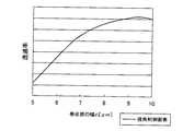
図7は、視角制御画素Pbにおいて、帯状部22bの電極ピッチd3を例えば20[μm]とした場合に、帯状部22bの幅d1を適宜変化させた場合の、帯状部22bの幅d1と透過率との関係を示すグラフである。なお、ここで、帯状部22bの電極ピッチd3を例えば20[μm]としているのは、上記したように視角制御画素Pbの透過率が最も大きくなる範囲内にあるからである。図7において、縦軸は透過率を示し、横軸は帯状部22bの幅d1[μm]を示す。なお、図7において、縦軸に示す透過率は図中の上側に向かうに連れて高くなる。
FIG. 7 shows that the width d1 of the belt-
図7より、帯状部22bの幅d1が9〜10[μm]の範囲内において視角制御画素Pbの透過率が大きくなり、帯状部22bの幅d1が約9.5[μm]のときに、視角制御画素Pbの透過率がピークとなることが分かる。ここで、帯状部22bの幅d1が9[μm]のときには、隣り合う帯状部22b同士の間隔d2は約11[μm]である。また、帯状部22bの幅d1が10[μm]のときには、隣り合う帯状部22b同士の間隔d2も約10[μm]である。また、帯状部22bの幅d1が約9.5[μm]のときには、隣り合う帯状部22b同士の間隔d2は約10.5[μm]である。
From FIG. 7, when the width d1 of the
以上のことから、良好な狭視角表示効果を得るためには、視角制御画素Pbの長軸方向に隣り合う帯状部22b同士の間隔d2が、帯状部22bの幅d1と略等しいか、又は帯状部22bの幅d1より若干大きいことが望ましい。
From the above, in order to obtain a good narrow viewing angle display effect, the interval d2 between the
[変形例]
本発明は、上記の実施形態に限定されるものではなく、本発明の趣旨を逸脱しない範囲において種々の変更を加えることが可能である。
[Modification]
The present invention is not limited to the above embodiment, and various modifications can be made without departing from the spirit of the present invention.
例えば、本発明では、誘電体層としての第2層間絶縁膜34の位置を基準とした場合に、サブ表示画素Pc及び視角制御画素Pbと共通電極39との位置関係は上下逆であっても構わない。
For example, in the present invention, when the position of the second
また、本発明では、液晶装置1の画像表示領域Vを複数の表示領域に分割して、その分割された表示領域毎に、別々の視角制御(即ち、狭視角制御と広視角制御)を行うことが可能である。
In the present invention, the image display region V of the
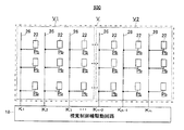
この点について、図8及び図9を参照して説明する。図8は、本発明の変形例に係る視角制御線駆動回路18とこれに電気的に接続された各視角制御線26等との電気的な構成を示す視角制御等価回路600の回路図を示す。なお、図8では、画像表示領域Vにおいて表示画素Pa等の図示は省略している。
This point will be described with reference to FIGS. FIG. 8 is a circuit diagram of a viewing angle control
この視角制御等価回路600では、{K1、K2、K3、・・・、Kn−2、Kn−1、Kn;(nは自然数)}の各視角制御用信号が供給される複数の視角制御線26が設けられている。各視角制御線26は、その延在方向に列をなす各視角制御画素Pbの画素電極22に直接的且つ電気的に接続されていると共に、視角制御線駆動回路18に電気的に接続されている。
In this visual angle control
これにより、視角制御線駆動回路18を通じて、データ線駆動回路16及び走査線駆動回路17とは独立に、各視角制御線26に対して、ON又はOFFの何れかの視角制御用信号K1、K2、K3、・・・、Kn−2、Kn−1、Knを供給することが可能となる。ここで、例えば、視角制御線駆動回路18から視角制御線26を通じて画素電極22に対して、視角制御用信号を供給(ON)することにより、狭視角表示モードを容易に実現することができる。一方、視角制御線駆動回路18から視角制御線26を通じて画素電極22に対して、視角制御用信号の供給を停止(OFF)することにより、広視角表示モードを実現することができる。
As a result, the viewing angle control signals K1 and K2 that are either ON or OFF for each viewing
したがって、この視角制御等価回路600を有する液晶装置において、例えば、いわゆる複数画面表示技術を用いて、画像表示領域Vを複数の表示領域に分割して、その分割された表示領域毎に異なる画像を表示させる場合には、その分割された表示領域毎に視角制御線駆動回路18を通じて、異なる視角制御用信号(ON信号及びOFF信号)を視角制御線26に対し同時に供給する。
Therefore, in the liquid crystal device having the viewing angle control
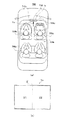
例えば、図9(a)は、この視角制御等価回路600を有する液晶装置1xを車両700のナビゲーションシステム710に適用した例を示す。図9(b)は、図9(a)の矢印Yv方向からナビゲーションシステム710を見たときの、当該ナビゲーションシステム710の表示画面710vの平面図を示す。
For example, FIG. 9A shows an example in which the
車両700の車室内700eには、運転席700aと、運転席700aに隣り合う位置に配置された助手席700bと、運転席700a及び助手席700bの後部に位置する後部座席700cと、運転席700a及び助手席700bの前方に位置するダッシュボード700dと、ダッシュボードの略中央部に設置されたナビゲーションシステム710と、を備える。ナビゲーションシステム710は、映像が映し出される表示画面710vを有する。ナビゲーションシステム710内において、その表示画面710vに対応する位置には、上記の液晶装置1xが搭載されている。ここで、運転席700aのドライバ及び助手席700bの搭乗者はナビゲーションシステム710の表示画面710vに対して斜め方向に位置していると共に、後部座席700cの搭乗者はナビゲーションシステム710の表示画面710vに対して正面方向に位置している。
A vehicle interior 700e of the
いま、このナビゲーションシステム710の表示画面710vにおいて、いわゆる2画面表示技術を用いて、その画像表示領域Vを2分割した表示領域V1、V2に対して異なる映像を表示させたとする。例えば、運転席700a側に位置する表示領域V2には行き先等を案内する地図を表示させると共に、助手席700b側に位置する表示領域V1には、地図とは異なる映像(テレビ番組、映画など)を表示させたとする。この場合、地図が表示される表示領域V2に係る各視角制御画素Pbには、対応する各視角制御線26を通じて視角制御用信号(OFF信号)を供給する一方、地図とは異なる映像が表示される表示領域V1に位置する視角制御画素Pbには、対応する各視角制御線26を通じて視角制御用信号(ON信号)を供給する。これにより、地図が表示される表示領域V2では広視角制御が行われる一方、地図とは異なる映像が表示される表示領域V1では狭視角制御が行われる。その結果、運転席200aのドライバには地図のみを見えるようにすることができ、運転上の安全性を確保できる。一方、後部座席700cの搭乗者には、地図と映像の両方を見えるようにすることができる。なお、本発明では、視角制御等価回路の構成は、図8に示すものに限定されず、本発明の趣旨を逸脱しない範囲において種々の変形をすることが可能である。
Now, it is assumed that on the
また、上記の実施形態では、第2偏光板15の吸収軸方向における斜め方向から見たときに狭視角表示効果が得られるように、画素電極21の帯状部21bの延在方向をデータ線24の延在方向に対し所定の傾斜角を以って延在する方向に規定すると共に、画素電極22の帯状部22bの延在方向をデータ線24の延在方向と略直交する方向に規定した。これに限らず、本発明では、第2偏光板15の透過軸方向(その吸収軸方向と直交する方向)における斜め方向から見たときに狭視角表示効果が得られるように、画素電極21の帯状部21bの延在方向をデータ線24の延在方向と略直交する方向に対し所定の傾斜角を以って延在する方向に規定すると共に、画素電極22の帯状部22bの延在方向をデータ線24の延在方向と略平行な方向に規定するようにしてもよい。
In the above embodiment, the extending direction of the
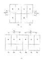
また、上記の実施形態では、表示画素Paを構成する3つのサブ表示画素Pcが一方向に配列されていると共に、視角制御画素Pbを当該一方向であって且つ表示画素Paと隣接して配列させているが、これに限らず、本発明では、それらの画素は他の配列であってもよい。例えば、図10(a)に示すように、表示画素Paを構成する3つのサブ表示画素Pcのうち、R(赤)の色光及びG(緑)の色光を出力する2つのサブ表示画素Pcを一方向に隣接して配列すると共に、B(青)の色光を出力するサブ表示画素Pcを当該一方向と略直交する方向に隣接して配列し、さらに、このB(青)の色光を出力するサブ表示画素Pcと一方向に隣接して視角制御画素Pbを配列させてもよい。 In the above embodiment, the three sub display pixels Pc constituting the display pixel Pa are arranged in one direction, and the viewing angle control pixel Pb is arranged in the one direction and adjacent to the display pixel Pa. However, the present invention is not limited to this, and in the present invention, these pixels may have other arrangements. For example, as shown in FIG. 10A, among the three sub display pixels Pc constituting the display pixel Pa, two sub display pixels Pc that output R (red) color light and G (green) color light are displayed. Sub-display pixels Pc that are arranged adjacent to one direction and that output B (blue) color light are arranged adjacent to each other in a direction substantially orthogonal to the one direction, and further, this B (blue) color light is output. The viewing angle control pixel Pb may be arranged adjacent to the sub display pixel Pc to be aligned in one direction.
また、上記の実施形態では、1つの表示画素Paに対して1つの視角制御画素Pbを配置しているが、これに限らず、本発明では、1つの表示画素Paを構成する3つのサブ表示画素Pcの各々に対応して視角制御画素Pbを配置しても良い。例えば、図10(b)に示すように、表示画素Paを構成する3つのサブ表示画素Pcの配列方向である一方向と直交する方向に3つのサブ表示画素Pcに隣接して視角制御画素Pbを配置させてもよい。このように、複数のサブ表示画素Pcの各々に対して視角制御画素Pbを配置することで、サブ表示画素Pc毎に斜め方向から見た際のコントラストを低下させることができる。したがって、視角制御画素Pbによる視角制御性能が向上する。 In the above embodiment, one viewing angle control pixel Pb is arranged for one display pixel Pa. However, the present invention is not limited to this, and in the present invention, three sub-displays constituting one display pixel Pa are provided. A viewing angle control pixel Pb may be arranged corresponding to each of the pixels Pc. For example, as shown in FIG. 10B, the viewing angle control pixel Pb is adjacent to the three sub display pixels Pc in a direction orthogonal to one direction that is the arrangement direction of the three sub display pixels Pc constituting the display pixel Pa. May be arranged. In this way, by arranging the viewing angle control pixel Pb for each of the plurality of sub display pixels Pc, it is possible to reduce the contrast when viewed from the oblique direction for each sub display pixel Pc. Therefore, the viewing angle control performance by the viewing angle control pixel Pb is improved.
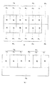
また、この構成に限らず、本発明では、複数(少なくとも1つ以上)の表示画素Paに対して1つの視角制御画素Pbを設けても良い。図11(a)は、2つの表示画素Paに対して1つの視角制御画素Pbを設けた構成例を示す。この構成例では、R、G、Bの各サブ表示画素Pcを構成する表示画素Paが田の字状に配置されている。そして、一方向に相互に隣り合う2つの表示画素Paのうち、一方の表示画素Paに対し一方向に隣接する位置には1つの視角制御画素Pbが配置されている。また、図11(b)は、2つの表示画素Paに対して1つの視角制御画素Pbを設けた他の構成例を示す。この構成例では、R、G、Bの各サブ表示画素Pcを構成する表示画素Paに対し一方向に隣接する位置には他の表示画素Paが配置されている。そして、相互に隣接する当該表示画素Pa及び当該他の表示画素Paと略直交する方向に隣接する位置には1つの視角制御画素Pbが対応して配置されている。これらの構成によれば、画像表示領域Vにおいて表示画素Paの領域を増やすことができるので、その分、表示画像の精細度を向上させることが可能となる。 Further, the present invention is not limited to this configuration. In the present invention, one viewing angle control pixel Pb may be provided for a plurality (at least one or more) of display pixels Pa. FIG. 11A shows a configuration example in which one viewing angle control pixel Pb is provided for two display pixels Pa. In this configuration example, the display pixels Pa constituting the R, G, and B sub display pixels Pc are arranged in a square shape. One viewing angle control pixel Pb is arranged at a position adjacent to one display pixel Pa in one direction among two display pixels Pa adjacent to each other in one direction. FIG. 11B shows another configuration example in which one viewing angle control pixel Pb is provided for two display pixels Pa. In this configuration example, another display pixel Pa is disposed at a position adjacent to the display pixel Pa constituting each of the R, G, and B sub-display pixels Pc in one direction. Then, one viewing angle control pixel Pb is arranged corresponding to a position adjacent to each other in the direction substantially orthogonal to the display pixel Pa and the other display pixel Pa adjacent to each other. According to these configurations, since the area of the display pixel Pa can be increased in the image display area V, the definition of the display image can be improved accordingly.
また、本発明では、サブ表示画素Pcと同様に、各視角制御画素Pbに対応するサブ表示画素Pcが表示する色と同等の色を表示するためのカラーフィルタ層を設けても良い。このとき、例えば視角制御画素Pbにおけるカラーフィルタ層の厚さをサブ表示画素Pcにおけるカラーフィルタ層の厚さより薄くしたり、或いは同等の厚さであっても視角制御画素Pbにおけるカラーフィルタ層に開口を形成したりすることなどにより、視角制御画素Pbがサブ表示画素Pcよりも強度の強い光を表示可能とすることが好ましい。これにより、視角制御画素Pbの面積をサブ表示画素Pcの面積よりも小さくしても、視角制御画素Pbとサブ表示画素Pcの各々における光の強度を揃えることができる。 In the present invention, similarly to the sub display pixel Pc, a color filter layer for displaying a color equivalent to the color displayed by the sub display pixel Pc corresponding to each viewing angle control pixel Pb may be provided. At this time, for example, the thickness of the color filter layer in the viewing angle control pixel Pb is made thinner than the thickness of the color filter layer in the sub display pixel Pc, or even if the thickness is equal, the color filter layer in the viewing angle control pixel Pb has an opening. It is preferable that the viewing angle control pixel Pb can display light having a stronger intensity than the sub display pixel Pc. Thereby, even if the area of the viewing angle control pixel Pb is made smaller than the area of the sub display pixel Pc, the light intensity in each of the viewing angle control pixel Pb and the sub display pixel Pc can be made uniform.
[電子機器]
次に、図12を参照して、本発明の実施形態に係る液晶装置1、1xを含む液晶装置の何れか(以下、代表して「液晶装置1」と称する)を用いた電子機器の一例について説明する。
[Electronics]
Next, with reference to FIG. 12, an example of an electronic apparatus using any one of the liquid crystal devices including the
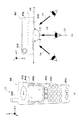
図12(a)は、本実施形態に係る液晶装置1を用いた電子機器の一例である携帯電話機800を、その表示面側から見た正面図を示す。図12(b)は、図12(a)に示す携帯電話機800を送受信アンテナ800f側(矢印Y1方向)から見たときの、当該携帯電話機800の一側面図を示す。なお、以下では、本発明の携帯電話機800の厚さ方向をZ方向と規定し、また、図12(a)に示す携帯電話機800の紙面上下方向を±Y方向と規定し、さらに、図12(a)に示す携帯電話機800の紙面左右方向を±X方向と規定する。また、極角度[°]の方向Pdrは、携帯電話機800における表示部800bの法線方向Z1に対して、その紙面左右方向に±θだけずらした角度の方向と規定する。
FIG. 12A shows a front view of a
携帯電話機800は、ケース800gの表側に設けられた、メール等の入力操作を行うための複数の操作ボタン800a、文字、図形、写真などの映像(表示画像)を表示するための表示部800b、受話口800c及び送話口800dと、各種の機能設定等を行うための機能操作ボタン800eと、ケース800gの一側面に設けられた送受信アンテナ800fと、を備えて構成される。ケース800g内であって、表示部800bに対応する位置には、本実施形態に係る液晶装置1が収容されている。このため、かかる携帯電話機800では、利用者が操作ボタン800aや機能操作ボタン800eなどを操作することにより、表示部800bに映像を表示させることが可能となっている。
The
特に、本発明の携帯電話機800は、通常の利用時にどの方向からも表示画像を観ることができる広視角表示モードと、屋外や公共の場等での利用時にメールや写真等を含む表示画像のコントラストを低下させて、利用者以外の周囲の人からその表示画像を見え難くする狭視角表示モードと、を選択的に切り替えて用いることが可能となっている。なお、この広視角表示モードと狭視角表示モードの視角切替は、利用者が操作ボタン800aや機能操作ボタン800eを操作することにより実現される。
In particular, the
この携帯電話機800において、利用者により広視角表示モードが選択された場合には、図12(b)において、表示部800bをその法線方向Z1となる正面方向Y2(Z方向)から見た場合でも、また、その法線方向Z1から表示部800bの表示面に対して+θ[°]だけ傾斜した右斜め方向Y3(+極角度方向Pdr)から表示部800bを見た場合でも、さらに、その法線方向Z1から表示部800bの表示面に対して−θ[°]だけ傾斜した左斜め方向Y4(−極角度方向Pdr)から表示部800bを見た場合でも表示画像を視認することができる。一方、利用者により狭視角表示モードが選択された場合、図12(b)において、表示部800bをその法線方向Z1から見た場合には、コントラストの高い表示画像を視認できるが、表示部800bを右斜め方向Y3(特に、極角度+40[°]以上)及び左斜め方向Y4(特に、極角度−40[°]以下)から見た場合には、液晶装置1の視角制御領域の輝度が変化して、その画像のコントラストが低下するため、表示画像を視認できなくすることができる。
In the
なお、上記の実施形態では、本発明の液晶装置1を適用可能な電子機器として携帯電話機800を一例として説明したが、これに限らず、本発明の液晶装置1を適用可能な電子機器としては、その他にも、可搬型のパーソナルコンピュータ(いわゆるノート型パソコン)、液晶テレビ、ビューファインダ型・モニタ直視型のビデオテープレコーダ、カーナビゲーション装置、ページャ、電子手帳、電卓、ワードプロセッサ、ワークステーション、テレビ電話、POS端末、ディジタルスチルカメラなどが挙げられる。
In the above embodiment, the
1、1x 液晶装置、 11 素子基板、 12 対向基板、 13 液晶層、 13a 液晶分子、 21、22 画素電極、 21b、22b 帯状部、 21s、22s スリット、 39 共通電極、 600 視角制御等価回路、 700 車両、 710 ナビゲーションシステム、 800 携帯電話機、 Pa 表示画素(表示画素領域)、 Pb 視角制御画素(視角制御画素領域)、 Pc サブ表示画素(サブ表示画素領域) 1, 1x liquid crystal device, 11 element substrate, 12 counter substrate, 13 liquid crystal layer, 13a liquid crystal molecule, 21, 22 pixel electrode, 21b, 22b strip, 21s, 22s slit, 39 common electrode, 600 viewing angle control equivalent circuit, 700 Vehicle, 710 navigation system, 800 mobile phone, Pa display pixel (display pixel area), Pb viewing angle control pixel (viewing angle control pixel area), Pc sub display pixel (sub display pixel area)
Claims (7)
前記一対の基板の平面領域内には、少なくとも1つの表示画素領域と、前記一対の基板面の正面方向において暗表示を行うと共に前記一対の基板面の法線方向に対する斜め方向において当該斜め方向に応じ輝度が変化する少なくとも1つの視角制御画素領域とを有し、
前記一対の基板のうち一方の基板において、前記表示画素領域は誘電体層を挟んで対向配置された一対の電極を有するとともに、前記視角制御画素領域も前記誘電体層を挟んで対向配置された一対の電極を有し、
前記視角制御画素領域の前記一対の電極と前記表示画素領域の前記一対の電極とはそれぞれ独立して駆動され、
前記一対の電極のうち一方の電極は、一方向に配置された複数の帯状部を有し、
前記視角制御画素領域における前記帯状部のピッチは、前記表示画素領域における前記帯状部のピッチより大きく、
前記視角制御画素領域において、前記一方向に隣り合う前記帯状部同士の間隔は、前記帯状部の幅と等しいか、又は前記帯状部の幅より大きい液晶装置。 A liquid crystal device having a liquid crystal layer sandwiched between a pair of substrates,
In the plane region of the pair of substrates, at least one display pixel region and dark display in the front direction of the pair of substrate surfaces and in the oblique direction in the oblique direction with respect to the normal direction of the pair of substrate surfaces And at least one viewing angle control pixel region whose luminance changes in response.
In one of the pair of substrates, the display pixel region has a pair of electrodes opposed to each other with a dielectric layer interposed therebetween, and the viewing angle control pixel region is also arranged to face each other with the dielectric layer interposed therebetween. Having a pair of electrodes,
The pair of electrodes in the viewing angle control pixel region and the pair of electrodes in the display pixel region are driven independently,
One of the pair of electrodes has a plurality of strips arranged in one direction,
The pitch of the strips in the viewing angle control pixel region is larger than the pitch of the strips in the display pixel region,
In the viewing angle control pixel region, the interval of the strip portions adjacent to each other in said one direction, width and equal poetry of the belt portion, or larger liquid crystal device than the width of the strip portion.
前記表示画素領域における前記帯状部のピッチは2〜8[μm]である請求項1又は2に記載の液晶装置。 The pitch of the strips in the viewing angle control pixel region is 10 to 30 [μm],
The pitch of the belt portion in the display pixel area liquid crystal device according to 請 Motomeko 1 or 2 Ru der 2~8 [μm].
Priority Applications (1)
| Application Number | Priority Date | Filing Date | Title |
|---|---|---|---|
| JP2008076118A JP5477884B2 (en) | 2008-03-24 | 2008-03-24 | Liquid crystal device and electronic device |
Applications Claiming Priority (1)
| Application Number | Priority Date | Filing Date | Title |
|---|---|---|---|
| JP2008076118A JP5477884B2 (en) | 2008-03-24 | 2008-03-24 | Liquid crystal device and electronic device |
Publications (2)
| Publication Number | Publication Date |
|---|---|
| JP2009229891A JP2009229891A (en) | 2009-10-08 |
| JP5477884B2 true JP5477884B2 (en) | 2014-04-23 |
Family
ID=41245344
Family Applications (1)
| Application Number | Title | Priority Date | Filing Date |
|---|---|---|---|
| JP2008076118A Expired - Fee Related JP5477884B2 (en) | 2008-03-24 | 2008-03-24 | Liquid crystal device and electronic device |
Country Status (1)
| Country | Link |
|---|---|
| JP (1) | JP5477884B2 (en) |
Cited By (1)
| Publication number | Priority date | Publication date | Assignee | Title |
|---|---|---|---|---|
| CN104597676A (en) * | 2015-02-13 | 2015-05-06 | 厦门天马微电子有限公司 | Liquid crystal display panel and manufacturing method thereof |
Families Citing this family (3)
| Publication number | Priority date | Publication date | Assignee | Title |
|---|---|---|---|---|
| CN103645590B (en) * | 2013-12-12 | 2016-10-05 | 京东方科技集团股份有限公司 | A kind of array base palte and preparation method thereof, liquid crystal indicator |
| CN105093723A (en) * | 2015-09-08 | 2015-11-25 | 深圳市华星光电技术有限公司 | Liquid crystal display panel capable of improving color error |
| KR101894336B1 (en) * | 2015-12-24 | 2018-09-03 | 엘지디스플레이 주식회사 | Liquid crystal display panel and liquid crystal display having the same |
Family Cites Families (3)
| Publication number | Priority date | Publication date | Assignee | Title |
|---|---|---|---|---|
| GB9811477D0 (en) * | 1998-05-29 | 1998-07-29 | Sharp Kk | Liquid crystal device |
| JP4813842B2 (en) * | 2005-07-29 | 2011-11-09 | 株式会社 日立ディスプレイズ | Liquid crystal display |
| JP5113333B2 (en) * | 2005-12-28 | 2013-01-09 | エルジー ディスプレイ カンパニー リミテッド | Liquid crystal display |
-
2008
- 2008-03-24 JP JP2008076118A patent/JP5477884B2/en not_active Expired - Fee Related
Cited By (3)
| Publication number | Priority date | Publication date | Assignee | Title |
|---|---|---|---|---|
| CN104597676A (en) * | 2015-02-13 | 2015-05-06 | 厦门天马微电子有限公司 | Liquid crystal display panel and manufacturing method thereof |
| CN104597676B (en) * | 2015-02-13 | 2018-06-26 | 厦门天马微电子有限公司 | A kind of liquid crystal display panel and its manufacturing method |
| US10114248B2 (en) | 2015-02-13 | 2018-10-30 | Xiamen Tianma Micro-Electronics Co., Ltd. | Liquid crystal display panel and fabrication method thereof |
Also Published As
| Publication number | Publication date |
|---|---|
| JP2009229891A (en) | 2009-10-08 |
Similar Documents
| Publication | Publication Date | Title |
|---|---|---|
| JP2009229800A (en) | Liquid crystal display device and electronic equipment | |
| CN100578326C (en) | Liquid crystal device and electronic equipment | |
| US7990506B2 (en) | Liquid crystal display device and electronic apparatus | |
| JP5489267B2 (en) | Liquid crystal devices and electronic devices | |
| US10088714B2 (en) | Liquid crystal display device | |
| JP4607158B2 (en) | Liquid crystal display device and electronic device | |
| CN101446715A (en) | Liquid crystal apparatus and electronic device | |
| JP2007226175A (en) | Liquid crystal device and electronic equipment | |
| JP4569836B2 (en) | Liquid crystal device | |
| EP2765493A2 (en) | Display panel capable of detecting touch and display apparatus having the same | |
| US20180314098A1 (en) | Display board and display device | |
| JP5110991B2 (en) | Liquid crystal device and electronic device | |
| JP5106991B2 (en) | Liquid crystal device and electronic device | |
| JP5477884B2 (en) | Liquid crystal device and electronic device | |
| JP5175133B2 (en) | Liquid crystal device and electronic device | |
| CN115390317B (en) | Display device | |
| US10718982B2 (en) | Liquid crystal display devices | |
| JP2009229890A (en) | Liquid crystal device and electronic equipment | |
| JP2009020315A (en) | Liquid crystal device and electronic apparatus | |
| JP2009223099A (en) | Liquid crystal display device and electronic apparatus | |
| JP2007226200A (en) | Liquid crystal device, and electronic device | |
| JP4940954B2 (en) | Liquid crystal device and electronic device | |
| JP5017677B2 (en) | Liquid crystal display | |
| JP2008083324A (en) | Liquid crystal display device and electronic device | |
| US8742416B2 (en) | Display panel, method of manufacturing display panel, display device, and electronic apparatus |
Legal Events
| Date | Code | Title | Description |
|---|---|---|---|
| A711 | Notification of change in applicant |
Free format text: JAPANESE INTERMEDIATE CODE: A711 Effective date: 20100526 |
|
| RD02 | Notification of acceptance of power of attorney |
Free format text: JAPANESE INTERMEDIATE CODE: A7422 Effective date: 20100526 |
|
| A621 | Written request for application examination |
Free format text: JAPANESE INTERMEDIATE CODE: A621 Effective date: 20110112 |
|
| A711 | Notification of change in applicant |
Free format text: JAPANESE INTERMEDIATE CODE: A711 Effective date: 20120330 |
|
| A131 | Notification of reasons for refusal |
Free format text: JAPANESE INTERMEDIATE CODE: A131 Effective date: 20120703 |
|
| A977 | Report on retrieval |
Free format text: JAPANESE INTERMEDIATE CODE: A971007 Effective date: 20120704 |
|
| A521 | Written amendment |
Free format text: JAPANESE INTERMEDIATE CODE: A523 Effective date: 20120823 |
|
| A131 | Notification of reasons for refusal |
Free format text: JAPANESE INTERMEDIATE CODE: A131 Effective date: 20130423 |
|
| TRDD | Decision of grant or rejection written | ||
| A01 | Written decision to grant a patent or to grant a registration (utility model) |
Free format text: JAPANESE INTERMEDIATE CODE: A01 Effective date: 20140121 |
|
| A711 | Notification of change in applicant |
Free format text: JAPANESE INTERMEDIATE CODE: A712 Effective date: 20140206 |
|
| A61 | First payment of annual fees (during grant procedure) |
Free format text: JAPANESE INTERMEDIATE CODE: A61 Effective date: 20140206 |
|
| R150 | Certificate of patent or registration of utility model |
Ref document number: 5477884 Country of ref document: JP Free format text: JAPANESE INTERMEDIATE CODE: R150 |
|
| LAPS | Cancellation because of no payment of annual fees |